EP2381464B1 - Vorrichtung und Verfahren zum Ablösen eines Produktsubstrats von einem Trägersubstrat - Google Patents
Vorrichtung und Verfahren zum Ablösen eines Produktsubstrats von einem Trägersubstrat Download PDFInfo
- Publication number
- EP2381464B1 EP2381464B1 EP10004313A EP10004313A EP2381464B1 EP 2381464 B1 EP2381464 B1 EP 2381464B1 EP 10004313 A EP10004313 A EP 10004313A EP 10004313 A EP10004313 A EP 10004313A EP 2381464 B1 EP2381464 B1 EP 2381464B1
- Authority
- EP
- European Patent Office
- Prior art keywords
- solvent
- product substrate
- film
- substrate
- bonding layer
- Prior art date
- Legal status (The legal status is an assumption and is not a legal conclusion. Google has not performed a legal analysis and makes no representation as to the accuracy of the status listed.)
- Active
Links
Images
Classifications
-
- H—ELECTRICITY
- H01—ELECTRIC ELEMENTS
- H01L—SEMICONDUCTOR DEVICES NOT COVERED BY CLASS H10
- H01L21/00—Processes or apparatus adapted for the manufacture or treatment of semiconductor or solid state devices or of parts thereof
- H01L21/67—Apparatus specially adapted for handling semiconductor or electric solid state devices during manufacture or treatment thereof; Apparatus specially adapted for handling wafers during manufacture or treatment of semiconductor or electric solid state devices or components ; Apparatus not specifically provided for elsewhere
- H01L21/67005—Apparatus not specifically provided for elsewhere
- H01L21/67011—Apparatus for manufacture or treatment
- H01L21/67092—Apparatus for mechanical treatment
-
- B—PERFORMING OPERATIONS; TRANSPORTING
- B32—LAYERED PRODUCTS
- B32B—LAYERED PRODUCTS, i.e. PRODUCTS BUILT-UP OF STRATA OF FLAT OR NON-FLAT, e.g. CELLULAR OR HONEYCOMB, FORM
- B32B38/00—Ancillary operations in connection with laminating processes
- B32B38/10—Removing layers, or parts of layers, mechanically or chemically
-
- H—ELECTRICITY
- H01—ELECTRIC ELEMENTS
- H01L—SEMICONDUCTOR DEVICES NOT COVERED BY CLASS H10
- H01L21/00—Processes or apparatus adapted for the manufacture or treatment of semiconductor or solid state devices or of parts thereof
- H01L21/02—Manufacture or treatment of semiconductor devices or of parts thereof
-
- B—PERFORMING OPERATIONS; TRANSPORTING
- B32—LAYERED PRODUCTS
- B32B—LAYERED PRODUCTS, i.e. PRODUCTS BUILT-UP OF STRATA OF FLAT OR NON-FLAT, e.g. CELLULAR OR HONEYCOMB, FORM
- B32B37/00—Methods or apparatus for laminating, e.g. by curing or by ultrasonic bonding
- B32B37/02—Methods or apparatus for laminating, e.g. by curing or by ultrasonic bonding characterised by a sequence of laminating steps, e.g. by adding new layers at consecutive laminating stations
- B32B37/025—Transfer laminating
-
- H—ELECTRICITY
- H01—ELECTRIC ELEMENTS
- H01L—SEMICONDUCTOR DEVICES NOT COVERED BY CLASS H10
- H01L21/00—Processes or apparatus adapted for the manufacture or treatment of semiconductor or solid state devices or of parts thereof
- H01L21/67—Apparatus specially adapted for handling semiconductor or electric solid state devices during manufacture or treatment thereof; Apparatus specially adapted for handling wafers during manufacture or treatment of semiconductor or electric solid state devices or components ; Apparatus not specifically provided for elsewhere
- H01L21/67005—Apparatus not specifically provided for elsewhere
- H01L21/67011—Apparatus for manufacture or treatment
- H01L21/67132—Apparatus for placing on an insulating substrate, e.g. tape
-
- H—ELECTRICITY
- H01—ELECTRIC ELEMENTS
- H01L—SEMICONDUCTOR DEVICES NOT COVERED BY CLASS H10
- H01L21/00—Processes or apparatus adapted for the manufacture or treatment of semiconductor or solid state devices or of parts thereof
- H01L21/67—Apparatus specially adapted for handling semiconductor or electric solid state devices during manufacture or treatment thereof; Apparatus specially adapted for handling wafers during manufacture or treatment of semiconductor or electric solid state devices or components ; Apparatus not specifically provided for elsewhere
- H01L21/67005—Apparatus not specifically provided for elsewhere
- H01L21/67011—Apparatus for manufacture or treatment
- H01L21/6715—Apparatus for applying a liquid, a resin, an ink or the like
-
- H—ELECTRICITY
- H01—ELECTRIC ELEMENTS
- H01L—SEMICONDUCTOR DEVICES NOT COVERED BY CLASS H10
- H01L21/00—Processes or apparatus adapted for the manufacture or treatment of semiconductor or solid state devices or of parts thereof
- H01L21/67—Apparatus specially adapted for handling semiconductor or electric solid state devices during manufacture or treatment thereof; Apparatus specially adapted for handling wafers during manufacture or treatment of semiconductor or electric solid state devices or components ; Apparatus not specifically provided for elsewhere
- H01L21/677—Apparatus specially adapted for handling semiconductor or electric solid state devices during manufacture or treatment thereof; Apparatus specially adapted for handling wafers during manufacture or treatment of semiconductor or electric solid state devices or components ; Apparatus not specifically provided for elsewhere for conveying, e.g. between different workstations
-
- B—PERFORMING OPERATIONS; TRANSPORTING
- B32—LAYERED PRODUCTS
- B32B—LAYERED PRODUCTS, i.e. PRODUCTS BUILT-UP OF STRATA OF FLAT OR NON-FLAT, e.g. CELLULAR OR HONEYCOMB, FORM
- B32B38/00—Ancillary operations in connection with laminating processes
- B32B2038/0052—Other operations not otherwise provided for
-
- B—PERFORMING OPERATIONS; TRANSPORTING
- B32—LAYERED PRODUCTS
- B32B—LAYERED PRODUCTS, i.e. PRODUCTS BUILT-UP OF STRATA OF FLAT OR NON-FLAT, e.g. CELLULAR OR HONEYCOMB, FORM
- B32B2307/00—Properties of the layers or laminate
- B32B2307/50—Properties of the layers or laminate having particular mechanical properties
- B32B2307/546—Flexural strength; Flexion stiffness
-
- B—PERFORMING OPERATIONS; TRANSPORTING
- B32—LAYERED PRODUCTS
- B32B—LAYERED PRODUCTS, i.e. PRODUCTS BUILT-UP OF STRATA OF FLAT OR NON-FLAT, e.g. CELLULAR OR HONEYCOMB, FORM
- B32B2310/00—Treatment by energy or chemical effects
- B32B2310/04—Treatment by energy or chemical effects using liquids, gas or steam
- B32B2310/0409—Treatment by energy or chemical effects using liquids, gas or steam using liquids
- B32B2310/0418—Treatment by energy or chemical effects using liquids, gas or steam using liquids other than water
-
- B—PERFORMING OPERATIONS; TRANSPORTING
- B32—LAYERED PRODUCTS
- B32B—LAYERED PRODUCTS, i.e. PRODUCTS BUILT-UP OF STRATA OF FLAT OR NON-FLAT, e.g. CELLULAR OR HONEYCOMB, FORM
- B32B43/00—Operations specially adapted for layered products and not otherwise provided for, e.g. repairing; Apparatus therefor
- B32B43/006—Delaminating
-
- H—ELECTRICITY
- H01—ELECTRIC ELEMENTS
- H01L—SEMICONDUCTOR DEVICES NOT COVERED BY CLASS H10
- H01L21/00—Processes or apparatus adapted for the manufacture or treatment of semiconductor or solid state devices or of parts thereof
- H01L21/67—Apparatus specially adapted for handling semiconductor or electric solid state devices during manufacture or treatment thereof; Apparatus specially adapted for handling wafers during manufacture or treatment of semiconductor or electric solid state devices or components ; Apparatus not specifically provided for elsewhere
- H01L21/673—Apparatus specially adapted for handling semiconductor or electric solid state devices during manufacture or treatment thereof; Apparatus specially adapted for handling wafers during manufacture or treatment of semiconductor or electric solid state devices or components ; Apparatus not specifically provided for elsewhere using specially adapted carriers or holders; Fixing the workpieces on such carriers or holders
- H01L21/67346—Apparatus specially adapted for handling semiconductor or electric solid state devices during manufacture or treatment thereof; Apparatus specially adapted for handling wafers during manufacture or treatment of semiconductor or electric solid state devices or components ; Apparatus not specifically provided for elsewhere using specially adapted carriers or holders; Fixing the workpieces on such carriers or holders characterized by being specially adapted for supporting a single substrate or by comprising a stack of such individual supports
-
- H—ELECTRICITY
- H01—ELECTRIC ELEMENTS
- H01L—SEMICONDUCTOR DEVICES NOT COVERED BY CLASS H10
- H01L21/00—Processes or apparatus adapted for the manufacture or treatment of semiconductor or solid state devices or of parts thereof
- H01L21/67—Apparatus specially adapted for handling semiconductor or electric solid state devices during manufacture or treatment thereof; Apparatus specially adapted for handling wafers during manufacture or treatment of semiconductor or electric solid state devices or components ; Apparatus not specifically provided for elsewhere
- H01L21/683—Apparatus specially adapted for handling semiconductor or electric solid state devices during manufacture or treatment thereof; Apparatus specially adapted for handling wafers during manufacture or treatment of semiconductor or electric solid state devices or components ; Apparatus not specifically provided for elsewhere for supporting or gripping
- H01L21/687—Apparatus specially adapted for handling semiconductor or electric solid state devices during manufacture or treatment thereof; Apparatus specially adapted for handling wafers during manufacture or treatment of semiconductor or electric solid state devices or components ; Apparatus not specifically provided for elsewhere for supporting or gripping using mechanical means, e.g. chucks, clamps or pinches
- H01L21/68714—Apparatus specially adapted for handling semiconductor or electric solid state devices during manufacture or treatment thereof; Apparatus specially adapted for handling wafers during manufacture or treatment of semiconductor or electric solid state devices or components ; Apparatus not specifically provided for elsewhere for supporting or gripping using mechanical means, e.g. chucks, clamps or pinches the wafers being placed on a susceptor, stage or support
- H01L21/68721—Apparatus specially adapted for handling semiconductor or electric solid state devices during manufacture or treatment thereof; Apparatus specially adapted for handling wafers during manufacture or treatment of semiconductor or electric solid state devices or components ; Apparatus not specifically provided for elsewhere for supporting or gripping using mechanical means, e.g. chucks, clamps or pinches the wafers being placed on a susceptor, stage or support characterised by edge clamping, e.g. clamping ring
-
- H—ELECTRICITY
- H01—ELECTRIC ELEMENTS
- H01L—SEMICONDUCTOR DEVICES NOT COVERED BY CLASS H10
- H01L21/00—Processes or apparatus adapted for the manufacture or treatment of semiconductor or solid state devices or of parts thereof
- H01L21/67—Apparatus specially adapted for handling semiconductor or electric solid state devices during manufacture or treatment thereof; Apparatus specially adapted for handling wafers during manufacture or treatment of semiconductor or electric solid state devices or components ; Apparatus not specifically provided for elsewhere
- H01L21/683—Apparatus specially adapted for handling semiconductor or electric solid state devices during manufacture or treatment thereof; Apparatus specially adapted for handling wafers during manufacture or treatment of semiconductor or electric solid state devices or components ; Apparatus not specifically provided for elsewhere for supporting or gripping
- H01L21/687—Apparatus specially adapted for handling semiconductor or electric solid state devices during manufacture or treatment thereof; Apparatus specially adapted for handling wafers during manufacture or treatment of semiconductor or electric solid state devices or components ; Apparatus not specifically provided for elsewhere for supporting or gripping using mechanical means, e.g. chucks, clamps or pinches
- H01L21/68714—Apparatus specially adapted for handling semiconductor or electric solid state devices during manufacture or treatment thereof; Apparatus specially adapted for handling wafers during manufacture or treatment of semiconductor or electric solid state devices or components ; Apparatus not specifically provided for elsewhere for supporting or gripping using mechanical means, e.g. chucks, clamps or pinches the wafers being placed on a susceptor, stage or support
- H01L21/68771—Apparatus specially adapted for handling semiconductor or electric solid state devices during manufacture or treatment thereof; Apparatus specially adapted for handling wafers during manufacture or treatment of semiconductor or electric solid state devices or components ; Apparatus not specifically provided for elsewhere for supporting or gripping using mechanical means, e.g. chucks, clamps or pinches the wafers being placed on a susceptor, stage or support characterised by supporting more than one semiconductor substrate
-
- H—ELECTRICITY
- H01—ELECTRIC ELEMENTS
- H01L—SEMICONDUCTOR DEVICES NOT COVERED BY CLASS H10
- H01L2221/00—Processes or apparatus adapted for the manufacture or treatment of semiconductor or solid state devices or of parts thereof covered by H01L21/00
- H01L2221/67—Apparatus for handling semiconductor or electric solid state devices during manufacture or treatment thereof; Apparatus for handling wafers during manufacture or treatment of semiconductor or electric solid state devices or components; Apparatus not specifically provided for elsewhere
- H01L2221/683—Apparatus for handling semiconductor or electric solid state devices during manufacture or treatment thereof; Apparatus for handling wafers during manufacture or treatment of semiconductor or electric solid state devices or components; Apparatus not specifically provided for elsewhere for supporting or gripping
- H01L2221/68304—Apparatus for handling semiconductor or electric solid state devices during manufacture or treatment thereof; Apparatus for handling wafers during manufacture or treatment of semiconductor or electric solid state devices or components; Apparatus not specifically provided for elsewhere for supporting or gripping using temporarily an auxiliary support
- H01L2221/68381—Details of chemical or physical process used for separating the auxiliary support from a device or wafer
- H01L2221/68386—Separation by peeling
-
- Y—GENERAL TAGGING OF NEW TECHNOLOGICAL DEVELOPMENTS; GENERAL TAGGING OF CROSS-SECTIONAL TECHNOLOGIES SPANNING OVER SEVERAL SECTIONS OF THE IPC; TECHNICAL SUBJECTS COVERED BY FORMER USPC CROSS-REFERENCE ART COLLECTIONS [XRACs] AND DIGESTS
- Y10—TECHNICAL SUBJECTS COVERED BY FORMER USPC
- Y10T—TECHNICAL SUBJECTS COVERED BY FORMER US CLASSIFICATION
- Y10T156/00—Adhesive bonding and miscellaneous chemical manufacture
- Y10T156/11—Methods of delaminating, per se; i.e., separating at bonding face
- Y10T156/1111—Using solvent during delaminating [e.g., water dissolving adhesive at bonding face during delamination, etc.]
-
- Y—GENERAL TAGGING OF NEW TECHNOLOGICAL DEVELOPMENTS; GENERAL TAGGING OF CROSS-SECTIONAL TECHNOLOGIES SPANNING OVER SEVERAL SECTIONS OF THE IPC; TECHNICAL SUBJECTS COVERED BY FORMER USPC CROSS-REFERENCE ART COLLECTIONS [XRACs] AND DIGESTS
- Y10—TECHNICAL SUBJECTS COVERED BY FORMER USPC
- Y10T—TECHNICAL SUBJECTS COVERED BY FORMER US CLASSIFICATION
- Y10T156/00—Adhesive bonding and miscellaneous chemical manufacture
- Y10T156/11—Methods of delaminating, per se; i.e., separating at bonding face
- Y10T156/1168—Gripping and pulling work apart during delaminating
- Y10T156/1179—Gripping and pulling work apart during delaminating with poking during delaminating [e.g., jabbing, etc.]
-
- Y—GENERAL TAGGING OF NEW TECHNOLOGICAL DEVELOPMENTS; GENERAL TAGGING OF CROSS-SECTIONAL TECHNOLOGIES SPANNING OVER SEVERAL SECTIONS OF THE IPC; TECHNICAL SUBJECTS COVERED BY FORMER USPC CROSS-REFERENCE ART COLLECTIONS [XRACs] AND DIGESTS
- Y10—TECHNICAL SUBJECTS COVERED BY FORMER USPC
- Y10T—TECHNICAL SUBJECTS COVERED BY FORMER US CLASSIFICATION
- Y10T156/00—Adhesive bonding and miscellaneous chemical manufacture
- Y10T156/19—Delaminating means
- Y10T156/1922—Vibrating delaminating means
-
- Y—GENERAL TAGGING OF NEW TECHNOLOGICAL DEVELOPMENTS; GENERAL TAGGING OF CROSS-SECTIONAL TECHNOLOGIES SPANNING OVER SEVERAL SECTIONS OF THE IPC; TECHNICAL SUBJECTS COVERED BY FORMER USPC CROSS-REFERENCE ART COLLECTIONS [XRACs] AND DIGESTS
- Y10—TECHNICAL SUBJECTS COVERED BY FORMER USPC
- Y10T—TECHNICAL SUBJECTS COVERED BY FORMER US CLASSIFICATION
- Y10T156/00—Adhesive bonding and miscellaneous chemical manufacture
- Y10T156/19—Delaminating means
- Y10T156/1928—Differential fluid pressure delaminating means
-
- Y—GENERAL TAGGING OF NEW TECHNOLOGICAL DEVELOPMENTS; GENERAL TAGGING OF CROSS-SECTIONAL TECHNOLOGIES SPANNING OVER SEVERAL SECTIONS OF THE IPC; TECHNICAL SUBJECTS COVERED BY FORMER USPC CROSS-REFERENCE ART COLLECTIONS [XRACs] AND DIGESTS
- Y10—TECHNICAL SUBJECTS COVERED BY FORMER USPC
- Y10T—TECHNICAL SUBJECTS COVERED BY FORMER US CLASSIFICATION
- Y10T156/00—Adhesive bonding and miscellaneous chemical manufacture
- Y10T156/19—Delaminating means
- Y10T156/1978—Delaminating bending means
- Y10T156/1983—Poking delaminating means
Definitions
- the invention relates to a device according to claim 1 and a method according to claim 10 for detaching a product substrate from a carrier substrate.
- the thinning of product substrates is often required in the semiconductor industry and can be mechanical and / or chemical.
- the product substrates are usually temporarily fixed to a carrier, with different methods of fixation.
- the carrier material used is, for example, films, glass substrates or silicon wafers.
- the publication US 2009/305617 A1 shows a carrier device for receiving wafers with a supply chamber for solvent to reduce the bond strength.
- Other devices are in the US 2007/295458 A1 and the DE 197 34 635 A1 shown.
- the detachment is increasingly considered to be one of the most critical process steps, since the thin substrates with substrate thicknesses of a few microns easily break during peeling / peeling or suffer from the necessary forces for the process of detachment forces.
- the thin substrates have little to no dimensional stability and typically curl without support material.
- fixing and supporting the wafers is practically unavoidable.
- the invention is based on the idea of a generic device or a generic method thereby by introducing solvent into a solvent container formed by the film frame and the film attached thereto.
- the elasticity or flexibility of the film mounted on the film frame also makes it possible to make the solvent container variable in volume, and the elasticity or flexibility of the film is also used to gently strip the product substrate from the edge of the product substrate. In this way, the product substrate is immediately after separation available for further process steps and is protected by the film and the film frame. Many process steps can be performed directly on the film frame mounted product substrate.
- product substrate is meant a product substrate, for example a semiconductor wafer, which is usually thinned to a thickness of between 0.5 ⁇ m and 250 ⁇ m, with the tendency for ever thinner product substrates.
- the present invention operates with product substrates that themselves have similar flexibility to the film frame mounted film.
- the product substrate is peeled off the carrier substrate in the device according to the invention or the method according to the invention, in particular starting concentrically from the circumference of the product substrate.
- the carrier used is, for example, a carrier substrate having a thickness of between 50 ⁇ m and 5,000 ⁇ m, in particular between 500 ⁇ m and 1000 ⁇ m.
- the bonding layer is an adhesive, for example, a releasable adhesive, in particular a thermoplastic in question, for example, selectively in an edge region of the carrier-product substrate composite, Alternatively, the adhesive can be applied over the entire surface, whereby the adhesive force in the center can be reduced by an adhesion-reducing layer, for example a fluoropolymer, preferably Teflon.
- an adhesion-reducing layer for example a fluoropolymer, preferably Teflon.
- a receiving device is a chuck, in particular a spinner chuck for receiving the carrier substrate, in particular by means of negative pressure, for example on suction tracks, bores or suction cups.
- a mechanical recording for example by lateral brackets, conceivable.
- the recording takes place electrostatically.
- the release means comprises the film mounted on the film frame and a film frame receiving and force loading film frame receiver.
- the solvent is designed to operate substantially free of heating.
- the solvent is preferably used at ambient temperature. In this way it is possible to dispense with any heating device.
- connection layers comprising different adhesives make it possible to dissolve a specific connecting layer selectively or in defined regions.
- the chemical dissolution of the bonding view is particularly gentle for the product substrate and with a suitable choice of material, the dissolution can also be very fast, especially if only edge regions of the product substrate are provided with a bonding layer, so that the solvent can act quickly from the side. In this way it is possible to dispense with perforations in the carrier substrate and / or product substrate.
- the solvent container is formed such that the solvent acts at least at the beginning of the release of the bonding layer, in particular exclusively, in the region of a circumference of the product substrate, may be on an action of the product substrate and / or carrier substrate from the top and / or bottom, in particular one Within the side edge lying inside area of the product substrate can be dispensed with.
- the detachment means are designed to effect a force F s acting on the carrier substrate and a force F f directed against the force F s and acting on the film frame.
- the force F f acts on the circumference of the film frame, in particular at least two circumferentially distributed locations of the film frame, wherein the forces F f1 and F f2 in one Advantageous embodiment can be controlled differently to replace the product substrate from the side with the larger force F f .
- the film in particular by the force Fs and the force Ff, can be tensioned in a detachment section lying between the contacting surface section and the fastening section.
- the detachment is effected gently on the circumference of the product substrate. The release by the solvent and the detachment by the forces F s and F f supports each other.
- a vibration generator acting on the solvent and / or the bonding layer, in particular on the film and / or insertable into the solvent in the solvent container is provided.
- Applicable includes both surface contact and at least partial immersion. This supports the dissolution by the solvent and accelerates the dissolution process by at least a factor of 2, with optimized design by a factor of 5, more preferably by a factor of 10 to 50.
- the Schwringungserzeuger acts by ultrasonic waves, in particular in the region of the Kunststofftechnischabêts.
- the solvent container is trough-shaped, whereby the detachment of the product substrate can be achieved with a minimum solvent consumption.
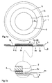
- FIG. 1a is a film frame 1 in this embodiment, at least on an inner circumference li circular film shown on its underside in accordance with the in FIG. 1b shown sectional view of a film 3 with its adhesive layer 3s is glued concentrically to the film frame 1.
- a product substrate-carrier substrate composite is adhered to the adhesive layer 3s of the film 3 concentrically with the film frame 1.
- the product substrate-carrier substrate composite consists of a product substrate 4 adhered to the film 3, a carrier substrate 2 and a bonding layer 6 connecting the product substrate 4 and the carrier substrate 2.
- the diameters of the product substrate 4 and the carrier substrate 2 are substantially identical, while the thickness of the product substrate 4 Product substrate 4 is less than the thickness of the carrier substrate. 2
- the film 3 consists of a ring-shaped fastening section 3b in the present case, in which the film 3 is fixed to the film frame 1. Furthermore, the film 3 consists of an IContakt michs SQLabrough 3k, in which the product substrate 4 is fixable to the adhesive layer 3s of the film 3. Between the attachment portion 3b and the contacting surface portion 3k is a detachment portion 3a arranged, in particular concentric with the attachment portion 3b and the contacting surface portion 3k, which does not have to have an adhesive function, but which has a decisive function according to the invention.
- the detachment portion 3a thus extends from a periphery 4u of the product substrate 4 to the inner periphery 1i of the film frame 1, in the present case as a radial distance A. designated.
- the ratio between a thickness D of the film frame 1 and the distance A is advantageously at least 1: 2 to 1:50, in particular 1: 5 to 1:25.
- FIG. 1b As shown starting position, the film 3 contacting side of the product substrate 4 and the film 3 contacting side of the film frame 1 are arranged in alignment and in a plane E.
- the in the FIGS. 1a and 1b parts shown are assembled on a known film frame mounter.
- the film 3 and the inner periphery 1 of the film frame 1 form a trough-shaped solvent container 20 in which the product substrate-carrier substrate composite can be arranged as described above.
- solvent shown 22 by introduction means 23 in the solvent container 20 can be introduced.
- the introduction means 23 in the present case consist of a line 24 and a solvent reservoir 25 which can be controlled by a central unit in order to introduce solvent 22 into the solvent container 20.
- the solvent container 20 is variable in volume by the elastic film 3, which is elastic at least in the detachment section 3a, in that a force F s acts on the carrier substrate 2 downward and a force F f acts on the film frame 1.
- the introduction of force is also controlled by a central unit.
- Enlarging the storage container volume prevents solvent 22 from running over the edge of the film frame 1 and at the same time a rapid distribution or introduction of the solvent 22 is made possible.
- the force F s is according to FIG. 3 transmitted via a carrier substrate receptacle 7 for receiving the carrier substrate 2, wherein the fixing of the carrier substrate 2 takes place on the carrier substrate receptacle 7 by incorporated into the surface of the carrier substrate receptacle 7 vacuum webs 8 and connected thereto, not dargschreib vacuum device.
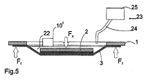
- an acoustic wave generator 10 in particular for generating ultrasonic waves, can be arranged, by which ultrasonic waves can be transmitted to the product substrate 4, but in particular to the bonding layer 6 and the solvent 22, as a result of the process of L Kunststoffs is greatly accelerated, in particular by a factor of 2, preferably by a factor of 5, more preferably by a factor of 10 to 50.
- the sound wave generator 10 is in contact at least with the surface of the fluid solvent 22, but is preferably at least partially immersed therein.
- the sound waves can be transmitted directly to the solvent 22 and from the solvent 22 to the bonding layer 6.
- the force F f acting on the film frame 1 can - as in FIG. 3 shown - evenly distributed as a surface force acting on the film frame 1, so that on the deformation of the film 3 in the detachment section 3a the volume change of the solvent container 20 can be effected.
- the force F f1 or a plurality of forces F f1 , F f2 to F fn can / may be introduced at points distributed on the circumference of the film frame 1 or distributed by a film frame recording introduced.
- the receiving device for introducing the force into the film frame 1 a tilting of the film frame 1 must be permitting.
- FIG. 3 illustrated method step of dissolution by the solvent 22 and in FIG. 4 illustrated step of detachment by opposing forces F s , F f1 , F f2 , F fn may be provided a method step by which the solvent 22 is removed from the solvent container 20, in particular by suction.
Description
- Die Erfindung betrifft eine Vorrichtung gemäß Anspruch 1 und ein Verfahren gemäß Anspruch 10 zum Ablösen eines Produktsubstrats von einem Trägersubstrat.
- Das Rückdünnen von Produktsubstraten ist in der Halbleiterindustrie häufig erforderlich und kann mechanisch und/oder chemisch erfolgen. Zum Rückdünnen werden die Produktsubstrat in der Regel auf einen Träger vorübergehend fixiert, wobei es für die Fixierung verschiedene Methoden gibt. Als Trägermaterial werden beispielsweise Folien, Glassubstrate oder Siliziumwafer verwendet.
- Die Druckschrift
US 2009/305617 A1 zeigt eine Trägervorrichtung zur Aufnahme von Wafern mit einer Zuführkammer für Lösungsmittel zur Reduzierung der Bondstärke. Weitere Vorrichtungen sind in derUS 2007/295458 A1 und derDE 197 34 635 A1 gezeigt. - In Abhängigkeit von den verwendeten Trägermaterialien und der verwendeten Verbindungsschicht zwischen Träger und Produktsubstrat sind verschiedene Verfahren zur Auflösung oder Zerstörung der Verbindungsschicht bekannt, wie beispielsweise die Verwendung von UV-Licht, Laserstrahlen, Temperatureinwirkung oder Lösungsmittel.
- Das Ablösen stellt sich zunehmend als einer der kritischsten Prozessschritte dar, da die dünnen Substrate mit Substratdicken von wenigen µm beim Ablösen/Abziehen leicht brechen oder durch die für den Vorgang des Ablösens notwendigen Kräfte Schaden erleiden.
- Darüber hinaus haben die dünnen Substrate kaum bis keine Formstabilität und rollen sich typischerweise ohne Stützmaterial ein. Während der Handhabung der rückgedünnten Wafer ist mithin eine Fixierung und Unterstützung der Wafer praktisch unumgänglich.
- Es ist daher die Aufgabe der vorliegenden Erfindung, eine Vorrichtung und ein Verfahren anzugeben, um einen Produktsubstrat möglichst zerstörungsfrei und einfach von einem Träger zu lösen.
- Diese Aufgabe wird mit den Merkmalen der Ansprüche 1 und 10 gelöst. Vorteilhafte Weiterbildungen der Erfindung sind in den Unteransprüchen angegeben. In den Rahmen der Erfindung fallen auch sämtliche Kombinationen aus zumindest zwei von in der Beschreibung, den Ansprüchen und/oder den Figuren angegebenen Merkmalen. Bei angegebenen Wertebereichen sollen auch innerhalb der genannten Grenzen liegende Werte als Grenzwerte offenbart und in beliebiger Kombination beanspruchbar sein.
- Der Erfindung liegt der Gedanke zugrunde, eine gattungsgemäße Vorrichtung beziehungsweise ein gattungsgemäßes Verfahren dadurch weiterzubilden, indem Lösungsmittel in einen durch den Filmrahmen und den daran befestigten Film gebildeten Lösungsmittelbehälter eingebracht wird. Durch die Elastizität oder Flexibilität des auf dem Filmrahmen montierten Films ist es gleichzeitig möglich, den Lösungsmittelbehälter volumenveränderlich zu gestalten und die Elastizität oder Flexibilität des Films wird außerdem genutzt, um das Produktsubstrat schonend und vom Rand des Produktsubstrats her abzulösen. Auf diese Weise steht das Produktsubstrat unmittelbar nach dem Abtrennen für weitere Prozessschritte zur Verfügung und ist durch den Film und den Filmrahmen geschützt. Viele Prozessschritte können direkt an dem filmrahmenmontierten Produktsubstrat durchgeführt werden.
- Mit Produktsubstrat ist ein Produktsubstrat, beispielsweise ein Halbleiterwafer, gemeint, das üblicherweise auf eine Dicke zwischen 0,5 µm und 250 µm gedünnt ist, wobei die Tendenz zu immer dünneren Produktsubstraten geht. Besonders effektiv arbeitet die vorliegende Erfindung mit Produktsubstraten, die selbst eine ähnliche Flexibilität wie der am Filmrahmen montierte Film aufweisen. Das Produktsubstrat wird bei der erfindungsgemäßen Vorrichtung beziehungsweise dem erfindungsgemäßen Verfahren von dem Trägersubstrat abgeschält, insbesondere konzentrisch vom Umfang des Produktsubstrats ausgehend.
- Als Träger wird beispielsweise ein Trägersubstrat mit einer Dicke zwischen 50 µm und 5.000 µm, insbesondere zwischen 500 µm und 1000 µm verwendet.
- Als Verbindungsschicht kommt ein Kleber, beispielsweise ein lösbarer Kleber, insbesondere ein Thermoplast in Frage, der beispielsweise selektiv in einem Randbereich des Träger-Produktsubstrat-Verbundes, insbesondere in einer Randzone von 0,1 bis 20 mm, aufgebracht wird, Alternativ kann der Kleber vollflächig aufgebracht werden, wobei die Klebekraft im Zentrum durch eine haftreduzierende Schicht, beispielsweise ein Fluorpolymer, vorzugsweise Teflon, reduziert sein kann.
- Als Aufnahmeeinrichtung eignet sich besonders ein Chuck, insbesondere ein Spinner Chuck zur Aufnahme des Trägersubstrats, insbesondere mittels Unterdruck, beispielsweise an Saugbahnen, Bohrungen oder Saugnäpfen. Alternativ ist eine mechanische Aufnahme, beispielsweise durch seitliche Klammern, denkbar. In einer weiteren, alternativen Ausgestaltung erfolgt die Aufnahme elektrostatisch.
- Die Ablösungsmittel umfassen den auf den Filmrahmen montierten Film und eine den Filmrahmen aufnehmende und kraftbeaufschlagende Filmrahmenaufnahme.
- In einer vorteilhaften Ausführungsform der Erfindung ist vorgesehen, dass das Lösungsmittel im Wesentlichen erhitzungsfrei arbeitend ausgebildet ist. Das Lösungsmittel wird vorzugsweise bei Umgebungstemperatur eingesetzt. Auf diese Weise ist es möglich, auf jegliche Heizeinrichtung zu verzichten.
- Indem das Lösungsmittel zur zumindest partiellen Lösung der durch die Verbindungsschicht bewirkten Verbindung zwischen dem Trägersubstrat und dem Produktsubstrat vorgesehen ist, wird das Ablösen durch die Ablösemittel mit Vorteil deutlich erleichtert.
- Dadurch, dass das Lösungsmittel, insbesondere ein die Verbindungsschicht selektiv auflösendes, Fluidmittel zur zumindest partiellen Lösung der Verbindungsschicht umfasst, wird bei verschiedene Kleber umfassenden Verbindungsschichten ermöglicht, eine bestimmte Verbindungsschicht gezielt oder in definierten Regionen aufzulösen. Die chemische Auflösung der Verbindungssicht ist für das Produktsubstrat dabei besonders schonend und bei entsprechender Materialwahl kann die Auflösung auch sehr schnell erfolgen, insbesondere wenn nur Randbereiche des Produktsubstrats mit einer Verbindungsschicht versehen sind, so dass das Lösungsmittel von der Seite her schnell wirken kann. Auf diese Weise kann auf Perforierungen im Trägersubstrat und/oder Produktsubstrat verzichtet werden.
- Soweit der Lösungsmittelbehälter derart ausgebildet ist, dass das Lösungsmittel zumindest am Beginn des Lösens der Verbindungsschicht, insbesondere ausschließlich, im Bereich eines Umfangs des Produktsubstrats wirkt, kann auf eine Einwirkung des Produktsubstrats und/oder Trägersubstrats von der Oberseite und/oder der Unterseite, insbesondere einem innerhalb des Seitenrandes liegenden Innenbereich des Produktsubstrats, verzichtet werden.
- In einer weiteren vorteilhaften Ausgestaltung der Erfindung ist vorgesehen, dass die Ablösungsmittel eine auf das Trägersubstrat wirkende Kraft Fs und eine entgegen der Kraft Fs gerichtete, auf den Filmrahmen wirkenden Kraft Ff bewirkend ausgebildet sind. Hierdurch wird auf einfache und durch den Film besonders schonende Art und Weise das Ablösen bewerkstelligt. Die Kraft Ff wirkt am Umfang des Filmrahmens, insbesondere an mindestens zwei, über den Umfang verteilten Stellen des Filmrahmens, wobei die Kräfte Ff1 und Ff2 in einer vorteilhaften Ausführungsform unterschiedlich gesteuert werden können, um das Produktsubstrat von der Seite her mit der größeren Kraft Ff abzulösen.
- Dabei ist es von besonderem Vorteil, wenn der Film, insbesondere durch die Kraft Fs und die Kraft Ff, in einem zwischen dem Kontaktierungsflächenabschnitt und dem Befestigungsabschnitt liegenden Ablöseabschnitt spannbar ist. Hierdurch wird das Ablösen schonend am Umfang des Produktsubstrats bewirkt. Das Lösen durch das Lösungsmittel und das Ablösen durch die Kräfte Fs und Ff unterstützt sich dabei gegenseitig.
- Gemäß einer vorteilhaften Ausführungsform der Erfindung ist vorgesehen, dass ein auf das Lösungsmittel und/oder die Verbindungsschicht einwirkender, insbesondere am Film anliegender und/oder in das Lösungsmittel im Lösungsmittelbehälter einbringbarer, Schwingungserzeuger vorgesehen ist. Einbringbar umfasst sowohl einen Oberflächenkontakt als auch ein zumindest teilweises Eintauchen. Dieser unterstützt das Lösen durch das Lösungsmittel und beschleunigt den Lösungsvorgang mindestens um den Faktor 2, bei optimierter Ausgestaltung um den Faktor 5, noch bevorzugter um den Faktor 10 bis 50. Vorzugsweise wirkt der Schwringungserzeuger durch Ultraschallwellen, insbesondere im Bereich des Kontaktierungsflächenabschnitts.
- In einer weiteren vorteilhaften Ausführungsform ist der Lösungsmittelbehälter wannenförmig ausgebildet, wodurch mit einem minimalen Lösungsmittelverbrauch die Ablösung des Produktsubstrats erreicht werden kann.
- Weitere Vorteile, Merkmale und Einzelheiten der Erfindung ergeben sich aus der nachfolgenden Beschreibung bevorzugter Ausführungsbeispiele sowie anhand der Zeichnungen; diese zeigen in;
- Fig. 1a:
- Eine schematische Aufsicht auf einen aus Produktsubstrat, Trägersubstrat und Verbindungsschicht bestehenden Substratverbund auf einem Filmrahmen,
- Fig, 1b:
- eine schematische Seitenansicht zu
Figur 1a mit einer Detailansicht, - Figur 2:
- eine schematische Darstellung gemäß
Figur 2 beim Einbringen des Lösungsmittels, - Figur 3
- eine schematische Darstellung eines Verfahrensausschnitts des Lösens der Verbindungsschicht,
- Figur 4:
- eine schematische Darstellung eines erfindungsgemäßen Verfahrensschritts des Ablösens des Produktsubstrats vom Trägersubstrat.
- Figur 5:
- eine schematische Darstellung eines alternativen erfindungsgemäßen Verfahrensschritts des Ablösens des Produktsubstrats vom Trägersubstrat.
- In den Figuren sind gleiche Bauteile und Bauteile mit der gleichen Funktion mit den gleichen Bezugszeichen gekennzeichnet.
- In
Figur 1a ist ein in dieser Ausführungsform zumindest an einem Innenumfang li kreisrunder Filmrahmen 1 gezeigt, an dessen Unterseite gemäß der inFigur 1b gezeigten Schnittansicht ein Film 3 mit seiner Klebeschicht 3s konzentrisch zu dem Filmrahmen 1 aufgeklebt ist. Mit einem Radialabstand A zu dem Innenumfang li des Filmrahmens 1 ist innerhalb des Filmrahmens 1 ein Produktsubstrat-Trägersubstrat-Verbund auf der Klebeschicht 3s des Films 3 konzentrisch zu dem Filmrahmen 1 aufgeklebt. Der Produktsubstrat-Trägersubstrat-Verbund besteht aus einem am Film 3 haftenden Produktsubstrat 4, einem Trägersubstrat 2 und einer das Produktsubstrat 4 und das Trägersubstrat 2 verbindenden Verbindungsschicht 6. Die Durchmesser des Produktsubstrats 4 und des Trägersubstrats 2 sind im Wesentlichen identisch, während die Dicke des Produktsubstrats 4 geringer ist als die Dicke des Trägersubstrats 2. - Der Film 3 besteht aus einem im vorliegenden Fall kreisringförmigen Befestigungsabschnitt 3b, in welchem der Film 3 mit dem Filmrahmen 1 fixiert ist. Weiterhin besteht der Film 3 aus einem IContaktierungsflächenabschnitt 3k, in welchem das Produktsubstrat 4 an der Klebeschicht 3s des Films 3 fixierbar ist. Zwischen dem Befestigungsabschnitt 3b und dem Kontaktierungsflächenabschnitt 3k liegt ein, insbesondere konzentrisch zu dem Befestigungsabschnitt 3b und dem Kontaktierungsflächenabschnitt 3k angeordneter Ablöseabschnitt 3a, der keine Klebefunktion aufweisen muss, dem aber eine erfindungsgemäß entscheidende Funktion zukommt. Der Ablöseabschnitt 3a erstreckt sich damit von einem Umfang 4u des Produktsubstrats 4 bis zu dem Innenumfang li des Filmrahmens 1, vorliegend als Radialabstand A bezeichnet. Das Verhältnis zwischen einer Dicke D des Filmrahmens 1 und des Abstands A beträgt im Vorteil mindestens 1:2 bis 1:50, insbesondere 1:5 bis 1:25.
- In der in
Figur 1b gezeigten Ausgangslage sind die den Film 3 kontaktierende Seite des Produktsubstrats 4 und die den Film 3 kontaktierende Seite des Filmrahmens 1 fluchtend und in einer Ebene E angeordnet. Die in denFiguren 1a und 1b gezeigten Teile werden auf einen bekannten Filmframe-Mounter zusammengebaut. - Der Film 3 und der Innenumfang li des Filmrahmens 1 bilden einen wannenförmigen Lösungsmittelbehälter 20, in welchem wie vorbeschrieben der Produktsubstrat-Trägersubstrat-Verbund anordenbar ist.
- Gemäß dem in
Figur 2 gezeigten Verfahrensschritt ist Lösungsmittel 22 durch Einbringmittel 23 in den Lösungsmittelbehälter 20 einbringbar. Die Einbringmittel 23 bestehen vorliegend aus einer Leitung 24 und einem Lösungsmittelvorrat 25, die von einer Zentraleinheit ansteuerbar sind, um Lösungsmittel 22 in den Lösungsmittelbehälter 20 einzubringen. - Wie in
Figur 2 gezeigt, ist der Lösungsmittelbehälter 20 durch den zumindest im Ablöseabschnitt 3a elastischen Film 3 volumenveränderlich, indem eine Kraft Fs auf das Trägersubstrat 2 nach unten und eine Kraft Ff auf den Filmrahmen 1 nach oben wirkt. Die Krafteinbringung wird ebenfalls durch eine Zentraleinheit gesteuert. - Durch die Vergrößerung des Vorratsmittelbehältervolumens wird verhindert, dass Lösungsmittel 22 über den Rand des Filmrahmens 1 läuft und gleichzeitig wird eine schnelle Verteilung oder Einbringung des Lösungsmittels 22 ermöglicht.
- Die Kraft Fs wird gemäß
Figur 3 über eine Trägersubstrataufnahme 7 zur Aufnahme des Trägersubstrats 2 übertragen, wobei die Fixierung des Trägersubstrats 2 auf der Trägersubstrataufnahme 7 durch in die Oberfläche der Trägersubstrataufnahme 7 eingearbeitete Vakuumbahnen 8 und eine daran angeschlossene, nicht dargstellte Vakuumeinrichtung erfolgt. - Auf der gegenüberliegenden Seite des Films 3 zum Produktsubstrat 4 ist ein Schallwellenerzeuger 10, insbesondere zur Erzeugung von Ultraschallwellen, anordenbar, durch welchen Ultraschallwellen auf das Produktsubstrat 4, insbesondere jedoch auf die Verbindungsschicht 6 und das Lösungsmittel 22 übertragen werden können, da hierdurch der Vorgang des Lösens stark beschleunigt wird, insbesondere um eine Faktor 2, vorzugsweise um eine Faktor 5, noch bevorzugter um einen Faktor 10 bis 50.
- Gemäß einer alternativen, in
Figur 5 gezeigten Ausführungsform ist der Schallwellenerzeuger 10' zumindest mit der Oberfläche des fluiden Lösungsmittels 22 in Kontakt, vorzugsweise aber in dieses zumindest teilweise eingetaucht. Hierdurch können die Schallwellen direkt auf das Lösungsmittel 22 und vom Lösungsmittel 22 auf die Verbindungsschicht 6 übertragen werden. - Die auf den Filmrahmen 1 wirkende Kraft Ff kann - wie in
Figur 3 dargestellt - gleichmäßig verteilt als Flächenkraft auf den Filmrahmen 1 wirken, so dass über die Verformung des Films 3 im Ablöseabschnitt 3a die Volumenveränderung des Lösungsmittelbehälters 20 bewirkt werden kann. - Umgekehrt erfolgt gemäß
Figur 4 das Ablösen des Produktsubstrats 2 vom Trägersubstrat 4, indem die Kräfte Fs und Ff beziehungsweise Fs1 und Fs2 in jeweils entgegengesetzter Richtung gerichtet werden, wobei die Kraft Ff1 bei der hier gezeigten Ausführungsform größer als die Kraft Ff2 eingestellt wird, um die Ablösung des Produktsubstrats 4 schonend zunächst von einer Randseite gemäß der inFigur 4 gezeigten Vergrößerung starten zu lassen. - Die Kraft Ff1 beziehungsweise mehrere Kräfte Ff1, Ff2 bis Ffn kann/können punktuell verteilt am Umfang des Filmrahmens 1 eingeleitet werden oder durch eine Filmrahmenaufnahme verteilt eingebracht werden.
- Soweit die Kräfte Ff1, Ff2 und/oder Ffn unterschiedlich ausgebildet sind, muss die Aufnahmeeinrichtung zur Einleitung der Kraft in den Filmrahmen 1 ein Kippen des Filmrahmens 1 zulassend ausgebildet sein.
- Zwischen dem in
Figur 3 dargestellten Verfahrensschritt des Lösens durch das Lösungsmittel 22 und dem inFigur 4 dargestellten Verfahrensschritt des Ablösens durch entgegengesetzte Kräfte Fs, Ff1, Ff2, Ffn kann ein Verfahrensschritt vorgesehen sein, durch den das Lösungsmittel 22 aus dem Lösungsmittelbehälter 20 entfernt wird, insbesondere durch Absaugen. -
- 1
- Filmrahmen
- 2
- Trägersubstrat
- 3
- Film
- 3a
- Ablöseabschnitt
- 3b
- Befestigungsabschnitt
- 3k
- Kontaktierungsflächenabschnitt
- 3s
- Klebeschicht
- 4
- Produktsubstrat
- 4u
- Umfang
- 6
- Verbindungsschicht
- 7
- Trägersubstrataufnahme
- 8
- Vakuumbahnen
- 10, 10'
- Schallwellenerzeuger
- 20
- Lösungsmittelbehälter
- 22
- Lösungsmittel
- 23
- Einbringmittel
- 24
- Leitung
- 25
- Lösungsmittelvorrat
- Ff, Ff1, Ff2 ... Ffn
- Kraft
- Fs
- Kraft
Claims (14)
- Vorrichtung zum Ablösen eines Produktsubstrats (4) von einem mit dem Produktsubstrat (4) durch eine Verbindungsschicht (6) verbundenen Trägersubstrat (2) mit folgenden Merkmalen:- Ein Filmrahmen (1)- Ein mit dem Filmrahmen (1) verbundener, flexibler Film (3), der eine Klebeschicht (3s) zur Aufnahme des Produktsubstrats (4) in einem Kontaktierungsflächenabschnitt (3k) des Films (3) aufweist, wobei der Film (3) in einem den Kontaktierungsflächenabschnitt (3k) umgebenden Befestigungsabschnitt (3b) des Films (3) mit dem Filmrahmen (1) verbunden ist,- Einbringmittel (23) zum Einbringen von Lösungsmittel (22) in einen Lösungsmittelbehälter (20) und- Ablösemittel zum Ablösen des Produktsubstrats (4) vom Trägersubstrat (2), dadurch gekennzeichnet, dass
der Lösungsmittelbehälter (20) zur Aufnahme des Lösungsmittels (22) zum Lösen der Verbindungsschicht (6), wobei das Produktsubstrat (4) und die Verbindungsschicht (6) im Lösungsmittelbehälter (20) aufnehmbar sind, durch den Filmrahmen (1) und den Film (3) gebildet wird. - Vorrichtung nach Anspruch 1,
dadurch gekennzeichnet,
dass der Lösungsmittelbehälter (20) volumenveränderlich ausgebildet ist. - Vorrichtung nach einem der vorhergehenden Ansprüche,
dadurch gekennzeichnet,
dass das Lösungsmittel (22), insbesondere ein die Verbindungsschicht (6) selektiv auflösendes, Fluidmittel zur zumindest partiellen Lösung der Verbindungsschicht (6) umfasst. - Vorrichtung nach einem der vorhergehenden Ansprüche,
dadurch gekennzeichnet,
dass der Lösungsmittelbehälter (20) derart ausgebildet ist, dass das Lösungsmittel (22) zumindest am Beginn des Lösens der Verbindungsschicht (6), insbesondere ausschließlich, im Bereich eines Umfangs (4u) des Produktsubstrats (4) wirkend ausgebildet ist. - Vorrichtung nach einem der vorhergehenden Ansprüche,
dadurch gekennzeichnet,
dass die Ablösungsmittel eine auf das Trägersubstrat (2) wirkende Kraft Fs und eine entgegen der Kraft Fs gerichtete, auf den Filmrahmen (1) wirkenden Kraft Ff bewirkend ausgebildet sind. - Vorrichtung nach einem der vorhergehenden Ansprüche,
dadurch gekennzeichnet,
dass der Film (3), insbesondere durch die Kraft Fs und die Kraft Ff, in einem zwischen dem Kontaktierungsflächenabschnitt (3k) und dem Befestigungsabschnitt (3b) liegenden Ablöseabschnitt (3a) spannbar ist. - Vorrichtung nach einem der vorhergehenden Ansprüche,
dadurch gekennzeichnet,
dass ein auf das Lösungsmittel (22) und/oder die Verbindungsschicht (6) einwirkender, insbesondere am Film (3) anliegender und/oder in das Lösungsmittel (22) einbringbarer, Schwingungserzeuger (10, 10`) vorgesehen ist. - Vorrichtung nach einem der vorhergehenden Ansprüche,
dadurch gekennzeichnet,
dass die Ablösemittel konzentrisch vom Umfang (4u) des Produktsubstrats (4) zum Zentrum (4z) des Produktsubstrats (4) wirkend ausgebildet sind. - Vorrichtung nach einem der vorhergehenden Ansprüche,
dadurch gekennzeichnet,
dass der Lösungsmittelbehälter (20) wannenförmig ausgebildet ist. - Verfahren zum Ablösen eines Produktsubstrats (4) von einem mit dem Produktsubstrat (4) durch eine Verbindungsschicht (6) verbundenen Trägersubstrat (2) mit folgenden Schritten:- Ausbildung eines durch einen Filmrahmen (1) und einen mit dem Filmrahmen verbundenen, flexiblen Film (3) gebildeten Lösungsmittelbehälters (20) zur Aufnahme von Lösungsmittel (22) zum Lösen der Verbindungsschicht (6),- Aufnahme des Produktsubstrats (4) und der Verbindungsschicht (6) im Lösungsmittelbehälter (20),- Einbringung von Lösungsmittel (22) in den Lösungsmittelbehälter (20) und- Ablösung des Produktsubstrats (4) vom Trägersubstrat (2).
- Verfahren nach Anspruch 10,
dadurch gekennzeichnet,
dass das Lösungsmittel (22) zur zumindest partiellen Lösung der durch die Verbindungsschicht (6) bewirkten Verbindung zwischen dem Trägersubstrat (2) und dem Produktsubstrat (4) verwendet wird. - Verfahren nach Anspruch 10 oder 11,
dadurch gekennzeichnet,
dass das Lösungsmittel (22) zumindest am Beginn des Lösens der Verbindungsschicht (6), insbesondere ausschließlich, im Bereich eines Umfangs (4u) des Produktsubstrats (4) wirkt. - Verfahren nach einem der Ansprüche 10 bis 12,
dadurch gekennzeichnet,
dass die Ablösung durch eine auf das Trägersubstrat (2) wirkende Kraft Fs und eine entgegen der Kraft Fs gerichtete, auf den Filmrahmen (1) wirkenden Kraft Ff bewirkt wird. - Verfahren nach einem der Ansprüche 10 bis 13,
dadurch gekennzeichnet,
dass die Ablösung des Produktsubstrats (4) konzentrisch vom Umfang (4u) des Produktsubstrats (4) zum Zentrum (4z) des Produktsubstrats (4) erfolgt.
Priority Applications (20)
| Application Number | Priority Date | Filing Date | Title |
|---|---|---|---|
| EP12179539.7A EP2523209B1 (de) | 2010-04-23 | 2010-04-23 | Vorrichtung und Verfahren zum Ablösen eines Produktsubstrats von einem Trägersubstrat |
| EP12179537.1A EP2523208B1 (de) | 2010-04-23 | 2010-04-23 | Lösungsmittelbehälter und Verfahren zum Lösen einer Verbindungsschicht |
| EP10004313A EP2381464B1 (de) | 2010-04-23 | 2010-04-23 | Vorrichtung und Verfahren zum Ablösen eines Produktsubstrats von einem Trägersubstrat |
| SG2012060018A SG183305A1 (en) | 2010-04-23 | 2011-03-29 | Device and method for stripping a product substrate off a carrier substrate |
| PCT/EP2011/001556 WO2011131283A1 (de) | 2010-04-23 | 2011-03-29 | Vorrichtung und verfahren zum ablösen eines produktsubstrats von einem trägersubstrat |
| CN201310126332.XA CN103219265B (zh) | 2010-04-23 | 2011-03-29 | 将产品衬底与载体衬底之间的连接层暴露于溶剂中的设备 |
| KR1020127032468A KR101454985B1 (ko) | 2010-04-23 | 2011-03-29 | 제작 기판을 캐리어 기판으로부터 분리하기 위한 장치 및 방법 |
| KR1020127032469A KR101742347B1 (ko) | 2010-04-23 | 2011-03-29 | 제작 기판을 캐리어 기판으로부터 분리하기 위한 장치 및 방법 |
| JP2013504150A JP5623623B2 (ja) | 2010-04-23 | 2011-03-29 | キャリア基板から製品基板を分離する装置および方法 |
| US13/641,479 US9272501B2 (en) | 2010-04-23 | 2011-03-29 | Device for detaching a product substrate off a carrier substrate |
| CN201180011757.5A CN103620732B (zh) | 2010-04-23 | 2011-03-29 | 用于使产品衬底与载体衬底脱离的设备和方法 |
| KR1020127022017A KR101476516B1 (ko) | 2010-04-23 | 2011-03-29 | 제작 기판을 캐리어 기판으로부터 분리하기 위한 장치 및 방법 |
| TW100114153A TWI421929B (zh) | 2010-04-23 | 2011-04-22 | 將一產品基板自一載體基板拆卸之裝置及方法 |
| TW101145174A TWI520198B (zh) | 2010-04-23 | 2011-04-22 | 將一產品基板自一載體基板拆卸之裝置及方法 |
| TW101145179A TWI447793B (zh) | 2010-04-23 | 2011-04-22 | 將一產品基板自一載體基板拆卸之裝置及方法 |
| JP2013099954A JP5714053B2 (ja) | 2010-04-23 | 2013-05-10 | キャリア基板から製品基板を分離する装置および方法 |
| US13/920,458 US9381729B2 (en) | 2010-04-23 | 2013-06-18 | Device for detaching a product substrate off a carrier substrate |
| JP2014152881A JP5997732B2 (ja) | 2010-04-23 | 2014-07-28 | キャリア基板から製品基板を分離する方法 |
| JP2015081502A JP6099688B2 (ja) | 2010-04-23 | 2015-04-13 | キャリア基板から製品基板を剥離する装置及び方法 |
| US14/715,691 US9457552B2 (en) | 2010-04-23 | 2015-05-19 | Method for detaching a product substrate off a carrier substrate |
Applications Claiming Priority (1)
| Application Number | Priority Date | Filing Date | Title |
|---|---|---|---|
| EP10004313A EP2381464B1 (de) | 2010-04-23 | 2010-04-23 | Vorrichtung und Verfahren zum Ablösen eines Produktsubstrats von einem Trägersubstrat |
Related Child Applications (1)
| Application Number | Title | Priority Date | Filing Date |
|---|---|---|---|
| EP12179539.7A Division EP2523209B1 (de) | 2010-04-23 | 2010-04-23 | Vorrichtung und Verfahren zum Ablösen eines Produktsubstrats von einem Trägersubstrat |
Publications (2)
| Publication Number | Publication Date |
|---|---|
| EP2381464A1 EP2381464A1 (de) | 2011-10-26 |
| EP2381464B1 true EP2381464B1 (de) | 2012-09-05 |
Family
ID=42356878
Family Applications (3)
| Application Number | Title | Priority Date | Filing Date |
|---|---|---|---|
| EP10004313A Active EP2381464B1 (de) | 2010-04-23 | 2010-04-23 | Vorrichtung und Verfahren zum Ablösen eines Produktsubstrats von einem Trägersubstrat |
| EP12179539.7A Active EP2523209B1 (de) | 2010-04-23 | 2010-04-23 | Vorrichtung und Verfahren zum Ablösen eines Produktsubstrats von einem Trägersubstrat |
| EP12179537.1A Active EP2523208B1 (de) | 2010-04-23 | 2010-04-23 | Lösungsmittelbehälter und Verfahren zum Lösen einer Verbindungsschicht |
Family Applications After (2)
| Application Number | Title | Priority Date | Filing Date |
|---|---|---|---|
| EP12179539.7A Active EP2523209B1 (de) | 2010-04-23 | 2010-04-23 | Vorrichtung und Verfahren zum Ablösen eines Produktsubstrats von einem Trägersubstrat |
| EP12179537.1A Active EP2523208B1 (de) | 2010-04-23 | 2010-04-23 | Lösungsmittelbehälter und Verfahren zum Lösen einer Verbindungsschicht |
Country Status (8)
| Country | Link |
|---|---|
| US (3) | US9272501B2 (de) |
| EP (3) | EP2381464B1 (de) |
| JP (4) | JP5623623B2 (de) |
| KR (3) | KR101476516B1 (de) |
| CN (2) | CN103219265B (de) |
| SG (1) | SG183305A1 (de) |
| TW (3) | TWI421929B (de) |
| WO (1) | WO2011131283A1 (de) |
Families Citing this family (19)
| Publication number | Priority date | Publication date | Assignee | Title |
|---|---|---|---|---|
| EP2381464B1 (de) * | 2010-04-23 | 2012-09-05 | EV Group GmbH | Vorrichtung und Verfahren zum Ablösen eines Produktsubstrats von einem Trägersubstrat |
| JP5558191B2 (ja) * | 2010-04-27 | 2014-07-23 | 東京応化工業株式会社 | 剥離装置及び剥離方法 |
| KR102064405B1 (ko) | 2014-02-04 | 2020-01-10 | 삼성디스플레이 주식회사 | 기판 박리 장치 및 그것을 이용한 기판 박리 방법 |
| KR102165162B1 (ko) | 2014-03-12 | 2020-10-14 | 삼성디스플레이 주식회사 | 기판 박리 장치 및 이를 이용한 소자 제조 방법 |
| JP6216727B2 (ja) * | 2014-05-08 | 2017-10-18 | 東京応化工業株式会社 | 支持体分離方法 |
| JP6268483B2 (ja) * | 2014-06-03 | 2018-01-31 | 旭硝子株式会社 | 積層体の剥離装置及び剥離方法並びに電子デバイスの製造方法 |
| SG11201603148VA (en) * | 2014-12-18 | 2016-07-28 | Ev Group E Thallner Gmbh | Method for bonding substrates |
| JP2016146429A (ja) * | 2015-02-09 | 2016-08-12 | トヨタ自動車株式会社 | 半導体装置の製造方法 |
| US10343417B2 (en) * | 2015-07-15 | 2019-07-09 | Hewlett-Packard Development Company, L.P. | Diagnostic plot for printing system |
| CN106053505A (zh) * | 2016-05-17 | 2016-10-26 | 深圳市宁深检验检测技术有限公司 | 一种表面覆膜金片金含量及金质量的快速测定方法 |
| JP7000129B2 (ja) * | 2017-11-15 | 2022-01-19 | 芝浦メカトロニクス株式会社 | 成膜装置 |
| JP6935306B2 (ja) * | 2017-11-16 | 2021-09-15 | 芝浦メカトロニクス株式会社 | 成膜装置 |
| HUE054704T2 (hu) * | 2018-12-06 | 2021-09-28 | Heraeus Deutschland Gmbh & Co Kg | Csomagolási egység szubsztrátok számára |
| JP7146354B2 (ja) * | 2019-01-22 | 2022-10-04 | 株式会社ディスコ | キャリア板の除去方法 |
| KR102191204B1 (ko) * | 2019-07-31 | 2020-12-15 | 삼영공업 주식회사 | 접합판 분리 장치 및 접합판 분리 방법 |
| JP7262903B2 (ja) * | 2019-08-26 | 2023-04-24 | 株式会社ディスコ | キャリア板の除去方法 |
| JP7262904B2 (ja) * | 2019-08-26 | 2023-04-24 | 株式会社ディスコ | キャリア板の除去方法 |
| KR102298227B1 (ko) * | 2019-08-30 | 2021-09-06 | 주식회사 엘트린 | 디본딩 장치. |
| JP2022020952A (ja) * | 2020-07-21 | 2022-02-02 | 株式会社ディスコ | キャリア板の除去方法 |
Family Cites Families (60)
| Publication number | Priority date | Publication date | Assignee | Title |
|---|---|---|---|---|
| US3988196A (en) | 1967-10-09 | 1976-10-26 | Western Electric Company, Inc. | Apparatus for transferring an oriented array of articles |
| US4826553A (en) * | 1987-06-18 | 1989-05-02 | The United States Of America As Represented By The Secretary Of The Air Force | Method for replicating an optical element |
| US5273615A (en) | 1992-04-06 | 1993-12-28 | Motorola, Inc. | Apparatus and method for handling fragile semiconductor wafers |
| JPH06275717A (ja) * | 1993-01-22 | 1994-09-30 | Mitsubishi Electric Corp | ウエハはがし方法 |
| JPH06268051A (ja) | 1993-03-10 | 1994-09-22 | Mitsubishi Electric Corp | ウエハ剥し装置 |
| JP4220580B2 (ja) | 1995-02-10 | 2009-02-04 | 三菱電機株式会社 | 半導体装置の製造装置 |
| JP3407835B2 (ja) | 1995-03-09 | 2003-05-19 | 東京応化工業株式会社 | 基板端縁部被膜の除去方法及び除去装置 |
| US6342434B1 (en) * | 1995-12-04 | 2002-01-29 | Hitachi, Ltd. | Methods of processing semiconductor wafer, and producing IC card, and carrier |
| JP2004119975A (ja) * | 1995-12-04 | 2004-04-15 | Renesas Technology Corp | Icカードの製造方法 |
| DE19734635A1 (de) | 1997-08-11 | 1999-02-18 | Gen Semiconductor Ireland Macr | Verfahren und Vorrichtung zum Ablösen von Bauelementen von einer Folie |
| US6090687A (en) | 1998-07-29 | 2000-07-18 | Agilent Technolgies, Inc. | System and method for bonding and sealing microfabricated wafers to form a single structure having a vacuum chamber therein |
| JP2001196404A (ja) | 2000-01-11 | 2001-07-19 | Fujitsu Ltd | 半導体装置及びその製造方法 |
| JP3768069B2 (ja) | 2000-05-16 | 2006-04-19 | 信越半導体株式会社 | 半導体ウエーハの薄型化方法 |
| DE10048881A1 (de) | 2000-09-29 | 2002-03-07 | Infineon Technologies Ag | Vorrichtung und Verfahren zum planen Verbinden zweier Wafer für ein Dünnschleifen und ein Trennen eines Produkt-Wafers |
| JP2002237515A (ja) | 2001-02-07 | 2002-08-23 | Mitsubishi Gas Chem Co Inc | 薄葉化半導体基板の剥離装置および剥離法 |
| US6713880B2 (en) | 2001-02-07 | 2004-03-30 | Matsushita Electric Industrial Co., Ltd. | Semiconductor device and method for producing the same, and method for mounting semiconductor device |
| DE10108369A1 (de) | 2001-02-21 | 2002-08-29 | B L E Lab Equipment Gmbh | Verfahren und Vorrichtung zum Ablösen eines Halbleiterwafers von einem Träger |
| AT502233B1 (de) | 2001-06-07 | 2007-04-15 | Thallner Erich | Vorrichtung zum lösen eines trägers von einer halbleiterscheibe |
| JPWO2003081584A1 (ja) | 2002-03-27 | 2005-07-28 | 松下電器産業株式会社 | 多層光情報記録媒体の製造方法 |
| JP4271409B2 (ja) * | 2002-05-22 | 2009-06-03 | リンテック株式会社 | 脆質材料の加工方法 |
| TWI258316B (en) | 2002-10-25 | 2006-07-11 | Ritdisplay Corp | FPD encapsulation apparatus and method for encapsulating ehereof |
| JP2004193237A (ja) | 2002-12-10 | 2004-07-08 | Disco Abrasive Syst Ltd | 粘着シートを具備するウェハー保持部材,及び粘着シートの剥離方法 |
| US7187162B2 (en) * | 2002-12-16 | 2007-03-06 | S.O.I.Tec Silicon On Insulator Technologies S.A. | Tools and methods for disuniting semiconductor wafers |
| JP4364535B2 (ja) | 2003-03-27 | 2009-11-18 | シャープ株式会社 | 半導体装置の製造方法 |
| JP4474854B2 (ja) | 2003-07-02 | 2010-06-09 | Jsr株式会社 | 感放射線性接着剤組成物およびこれを用いたウェハーの加工方法 |
| DE10340409B4 (de) | 2003-09-02 | 2007-05-24 | Fraunhofer-Gesellschaft zur Förderung der angewandten Forschung e.V. | Trägerwafer und Verfahren zum Bearbeiten eines Halbleiterwafers unter Verwendung eines Trägerwafers |
| JP3912350B2 (ja) * | 2003-09-22 | 2007-05-09 | 住友電気工業株式会社 | 半導体装置の製造方法 |
| JP4447280B2 (ja) | 2003-10-16 | 2010-04-07 | リンテック株式会社 | 表面保護用シートおよび半導体ウエハの研削方法 |
| JP2005191535A (ja) * | 2003-12-01 | 2005-07-14 | Tokyo Ohka Kogyo Co Ltd | 貼り付け装置および貼り付け方法 |
| JP2006135272A (ja) | 2003-12-01 | 2006-05-25 | Tokyo Ohka Kogyo Co Ltd | 基板のサポートプレート及びサポートプレートの剥離方法 |
| DE102004018250A1 (de) | 2004-04-15 | 2005-11-03 | Infineon Technologies Ag | Wafer-Stabilisierungsvorrichtung und Verfahren zu dessen Herstellung |
| JP2005353859A (ja) | 2004-06-11 | 2005-12-22 | Taiyo Yuden Co Ltd | 半導体ウェハの剥離方法 |
| US7829152B2 (en) | 2006-10-05 | 2010-11-09 | Lam Research Corporation | Electroless plating method and apparatus |
| JP2006032506A (ja) | 2004-07-14 | 2006-02-02 | Taiyo Yuden Co Ltd | 半導体ウェハの剥離方法および剥離装置 |
| JP2006059861A (ja) * | 2004-08-17 | 2006-03-02 | Lintec Corp | 脆質部材の転着装置 |
| JP4679890B2 (ja) | 2004-11-29 | 2011-05-11 | 東京応化工業株式会社 | サポートプレートの貼り付け装置 |
| US9040420B2 (en) * | 2005-03-01 | 2015-05-26 | Semiconductor Energy Laboratory Co., Ltd. | Manufacturing method of semiconductor device including peeling layers from substrates by etching |
| JP4748518B2 (ja) | 2005-07-20 | 2011-08-17 | 古河電気工業株式会社 | ダイシングダイボンドテープおよびダイシングテープ |
| JP4848153B2 (ja) | 2005-08-10 | 2011-12-28 | ルネサスエレクトロニクス株式会社 | 半導体装置の製造方法 |
| JP4721828B2 (ja) * | 2005-08-31 | 2011-07-13 | 東京応化工業株式会社 | サポートプレートの剥離方法 |
| TW200730414A (en) * | 2005-11-18 | 2007-08-16 | Advanced Tech Materials | Material storage and dispensing containers and systems comprising same |
| JP4668052B2 (ja) | 2005-12-06 | 2011-04-13 | 東京応化工業株式会社 | 剥離装置 |
| DE102006000687B4 (de) | 2006-01-03 | 2010-09-09 | Thallner, Erich, Dipl.-Ing. | Kombination aus einem Träger und einem Wafer, Vorrichtung zum Trennen der Kombination und Verfahren zur Handhabung eines Trägers und eines Wafers |
| JP2008021929A (ja) * | 2006-07-14 | 2008-01-31 | Tokyo Ohka Kogyo Co Ltd | サポートプレート、搬送装置、剥離装置及び剥離方法 |
| JP5027460B2 (ja) * | 2006-07-28 | 2012-09-19 | 東京応化工業株式会社 | ウエハの接着方法、薄板化方法、及び剥離方法 |
| JP4847255B2 (ja) * | 2006-08-30 | 2011-12-28 | 株式会社テオス | 半導体ウエーハの加工方法 |
| JP4402144B2 (ja) | 2006-09-29 | 2010-01-20 | 株式会社半導体エネルギー研究所 | 半導体装置の作製方法 |
| JP5238927B2 (ja) * | 2007-03-14 | 2013-07-17 | セミコンダクター・コンポーネンツ・インダストリーズ・リミテッド・ライアビリティ・カンパニー | 半導体装置の製造方法 |
| JP4958287B2 (ja) | 2007-05-30 | 2012-06-20 | 東京応化工業株式会社 | 剥がし装置における剥離方法 |
| JP5090789B2 (ja) | 2007-05-30 | 2012-12-05 | 東京応化工業株式会社 | 貼り合わせ装置、接着剤の溶解を防ぐ方法、及び貼り合わせ方法 |
| US20090017323A1 (en) * | 2007-07-13 | 2009-01-15 | 3M Innovative Properties Company | Layered body and method for manufacturing thin substrate using the layered body |
| JP5074940B2 (ja) * | 2008-01-30 | 2012-11-14 | 東京応化工業株式会社 | 基板の処理方法 |
| JP2009182256A (ja) | 2008-01-31 | 2009-08-13 | Tokyo Ohka Kogyo Co Ltd | 基板の処理装置および基板の処理方法 |
| JP4965485B2 (ja) | 2008-02-29 | 2012-07-04 | 東京応化工業株式会社 | 処理液浸透ユニットおよび処理装置 |
| JP2010027720A (ja) | 2008-07-16 | 2010-02-04 | Shin Etsu Polymer Co Ltd | リングフレーム |
| WO2010023935A1 (ja) * | 2008-08-29 | 2010-03-04 | 株式会社ニコン | 基板位置合わせ装置、基板位置合わせ方法および積層型半導体の製造方法 |
| TWM355799U (en) * | 2008-09-16 | 2009-05-01 | Ye Siang Entpr Co Ltd | Disassembling and assembling jig |
| EP2660851B1 (de) | 2009-03-18 | 2020-10-14 | EV Group GmbH | Vorrichtung und Verfahren zum Ablösen eines Wafers von einem Träger |
| EP2381464B1 (de) * | 2010-04-23 | 2012-09-05 | EV Group GmbH | Vorrichtung und Verfahren zum Ablösen eines Produktsubstrats von einem Trägersubstrat |
| CN104247068B (zh) * | 2012-04-23 | 2017-12-05 | 南洋理工大学 | 用于分离多层结构的装置和方法 |
-
2010
- 2010-04-23 EP EP10004313A patent/EP2381464B1/de active Active
- 2010-04-23 EP EP12179539.7A patent/EP2523209B1/de active Active
- 2010-04-23 EP EP12179537.1A patent/EP2523208B1/de active Active
-
2011
- 2011-03-29 CN CN201310126332.XA patent/CN103219265B/zh active Active
- 2011-03-29 WO PCT/EP2011/001556 patent/WO2011131283A1/de active Application Filing
- 2011-03-29 KR KR1020127022017A patent/KR101476516B1/ko active IP Right Grant
- 2011-03-29 KR KR1020127032469A patent/KR101742347B1/ko active IP Right Grant
- 2011-03-29 JP JP2013504150A patent/JP5623623B2/ja active Active
- 2011-03-29 KR KR1020127032468A patent/KR101454985B1/ko active IP Right Grant
- 2011-03-29 SG SG2012060018A patent/SG183305A1/en unknown
- 2011-03-29 US US13/641,479 patent/US9272501B2/en active Active
- 2011-03-29 CN CN201180011757.5A patent/CN103620732B/zh active Active
- 2011-04-22 TW TW100114153A patent/TWI421929B/zh active
- 2011-04-22 TW TW101145179A patent/TWI447793B/zh active
- 2011-04-22 TW TW101145174A patent/TWI520198B/zh active
-
2013
- 2013-05-10 JP JP2013099954A patent/JP5714053B2/ja active Active
- 2013-06-18 US US13/920,458 patent/US9381729B2/en active Active
-
2014
- 2014-07-28 JP JP2014152881A patent/JP5997732B2/ja active Active
-
2015
- 2015-04-13 JP JP2015081502A patent/JP6099688B2/ja active Active
- 2015-05-19 US US14/715,691 patent/US9457552B2/en active Active
Also Published As
Similar Documents
| Publication | Publication Date | Title |
|---|---|---|
| EP2381464B1 (de) | Vorrichtung und Verfahren zum Ablösen eines Produktsubstrats von einem Trägersubstrat | |
| EP2290679B1 (de) | Vorrichtung und Verfahren zum Ablösen eines Produktsubstrats (z.B. eines Halbleiterwafers) von einem Trägersubstrat durch Verformung eines auf einem Filmrahmen montierten flexiblen Films | |
| EP2230683B1 (de) | Vorrichtung und Verfahren zum Ablösen eines Wafers von einem Träger | |
| EP2382656B1 (de) | Trennverfahren für ein schichtsystem umfassend einen wafer | |
| DE10260233B4 (de) | Verfahren zum Befestigen eines Werkstücks mit einem Feststoff an einem Werkstückträger und Werkstückträger | |
| DE112013000980B4 (de) | Verfahren zum temporären Verbinden eines Produktsubstrats mit einem Trägersubstrat sowie ein entsprechender Verbund | |
| DE112009000140T5 (de) | Verfahren zum reversiblen Anbringen eines Vorrichtungswafers an einem Trägersubstrat | |
| EP2422357B1 (de) | Vorrichtung und verfahren zum trennen eines substrats von einem trägersubstrat | |
| DE2504944A1 (de) | System zum trennen einer halbleiterplatte in einzelne pellets | |
| AT502233A1 (de) | Vorrichtung zum lösen eines trägers von einer halbleiterscheibe | |
| WO2012097830A1 (de) | Verfahren zum ablösen eines produktsubstrats von einem trägersubstrat | |
| EP2553719B1 (de) | Verfahren zur herstellung eines mit chips bestückten wafers mit hilfe von zwei selektiv abtrennbaren trägerwafern mit ringförmigen adhäsionsschichten mit unterschiedlichen ringbreiten | |
| DE4223215C2 (de) | Verfahren zur Bearbeitung von Siliziumwafern | |
| DE102019202564A1 (de) | Ablöseverfahren zum Ablösen eines Substrats von einer Trägerplatte | |
| DE102004058876B3 (de) | Verfahren zum Aufbringen einer Klebstoffschicht auf dünngeschliffene Halbleiterchips eines Halbleiterwafers | |
| DE102006048800B4 (de) | Mehrlagenschichtsystem mit hartem Träger zum Trägern von dünnen Wafern bei der Halbleiterherstellung | |
| DE102006004834B4 (de) | Verfahren zum Behandeln von Wafern beim Abdünnen | |
| AT517638B1 (de) | Aufnahmeeinrichtung zur Handhabung strukturierter Substrate | |
| DE102020210751A1 (de) | Verfahren zum entfernen einer trägerplatte | |
| DE10262317B4 (de) | Verfahren zum Trennen eines Werkstücks von einem Werkstückträger |
Legal Events
| Date | Code | Title | Description |
|---|---|---|---|
| 17P | Request for examination filed |
Effective date: 20110713 |
|
| AK | Designated contracting states |
Kind code of ref document: A1 Designated state(s): AT BE BG CH CY CZ DE DK EE ES FI FR GB GR HR HU IE IS IT LI LT LU LV MC MK MT NL NO PL PT RO SE SI SK SM TR |
|
| AX | Request for extension of the european patent |
Extension state: AL BA ME RS |
|
| PUAI | Public reference made under article 153(3) epc to a published international application that has entered the european phase |
Free format text: ORIGINAL CODE: 0009012 |
|
| REG | Reference to a national code |
Ref country code: DE Ref legal event code: R079 Ref document number: 502010001203 Country of ref document: DE Free format text: PREVIOUS MAIN CLASS: H01L0021000000 Ipc: H01L0021670000 |
|
| RIC1 | Information provided on ipc code assigned before grant |
Ipc: H01L 21/67 20060101AFI20120216BHEP |
|
| GRAP | Despatch of communication of intention to grant a patent |
Free format text: ORIGINAL CODE: EPIDOSNIGR1 |
|
| GRAS | Grant fee paid |
Free format text: ORIGINAL CODE: EPIDOSNIGR3 |
|
| GRAA | (expected) grant |
Free format text: ORIGINAL CODE: 0009210 |
|
| AK | Designated contracting states |
Kind code of ref document: B1 Designated state(s): AT BE BG CH CY CZ DE DK EE ES FI FR GB GR HR HU IE IS IT LI LT LU LV MC MK MT NL NO PL PT RO SE SI SK SM TR |
|
| REG | Reference to a national code |
Ref country code: GB Ref legal event code: FG4D Free format text: NOT ENGLISH |
|
| REG | Reference to a national code |
Ref country code: CH Ref legal event code: EP |
|
| REG | Reference to a national code |
Ref country code: AT Ref legal event code: REF Ref document number: 574455 Country of ref document: AT Kind code of ref document: T Effective date: 20120915 |
|
| REG | Reference to a national code |
Ref country code: IE Ref legal event code: FG4D Free format text: LANGUAGE OF EP DOCUMENT: GERMAN |
|
| REG | Reference to a national code |
Ref country code: DE Ref legal event code: R096 Ref document number: 502010001203 Country of ref document: DE Effective date: 20121031 |
|
| REG | Reference to a national code |
Ref country code: NL Ref legal event code: VDEP Effective date: 20120905 |
|
| PG25 | Lapsed in a contracting state [announced via postgrant information from national office to epo] |
Ref country code: FI Free format text: LAPSE BECAUSE OF FAILURE TO SUBMIT A TRANSLATION OF THE DESCRIPTION OR TO PAY THE FEE WITHIN THE PRESCRIBED TIME-LIMIT Effective date: 20120905 Ref country code: LT Free format text: LAPSE BECAUSE OF FAILURE TO SUBMIT A TRANSLATION OF THE DESCRIPTION OR TO PAY THE FEE WITHIN THE PRESCRIBED TIME-LIMIT Effective date: 20120905 Ref country code: NO Free format text: LAPSE BECAUSE OF FAILURE TO SUBMIT A TRANSLATION OF THE DESCRIPTION OR TO PAY THE FEE WITHIN THE PRESCRIBED TIME-LIMIT Effective date: 20121205 Ref country code: HR Free format text: LAPSE BECAUSE OF FAILURE TO SUBMIT A TRANSLATION OF THE DESCRIPTION OR TO PAY THE FEE WITHIN THE PRESCRIBED TIME-LIMIT Effective date: 20120905 |
|
| REG | Reference to a national code |
Ref country code: LT Ref legal event code: MG4D Effective date: 20120905 |
|
| PG25 | Lapsed in a contracting state [announced via postgrant information from national office to epo] |
Ref country code: SI Free format text: LAPSE BECAUSE OF FAILURE TO SUBMIT A TRANSLATION OF THE DESCRIPTION OR TO PAY THE FEE WITHIN THE PRESCRIBED TIME-LIMIT Effective date: 20120905 Ref country code: GR Free format text: LAPSE BECAUSE OF FAILURE TO SUBMIT A TRANSLATION OF THE DESCRIPTION OR TO PAY THE FEE WITHIN THE PRESCRIBED TIME-LIMIT Effective date: 20121206 Ref country code: LV Free format text: LAPSE BECAUSE OF FAILURE TO SUBMIT A TRANSLATION OF THE DESCRIPTION OR TO PAY THE FEE WITHIN THE PRESCRIBED TIME-LIMIT Effective date: 20120905 Ref country code: SE Free format text: LAPSE BECAUSE OF FAILURE TO SUBMIT A TRANSLATION OF THE DESCRIPTION OR TO PAY THE FEE WITHIN THE PRESCRIBED TIME-LIMIT Effective date: 20120905 |
|
| PG25 | Lapsed in a contracting state [announced via postgrant information from national office to epo] |
Ref country code: CZ Free format text: LAPSE BECAUSE OF FAILURE TO SUBMIT A TRANSLATION OF THE DESCRIPTION OR TO PAY THE FEE WITHIN THE PRESCRIBED TIME-LIMIT Effective date: 20120905 Ref country code: RO Free format text: LAPSE BECAUSE OF FAILURE TO SUBMIT A TRANSLATION OF THE DESCRIPTION OR TO PAY THE FEE WITHIN THE PRESCRIBED TIME-LIMIT Effective date: 20120905 Ref country code: IS Free format text: LAPSE BECAUSE OF FAILURE TO SUBMIT A TRANSLATION OF THE DESCRIPTION OR TO PAY THE FEE WITHIN THE PRESCRIBED TIME-LIMIT Effective date: 20130105 Ref country code: EE Free format text: LAPSE BECAUSE OF FAILURE TO SUBMIT A TRANSLATION OF THE DESCRIPTION OR TO PAY THE FEE WITHIN THE PRESCRIBED TIME-LIMIT Effective date: 20120905 Ref country code: NL Free format text: LAPSE BECAUSE OF FAILURE TO SUBMIT A TRANSLATION OF THE DESCRIPTION OR TO PAY THE FEE WITHIN THE PRESCRIBED TIME-LIMIT Effective date: 20120905 |
|
| PG25 | Lapsed in a contracting state [announced via postgrant information from national office to epo] |
Ref country code: PL Free format text: LAPSE BECAUSE OF FAILURE TO SUBMIT A TRANSLATION OF THE DESCRIPTION OR TO PAY THE FEE WITHIN THE PRESCRIBED TIME-LIMIT Effective date: 20120905 Ref country code: PT Free format text: LAPSE BECAUSE OF FAILURE TO SUBMIT A TRANSLATION OF THE DESCRIPTION OR TO PAY THE FEE WITHIN THE PRESCRIBED TIME-LIMIT Effective date: 20130107 Ref country code: SK Free format text: LAPSE BECAUSE OF FAILURE TO SUBMIT A TRANSLATION OF THE DESCRIPTION OR TO PAY THE FEE WITHIN THE PRESCRIBED TIME-LIMIT Effective date: 20120905 |
|
| PLBE | No opposition filed within time limit |
Free format text: ORIGINAL CODE: 0009261 |
|
| STAA | Information on the status of an ep patent application or granted ep patent |
Free format text: STATUS: NO OPPOSITION FILED WITHIN TIME LIMIT |
|
| PG25 | Lapsed in a contracting state [announced via postgrant information from national office to epo] |
Ref country code: DK Free format text: LAPSE BECAUSE OF FAILURE TO SUBMIT A TRANSLATION OF THE DESCRIPTION OR TO PAY THE FEE WITHIN THE PRESCRIBED TIME-LIMIT Effective date: 20120905 Ref country code: BG Free format text: LAPSE BECAUSE OF FAILURE TO SUBMIT A TRANSLATION OF THE DESCRIPTION OR TO PAY THE FEE WITHIN THE PRESCRIBED TIME-LIMIT Effective date: 20121205 |
|
| 26N | No opposition filed |
Effective date: 20130606 |
|
| PG25 | Lapsed in a contracting state [announced via postgrant information from national office to epo] |
Ref country code: IT Free format text: LAPSE BECAUSE OF FAILURE TO SUBMIT A TRANSLATION OF THE DESCRIPTION OR TO PAY THE FEE WITHIN THE PRESCRIBED TIME-LIMIT Effective date: 20120905 |
|
| REG | Reference to a national code |
Ref country code: DE Ref legal event code: R097 Ref document number: 502010001203 Country of ref document: DE Effective date: 20130606 |
|
| BERE | Be: lapsed |
Owner name: EV GROUP GMBH Effective date: 20130430 |
|
| PG25 | Lapsed in a contracting state [announced via postgrant information from national office to epo] |
Ref country code: ES Free format text: LAPSE BECAUSE OF FAILURE TO SUBMIT A TRANSLATION OF THE DESCRIPTION OR TO PAY THE FEE WITHIN THE PRESCRIBED TIME-LIMIT Effective date: 20121216 |
|
| PG25 | Lapsed in a contracting state [announced via postgrant information from national office to epo] |
Ref country code: MC Free format text: LAPSE BECAUSE OF FAILURE TO SUBMIT A TRANSLATION OF THE DESCRIPTION OR TO PAY THE FEE WITHIN THE PRESCRIBED TIME-LIMIT Effective date: 20120905 Ref country code: CY Free format text: LAPSE BECAUSE OF FAILURE TO SUBMIT A TRANSLATION OF THE DESCRIPTION OR TO PAY THE FEE WITHIN THE PRESCRIBED TIME-LIMIT Effective date: 20120905 |
|
| REG | Reference to a national code |
Ref country code: IE Ref legal event code: MM4A |
|
| PG25 | Lapsed in a contracting state [announced via postgrant information from national office to epo] |
Ref country code: BE Free format text: LAPSE BECAUSE OF NON-PAYMENT OF DUE FEES Effective date: 20130430 |
|
| PG25 | Lapsed in a contracting state [announced via postgrant information from national office to epo] |
Ref country code: IE Free format text: LAPSE BECAUSE OF NON-PAYMENT OF DUE FEES Effective date: 20130423 |
|
| REG | Reference to a national code |
Ref country code: CH Ref legal event code: PL |
|
| PG25 | Lapsed in a contracting state [announced via postgrant information from national office to epo] |
Ref country code: CH Free format text: LAPSE BECAUSE OF NON-PAYMENT OF DUE FEES Effective date: 20140430 Ref country code: LI Free format text: LAPSE BECAUSE OF NON-PAYMENT OF DUE FEES Effective date: 20140430 |
|
| PG25 | Lapsed in a contracting state [announced via postgrant information from national office to epo] |
Ref country code: MT Free format text: LAPSE BECAUSE OF FAILURE TO SUBMIT A TRANSLATION OF THE DESCRIPTION OR TO PAY THE FEE WITHIN THE PRESCRIBED TIME-LIMIT Effective date: 20120905 |
|
| PG25 | Lapsed in a contracting state [announced via postgrant information from national office to epo] |
Ref country code: SM Free format text: LAPSE BECAUSE OF FAILURE TO SUBMIT A TRANSLATION OF THE DESCRIPTION OR TO PAY THE FEE WITHIN THE PRESCRIBED TIME-LIMIT Effective date: 20120905 |
|
| PG25 | Lapsed in a contracting state [announced via postgrant information from national office to epo] |
Ref country code: TR Free format text: LAPSE BECAUSE OF FAILURE TO SUBMIT A TRANSLATION OF THE DESCRIPTION OR TO PAY THE FEE WITHIN THE PRESCRIBED TIME-LIMIT Effective date: 20120905 |
|
| PG25 | Lapsed in a contracting state [announced via postgrant information from national office to epo] |
Ref country code: LU Free format text: LAPSE BECAUSE OF NON-PAYMENT OF DUE FEES Effective date: 20130423 Ref country code: HU Free format text: LAPSE BECAUSE OF FAILURE TO SUBMIT A TRANSLATION OF THE DESCRIPTION OR TO PAY THE FEE WITHIN THE PRESCRIBED TIME-LIMIT; INVALID AB INITIO Effective date: 20100423 Ref country code: MK Free format text: LAPSE BECAUSE OF FAILURE TO SUBMIT A TRANSLATION OF THE DESCRIPTION OR TO PAY THE FEE WITHIN THE PRESCRIBED TIME-LIMIT Effective date: 20120905 |
|
| REG | Reference to a national code |
Ref country code: FR Ref legal event code: PLFP Year of fee payment: 7 |
|
| REG | Reference to a national code |
Ref country code: FR Ref legal event code: PLFP Year of fee payment: 8 |
|
| REG | Reference to a national code |
Ref country code: FR Ref legal event code: PLFP Year of fee payment: 9 |
|
| PGFP | Annual fee paid to national office [announced via postgrant information from national office to epo] |
Ref country code: FR Payment date: 20230417 Year of fee payment: 14 Ref country code: DE Payment date: 20230427 Year of fee payment: 14 |
|
| PGFP | Annual fee paid to national office [announced via postgrant information from national office to epo] |
Ref country code: AT Payment date: 20230414 Year of fee payment: 14 |
|
| PGFP | Annual fee paid to national office [announced via postgrant information from national office to epo] |
Ref country code: GB Payment date: 20230404 Year of fee payment: 14 |