EP2381255A1 - Puce de reseau de micropuits et son procédé de fabrication - Google Patents
Puce de reseau de micropuits et son procédé de fabrication Download PDFInfo
- Publication number
- EP2381255A1 EP2381255A1 EP11160721A EP11160721A EP2381255A1 EP 2381255 A1 EP2381255 A1 EP 2381255A1 EP 11160721 A EP11160721 A EP 11160721A EP 11160721 A EP11160721 A EP 11160721A EP 2381255 A1 EP2381255 A1 EP 2381255A1
- Authority
- EP
- European Patent Office
- Prior art keywords
- microwell
- array chip
- microwells
- substrate
- microwell array
- Prior art date
- Legal status (The legal status is an assumption and is not a legal conclusion. Google has not performed a legal analysis and makes no representation as to the accuracy of the status listed.)
- Withdrawn
Links
Images


Classifications
-
- G—PHYSICS
- G01—MEASURING; TESTING
- G01N—INVESTIGATING OR ANALYSING MATERIALS BY DETERMINING THEIR CHEMICAL OR PHYSICAL PROPERTIES
- G01N33/00—Investigating or analysing materials by specific methods not covered by groups G01N1/00 - G01N31/00
- G01N33/48—Biological material, e.g. blood, urine; Haemocytometers
- G01N33/50—Chemical analysis of biological material, e.g. blood, urine; Testing involving biospecific ligand binding methods; Immunological testing
- G01N33/53—Immunoassay; Biospecific binding assay; Materials therefor
- G01N33/543—Immunoassay; Biospecific binding assay; Materials therefor with an insoluble carrier for immobilising immunochemicals
- G01N33/54366—Apparatus specially adapted for solid-phase testing
-
- G—PHYSICS
- G01—MEASURING; TESTING
- G01N—INVESTIGATING OR ANALYSING MATERIALS BY DETERMINING THEIR CHEMICAL OR PHYSICAL PROPERTIES
- G01N33/00—Investigating or analysing materials by specific methods not covered by groups G01N1/00 - G01N31/00
- G01N33/48—Biological material, e.g. blood, urine; Haemocytometers
- G01N33/50—Chemical analysis of biological material, e.g. blood, urine; Testing involving biospecific ligand binding methods; Immunological testing
- G01N33/53—Immunoassay; Biospecific binding assay; Materials therefor
-
- B—PERFORMING OPERATIONS; TRANSPORTING
- B01—PHYSICAL OR CHEMICAL PROCESSES OR APPARATUS IN GENERAL
- B01J—CHEMICAL OR PHYSICAL PROCESSES, e.g. CATALYSIS OR COLLOID CHEMISTRY; THEIR RELEVANT APPARATUS
- B01J19/00—Chemical, physical or physico-chemical processes in general; Their relevant apparatus
- B01J19/0046—Sequential or parallel reactions, e.g. for the synthesis of polypeptides or polynucleotides; Apparatus and devices for combinatorial chemistry or for making molecular arrays
-
- G—PHYSICS
- G01—MEASURING; TESTING
- G01N—INVESTIGATING OR ANALYSING MATERIALS BY DETERMINING THEIR CHEMICAL OR PHYSICAL PROPERTIES
- G01N37/00—Details not covered by any other group of this subclass
-
- A—HUMAN NECESSITIES
- A61—MEDICAL OR VETERINARY SCIENCE; HYGIENE
- A61K—PREPARATIONS FOR MEDICAL, DENTAL OR TOILETRY PURPOSES
- A61K35/00—Medicinal preparations containing materials or reaction products thereof with undetermined constitution
- A61K35/12—Materials from mammals; Compositions comprising non-specified tissues or cells; Compositions comprising non-embryonic stem cells; Genetically modified cells
-
- A—HUMAN NECESSITIES
- A61—MEDICAL OR VETERINARY SCIENCE; HYGIENE
- A61K—PREPARATIONS FOR MEDICAL, DENTAL OR TOILETRY PURPOSES
- A61K48/00—Medicinal preparations containing genetic material which is inserted into cells of the living body to treat genetic diseases; Gene therapy
-
- B—PERFORMING OPERATIONS; TRANSPORTING
- B01—PHYSICAL OR CHEMICAL PROCESSES OR APPARATUS IN GENERAL
- B01J—CHEMICAL OR PHYSICAL PROCESSES, e.g. CATALYSIS OR COLLOID CHEMISTRY; THEIR RELEVANT APPARATUS
- B01J2219/00—Chemical, physical or physico-chemical processes in general; Their relevant apparatus
- B01J2219/00274—Sequential or parallel reactions; Apparatus and devices for combinatorial chemistry or for making arrays; Chemical library technology
- B01J2219/00583—Features relative to the processes being carried out
- B01J2219/00603—Making arrays on substantially continuous surfaces
- B01J2219/00659—Two-dimensional arrays
-
- C—CHEMISTRY; METALLURGY
- C12—BIOCHEMISTRY; BEER; SPIRITS; WINE; VINEGAR; MICROBIOLOGY; ENZYMOLOGY; MUTATION OR GENETIC ENGINEERING
- C12M—APPARATUS FOR ENZYMOLOGY OR MICROBIOLOGY; APPARATUS FOR CULTURING MICROORGANISMS FOR PRODUCING BIOMASS, FOR GROWING CELLS OR FOR OBTAINING FERMENTATION OR METABOLIC PRODUCTS, i.e. BIOREACTORS OR FERMENTERS
- C12M23/00—Constructional details, e.g. recesses, hinges
- C12M23/02—Form or structure of the vessel
- C12M23/12—Well or multiwell plates
Definitions
- Aspect I of the present invention relates to a microwell array chip that can be used to detect organic cells such as antigen-specific lymphocytes.
- Aspect I of the present invention relates to a microwell array chip in which the position of a given microwell is readily determined.
- Aspect II of the present invention relates to a microwell array chip, and a method for manufacturing the same, having good collection efficiency of organic cells in and recovery efficiency of organic cells from microwells.
- Aspect III of the present invention relates to a microwell array chip made of silicon that can be used to detect organic cells such as antigen-specific lymphocytes.
- Aspect III of the present invention relates to a microwell array chip in which organic cells stored in microwells can be readily recovered as needed.
- antigen-specific lymphocytes have been detected by adding about 200,000 lymphocytes to each well of a 96-well plate and culturing the lymphocytes in the presence of antigen for from three days to a week ( Methods of Detecting Lymphocyte Functions", Junichi YANO, Michio FUJIWARA, eds., Chugai Igakusha (1994 ), " Methods of Conducting Immunity Experiments I, II", Shunsuke ISHIDA, Susumu KONDA, Morosuke MOTO, Toshiyuki HAMAOHKA, eds., Nankodo (1995 )).
- This method makes it possible to determine that an antigen-specific lymphocyte is present within a group of about 200,000 lymphocytes. However, it does not permit the identification of individual antigen-specific lymphocytes present within the group of lymphocytes.
- lymphocytes that have bound the antigen have reacted with the antigen (intracellular signal transmission, RNA synthesis, protein synthesis, or some other metabolic physiological reaction of the cell) cannot be analyzed. Further, antigen-specific lymphocytes with a frequency of 0.1 or less cannot be detected.
- the present inventors conducted various investigations into providing a method for detecting antigen-specific lymphocytes that does not require a complex device, separates cells rapidly, can confirm the binding of antigen, can detect antigen-specific lymphocytes of low frequency (0.001 percent or more), permits analysis of how the lymphocyte that has bound an antigen reacts with the antigen, and permits separation of antigen-specific lymphocytes.
- the present inventors also developed a method of detecting the antigen specificity of individual lymphocytes and recovering antigen-specific lymphocytes that are detected.
- the present inventors conducted extensive research into providing a microwell array chip that could be used in the above-described detection method and that could hold a single lymphocyte in a single microwell.
- the present inventors fabricated test microwell array chips in which microwells of roughly a size capable of containing a single lymphocyte were formed on a substrate surface, and conducted tests in which lymphocytes were stored (collected) in microwells and recovered from microwells.
- the first object of the present invention is to provide a microwell array chip lending itself to use in the above-described detection method and permitting the storage of single lymphocytes in single microwells.
- Aspect I of the present invention has for its object to provide a microwell array chip permitting the ready determination of the positions of multiple minute microwells.
- the second object of the present invention is to provide a microwell array chip in which cells such as lymphocytes that have been collected in microwells tend not to flow out of the microwells during subsequent washing.
- Aspect I of the present invention is as follows.
- Aspect III of the present invention is as follows.
- microwell array chip of Aspect 1 multiple microwells are arranged horizontally and vertically with equal spacing and markers are desirably provided at a prescribed number of microwells.
- the microwell array chip of Aspect 1 is divided into groups each comprised of a prescribed number of microwells. These groups are provided on the principal surface of the substrate, and markers are provided so that the position of each group can be determined.
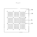
- Fig. 1 shows a plan view of a microwell array chip 1a on which three horizontal and three vertical groups 1c of 10 x 10 microwells 1b are provided.
- a marker 1d is provided on each of the four corners of 10 x 10 microwell groups 1c. It is also possible to provide markers on the four corners of the overall microwell array chip 1a to distinguish the markers provided on the four corners of each group.
- the markers may be used simply to identify position, or may be numbers or letters.
- the use of markers in the form of numbers or letters not only determines the position of each group, but can also specify each group. That is, a number can be assigned to each group.
- the markers may be legible by fluorescence microscope or image scanner, for example. Thus, they are desirably comprised of a fluorescent material or reflective material.
- fluorescent materials are materials emitting fluorescence at a prescribed wavelength when excited by light entering from the exterior.
- a processed substrate material and a thin-film formed on a substrate are selected as reflective materials.
- a reflective structure having an incline relative to the surface or an identification pattern having characters or information can be formed.
- a thin film on the substrate material and fabricating a rise and dip structure by processing such as etching it is possible to form an irregularly reflecting structure based on minute indentations and protrusions on the surface of the thin film or inclines in the edge surfaces of the thin film, achieving the same effect as described above.
- the shape may be one in which a portion of the top of an inverted cone or inverted pyramid is cut off (in which case the bottom of the microwell is flat).
- the bottom of the microwell is normally flat, but curved surfaces (convex or concave) are also possible. The reason the bottom of the microwell is made curved is the same as for shapes consisting of an inverted cone or inverted pyramid with a portion of the top cut off.
- the shape and size of the microwell are suitably determined in consideration of the type of organic cell (shape, size, and the like of the organic cell) to be stored in the microwell so that a single organic cell will be contained per microwell.
- the depth of the microwell suitably falls within a range of 0.5 to 4-fold, desirably 0.8 to 1.9-fold, and preferably, 0.8 to 1.8-fold the diameter of the organic cell to be contained in the microwell.
- the dimensions can be, for example, a diameter of 3 to 100 micrometers.
- the diameter is desirably 4 to 15 micrometers.
- the depth can be from 3 to 100 micrometers, and in the case where the organic cell is a B lymphocyte, the depth is desirably 4 to 40 micrometers.
- the dimensions of the microwell, as set forth above can be suitably determined in consideration of a desirable ratio of the diameter of the organic cell to be contained in the microwell to the dimensions of the microwell.
- the number of microwells present in a single microwell array chip is not specifically limited. However, when the organic cell is a lymphocyte and the frequency of a given antigen-specific lymphocyte per 10 5 cells is from 1 to about 500 at the high end, the number of microwells can range from about 2,000 to 1,000,000 per cm 2 , for example.
- the shape of the surface of the inner wall of the microwell is desirably smooth so as to permit smooth removal of cells.
- the height of dips and rises on the surface can fall within a range of 0 to 1.0 micrometer, preferably a range of 0 to 0.5 micrometer, and more preferably, a range of 0 to 0.1 micrometer.
- the inner wall of a microwell can be smoothed by etching.
- the degree of vacuum in the etching device, the type of etching gas, the etching steps, and the like can be suitably selected.
- the process cycle time of the etching step and the protective film forming step are desirably suitably selected. Smoothing of the inner wall of a microwell can be conducted by wet etching or by combining a hot oxidation step with oxide film etching.
- the process cycle of the device can be varied to form dips and rises of desired height at desired positions on the inner wall of the microwell.
- this can be achieved by suitably selecting the type, concentration, and temperature of the chemical solution.
- Protrusions can also be formed at specific sites on the well sidewall by etching. For example, by extending the process cycle time at a position at which the formation of a protrusion is desired using a Multiplex ASE etching device made by STS Corporation, a protrusion of desired height can be formed at a desired position on the well sidewall. Protrusions can also be formed by suitably selecting and varying the etching conditions at positions at which the formation of protrusions is desired using etching devices other than the above etching device.
- the microwell array chip of Aspect I can be made of silicon, metal, or resin, for example.
- silicon processing technology which is currently the mainstream fabrication technology for semiconductor integrated circuits, can be applied without modification.
- the use of silicon is superior to the use of other materials from the perspectives of microprocessing properties, mass production properties, and integration with future analytical circuits such as sensors.
- Examples of the above metal are aluminum, stainless steel, copper, nickel, chromium, and titanium.
- Examples of the above resin are polyimide, polyethylene, vinyl chloride, polypropylene, polycarbonate, acrylic, and polyethylene terephthalate.
- quantum effects typified by carrier barrier phenomena of electrons and holes, such as photoluminescent structures employing the effects of confined carriers, may be exploited.
- the photoluminescent material employed may be suitably selected based on the wavelength required.
- a photoluminescent structure may be added to the chip, or a photoluminescent structure may be built into the chip itself.
- quantum-effect particles, impurity doping, porous materials, and thin-film lamination-based quantum well structures may be formed or a film of a photoluminescent material may be formed to provide markers on the microwell array chip of Aspect I.
- the microwell array chip of Aspect I may have a hydrophobic region provided in a manner surrounding multiple microwells on a principal surface having multiple microwells.
- Fig. 14 is a schematic diagram of a microwell array chip on which such a region is provided.
- a hydrophobic region is provided in a manner surrounding the microwells so that the solution containing cells and the like being planted on the microwell array does not cross the hydrophobic region and disperse, thereby permitting efficient concentration of the cell dispersion on the microwells.
- Such a region may be flat or may be in the form of a groove. The number of such regions is not specifically limited. A single such region may be provided, or two or more may be provided.
- the width of this region may be suitably established based on the amount of solution being planted; for example, the width may be 100 micrometers to 1 mm.
- the depth of the groove may be suitably set based on the amount of solution being planted; for example, the depth may be 5 to 100 micrometers.
- the hydrophobic region may have a silicon surface or a fluorine-containing surface, for example.
- the formation of wells on and etching of the silicon substrate itself as set forth above can yield a microwell array chip on which are provided groove-like hydrophobic regions, as well as a microwell array chip on which are provided groove-like hydrophobic regions in which the silicon surface has been exposed by oxide film etching.
- An example of a method for manufacturing such a microwell array chip will be described below with reference to Fig. 16 .
- fluorine-containing surfaces may be present.
- fluorine-containing surfaces are: fluorocarbon surfaces; fluororesin surfaces comprised of carbon, fluorine, hydrogen, and the like; and fluorosilicon surfaces.
- the hydrophobic regions having fluorine-containing surfaces can be provided by the methods of stamping, printing, or coating a fluorine-based water repellent; the method of forming a groove by etching, for example, and causing a fluorine-based water repellent to flow into the groove; an inkjet method; or a spraycoating method.
- the hydrophobic regions may also be provided using a silicone resin or paraxylene resins such as parylene. This makes it possible to provide hydrophobic regions even on substrates made of metal or resin.
- the excitation radiation employed in a fluorescence detector is irregularly reflected by reflective structures or an irregularly shaped surface. Since a band-pass filter normally eliminating all but the desired fluorescence wavelength is mounted on the detector, the excitation light fully reflected by the chip surface does not enter the detector. However, irregularly reflected light reflects off a mirror having the properties of an initial stage band-pass filter, and can reach the detector. Accordingly, the band-pass filter before the detector in the rear stage is removed during label identification to allow irregularly reflected light to enter the detector.
- the shape of the label pattern is desirably concave rather than convex to facilitate identification.
- microwell array chip of Aspect II of the present invention multiple microwells are present on a principal surface of a substrate, the microwells are of a shape and size permitting the storage of only a single organic cell in each microwell, and protruding members are present in the openings of the microwells to narrow the openings.
- the protrusions can be formed by causing a film formed on the substrate surface to protrude into the openings.
- the protrusions are not limited to this Aspect. The Aspect of forming the protrusions so that a film provided on the substrate surface protrudes into the openings will be described based on Fig. 7 .
- the shape of the opening formed by the protrusion may differ from that of protrusion 14 in Fig. 7 and that of protrusion 14' in Fig. 8 .
- the size of the opening formed by the protrusion is adequate to allow the passage of the organic cell that is to be stored in the microwell.
- Fig. 9 shows lateral cross-sectional views of microwell array chips of Aspect II with differing microwell shapes.
- Fig. 9(C) which is the same Aspect as in Figs. 7 and 8 , the microwell is an inverted pyramid, while the microwell of Fig. 9(D) is square and that of Fig. 9(E) is hemispherical.
- the shape of the microwell is not specifically limited, and shapes other than these are possible.
- the shape of the microwell can be cylindrical. It can also be noncylindrical, such as a polyhedron comprised of multiple faces (for example, a parallelepiped, hexagonal column, or octagonal column), an inverted cone, an inverted pyramid (inverted triangular pyramid, inverted square pyramid, inverted pentagonal pyramid, inverted hexagonal pyramid, or an inverted polygonal pyramid with seven or more angles), or have a shape combining two or more of these shapes. For example, it may be partly cylindrical, with the remainder having the shape of an inverted cone. In the case of an inverted conical or an inverted pyramidal shape, the mouth of the microwell is on the bottom.
- the shape may be one in which a portion of the top of an inverted cone or inverted pyramid is cut off (in which case the bottom of the microwell is flat).
- the bottom of the microwell is normally flat, but curved surfaces (convex or concave) are also possible. The reason the bottom of the microwell is made curved is the same as for shapes consisting of an inverted cone or inverted pyramid with a portion of the top cut off.
- the shape and size of the microwell are suitably determined in consideration of the type of organic cell (shape, size, and the like of the organic cell) to be stored in the microwell so that a single organic cell will be contained per microwell.
- the diameter of the largest circle that can be inscribed in the planar shape of the opening formed by the protrusion provided in the opening of the microwell suitably falls within a range of 0.5 to 2-fold, desirably 0.8 to 1.9-fold, and preferably, 0.8 to 1.8-fold the diameter of the organic cell to be contained in the microwell.
- the dimensions can be, for example, a diameter of 3 to 100 micrometers.
- the diameter is desirably 4 to 15 micrometers.
- the depth can be from 3 to 100 micrometers, and in the case where the organic cell is a B lymphocyte, the depth is desirably 4 to 40 micrometers.
- the dimensions of the microwell, as set forth above can be suitably determined in consideration of a desirable ratio of the diameter of the organic cell to be contained in the microwell to the dimensions of the microwell.
- the number of microwells present in a single microwell array chip is not specifically limited. However, when the organic cell is a lymphocyte and the frequency of a given antigen-specific lymphocyte per 10 5 cells is from 1 to about 500 at the high end, the number of microwells can range from about 2,000 to 1,000,000 per cm 2 , for example.
- the substrate of the microwell array chip of Aspect II can be made of silicon, metal, or resin, for example.
- silicon processing technology which is currently the mainstream fabrication technology for semiconductor integrated circuits, can be applied without modification.
- the use of silicon is superior to the use of other materials from the perspectives of microprocessing properties, mass production properties, and integration with future analytical circuits such as sensors.
- Examples of the metal constituting the substrate are aluminum, stainless steel, copper, nickel, chromium, and titanium.
- Examples of the resin constituting the substrate are polyimide, polyethylene, vinyl chloride, polypropylene, polycarbonate, acrylic, and polyethylene terephthalate.
- oxide films are silicon oxide films, silicon oxide nitride films, aluminum oxide films, and titanium oxide films.
- nitride films examples include silicon nitride films, aluminum nitride films, and titanium nitride films.
- An example of an impurity diffusion layer is the distribution of a high concentration of boron into a silicon substrate surface.
- metal films are aluminum, gold, platinum, stainless steel, copper, nickel, chromium, titanium, germanium, and silicon germanium.
- the type of film provided on the substrate surface is desirably an oxide film, nitride film, or impurity diffusion layer from the perspective of being able to apply current mainstream integrated circuit fabrication technology as is and in terms of mass production properties, cost reduction, and reliability.
- the film provided on the substrate surface is desirably a resin film from the perspectives of the application of photolithography, etching selection, and mass production properties.
- the film provided on the substrate surface is desirably made of metal from the perspectives of the application of photolithography, combination with sensors, film durability, and mass production properties.
- the film provided on the substrate surface is desirably made of resin from the perspectives of the application of photolithography, etching selection, and the like.
- the film provided on the substrate surface is desirably an oxide film, nitride film, or the like from the perspectives of ease of film formation and durability and adhesion of the film.
- the film provided on the substrate surface is desirably made of resin from the perspectives of cost reduction and the ability to use various known forming and processing techniques in manufacturing.
- the microwell array chip of Aspect II may also have hydrophobic regions provided in such a manner as to surround the multiple microwells on the principal surface having multiple microwells. The specific details of these regions are as described for Aspect 1 above.
- the microwell array chip of Aspect III of the present invention is a microwell array chip made of silicon and having multiple microwells, each microwell being used to store a single specimen organic cell, wherein each microwell is of a size and shape capable of holding just one organic cell.
- the above specimen organic cell can be a lymphocyte, for example.
- the microwell array chip of the present invention can be used to detect individual antigen-specific lymphocytes.
- the shape of the microwell can be cylindrical. It can also be noncylindrical, such as a polyhedron comprised of multiple faces (for example, a parallelepiped, hexagonal column, or octagonal column), an inverted cone, an inverted pyramid (inverted triangular pyramid, inverted square pyramid, inverted pentagonal pyramid, inverted hexagonal pyramid, or an inverted polygonal pyramid with seven or more angles), or have a shape combining two or more of these shapes. For example, it may be partly cylindrical, with the remainder having the shape of an inverted cone. In the case of an inverted conical or an inverted pyramidal shape, the mouth of the microwell is on the bottom.
- the shape may be one in which a portion of the top of an inverted cone or inverted pyramid is cut off (in which case the bottom of the microwell is flat).
- the bottom of the microwell is normally flat, but curved surfaces (convex or concave) are also possible. The reason the bottom of the microwell is made curved is the same as for shapes consisting of an inverted cone or inverted pyramid with a portion of the top cut off.
- the shape and size of the microwell are suitably determined in consideration of the type of organic cell (shape, size, and the like of the organic cell) to be stored in the microwell so that a single organic cell will be contained per microwell.
- the diameter of the largest circle that can be inscribed in the planar shape of the microwell suitably falls within a range of 0.5 to 2-fold, desirably 0.8 to 1.9-fold, and preferably, 0.8 to 1.8-fold the diameter of the organic cell to be contained in the microwell.
- the depth of the microwell suitably falls within a range of 0.5 to 4-fold, desirably 0.8 to 1.9-fold, and preferably, 0.8 to 1.8-fold the diameter of the organic cell to be contained in the microwell.
- the dimensions can be, for example, a diameter of 3 to 100 micrometers.
- the diameter is desirably 4 to 15 micrometers.
- the depth can be from 3 to 100 micrometers, and in the case where the organic cell is a B lymphocyte, the depth is desirably 4 to 40 micrometers.
- the dimensions of the microwell, as set forth above can be suitably determined in consideration of a desirable ratio of the diameter of the organic cell to be contained in the microwell to the dimensions of the microwell.
- the number of microwells present in a single microwell array chip is not specifically limited. However, when the organic cell is a lymphocyte and the frequency of a given antigen-specific lymphocyte per 10 5 cells is from 1 to about 500 at the high end, the number of microwells can range from about 2,000 to 1,000,000 per cm 2 , for example.
- the shape of the surface of the inner wall of the microwell in Aspect III is desirably smooth so as to permit smooth removal of cells.
- the specific details are as described for Aspect I.
- the microwell array chip of Aspect III of the present invention is made of silicon.
- the use of silicon permits the application as is of the silicon processing techniques that are the mainstream of current semiconductor integrated circuit manufacturing techniques.
- silicon is better than other materials in terms of its micromanufacturing properties, mass production properties, and future integration with analysis circuits, including sensors.
- microwell array chip of Aspect III is made of silicon
- the fact that a film of silicon oxide covers the substrate surface is desirable from the perspectives of the hydrophilic property of the chip surface, the stability of the film, and mass production properties.
- a silicon surface is normally hydrophobic, having the property of repelling cell suspension solution during planting of the cell suspension solution and sometimes impeding the storage of organic cells in the microwells. Accordingly, a silicon oxide film is desirable from the perspectives of having a greater hydrophilic property than silicon and affording film stability.
- the inner surface of the microwells is desirably covered with a fluorocarbon film or silicon oxide film.
- a fluorocarbon film or silicon oxide film Forming an inert, exclusive surface such as a fluorocarbon film or silicon oxide film on the inner surface of the microwells is desirable in that it prevents adhesion of the organic cell and facilitates recovery of the organic cell from the microwell.
- Fluorocarbon films are water-repellent films.
- a water-repellent film is desirably formed only within the wells; the formation of a silicon oxide film (silicon oxide film) such as that set forth above is desirable on surfaces other than the wells of the microwell array chip.
- silicon oxide films do not exhibit a water-repellent property such as that of fluorocarbon films, they have an effect in preventing the adhesion of organic cells.
- silicon oxide films formed by high-temperature oxidation with dry oxygen are dense. Although they do not have water repellency to the degree of beading water like fluorocarbon films, they have a property that is between a hydrophilic and a hydrophobic property.
- surfaces other than well surfaces are desirably coated with silicon oxide films, and fluorocarbon films or silicon oxide films are desirably selectively formed just in the wells.
- the film is formed after the well has been fabricated.
- the entire substrate ends up being covered by the fluorocarbon film, becoming a water-repellent surface. Accordingly, the following method is employed in the present invention. This method will be described for the example of a microwell array chip employing a silicon substrate.
- a microwell pattern is formed by photolithography on a silicon substrate.
- the photoresist hardening temperature is not greater than 100°C.
- a dry etching vacuum device is employed to form the microwells.
- a CF-based gas is introduced into the vacuum device and plasma CVD is conducted.
- the plasma CVD can be conducted using the etching device as is, or in the CVD device of a separate body of equipment.
- the substrate is removed from the vacuum device and immersed in an organic solvent such as methanol or acetone. This lifts off both the microwell pattern mask and the fluorocarbon film on it, leaving a fluorocarbon film only on the inner wall of the microwell.
- the etching and film forming steps can be conducted in the same device by simply changing the type of gas employed.
- the inner surface of the wells can be coated with a silicon oxide film, as set forth above.
- An improved effect on the recovery rate of organic cells from the wells can be achieved even when the inner surface of the wells is covered with a silicon oxide film instead of a fluorocarbon film.
- porous silicon can be produced by a method such as anodizing the inner surface of the wells.
- the microwell array chip of the present invention can be treated, or a film can be formed, to inhibit active silicon surfaces.
- hydrophobic regions can be provided in a manner surrounding multiple microwells on a surface having multiple microwells.
- the specific details of these hydrophobic regions are as set forth above in Aspect I.
- such regions may also be coated with a fluorocarbon film to form hydrophobic regions in the course of coating the inner surface of the microwells with a fluorocarbon film.
- Fig. 1 is an example of a Aspect of implementing the device of Aspect I of the present invention.
- One use of the present microwell array chip is the introduction of a cell to which a fluorescent substance has been added into each well for evaluation, and the determination of fluorescent emission. In this process, those cells not emitting fluorescence cannot be observed because observation by fluorescence microscope or fluorescence scanner is conducted with specifications based on the wavelength of fluorescence. Accordingly, as shown in Fig. 1 , a minute marker 1d of a fluorescent substance is formed between the individual clusters.
- the photoresist does not denature and become difficult to remove in the dry etching step. Further, the silicon substrate surface that is formed yields an ultrahydrophilic surface due to a plasma effect.
- the above steps readily produce a shape such as that shown in Fig. 2 .
- the pattern of marker 2c may be freely selected from among designs, codes, characters, and the like. It is also possible to display information other than markers on the microchip.
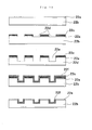
- Fig. 3 is an implementation Aspect of a reflective marker 3d that is observable by observing scattered light with a fluorescence microscope or fluorescence scanner by forming dips and rises on silicon substrate 3a. It is used as a marker for identifying the positions of clusters of multiple microwells 3b arrayed on silicon substrate 3a.
- indentation 3e By forming indentation 3e by etching or the like on the substrate and directing a fluorescence excitation beam to an observation device by means of irregular reflection, it is possible to identify the position of the indentation.
- the bottom of indentation 4b is desirably an inverted pyramid.
- microwell array chip with reflection markers An example of manufacturing a microwell array chip with reflection markers will be described for the case of a silicon substrate based on Figs. 5 and 6 .
- Fig. 7 shows a microwell structure fabricated based on Aspect II of the present invention.
- the microwell array chip of Aspect II may also have the structures shown in Figs. 9(D) and (E) .
- An array chip having microwells of the structures shown in Figs. 9(D) and (E) can be formed by varying the above method as follows.
- the structure of Fig. 9(D) can be achieved by RIE dry etching and suitably selecting a substrate surface orientation and well pattern. For example, face (100), (110), or (111) is selected as the substrate face orientation and a pattern shape that will cause an etching face to appear that is perpendicular to the substrate surface can be selected.
- the structure of Fig. 9(E) can be achieved by an etching method with isotropic etching characteristics. For example, in common dry etching and etching with a mixed solution of hydrofluoric acid and nitric acid, the silicon etches isotropically, readily yielding the structure of Aspect II of the present invention.
- the thin film layer is not limited to an oxide film.
- a switch to high impurity concentration diffused silicon, germanium, silicon germanium, metal thin films, resins, and the like is also possible. Either wet etching or dry etching may be employed. Since wet etching permits the processing of substrates in batches, it affords good mass production efficiency.
- the array (fill) rate increased with the depth of the well, but with a large opening such as that of sample B, the array (fill) rate tended to decrease. Accordingly, the design of the well must suitably take into account the depth, opening diameter, and eave dimension of the well.
- Fig. 11 is a schematic drawing descriptive of a microwell array chip relating to Aspect III of the present invention.
- microwell patterns 21b are arranged on the surface of silicon substrate 21a.
- the size of each microwell 21b is from several micrometers to several tens of micrometers.
- a fluorocarbon film 21c was formed with a CxFy-based gas on the sidewall of each well formed, and a surface energy reducing effect created an inert state. Fluorocarbon film 21c, which exhibited a hydrophobic property, was selectively formed within the microwells, but was not present on the outermost surface 21d of the silicon. The organic cell entering microwell 21b tended not to readily adhere. The effect of providing a fluorocarbon film inside the microwells was particularly marked when the microwell was deep.
- Fig. 12 shows the steps of manufacturing a microwell array chip employing a silicon substrate.
- the array (fill) rate of a microwell array chip obtained by the above-described method was evaluated by the same method as in Embodiment 3.
- the collection rate was evaluated by the following method.
- the results are given in Table 2.
- Table 2 gives the evaluation results for a microwell array chip in which a fluorocarbon film was formed within the wells. The same well diameter and depth were selected for all of the samples.
- the concentration of the planted cells was 10 5 cells/microliter.
- Embodiment 4 the inner walls of the microwell array chip were treated for smoothness prior to formation of the fluorocarbon film.
- the smoothness treatment was conducted using a Multiplex ASE etching device made by STS Corporation and adjusting the process cycle times of the etching step and protective film formation step.
- two types of microwell array chips were manufactured: one having dips and rises 0.5 micrometer in height on the inner walls, and the other having dips and rises 0.1 micrometer in height on the inner walls.
- Fig. 17 is an enlarged photograph of microwells having dips and rises 0.1 micrometer in height on the inner walls.
- Embodiment 4 protrusions 0.6 micrometer in height were formed in the openings of the microwells. Using a Multiplex ASE etching device made by STS Corporation, the process cycle time of the device was extended during initial etching to form protrusions of desired height. Following the formation of protrusions, the process cycle time was adjusted to manufacture microwells having protrusions only in the openings. Fig. 18 is an enlarged photograph of microwells in which protrusions have been formed in the openings.
- Protrusions can be formed at any position.
- the process cycle time can be adjusted at a position where the formation of a protrusion is desired to make a protrusion in the middle of the well, on the bottom of the well, or anywhere else. Suitable selection of the shape and number of protrusions can be anticipated to yield a variety of effects.
- markers in the form of a fluorescent substance, reflective structures, or the like are present at targeted locations. These markers function to identify positions, thereby facilitating the identification of positions by fluorescence microscope.
- microwell positions can be readily determined by fluorescence microscope, image scanner, or the like.
- a single specific specimen of an organic cell stored in an individual microwell - for example, an antigen-specific lymphocyte - can be readily specified.
- a cell that has entered a well catches on the protrusion (eave) at the top of the well, it can be retained in the well with high probability and not flow to the exterior of the well during washing.
- the formation of a lip changes the distribution of fluid on the chip surface and within the well.
- a cell that has already entered can be prevented from flowing out with the liquid during washing.
- the shape of the well can prevent the generation of a vacuum between the cell and the well surface during suction. That is, when the well is imparted with the shape of an inverted pyramid, the ridgelines function to relieve pressure so that during aspiration of the cell, no vacuum forms between the well and the cell, permitting ready collection of the cell.
- an antigen-specific lymphocyte that has been detected can be removed and the antigen-specific antibody gene or T cell receptor gene can be cloned.
- the antigen-specific antibody gene or T cell receptor gene can be cloned.
- the antigen-specific antibody gene it can be used to produce large amounts of human monoclonal antibody. It is thought that this antibody can then be administered to patients with an infectious disease or the like to treat and prevent the infectious disease or the like.
Applications Claiming Priority (4)
| Application Number | Priority Date | Filing Date | Title |
|---|---|---|---|
| JP2003333363 | 2003-09-25 | ||
| JP2003336771 | 2003-09-29 | ||
| JP2003336793 | 2003-09-29 | ||
| EP04773462A EP1691196B1 (fr) | 2003-09-25 | 2004-09-22 | Puce de reseau de micropuits et son procede de fabrication |
Related Parent Applications (1)
| Application Number | Title | Priority Date | Filing Date |
|---|---|---|---|
| EP04773462.9 Division | 2004-09-22 |
Publications (1)
| Publication Number | Publication Date |
|---|---|
| EP2381255A1 true EP2381255A1 (fr) | 2011-10-26 |
Family
ID=34799286
Family Applications (2)
| Application Number | Title | Priority Date | Filing Date |
|---|---|---|---|
| EP04773462A Active EP1691196B1 (fr) | 2003-09-25 | 2004-09-22 | Puce de reseau de micropuits et son procede de fabrication |
| EP11160721A Withdrawn EP2381255A1 (fr) | 2003-09-25 | 2004-09-22 | Puce de reseau de micropuits et son procédé de fabrication |
Family Applications Before (1)
| Application Number | Title | Priority Date | Filing Date |
|---|---|---|---|
| EP04773462A Active EP1691196B1 (fr) | 2003-09-25 | 2004-09-22 | Puce de reseau de micropuits et son procede de fabrication |
Country Status (9)
| Country | Link |
|---|---|
| US (2) | US20080014631A1 (fr) |
| EP (2) | EP1691196B1 (fr) |
| JP (1) | JP4069171B2 (fr) |
| KR (1) | KR101111231B1 (fr) |
| CN (1) | CN102928584B (fr) |
| CA (1) | CA2544470C (fr) |
| DK (1) | DK1691196T3 (fr) |
| ES (1) | ES2411104T3 (fr) |
| WO (1) | WO2005069001A1 (fr) |
Cited By (1)
| Publication number | Priority date | Publication date | Assignee | Title |
|---|---|---|---|---|
| US8772049B2 (en) | 2005-09-16 | 2014-07-08 | President And Fellows Of Harvard College | Screening assays and methods |
Families Citing this family (99)
| Publication number | Priority date | Publication date | Assignee | Title |
|---|---|---|---|---|
| IL154677A0 (en) | 2003-02-27 | 2003-09-17 | Univ Bar Ilan | A method and apparatus for manipulating an individual cell |
| US8597597B2 (en) | 2003-06-26 | 2013-12-03 | Seng Enterprises Ltd. | Picoliter well holding device and method of making the same |
| US9200245B2 (en) | 2003-06-26 | 2015-12-01 | Seng Enterprises Ltd. | Multiwell plate |
| US7888110B2 (en) | 2003-06-26 | 2011-02-15 | Seng Enterprises Ltd. | Pico liter well holding device and method of making the same |
| ES2352344T3 (es) | 2005-01-25 | 2011-02-17 | Seng Enterprises Limited | Dispositivo de microfluido para estudio de células. |
| JP4711125B2 (ja) * | 2005-09-27 | 2011-06-29 | 横河電機株式会社 | バイオチップ、バイオチップ読み取り装置、およびバイオチップ読み取り方法 |
| WO2007046582A1 (fr) * | 2005-10-21 | 2007-04-26 | Korea Research Institute Of Bioscience And Biotechnology | Procede pour fabriquer un nano-intervalle et capteur de nano-intervalle |
| KR100849384B1 (ko) | 2005-10-21 | 2008-07-31 | 한국생명공학연구원 | 나노갭 및 나노갭 센서의 제조방법 |
| WO2007052245A1 (fr) | 2005-11-03 | 2007-05-10 | Seng Enterprises Ltd. | Procédé et dispositif d’étude de cellules vivantes flottantes |
| US7974003B2 (en) * | 2006-11-22 | 2011-07-05 | Vanderbilt University | Photolithographed micro-mirror well for 3D tomogram imaging of individual cells |
| JP5041473B2 (ja) * | 2007-03-06 | 2012-10-03 | 国立大学法人山口大学 | 蛍光テストチャート |
| WO2008157640A2 (fr) * | 2007-06-18 | 2008-12-24 | Illumina, Inc. | Procédés de microfabrication pour le modelage optimal de substrats |
| JP4148367B1 (ja) | 2007-08-02 | 2008-09-10 | 富山県 | 細胞のスクリーニング方法 |
| WO2009057792A1 (fr) * | 2007-10-31 | 2009-05-07 | Arkray, Inc. | Instrument d'analyse |
| US9145540B1 (en) | 2007-11-15 | 2015-09-29 | Seng Enterprises Ltd. | Device for the study of living cells |
| WO2009081409A2 (fr) | 2007-12-26 | 2009-07-02 | Seng Enterprises Ltd. | Dispositif pour l'étude de cellules vivantes |
| US8680023B2 (en) * | 2008-08-21 | 2014-03-25 | International Business Machines Corporation | Methods for screening and arraying microrganisms such as viruses using subtractive contact printing background |
| EP2336348B1 (fr) * | 2008-09-02 | 2014-11-05 | National Institute of Advanced Industrial Science And Technology | Procédé de détection de cellule et puce à adn destinée à être utilisée dans ledit procédé |
| JP2010151525A (ja) * | 2008-12-24 | 2010-07-08 | Seiko Epson Corp | 反応場を有するデバイス |
| US20100204057A1 (en) * | 2009-02-10 | 2010-08-12 | Samsung Electronics Co., Ltd. | Substrate for microarray, method of manufacturing microarray using the same and method of obtaining light data from microarray |
| EP2219027A1 (fr) * | 2009-02-12 | 2010-08-18 | Centre National de la Recherche Scientifique | Dispositifs et procédés pour observer la division cellulaire |
| WO2010107497A2 (fr) * | 2009-03-18 | 2010-09-23 | The Regents Of The University Of California | Puits de rétrécissement en nid d'abeille pour la culture de cellules souches |
| US20120302462A1 (en) | 2009-11-09 | 2012-11-29 | Bjorn Onfelt | System and Method for Detecting and Quantifying Active T-cells or Natural Killer Cells |
| KR101144064B1 (ko) * | 2009-12-09 | 2012-05-23 | (주)유 바이오메드 | 마이크로어레이 칩 및 그의 제조방법 |
| JP5771962B2 (ja) * | 2010-12-08 | 2015-09-02 | 大日本印刷株式会社 | マイクロ流路チップ及びその製造方法 |
| CN102117738B (zh) * | 2010-12-31 | 2013-04-03 | 中微半导体设备(上海)有限公司 | 使用含碳氟化合物的聚合物使硅片顶角圆化的方法 |
| CN103477433A (zh) | 2011-06-22 | 2013-12-25 | 松下电器产业株式会社 | 具有点标记的半导体基板及其制造方法 |
| JP2014518080A (ja) | 2011-06-27 | 2014-07-28 | バルネバ | 細胞のスクリーニング方法 |
| JP2013047625A (ja) * | 2011-08-29 | 2013-03-07 | Sumitomo Bakelite Co Ltd | マルチウェルプレート |
| US10752949B2 (en) | 2012-08-14 | 2020-08-25 | 10X Genomics, Inc. | Methods and systems for processing polynucleotides |
| WO2014028537A1 (fr) | 2012-08-14 | 2014-02-20 | 10X Technologies, Inc. | Compositions de microcapsule et procédés |
| US10221442B2 (en) | 2012-08-14 | 2019-03-05 | 10X Genomics, Inc. | Compositions and methods for sample processing |
| US10584381B2 (en) | 2012-08-14 | 2020-03-10 | 10X Genomics, Inc. | Methods and systems for processing polynucleotides |
| US10273541B2 (en) | 2012-08-14 | 2019-04-30 | 10X Genomics, Inc. | Methods and systems for processing polynucleotides |
| US10323279B2 (en) | 2012-08-14 | 2019-06-18 | 10X Genomics, Inc. | Methods and systems for processing polynucleotides |
| US9701998B2 (en) | 2012-12-14 | 2017-07-11 | 10X Genomics, Inc. | Methods and systems for processing polynucleotides |
| US9951386B2 (en) | 2014-06-26 | 2018-04-24 | 10X Genomics, Inc. | Methods and systems for processing polynucleotides |
| US11591637B2 (en) | 2012-08-14 | 2023-02-28 | 10X Genomics, Inc. | Compositions and methods for sample processing |
| CA2894694C (fr) | 2012-12-14 | 2023-04-25 | 10X Genomics, Inc. | Procedes et systemes pour le traitement de polynucleotides |
| US10533221B2 (en) | 2012-12-14 | 2020-01-14 | 10X Genomics, Inc. | Methods and systems for processing polynucleotides |
| EP3862435A1 (fr) | 2013-02-08 | 2021-08-11 | 10X Genomics, Inc. | Génération de codes à barres de polynucléotides |
| US20160018428A1 (en) * | 2013-03-15 | 2016-01-21 | Douglas Scientific, LLC | Reusable belt with a matrix of wells |
| JP2015010910A (ja) * | 2013-06-28 | 2015-01-19 | 株式会社ニコン | 検出方法、検出装置、バイオチップのスクリーニング方法、スクリーニング装置及びバイオチップ |
| JP2015017940A (ja) * | 2013-07-12 | 2015-01-29 | 株式会社ニコン | 検出方法、検出装置、バイオチップのスクリーニング方法、スクリーニング装置及びバイオチップ |
| US10395758B2 (en) | 2013-08-30 | 2019-08-27 | 10X Genomics, Inc. | Sequencing methods |
| JP5920375B2 (ja) * | 2013-09-11 | 2016-05-18 | 大日本印刷株式会社 | 細胞培養容器 |
| JP6330278B2 (ja) * | 2013-09-11 | 2018-05-30 | 大日本印刷株式会社 | 培養容器 |
| JP6277639B2 (ja) * | 2013-09-11 | 2018-02-14 | 大日本印刷株式会社 | 培養容器 |
| JP6303347B2 (ja) | 2013-09-11 | 2018-04-04 | 大日本印刷株式会社 | 検体画像管理システム及び検体画像管理プログラム |
| US9824068B2 (en) | 2013-12-16 | 2017-11-21 | 10X Genomics, Inc. | Methods and apparatus for sorting data |
| JP2015194379A (ja) * | 2014-03-31 | 2015-11-05 | 株式会社ニコン | バイオチップ及びバイオチップにおけるアライメントマークの検出方法 |
| AU2015243445B2 (en) | 2014-04-10 | 2020-05-28 | 10X Genomics, Inc. | Fluidic devices, systems, and methods for encapsulating and partitioning reagents, and applications of same |
| JP2017518752A (ja) * | 2014-06-12 | 2017-07-13 | ウエハージェン インコーポレイテッド | 捕捉用重合体膜を用いた単細胞捕捉 |
| KR20170023979A (ko) | 2014-06-26 | 2017-03-06 | 10엑스 제노믹스, 인크. | 핵산 서열 조립을 위한 프로세스 및 시스템 |
| CN106795553B (zh) | 2014-06-26 | 2021-06-04 | 10X基因组学有限公司 | 分析来自单个细胞或细胞群体的核酸的方法 |
| CA2964472A1 (fr) | 2014-10-29 | 2016-05-06 | 10X Genomics, Inc. | Procedes et compositions de sequencage cible d'acides nucleiques |
| US9975122B2 (en) | 2014-11-05 | 2018-05-22 | 10X Genomics, Inc. | Instrument systems for integrated sample processing |
| EP3244992B1 (fr) | 2015-01-12 | 2023-03-08 | 10X Genomics, Inc. | Procédés de codage a barres d'acides nucléiques |
| JP2018508852A (ja) | 2015-01-13 | 2018-03-29 | 10エックス ゲノミクス,インコーポレイテッド | 構造的変異及び相化情報を視覚化するシステム及び方法 |
| MX2017010142A (es) | 2015-02-09 | 2017-12-11 | 10X Genomics Inc | Sistemas y metodos para determinar variacion estructural y ajuste de fases con datos de recuperacion de variantes. |
| BR112017018054A2 (pt) | 2015-02-24 | 2018-07-24 | 10X Genomics Inc | métodos para a cobertura de sequências de ácidos nucleicos direcionadas |
| EP3262407B1 (fr) | 2015-02-24 | 2023-08-30 | 10X Genomics, Inc. | Procédés et systèmes de traitement de cloisonnement |
| JP2016174578A (ja) * | 2015-03-20 | 2016-10-06 | 東ソー株式会社 | 微小粒子選別装置および前記装置を備えた微小粒子回収装置 |
| CN107430142B (zh) * | 2015-03-31 | 2020-01-14 | 东丽株式会社 | 分析用芯片 |
| WO2017062807A1 (fr) * | 2015-10-07 | 2017-04-13 | Arizona Board Of Regents On Behalf Of Arizona State University | Procédé d'ensemencement de cellules vivantes pour microréseaux |
| SG10202108763UA (en) | 2015-12-04 | 2021-09-29 | 10X Genomics Inc | Methods and compositions for nucleic acid analysis |
| JP2017108738A (ja) * | 2015-12-15 | 2017-06-22 | 東ソー株式会社 | 細胞検出装置および細胞回収装置 |
| SG11201806757XA (en) | 2016-02-11 | 2018-09-27 | 10X Genomics Inc | Systems, methods, and media for de novo assembly of whole genome sequence data |
| US20190126043A1 (en) * | 2016-04-14 | 2019-05-02 | The Trustees Of The University Of Pennsylvania | Implantable living electrodes and methods for use thereof |
| EP3445490B1 (fr) | 2016-04-22 | 2022-06-29 | Becton, Dickinson and Company | Dépôt à haute densité pour la production de réseaux |
| WO2017197338A1 (fr) | 2016-05-13 | 2017-11-16 | 10X Genomics, Inc. | Systèmes microfluidiques et procédés d'utilisation |
| GB201610426D0 (en) * | 2016-06-15 | 2016-07-27 | Q-Linea Ab | Sample holder for image based analysis of samples |
| US10550429B2 (en) | 2016-12-22 | 2020-02-04 | 10X Genomics, Inc. | Methods and systems for processing polynucleotides |
| US10011872B1 (en) | 2016-12-22 | 2018-07-03 | 10X Genomics, Inc. | Methods and systems for processing polynucleotides |
| US10815525B2 (en) | 2016-12-22 | 2020-10-27 | 10X Genomics, Inc. | Methods and systems for processing polynucleotides |
| JP2020043764A (ja) * | 2016-12-28 | 2020-03-26 | Agcテクノグラス株式会社 | 細胞培養基材及びその製造方法 |
| WO2018140966A1 (fr) | 2017-01-30 | 2018-08-02 | 10X Genomics, Inc. | Procédés et systèmes de codage à barres de cellules individuelles sur la base de gouttelettes |
| CN109415674B (zh) * | 2017-03-10 | 2021-10-26 | 株式会社村田制作所 | 细胞过滤滤除器 |
| JP7063541B2 (ja) * | 2017-03-31 | 2022-05-09 | 住友理工株式会社 | 流体デバイス用シリコーン部材およびその製造方法 |
| WO2018213774A1 (fr) | 2017-05-19 | 2018-11-22 | 10X Genomics, Inc. | Systèmes et procédés d'analyse d'ensembles de données |
| US10844372B2 (en) | 2017-05-26 | 2020-11-24 | 10X Genomics, Inc. | Single cell analysis of transposase accessible chromatin |
| SG11201901822QA (en) | 2017-05-26 | 2019-03-28 | 10X Genomics Inc | Single cell analysis of transposase accessible chromatin |
| SG11201913654QA (en) | 2017-11-15 | 2020-01-30 | 10X Genomics Inc | Functionalized gel beads |
| US10829815B2 (en) | 2017-11-17 | 2020-11-10 | 10X Genomics, Inc. | Methods and systems for associating physical and genetic properties of biological particles |
| WO2019123227A1 (fr) * | 2017-12-21 | 2019-06-27 | Politecnico Di Milano | Dispositif médical implantable |
| SG11202009889VA (en) | 2018-04-06 | 2020-11-27 | 10X Genomics Inc | Systems and methods for quality control in single cell processing |
| JP2018124289A (ja) * | 2018-04-10 | 2018-08-09 | 株式会社ニコン | バイオチップ及びバイオチップにおけるアライメントマークの検出方法 |
| US20190345429A1 (en) * | 2018-05-08 | 2019-11-14 | Lidong Qin | Cell Holding Device for Microinjection |
| JPWO2020054559A1 (ja) * | 2018-09-10 | 2021-09-16 | セントラル硝子株式会社 | 含フッ素樹脂組成物 |
| CN109016275B (zh) * | 2018-09-19 | 2024-01-30 | 中国科学院生态环境研究中心 | 微孔模具及其制备方法和应用 |
| KR102170803B1 (ko) | 2018-10-19 | 2020-10-27 | 주식회사 이지다이아텍 | 세포의 격리 및 형태학적 분석 방법 |
| EP3933412A4 (fr) * | 2019-03-01 | 2022-04-06 | Toppan Printing Co., Ltd. | Dispositif microfluidique et procédé d'analyse d'échantillon |
| WO2021002388A1 (fr) * | 2019-07-02 | 2021-01-07 | 旭化成株式会社 | Film à micropuits pour essai biologique, composition de résine photosensible pour former un film à micropuits pour essai biologique, et procédé de fabrication de film à micropuits pour essai biologique |
| CN110596375B (zh) * | 2019-10-17 | 2022-12-27 | 清华大学深圳国际研究生院 | 微孔板、基于微孔板的高灵敏度免疫荧光检测方法 |
| KR102293716B1 (ko) * | 2019-12-26 | 2021-08-26 | 울산과학기술원 | 양면성 구조를 가진 마이크로웰 어레이의 미생물 추출방법 |
| KR102293714B1 (ko) * | 2019-12-26 | 2021-08-26 | 울산과학기술원 | 소수성-친수성 표면을 갖는 마이크로웰 어레이 제조방법, 이에 의해 제조된 마이크로웰 어레이 및 소수성-친수성 표면을 갖는 마이크로웰 어레이의 미생물 현탁액 구획방법 |
| KR102573402B1 (ko) * | 2021-03-24 | 2023-09-04 | 재단법인대구경북과학기술원 | 액체생검 유래 생체물질 분석용 기판, 이의 제조방법 및 이를 이용한 분석방법 |
| CN113866145A (zh) * | 2021-09-26 | 2021-12-31 | 联合基因生物科技(上海)有限公司 | 一种快速聚合酶链式反应用硅基芯片的制造方法 |
| CN114350514B (zh) * | 2021-12-28 | 2024-01-05 | 上海前瞻创新研究院有限公司 | 一种多细胞链状培养装置及其在制备肝索结构中的应用 |
Citations (2)
| Publication number | Priority date | Publication date | Assignee | Title |
|---|---|---|---|---|
| US4395348A (en) * | 1981-11-23 | 1983-07-26 | Ekc Technology, Inc. | Photoresist stripping composition and method |
| EP1119035A2 (fr) * | 2000-01-18 | 2001-07-25 | Applied Materials, Inc. | Méthode de dépôt d'une couche diélectrique à faible constant diélectrique |
Family Cites Families (30)
| Publication number | Priority date | Publication date | Assignee | Title |
|---|---|---|---|---|
| US5272081A (en) * | 1982-05-10 | 1993-12-21 | Bar-Ilan University | System and methods for cell selection |
| US5310674A (en) * | 1982-05-10 | 1994-05-10 | Bar-Ilan University | Apertured cell carrier |
| IL68507A (en) | 1982-05-10 | 1986-01-31 | Univ Bar Ilan | System and methods for cell selection |
| DE3683956D1 (de) * | 1985-06-11 | 1992-04-02 | Us Commerce | In einem serumfreien medium in suspension kultivierte humane monozyten. |
| EP0258565A3 (fr) * | 1986-07-02 | 1989-05-24 | E.I. Du Pont De Nemours And Company | Moyen pour l'identification de la position |
| JPH05240869A (ja) * | 1992-02-28 | 1993-09-21 | Suzuki Motor Corp | 血液等の凝集パターン出力装置 |
| US6410252B1 (en) * | 1995-12-22 | 2002-06-25 | Case Western Reserve University | Methods for measuring T cell cytokines |
| US6156389A (en) * | 1997-02-03 | 2000-12-05 | Cytonix Corporation | Hydrophobic coating compositions, articles coated with said compositions, and processes for manufacturing same |
| US6548263B1 (en) * | 1997-05-29 | 2003-04-15 | Cellomics, Inc. | Miniaturized cell array methods and apparatus for cell-based screening |
| US6232066B1 (en) * | 1997-12-19 | 2001-05-15 | Neogen, Inc. | High throughput assay system |
| US6893877B2 (en) * | 1998-01-12 | 2005-05-17 | Massachusetts Institute Of Technology | Methods for screening substances in a microwell array |
| US6565813B1 (en) * | 1998-02-04 | 2003-05-20 | Merck & Co., Inc. | Virtual wells for use in high throughput screening assays |
| US6210910B1 (en) * | 1998-03-02 | 2001-04-03 | Trustees Of Tufts College | Optical fiber biosensor array comprising cell populations confined to microcavities |
| US6087103A (en) * | 1998-03-04 | 2000-07-11 | Lifespan Biosciences, Inc. | Tagged ligand arrays for identifying target-ligand interactions |
| ATE227338T1 (de) * | 1998-03-18 | 2002-11-15 | Massachusetts Inst Technology | Vaskularisierte perfundierte anordnungen für mikrogewebe und mikroorgane |
| JP4389039B2 (ja) * | 1998-04-09 | 2009-12-24 | 株式会社リンフォテック | アロジェニックな活性化cd4陽性細胞を主成分とする医薬組成物、およびその製造方法、ならびに該医薬組成物調製用キット |
| US20030027214A1 (en) * | 1999-02-17 | 2003-02-06 | Kamb Carl Alexander | Methods for substrate-ligand interaction screening |
| DE19935643A1 (de) * | 1999-07-29 | 2001-02-01 | Augustinus Bader | Vorrichtung zum Züchten und/oder Behandeln von Zellen |
| WO2001062895A2 (fr) * | 2000-02-24 | 2001-08-30 | Xcyte Therapies, Inc. | Stimulation et concentration simultanees de cellules |
| US6734000B2 (en) * | 2000-10-12 | 2004-05-11 | Regents Of The University Of California | Nanoporous silicon support containing macropores for use as a bioreactor |
| US7211209B2 (en) * | 2000-11-08 | 2007-05-01 | Surface Logix, Inc. | Method of making device for arraying biomolecules and for monitoring cell motility in real-time |
| KR20020086625A (ko) * | 2001-01-09 | 2002-11-18 | 마쯔시다덴기산교 가부시키가이샤 | 세포외 전위 측정용 디바이스, 그것을 사용한 세포외 전위측정 방법 및 그것을 구비한 고속 약품 스크리닝 장치 |
| JP4755368B2 (ja) * | 2001-07-24 | 2011-08-24 | 株式会社セルシード | 高密度細胞アレイ用基板、製造法、及びその利用方法 |
| US7169577B2 (en) * | 2001-07-27 | 2007-01-30 | Surface Logix, Inc. | Cell isolation and screening device and method of using same |
| JP4754746B2 (ja) * | 2001-09-28 | 2011-08-24 | オリンパス株式会社 | 棒状担体およびこれを具備するシリンダー反応容器 |
| ATE536548T1 (de) * | 2002-11-14 | 2011-12-15 | Vivalis | Mikrowell-array-chip zum nachweis eines antigenspezifischen lymphozyten, verfahren zum nachweis eines antigenspezifischen lymphozyten und verfahren zur klonierung eines antigenrezeptorgens eines antigenspezifischen lymphozyten |
| CN100347296C (zh) | 2003-03-28 | 2007-11-07 | 财团法人富山县新世纪产业机构 | 使用单个抗原特异性b淋巴细胞制备产生抗原特异性抗体的杂交瘤的方法以及单克隆抗体的制备方法 |
| US20050112033A1 (en) * | 2003-09-08 | 2005-05-26 | Irm, Llc | Multi-well containers, systems, and methods of using the same |
| US20050220675A1 (en) * | 2003-09-19 | 2005-10-06 | Reed Mark T | High density plate filler |
| JP2006105803A (ja) * | 2004-10-06 | 2006-04-20 | Hitachi High-Technologies Corp | 生体試料物質の分析方法、分析装置、マイクロアレイ及びイムノアッセイ |
-
2004
- 2004-09-22 WO PCT/JP2004/014285 patent/WO2005069001A1/fr active Application Filing
- 2004-09-22 DK DK04773462.9T patent/DK1691196T3/da active
- 2004-09-22 CA CA2544470A patent/CA2544470C/fr active Active
- 2004-09-22 KR KR1020067007902A patent/KR101111231B1/ko active IP Right Grant
- 2004-09-22 ES ES04773462T patent/ES2411104T3/es active Active
- 2004-09-22 CN CN201210363985.5A patent/CN102928584B/zh active Active
- 2004-09-22 EP EP04773462A patent/EP1691196B1/fr active Active
- 2004-09-22 US US10/573,289 patent/US20080014631A1/en not_active Abandoned
- 2004-09-22 EP EP11160721A patent/EP2381255A1/fr not_active Withdrawn
- 2004-09-22 JP JP2005516967A patent/JP4069171B2/ja active Active
-
2011
- 2011-04-18 US US13/088,582 patent/US9310362B2/en active Active
Patent Citations (2)
| Publication number | Priority date | Publication date | Assignee | Title |
|---|---|---|---|---|
| US4395348A (en) * | 1981-11-23 | 1983-07-26 | Ekc Technology, Inc. | Photoresist stripping composition and method |
| EP1119035A2 (fr) * | 2000-01-18 | 2001-07-25 | Applied Materials, Inc. | Méthode de dépôt d'une couche diélectrique à faible constant diélectrique |
Non-Patent Citations (5)
| Title |
|---|
| "Methods of Conducting Immunity Experiments I, II", 1995, NANKODO |
| "Methods of Detecting Lymphocyte Functions", 1994, CHUGAI IGAKUSHA |
| ABTS H., EMMERICH M., MILTENYI S., RADBRUCH A., TESCH H.: "CD20 positive human B lymphocytes separated with the magnetic sorter (MACS) can be induced to proliferation and antibody secretion in vitro", JOURNAL OF IMMUNOLOGICAL METHODS, vol. 125, 1989, pages 19 - 28 |
| ALTMAN J.D., MOSS P.A., GOULDER P.J., BAROUCH D.H., MCHEYZER-WILLIAMS M.G., BELL J.I., MCMICHAEL A.J., DAVIS M.M.: "Phenotype analysis of antigen-specific T lymphocytes", SCIENCE, vol. 274, 1996, pages 94 - 96 |
| YAMAMURA SHOHEI ET AL: "Single-cell microarray for analyzing cellular response", ANALYTICAL CHEMISTRY, AMERICAN CHEMICAL SOCIETY. COLUMBUS, US, vol. 77, no. 24, 12 November 2005 (2005-11-12), pages 8050 - 8056, XP002398106, ISSN: 0003-2700 * |
Cited By (7)
| Publication number | Priority date | Publication date | Assignee | Title |
|---|---|---|---|---|
| US8772049B2 (en) | 2005-09-16 | 2014-07-08 | President And Fellows Of Harvard College | Screening assays and methods |
| US8835187B2 (en) | 2005-09-16 | 2014-09-16 | Presidents And Fellows Of Harvard College | Screening assays and methods |
| US8835188B2 (en) | 2005-09-16 | 2014-09-16 | Presidents And Fellows Of Harvard College | Screening assays and methods |
| US8865479B2 (en) | 2005-09-16 | 2014-10-21 | President And Fellows Of Harvard College | Screening assays and methods |
| US9463431B2 (en) | 2005-09-16 | 2016-10-11 | President And Fellows Of Harvard College | Screening assays and methods |
| US10137426B2 (en) | 2005-09-16 | 2018-11-27 | President And Fellows Of Harvard College | Screening assays and methods |
| US11154833B2 (en) | 2005-09-16 | 2021-10-26 | President And Fellows Of Harvard College | Screening assays and methods |
Also Published As
| Publication number | Publication date |
|---|---|
| KR20060091318A (ko) | 2006-08-18 |
| EP1691196A4 (fr) | 2007-07-11 |
| US20110195496A1 (en) | 2011-08-11 |
| CN102928584A (zh) | 2013-02-13 |
| CA2544470C (fr) | 2012-02-21 |
| JP4069171B2 (ja) | 2008-04-02 |
| WO2005069001A1 (fr) | 2005-07-28 |
| EP1691196B1 (fr) | 2012-12-26 |
| DK1691196T3 (da) | 2013-04-15 |
| CA2544470A1 (fr) | 2005-07-28 |
| KR101111231B1 (ko) | 2012-02-17 |
| JPWO2005069001A1 (ja) | 2007-07-26 |
| ES2411104T3 (es) | 2013-07-04 |
| US9310362B2 (en) | 2016-04-12 |
| US20080014631A1 (en) | 2008-01-17 |
| CN102928584B (zh) | 2017-06-13 |
| EP1691196A1 (fr) | 2006-08-16 |
Similar Documents
| Publication | Publication Date | Title |
|---|---|---|
| EP1691196B1 (fr) | Puce de reseau de micropuits et son procede de fabrication | |
| US10138511B2 (en) | Arrays of microparticles and methods of preparation thereof | |
| US20150065356A1 (en) | Methods of bead manipulation and forming bead arrays | |
| US20120010093A1 (en) | Apparatus and methods for detecting nucleic acid in biological samples | |
| JP6763127B2 (ja) | マイクロウェルアレイ、マイクロ流体デバイス、マイクロウェルアレイのウェル内に水性液体を封入する方法及びマイクロウェルアレイの製造方法 | |
| JPWO2018168819A1 (ja) | 解析デバイス、解析キット、及び解析システム | |
| US20050233366A1 (en) | Sample-analyzing device and process for manufacturing the same | |
| JP2007178366A (ja) | バイオチップ用フィルターおよび該フィルターを用いたバイオチップ | |
| WO2002063270A2 (fr) | Utilisation de l'autoassemblage et de la reconnaissance a moyenne echelle pour apporter un reactif de detection a des capteurs disposes en reseau | |
| KR101165860B1 (ko) | 생물학적 샘플에서 핵산을 검출하는 장치 및 방법 |
Legal Events
| Date | Code | Title | Description |
|---|---|---|---|
| AC | Divisional application: reference to earlier application |
Ref document number: 1691196 Country of ref document: EP Kind code of ref document: P |
|
| AK | Designated contracting states |
Kind code of ref document: A1 Designated state(s): AT BE BG CH CY CZ DE DK EE ES FI FR GB GR HU IE IT LI LU MC NL PL PT RO SE SI SK TR |
|
| PUAI | Public reference made under article 153(3) epc to a published international application that has entered the european phase |
Free format text: ORIGINAL CODE: 0009012 |
|
| RAP1 | Party data changed (applicant data changed or rights of an application transferred) |
Owner name: TOYAMA PREFECTURE Owner name: VIVALIS |
|
| STAA | Information on the status of an ep patent application or granted ep patent |
Free format text: STATUS: THE APPLICATION IS DEEMED TO BE WITHDRAWN |
|
| 18D | Application deemed to be withdrawn |
Effective date: 20120427 |