EP2267889A2 - Direktumwandlungs-Empfängerarchitektur - Google Patents
Direktumwandlungs-Empfängerarchitektur Download PDFInfo
- Publication number
- EP2267889A2 EP2267889A2 EP10177184A EP10177184A EP2267889A2 EP 2267889 A2 EP2267889 A2 EP 2267889A2 EP 10177184 A EP10177184 A EP 10177184A EP 10177184 A EP10177184 A EP 10177184A EP 2267889 A2 EP2267889 A2 EP 2267889A2
- Authority
- EP
- European Patent Office
- Prior art keywords
- gain
- loop
- agc
- mode
- offset
- Prior art date
- Legal status (The legal status is an assumption and is not a legal conclusion. Google has not performed a legal analysis and makes no representation as to the accuracy of the status listed.)
- Withdrawn
Links
- 238000006243 chemical reaction Methods 0.000 title description 7
- 238000000034 method Methods 0.000 claims abstract description 31
- 238000004891 communication Methods 0.000 claims description 12
- 238000012546 transfer Methods 0.000 description 18
- 238000013461 design Methods 0.000 description 16
- 230000006870 function Effects 0.000 description 15
- 238000010586 diagram Methods 0.000 description 14
- 238000012937 correction Methods 0.000 description 12
- 238000012545 processing Methods 0.000 description 10
- 230000008569 process Effects 0.000 description 9
- 230000008901 benefit Effects 0.000 description 8
- 238000001914 filtration Methods 0.000 description 8
- 238000001514 detection method Methods 0.000 description 7
- 230000007704 transition Effects 0.000 description 7
- 230000003111 delayed effect Effects 0.000 description 6
- 230000003068 static effect Effects 0.000 description 6
- 230000015556 catabolic process Effects 0.000 description 5
- 238000006731 degradation reaction Methods 0.000 description 5
- 230000001419 dependent effect Effects 0.000 description 5
- 230000004044 response Effects 0.000 description 5
- 238000009825 accumulation Methods 0.000 description 4
- 229920006395 saturated elastomer Polymers 0.000 description 4
- 230000008859 change Effects 0.000 description 3
- 230000002939 deleterious effect Effects 0.000 description 3
- 238000013507 mapping Methods 0.000 description 3
- 230000007246 mechanism Effects 0.000 description 3
- 238000005070 sampling Methods 0.000 description 3
- 230000003321 amplification Effects 0.000 description 2
- 230000005540 biological transmission Effects 0.000 description 2
- 230000001413 cellular effect Effects 0.000 description 2
- 230000006835 compression Effects 0.000 description 2
- 238000007906 compression Methods 0.000 description 2
- 230000003750 conditioning effect Effects 0.000 description 2
- 230000000694 effects Effects 0.000 description 2
- 238000005259 measurement Methods 0.000 description 2
- 238000003199 nucleic acid amplification method Methods 0.000 description 2
- 238000013519 translation Methods 0.000 description 2
- 238000003491 array Methods 0.000 description 1
- 230000001143 conditioned effect Effects 0.000 description 1
- 238000009795 derivation Methods 0.000 description 1
- 238000005562 fading Methods 0.000 description 1
- 230000002452 interceptive effect Effects 0.000 description 1
- 230000003278 mimic effect Effects 0.000 description 1
- 238000012986 modification Methods 0.000 description 1
- 230000004048 modification Effects 0.000 description 1
- 230000000737 periodic effect Effects 0.000 description 1
- 230000002035 prolonged effect Effects 0.000 description 1
- 230000002441 reversible effect Effects 0.000 description 1
- 238000004088 simulation Methods 0.000 description 1
- 230000001052 transient effect Effects 0.000 description 1
- 230000001960 triggered effect Effects 0.000 description 1
Images



Classifications
-
- H—ELECTRICITY
- H04—ELECTRIC COMMUNICATION TECHNIQUE
- H04B—TRANSMISSION
- H04B7/00—Radio transmission systems, i.e. using radiation field
-
- H—ELECTRICITY
- H03—ELECTRONIC CIRCUITRY
- H03G—CONTROL OF AMPLIFICATION
- H03G3/00—Gain control in amplifiers or frequency changers
- H03G3/20—Automatic control
- H03G3/30—Automatic control in amplifiers having semiconductor devices
- H03G3/3052—Automatic control in amplifiers having semiconductor devices in bandpass amplifiers (H.F. or I.F.) or in frequency-changers used in a (super)heterodyne receiver
- H03G3/3078—Circuits generating control signals for digitally modulated signals
-
- H—ELECTRICITY
- H03—ELECTRONIC CIRCUITRY
- H03G—CONTROL OF AMPLIFICATION
- H03G3/00—Gain control in amplifiers or frequency changers
- H03G3/20—Automatic control
- H03G3/30—Automatic control in amplifiers having semiconductor devices
- H03G3/3052—Automatic control in amplifiers having semiconductor devices in bandpass amplifiers (H.F. or I.F.) or in frequency-changers used in a (super)heterodyne receiver
- H03G3/3068—Circuits generating control signals for both R.F. and I.F. stages
-
- H—ELECTRICITY
- H03—ELECTRONIC CIRCUITRY
- H03G—CONTROL OF AMPLIFICATION
- H03G3/00—Gain control in amplifiers or frequency changers
- H03G3/20—Automatic control
- H03G3/30—Automatic control in amplifiers having semiconductor devices
- H03G3/3089—Control of digital or coded signals
Definitions
- the present invention relates generally to electronic circuits, and more specifically to a direct downconversion receiver architecture for use in a wireless (e.g., CDMA) communication system.
- a wireless e.g., CDMA
- data to be transmitted is initially processed to generate a radio frequency (RF) modulated signal that is more suitable for transmission over a wireless communication channel.
- the RF modulated signal is then transmitted over the communication channel to one or more intended receivers, which may be terminals in the CDMA system.
- the transmitted signal is affected by various transmission phenomena, such as fading and multipath. These phenomena result in the RF modulated signal being received at the terminals at a wide range of signal power levels, which may be 100 dB or more.
- the transmitted signal is received, conditioned, and downconverted to baseband by a receiver front-end unit.
- the frequency downconversion from RF to baseband is performed with a heterodyne receiver that includes multiple (e.g., two) frequency downconversion stages.
- the received signal is downconverted from RF to an intermediate frequency (IF) where filtering and amplification are typically performed.
- IF intermediate frequency
- the IF signal is then downconverted from IF to baseband where additional processing is typically performed to recover the transmitted data.
- the IF frequency may be selected such that undesired inter-modulation (IM) products, which result from non-linearity in the RF and analog circuitry used to condition and downconvert the received signal, may be more easily filtered.
- multiple filters and variable gain amplifier (VGA) stages may be provided at RF and IF to provide the necessary filtering and amplification for the received signal.
- an RF amplifier may be designed to provide 40 dB of gain range and an IF amplifier may be designed to provide 60 dB of gain range, which would then collectively cover the 100 dB of dynamic range for the received signal.
- the (e.g., 60 dB) gain range normally provided by the IF amplifier in the heterodyne receiver would need to be provided instead at either RF or baseband in the direct downconversion receiver.
- this IF gain range may be provided at baseband.
- the baseband gain range is provided digitally after analog-to-digital conversion, then the baseband signal provided to the analog-to-digital converter (ADC) would have smaller amplitude since the gain is provided digitally after the ADC.
- ADC analog-to-digital converter
- DC offset in the baseband signal would then become a more critical consideration in the direct downconversion receiver because the baseband signal amplitude is smaller, and the DC offset may be a much larger percentage of the signal amplitude.
- the operating mode of the VGA loop is selected based in part on the operating mode of the DC loop. Since these two loops operate (directly or indirectly) on the same signal components, they interact with one another. Techniques are provided herein for a loop to signal an event that may impact the performance of the other loop, so that the other loop can appropriately handle the event to minimize performance degradation. For example, if the DC loop is operated in an acquisition mode to quickly remove large DC offsets, large DC spikes can be produced that may have various deleterious effects on the AGC loop, then this event is triggered and the AGC loop may then be operated in a low gain mode or frozen altogether to minimize the effects of the DC spikes on the operation of the AGC loop.
- the duration of time the DC loop is operated in the acquisition mode is inversely proportional to the bandwidth of the DC loop in the acquisition mode.
- the DC loop bandwidth is designed to be wider in the acquisition mode to allow the DC loop to more quickly respond to and remove DC offset in the signal components.
- the wider loop bandwidth also results in more loop noise generated by the DC loop.
- the time duration in which the DC loop operates in the acquisition mode may be set inversely proportional to the loop bandwidth. Since a wider loop bandwidth is able to more quickly correct for the DC offset, a shorter amount of time spent in the acquisition mode improves performance.
- the controls for some or all of the RF/analog circuitry are provided via a serial bus.
- a serial bus may be designed with various features to more effectively provide the controls. For example, multiple hardware request channels may be supported (e.g., one channel for each circuit to be individually controlled), each channel may be associated with a respective priority, and messages may be transmitted on each channel using a number of possible data transfer modes.
- the invention further provides methods, digital signal processors, receiver units, and other apparatuses and elements that implement various aspects, embodiments, and features of the invention, as described in further detail below.
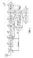
- FIG. 1 is a block diagram of an embodiment of a receiver unit capable of implementing various aspects and embodiments of the invention
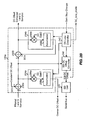
- FIG. 2B is a block diagram of an embodiment of a DC offset canceller
- FIG. 3 is a block diagram of an embodiment of a digital variable gain amplifier (DVGA);
- DVGA digital variable gain amplifier
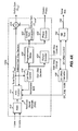
- FIG. 4A is a block diagram of an AGC loop unit
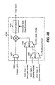
- FIG. 4B is a block diagram of an AGC control unit
- FIG. 4C is a diagram of an example gain transfer function for the RF/analog circuits.
- Direct downconverter 120 performs direct quadrature downconversion of the filtered RF signal from RF to baseband. This may be achieved by multiplying (or mixing) the filtered RF signal with a complex local oscillator (LO) signal to provide a complex baseband signal.
- the filtered RF signal may be mixed with an inphase LO signal to provide an inphase (I) baseband component and mixed with a quadrature LO signal to provide a quadrature (Q) baseband component.
- the mixer used to perform the direct downconversion may be implemented with multiple stages that may be controlled to provide different gains, as described below. In this case, the specific gain to be provided by the mixer may also be determined by another gain control message provided by SBI unit 150 via serial bus 152, as shown in FIG. 1 .
- the I and Q baseband components are then provided to one or more analog-to-digital converters (ADCs) 122.
- ADCs analog-to-digital converters
- ADCs 122 digitize the I and Q baseband components to provide I and Q samples, respectively.
- ADCs 122 may be implemented with various ADC designs, such as with sigma-delta modulators capable of filtering and then over-sampling the I and Q baseband components at multiple (e.g., 16) times the chip rate of the baseband components (which is 1.2288 Mcps for IS-95).
- the over-sampling allows the ADCs to provide a higher dynamic range and further allows the I and Q samples to be provided with fewer number of bits for a given precision.
- ADCs 122 provide 2-bit I and Q samples at 16 times the chip rate (i.e., chipx16). Other types of ADCs may also be used and are within the scope of the invention.
- the I and Q samples are provided from ADCs 122 to a digital filter 124.
- Digital filter 124 filters the I and Q samples to provide filtered I and Q samples, respectively.
- Digital filter 124 may perform any number of functions such as image rejection filtering, baseband pulse-matched filtering, decimation, sample rate conversion, and so on.
- digital filter 124 provides 18-bit filtered I and Q samples at chipx8 to a DC offset canceller 130.
- a controller 160 directs various operations of receiver unit 100. For example, controller 160 may direct the operation of the DC offset cancellation, the AGC loop, the DVGA, the SBI, and so on.
- a memory 162 provides storage for data and program codes for controller 160.
- FIG. 2A is a block diagram of a direct downconverter 120a, which is a specific embodiment of direct downconverter 120 in FIG. 1 .
- the filtered RF signal from receive filter 116 is provided to a mixer 212, which also receives a (complex) LO signal from a local oscillator 218.
- the frequency of the LO signal may be controlled by a frequency control signal (which may be provided via serial bus 152 or some other signal lines) and is set to the center frequency of the RF modulated signal being recovered.
- Mixer 212 then performs quadrature downconversion of the filtered RF signal with the complex LO signal to provide inphase and quadrature components, which are then provided to a summer 214.
- a converter 220 receives a digital DC offset control, which may be provided by DC offset canceller 130 via serial bus 152 and is denoted as SBI DC control in FIG. 2A .
- Converter 220 then performs digital-to-analog conversion of the digital control to generate DC offset control values of DC1I and DC1Q for the inphase and quadrature components, respectively. In an embodiment, these values are used to control the bias current of mixer 212 such that the DC offset in the signal components may be adjusted indirectly.
- Analog circuitry 222 receives an analog DC offset control, which may be provided by DC offset canceller 130 via a dedicated signal line and denoted as coarse DC offset in FIG. 2A . Analog circuitry 222 then performs filtering and possibly level shifting and scaling to generate DC offset values of DC2I and DC2Q for the inphase and quadrature components, respectively. Summer 214 then subtracts the DC offset values of DC2I and DC2Q from the inphase and quadrature components, respectively. The output components from summer 214 are then filtered and amplified by a lowpass filter/amplifier 216 to provide the I and Q baseband components.
- an analog DC offset control which may be provided by DC offset canceller 130 via a dedicated signal line and denoted as coarse DC offset in FIG. 2A . Analog circuitry 222 then performs filtering and possibly level shifting and scaling to generate DC offset values of DC2I and DC2Q for the inphase and quadrature components, respectively.
- Summer 214 subtracts the DC offset values of DC2I and DC2Q from
- Summer 214 within direct downconverter 120a and DC loop control unit 234a implement a coarse-grain DC loop that removes DC offset in the baseband components after the direct downconversion by mixer 212.
- Summer 232b and DC loop control unit 234b implement a fine-grain DC loop that removes DC offset that still remains after the coarse-grain DC loop. As their names imply, the fine-grain DC loop has higher resolution than the coarse-grain DC loop.
- SBI DC offset controller 240 periodically determines the SBI DC offset control based on various factors such as temperature, the gains of amplifier 114 and mixer 212, time, drift, and so on. The SBI DC offset control is then provided via serial bus 152 to converter 220, which then generates the corresponding DC offset control values of DC1I and DC1Q for mixer 212.
- Multiplier 316 multiplies the I or Q sample from AND gate 314 with a gain from a register 344 and provides the scaled (or amplified) sample to a truncation unit 318.
- multiplier 316 is operated at twice the sample rate, which is chipx16 for I/Q sample rate of chipx8.
- the input I and Q samples have 18 bits of resolution with 10 bits of resolution to the right of the binary point (i.e., 18Q10), the gain has 19 bits of resolution with 12 bits of resolution to the right of the binary point (i.e., 19Q12), and the scaled samples have 37 bits of resolution with 22 bits of resolution to the right of the binary point (i.e., 37Q22).
- Truncation unit 320 truncates the (e.g., 6) LSBs of each input sample and provides the truncated sample to the other input of multiplexer 322. Truncation unit 320 ensures that the output I and Q data have the same resolution regardless of whether the DVGA is enabled or bypassed.
- the AGC loop may also be designed to operate based on linear (instead of dB) gain values, and this is within the scope of the invention.
- the DC offset correction by the DC loop may be decoupled from the signal gain scaling by the DVGA.
- implementation of the DVGA in the digital domain after ADCs 122 further simplify the design of the RF/analog circuitry, which may lead to reduced cost for the direct downconversion receiver. Since the digital gain is provided after ADCs 122, the amplitude of the signal components provided to the ADCs could potentially be smaller, which would then require greater dynamic range for the analog-to-digital conversion process so that the ADC noise does not significantly degrade the SNR of the quantized I and Q samples.
- ADCs with high dynamic range may be provided by over-sampling sigma-delta modulators, as is known in the art.
- the AGC loop supports three loop modes - a normal mode, a low gain mode, and a freeze mode.
- the normal mode is used to provide a nominal AGC loop bandwidth
- the low gain mode is used to provide a smaller AGC loop bandwidth
- the freeze mode is used to freeze the AGC loop.
- the low gain and normal modes are associated with AGC loop gain values of AGC gain 1 and AGC gain 2, respectively.
- the freeze mode is achieved by zeroing out the value provided for accumulation by the AGC loop accumulator.
- an additional AGC loop gain value of AGC gain 3 is used for jammer detection.
- AGC gain 3 is typically smaller than AGC gain 2 for the normal mode but larger than AGC gain 1 for the low gain mode, and is used to detect for the presence of jammer in the signal components, as described below. Different or additional modes may also be supported by the AGC loop, and this is within the scope of the invention.
- the AGC gain 2 for the normal mode and the AGC gain 3 for jammer detection are provided to a multiplexer 446, which also receives the Nonbypass/hold control signal.
- the Nonbypass/hold control signal may be used to provide time hysteresis between gain steps (i.e., the AGC loop is maintained at a given gain step for a particular amount of time (Time 1 or Time 2) before it is allowed to switch to another (higher or lower) gain step.
- Multiplexer 446 then provides the AGC gain 2 when the normal mode is selected, which is indicated by the Nonbypass/hold control being set to logic low. Alternatively, multiplexer 446 provides the AGC gain 3 when jammer detection is to be performed, which is indicated by the Nonbypass/hold control being set to logic high.
- a multiplexer 448 receives the AGC gain 1 for the low gain mode and the output from multiplexer 448 at its two inputs and further receives the DC_loop_mode control signal. Multiplexer 448 then provides the AGC gain 1 to a multiplier 442 when the low gain mode is selected for the AGC loop when the DC loop is in the acquisition mode, which is indicated by the DC_loop_mode control being set to logic high. Alternatively, multiplexer 448 provides the AGC gain 2 or AGC gain 3 to multiplier 442 during the tracking mode, which is indicated by the DC_loop_mode control being set to logic low.
- An AND gate 440 receives the received signal strength estimate, RSS, and the Freeze_enb control. AND gate 440 then provides the RSS to multiplier 442 when (1) the DC loop is operated in the tracking mode or (2) the low gain mode is used for the AGC loop when the DC is operated in the acquisition mode. Alternatively, AND gate 440 provides a zero to multiplier 442 when the DC loop is operated in the acquisition mode and the AGC loop is frozen. The zero from AND gate 440 results in an accumulation of zero by AGC loop accumulator 444 when the AGC loop is frozen.
- accumulator 444 also receives the delayed gain step decision, which is indicative of the specific discrete gain to be used for the RF/analog circuits, as described below.
- Each discrete gain for the RF/analog circuits may be associated with a respective set of maximum and minimum values for the accumulation, which ensures stability in the AGC loop.
- the proper set of maximum and minimum values is used for the accumulation by accumulator 444.
- the coarse gain control for the RF/analog circuits is achieved by (1) mapping the total gain, G tatar , into a gain step decision by a gain step control unit 418, (2) encoding the gain step decision into the appropriate gain step controls by a range encoder 424, (3) formatting the gain step controls into the proper messages by SBI unit 150, (4) sending the messages to the RF/analog circuits (e.g., amplifier 114 and/or mixer 212) via serial bus 152, and (5) adjusting the gains of the RF/analog circuits based on the messages.
- the RF/analog circuits e.g., amplifier 114 and/or mixer 212
- the fine gain control is achieved by (1) determining the fine gain, G fine , for the DVGA by subtracting the coarse gain, G coarse , from the total gain, G total , and (2) adjusting the gain of the DVGA based on the fine gain.
- the derivation of the coarse and fine gains based on the total gain is described below.
- Receiver unit 100 may be designed with amplifier 114 having multiple (e.g., four) stages and mixer 212 having multiple (e.g., two) stages. Each stage may be associated with a specific discrete gain. Depending on which stages are turned ON/OFF, different discrete gains may be achieved. The coarse gain then controls the gains of the RF/analog circuits in coarse discrete steps. The specific discrete gain to be used for the RF/analog circuits is dependent on the received signal level, the specific designs of these circuits, and so on.
- FIG. 4C is a diagram of an example gain transfer function for the RF/analog circuits (e.g., amplifier 114 and mixer 212).
- the horizontal axis represents the total gain, which is inversely related to the received signal strength (i.e., higher gain corresponds to smaller received signal strength).
- the vertical axis represents the gain step decision provided by gain step control unit 418 based on the total gain. In this specific example design, the gain step decision takes on one of five possible values, which are defined in Table 1.
- hysteresis is provided in the transition between adjacent states. For example, while in the second state ("001"), the first LNA is not turned ON (to transition to the third state "010") until the total gain exceeds the L2 Rise threshold, and this LNA is not turned OFF (to transition from the second back to the first state) until the total gain falls below the L2 Fall threshold.
- the hysteresis (L2 Rise - L2 Fall) prevents the LNA from being continually turned OFF and ON if the total gain is between or near the L2 Rise and L2 Fall thresholds.
- Gain step control unit 418 determines the gain step decision based on the total gain, a transfer function such as the one shown in FIG. 4C (which is defined by the threshold values), and timing, jammer, and possibly other information.
- the gain step decision is indicative of the specific stages to be turned ON/OFF for amplifier 114 and mixer 212, as determined by the transfer function. Referring back to FIG. 4A , gain step control unit 418 then provides the gain step decision to programmable delay element 420 and range encoder 424.
- Range encoder 424 receives the gain step decision and provides the corresponding gain step control for each specific circuit to be controlled (e.g., one gain step control for amplifier 114 and another gain step control for mixer 212).
- the mapping between the gain step decision and gain step controls may be based on a look-up table and/or logic.
- Each gain step control comprises one or more bits and turns ON/OFF the designated stages within the circuit to be controlled by that gain step control.
- amplifier 114 may be designed with four stages, and its (2-bit) gain step control may be associated with four possible values ("00", “01”, “10”, and “11") for the four possible discrete gains for the amplifier.
- Mixer 212 may be designed with two stages, and its (1-bit) gain step control may be associated with two possible values ("0" and "1") for the two possible discrete gains for the mixer.
- the gain step controls for amplifier 114 and mixer 212 are formatted into the proper messages by SBI unit 150, and these messages are then sent to the circuits via serial bus 152.
- Range encoder 424 also provides to DC offset canceller 130 a gain step change signal that indicates whether or not the gain of the RF/analog circuitry has changed to a new value or step.
- the total gain, G total for the received signal may be decomposed into the coarse gain, G coarse , and the fine gain, G fine .
- the fine gain is generated by subtracting the coarse gain from the total gain by a summer 416. Since the coarse gain (in the form of the gain step controls) is provided to amplifier 114 and mixer 212 via SBI unit 150 and the serial bus, a delay is introduced between the time the coarse gain is determined by gain step control unit 418 and the time the coarse gain is actually applied by the RF/analog circuits. Moreover, processing delay is encountered by the received signal from the RF circuitry to the DVGA (e.g., especially digital filter 124).
- a programmable delay is used to delay the coarse gain (as indicated by the gain step decision) before it is applied to DVGA 140.
- Programmable delay element 420 provides a particular amount of delay for the gain step decision. This delay compensates for the delay introduced by SBI unit 150 and the delay of the received signal processing path from the RF circuitry to the DVGA. This delay may be programmed by writing a delay value to a register. Delay element 420 then provides the delayed gain step decision.
- a coarse gain conversion unit 422 receives the delayed gain step decision, which is indicative of a specific discrete gain for the RF/analog circuits, and provides the corresponding coarse gain, G coarse " having the proper range and resolution (e.g., the same range and resolution as for the total gain from AGC control unit 414).
- the coarse gain is thus equivalent to the gain step decision but is provided in a different format (i.e., the coarse gain is a high-resolution value whereas the gain step decision is a digital (ON/OFF) control).
- the gain step decision to coarse gain translation may be achieved with a look-up table and/or logic.
- the coarse gain is then subtracted from the total gain by summer 416 to provide the fine gain for the DVGA.
- phase rotation typically rotates by some particular step amount.
- the amount of phase rotation is dependent on which stages having been switched ON and OFF (as determined by the gain step decision) but is typically a fixed value for that particular setting or configuration. This phase rotation may result in degradation in the data demodulation process, until a frequency control loop is able to correct for the phase rotation.
- the gain step decision is mapped to a corresponding rotator phase, which is indicative of the amount of phase rotation in the received signal components due to the gain indicated by the gain step decision.
- the rotator phase is then provided to a rotator within digital demodulator 144 and used to adjust the phase of the I and Q data to account for the phase rotation introduced by the enabled gain stages in the RF/analog circuits.
- the mapping between gain step decision and rotator phase may be achieved with a look-up table and/or logic.
- fine resolution may be achieved for the rotator phase (e.g., 5.6° resolution may be achieved with 6 bits for the rotator phase)
- the DC loop operates on the filtered I and Q samples from digital filter 124 to remove DC offset, and the AGC loop (via DVGA 140) then operates on the DC offset corrected I and Q samples to provide the I and Q data that is then provided to digital demodulator 144.
- the AGC loop also controls the gain of the RF/analog circuitry, which in turn affects the amplitude of the I and Q samples operated on by the DC loop.
- the DC loop may thus be viewed as being embedded within the AGC loop. The operation of the DC loop affects the operation of the AGC loop.
- DC offset both static and time-varying
- Large DC offsets may be introduced in the signal components by various means.
- the gain of the RF/analog circuitry e.g., amplifier 114 and mixer 212
- large DC offsets may be introduced in the signal components due to mismatch in the different stages being switched ON/OFF.
- large DC offsets may also be introduced when the DC loop performs DC offset updates whereby different DC offset values of DC3I and DC3Q are provided to summer 232a and/or different DC offset values of DC1Q and DC1Q are provided to mixer 212 via the serial bus.
- Large DC offsets may be removed using various mechanisms of the DC loop (e.g., the coarse-grain and fine-grain loop DC loops). Moreover, large DC offsets may be more quickly removed by operating the DC loop in the acquisition mode. However, until they are removed, the large DC offsets have deleterious effects on the signal components and may degrade performance.
- any unremoved DC offset in the signal components appears as noise (whose power is equal to the DC offset) after the despreading operation by digital demodulator 144. This noise can degrade performance.
- a large DC offset disrupts the performance of the AGC loop in several ways.
- the DC offset adds to the signal components and results in combined (DC offset and signal) components having a larger amplitude.
- the reduced gain then causes compression of the desired signal components, with the amount of compression being proportional to the magnitude of the DC offset.
- the smaller amplitude for the desired signal components results in a degraded signal-to-quantization-noise ratio (SNR Q ), which also degrades performance.
- SNR Q signal-to-quantization-noise ratio
- a jammer may be generated by non-linearity in the circuits in the received signal path. Since non-linearity in amplifier 114 and mixer 212 are more pronounced when these circuits are operated at high gains (i.e., more stages being turned ON), the receiver may detect for jammers right after any of these circuits is switched to high gain. Jammer detection may be performed by measuring the power of the signal components with RSSI 412 right after the switch to a high gain, comparing the measured power against a threshold after a particular measurement time period, and declaring the presence of a jammer in the signal components if the measured power exceeds the threshold.
- the gain of one or more circuits may be reduced to either remove or mitigate the jammer.
- DC offset introduced by the switch to the high gain, it may not be possible to discern whether the increase in the measured power is due to jammer or to the total noise, which includes any unremoved DC offset and the increased DC loop noise generated by operating the DC loop in the acquisition mode to quickly remove the DC offset.
- the presence of DC offset may impact the ability to accurately detect for jammers, which may degrade performance if the RF/analog circuits are operated at the wrong gains due to erroneous detection of jammers.
- a large DC offset may cause long bursts of errors due to various deleterious effects described above.
- the degradation due to DC offset is more problematic at higher data rates since the time needed to remove DC spikes may be fixed (e.g., by the specific design of the DC loop), which then results in more errors at higher data rates.
- the duration of time the DC loop is operated in the acquisition mode is inversely proportional to the bandwidth of the DC loop in the acquisition mode.
- the DC loop bandwidth is designed to be wider in the acquisition mode to allow the DC loop to more quickly respond to and remove DC offset.
- Increasingly wider loop bandwidth corresponds to increasingly faster loop response.
- DC error in the desired signal components manifests as noise after the despreading operation within digital demodulator 144. This noise should be removed as quickly as possible, which may be achieved by increasing the bandwidth of the DC loop for the acquisition mode.
- the wider DC loop bandwidth also results in increased DC loop noise that may also degrade performance.
- the acquisition mode should trade off between the (introduced) DC offset to be corrected and the (self-generated) DC loop noise.
- the time duration in which the DC loop is operated in the acquisition mode may be set inversely proportional to the loop bandwidth.
- a wider DC loop bandwidth generally corresponds to a shorter DC offset acquisition time due to the wider loop's ability to more quickly respond.
- the shorter amount of time spent in the acquisition mode with the wider DC loop bandwidth takes advantage of this fact, and the DC loop is not operated in the acquisition mode for longer than necessary, which may then improve performance.
- the specific time duration to operate the DC loop in the acquisition mode may also be selected based on various other factors such as, for example, the expected amplitude of the DC offset, the amplitude of the DC loop noise, the modulation schemes, the bandwidth of the received signal, and so on.
- the acquisition mode duration is inversely related to the DC loop bandwidth in the acquisition mode, with the exact function being dependent on the factors noted above.
- the operation of the AGC loop is made dependent on the DC loop's operating mode.
- any un-removed DC offset which is typically larger when the DC loop changes into acquisition mode, affects the operation of the AGC loop.
- DC offset canceller 130 provides to AGC loop unit 142 the DC_loop_mode control signal, which indicates the DC loop's current operating mode.
- the AGC loop may simultaneously be switched to either the low gain mode or the freeze mode so that the AGC loop responds slowly or not at all to the DC offset while the DC loop is in the acquisition mode. The AGC loop may then be switched back to the normal mode after the DC loop transitions to the tracking mode.
- the small or zero AGC gain used while the DC loop is in the acquisition mode ensures that the AGC loop preserves its control signals during the DC acquisition period.
- the AGC control signals will then be ready to operate in the normal manner once the DC loop enters the tracking mode.
- the small or zero AGC gain also hinders or prevents the AGC loop from moving the power of the desired signal components from the AGC setpoint, and further reduces the impact of the DC offset in the jammer detection process, which would then reduce the likelihood of erroneous jammer detection.
- the specific normal and small AGC gains to be used may be determined by simulation, empirical measurement, or some other means. These gains may also be programmable (e.g., by controller 160).
- the controls for some or all of the RF/analog circuits are provided via serial bus 152.
- serial bus 152 The use of a standard serial bus to control RF/analog functions provides many advantages, as described below.
- the serial bus may be designed with various features to more effectively provide the required controls, as also described below.
- controls for RF/analog circuits are provided using dedicated signals between the circuits to be controlled and the controller providing the controls.
- One or more pins may be designated on the controller for each circuit to be individually controlled.
- three pins may be designated on the controller and the RF/analog chip to control the five stages of the amplifier/mixer described above.
- the use of designated pins for specific functions increases pin count and complicates board layout, which may lead to increased cost for the receiver.
- serial bus can be implemented with few pins (e.g., two or three) and these same pins can be used to provide control for multiple circuits implemented in one or more integrated circuits (ICs).
- ICs integrated circuits
- a single serial bus may be used to control the gain of amplifier 114, the gain of mixer 212, the DC offset of mixer 212, the frequency of oscillator 218, and so on.
- SBI unit 150 is designed to support a number of hardware request (HW_REQ) channels, each of which may be used to support a particular function. For example, one channel may be used for the VGA loop to set the step gains of amplifier 114 and mixer 212, and another channel may be used for the DC loop to set the DC offset control value (DC1) for mixer 212.
- HW_REQ hardware request
- the SBI unit may be designed to support any number of hardware request channels.
- Each circuit to be separately controlled may be associated with a respective address.
- Each message transmitted via the SBI unit includes the address of the circuit for which the message is transmitted.
- Each circuit coupled to the serial bus would then examine the address included in each transmitted message to determine whether or not the message is intended for that circuit, and would only process the message if it is addressed to that circuit.
- each hardware request channel may be designed with the ability to support a number of data transfer modes, which may include a fast transfer mode (FTM), an interrupt transfer mode (ITM), and a burst or bulk transfer mode (BTM).
- the fast transfer mode may be used to transmit multiple bytes to multiple circuits in accordance with the following the pattern: ID, ADDR, DATA, ADDR, DATA, ... where ID is the hardware request channel ID, ADDR is the address of the recipient circuit, and DATA is the data for the recipient circuit.
- the interrupt transfer mode may be used to transmit a single byte for broadcasting to one or more circuits coupled to the serial bus.
- burst transfer mode may be used to transmit multiple bytes to a specific circuit in accordance with the following the pattern: ID, ADDR, DATA1, DATA2, ....
- Different and/or additional transfer modes may also be implemented, and this is within the scope of the invention.
- the hardware request channels may be assigned specific priorities (e.g., by the controller).
- the priorities of the channels may be programmed into a register within SBI unit 150. The channels' priorities would then determine the order in which messages are sent, if multiple messages need to be sent by the SBI unit over the serial bus.
- a higher priority may be assigned to a channel used for a control loop requiring fast response (e.g., the gain step for amplifier 114 and mixer 212) and a lower priority may be assigned to a channel used for more static functions (e.g., the receive mode of direct downconverter 120, e.g., DFM and GPS).
- Each hardware request channel may also be associated with a respective enable flag that indicates whether or not that channel is enabled for use.
- the enable flags for all channels may be maintained by SBI unit 150.
- the serial bus comprises three signals - a data signal, a clock signal, and a strobe signal.
- the data signal is used to send the messages.
- the clock signal is provided by the sender (e.g., the controller) and used by the receivers to latch the data provided on the data signal.
- the strobe signal is used to indicate the start/stop of messages.
- Different serial bus designs with different signals and/or different number of signals may also be implemented, and this is within the scope of the invention.
- the various aspects and embodiments of the direct downconversion receiver described herein may be implemented in various wireless communication systems, such as CDMA systems, GPS systems, digital FM (DFM) systems, and so on.
- the direct downconversion receiver may also be used for the forward link or the reverse link in these communication systems.
- the various aspects and embodiments of the direct downconversion receiver described herein may be implemented by various means.
- all or some portions of the direct downconversion receiver may be implemented in hardware, software, or a combination thereof.
- the DVGA, DC offset correction, gain control, SBI, and so on may be implemented within one or more application specific integrated circuits (ASICs), digital signal processors (DSPs), digital signal processing devices (DSPDs), programmable logic devices (PLDs), field programmable gate arrays (FPGAs), processors, controllers, micro-controllers, microprocessors, other electronic units designed to perform the functions described herein, or a combination thereof.
- ASICs application specific integrated circuits
- DSPs digital signal processors
- DSPDs digital signal processing devices
- PLDs programmable logic devices
- FPGAs field programmable gate arrays
- processors controllers, micro-controllers, microprocessors, other electronic units designed to perform the functions described herein, or a combination thereof.
- the elements used for gain control and/or DC offset correction may be implemented with modules (e. g., procedures, functions, and so on) that perform the functions described herein.
- the software codes may be stored in a memory unit (e. g., memory 162 in FIG. 1 ) and executed by a processor (e. g., controller 160).
- the memory unit may be implemented within the processor or external to the processor, in which case it can be communicatively coupled to the processor via various means as is known in the art.
- an automatic gain control (AGC) apparatus comprising: an analog variable gain amplifier; a digital variable gain amplifier coupled to an output of the analog variable gain amplifier; and a gain controller adapted to measure a signal output from the digital variable gain amplifier and to control the gains of the analog and digital variable gain amplifiers.
- the apparatus may further comprise a DC offset canceller interposed between the output of the analog variable gain amplifier and an input of the digital variable gain amplifier, wherein an AGC loop gain is varied according to an operating mode of the DC offset canceller.
- an automatic gain control (AGC) loop in combination with a DC loop, comprising: selecting a particular DC operating mode for the DC loop from among a plurality of possible DC operating modes; operating the DC loop in the selected DC operating mode to correct for DC offset in a desired signal; selecting a particular AGC operating mode for the AGC loop from among a plurality of possible AGC operating modes based on the selected DC operating mode; and operating the AGC loop in the selected AGC operating mode to provide variable gain for the desired signal.
- AGC automatic gain control
- the plurality of possible DC operating modes may include an acquisition mode and a tracking mode.
- the acquisition mode may have a wider loop bandwidth than that of the tracking mode and is used to more quickly remove a large DC offset in the desired signal.
- Each of the plurality of possible AGC operating modes may be associated with a respective AGC loop gain.
- the plurality of possible AGC operating modes may include a normal mode and a low gain mode.
- the plurality of possible AGC operating modes may further include a freeze mode.
- the selected AGC operating mode may be a low gain mode when the selected DC operating mode is the acquisition mode.
- the selected AGC operating mode may be a freeze mode when the selected DC operating mode is the acquisition mode.
- a receiver unit in a wireless communication system comprising: a DC loop configurable to operate in one of a plurality of possible DC operating modes to correct for DC offset in a desired signal; and an automatic gain control (AGC) loop configurable to operate in one of a plurality of possible AGC operating modes to provide variable gain for the desired signal, wherein the particular AGC operating mode to be used is determined based on the particular DC operating mode selected for use for the DC loop.
- AGC automatic gain control
- an control apparatus in a wireless communication system, comprising: means for selecting a particular DC operating mode for a DC loop from among a plurality of possible DC operating modes; means for operating the DC loop in the selected DC operating mode to correct for DC offset in a desired signal; means for selecting a particular AGC operating mode for an automatic gain control (AGC) loop from among a plurality of possible AGC operating modes based on the selected DC operating mode; and means for operating the AGC loop in the selected AGC operating mode to 10 provide variable gain for the desired signal.
- AGC automatic gain control
- a method of operating a DC loop in a receiver unit comprising: selecting a particular operating mode for the DC loop from among a plurality of possible operating modes that include an acquisition mode; and if the selected operating mode is the acquisition mode, operating the DC loop in the acquisition mode for a particular time duration to correct for DC offset in a desired signal, wherein the particular time duration is inversely proportional to a loop bandwidth for the DC loop for the acquisition mode, and transitioning out of the acquisition mode after the particular time duration.
- the acquisition mode may be selected in response to an event expected to result in a large DC offset in the desired signal.
- the event may correspond to a switch to new analog circuit stages to process the desired signal.
- the event may correspond to application of a new DC offset value to correct for static DC offset in the desired signal.
- the plurality of possible operating modes may further include a tracking mode.
- the transition may be made from the acquisition mode to the tracking mode after the particular time duration.
- the particular time duration may be further selected based on an expected amplitude of the DC offset in the desired signal.
- the particular time duration may be further selected to minimize a combination of DC offset introduced in the desired signal and loop noise from the DC loop.
- a DC loop in a receiver unit comprising: a summer operative to subtract a DC offset value from a desired signal to provide a DC offset corrected signal; and a loop control unit configurable to operate in one of a plurality of possible operating modes to provide the DC offset value, wherein the plurality of possible operating modes include an acquisition mode having a particular loop bandwidth, and wherein the loop control unit is operated in the acquisition mode, when selected, for a particular time duration inversely proportional to the loop bandwidth for the acquisition mode and to transition out of the acquisition mode after the particular time duration.
- an apparatus in a receiver unit comprising: means for selecting a particular operating mode for a DC loop from among a plurality of possible operating modes that include an acquisition mode; and means for operating the DC loop in the acquisition mode for a particular time duration, if the selected operating mode is the acquisition mode, to correct for DC offset in a desired signal, wherein the particular time duration is inversely proportional to a loop bandwidth for the DC loop for the acquisition mode, and means for transitioning out of the acquisition mode after the particular time duration.
- a method of digitally amplifying a desired signal comprising: receiving a gain represented in a logarithm format; determining a difference between the received gain and a gain offset; converting the difference, represented in the logarithm format, to an output gain represented in a linear format; and digitally multiplying the desired signal with the output gain.
- a digital variable gain amplifier comprising: a first unit operative to receive a gain represented in a logarithm format and to determine a difference between the received gain and a gain offset; a second unit operative to convert the difference, represented in the logarithm format, to an output gain represented in a linear format ; and a digital multiplier operative to multiply input samples with the output gain to provide output data.
- DVGA digital variable gain amplifier
- the DVGA may further comprise a multiplexer operative to multiplex inphase and quadrature input samples into a single sequence of samples, and wherein the digital multiplier is operative to multiply the inphase and quadrature input samples in a time-division multiplexed manner.
- an apparatus for digitally amplifying a desired signal comprising: means for receiving a gain represented in a logarithm format ; means for determining a difference between the received gain and a gain offset; means for converting the difference, represented in the logarithm format, to an output gain represented in a linear format; and means for digitally multiplying the desired signal with the output gain.
- a method of controlling one or more analog circuits via a serial bus comprising: receiving a control for a particular analog circuit; forming a message corresponding to the received control; sending the message over the serial bus; receiving the message at the particular analog circuit; and adjusting one or more characteristics of the particular analog circuit based on the received message.
- the particular analog circuit may be an amplifier configurable to operate at one of a plurality of discrete gains, and wherein the message is indicative of a specific discrete gain to be used for the amplifier.
- the message may be used to adjust a bias current for the particular analog circuit.
- the message may be used to adjust the frequency for a signal generated by the particular analog circuit.
- Each of the one or more analog circuits may be assigned a respective priority, and wherein messages are sent to the one or more analog circuits based in part on their assigned priorities.
- Each of the one or more analog circuits is associated with a respective address.
- an apparatus for controlling one or more analog circuits via a serial bus comprising: means for receiving a control for a particular analog circuit; means for forming a message corresponding to the received control; means for sending the message over the serial bus; means for receiving the message at the particular analog circuit; and means for adjusting one or more characteristics of the particular analog circuit based on the received message.
- a receiver unit comprising: an RF front-end unit operative to amplify, downconvert, and digitize a received signal to provide samples; a digital signal processor operative to process the samples to provide output data; and a serial bus interface (SBI) unit operative to provide controls for the RF frontend unit via a serial bus.
- SBI serial bus interface
- the SBI unit may be configured to support a plurality of hardware request channels. Each hardware request channel may be associated with a respective priority. Each hardware request channel may be operable to send messages via a plurality of possible data transfer modes. The plurality of possible data transfer modes may include a fast transfer mode and an interrupt transfer mode.
- a method of processing a desired signal in a wireless communication system comprising: amplifying the desired signal with a first gain having a coarse resolution; downconverting the amplified signal from radio frequency (RF) to baseband with a single frequency downconversion stage; digitizing the downconverted signal to provide samples; and digitally amplifying the samples with a second gain having a fine resolution to provide output data having a desired signal amplitude.
- RF radio frequency
- the method may further comprise: correcting for DC offset in the samples with a DC loop, wherein the DC offset corrected samples are digitally amplified.
- a direct downconversion receiver comprising: an RF front-end unit operative to amplify, downconvert, and digitize a received signal to provide samples; a digital variable gain amplifier (DVGA) operative to amplify the samples with a first gain to provide output data having a desired signal amplitude; and an automatic gain control (AGC) loop operative to provide the first gain for the DVGA based in part on the output data.
- RF front-end unit operative to amplify, downconvert, and digitize a received signal to provide samples
- DVGA digital variable gain amplifier
- AGC automatic gain control
- the direct downconversion receiver may further comprise: a DC offset canceller operative to correct for DC offset in the samples, and wherein the DVGA is operative to amplify the DC offset corrected samples.
- the AGC loop may be further operative to provide a second gain for the RF front-end unit.
- an apparatus in a wireless communication system comprising: first means for amplifying a received signal; means for canceling a DC offset in the amplified signal; second means for digitally amplifying the DC offset cancelled signal; and means for measuring the digitally amplified signal and to control the gains of the first and second amplifying means.
- a receiver unit comprising: an analog variable gain amplifier; a DC offset canceller coupled to an output of the analog variable gain amplifier; a digital variable gain amplifier coupled to an output of the DC offset canceller; a gain controller adapted to measure a signal output from the digital variable gain amplifier and to control the gains of the analog and digital variable gain amplifiers; and a serial bus interface (SBI) unit operative to provide the gain for the analog variable gain amplifier via a serial bus.
- SBI serial bus interface
- a receiver unit comprising: an RF front-end unit operative to amplify, downconvert, and digitize a received signal to provide samples; a DC loop operative to cancel DC offset in the samples; a digital variable gain amplifier (DVGA) operative to amplify the DC offset canceled samples with a first gain to provide output data having a desired signal amplitude; an automatic gain control (AGC) loop operative to provide the first gain for the DVGA and a second gain for the RF front-end unit based in part on the output data; and a serial bus interface (SBI) unit operative to provide the second gain to the RF front-end unit.
- AGC automatic gain control
- SBI serial bus interface
Landscapes
- Engineering & Computer Science (AREA)
- Computer Networks & Wireless Communication (AREA)
- Signal Processing (AREA)
- Circuits Of Receivers In General (AREA)
- Control Of Amplification And Gain Control (AREA)
- Digital Transmission Methods That Use Modulated Carrier Waves (AREA)
- Amplifiers (AREA)
- Information Transfer Systems (AREA)
- Selective Calling Equipment (AREA)
- Communication Control (AREA)
- Noise Elimination (AREA)
Applications Claiming Priority (3)
| Application Number | Priority Date | Filing Date | Title |
|---|---|---|---|
| US26962301P | 2001-02-16 | 2001-02-16 | |
| US10/034,734 US7076225B2 (en) | 2001-02-16 | 2001-12-21 | Variable gain selection in direct conversion receiver |
| EP02709570A EP1402631B1 (de) | 2001-02-16 | 2002-02-15 | Homodynempfänger |
Related Parent Applications (1)
| Application Number | Title | Priority Date | Filing Date |
|---|---|---|---|
| EP02709570.2 Division | 2002-02-15 |
Publications (2)
| Publication Number | Publication Date |
|---|---|
| EP2267889A2 true EP2267889A2 (de) | 2010-12-29 |
| EP2267889A3 EP2267889A3 (de) | 2012-08-01 |
Family
ID=26711303
Family Applications (7)
| Application Number | Title | Priority Date | Filing Date |
|---|---|---|---|
| EP10177172A Withdrawn EP2267888A3 (de) | 2001-02-16 | 2002-02-15 | Direktumwandlungs-Empfängerarchitektur |
| EP20100177214 Withdrawn EP2273674A3 (de) | 2001-02-16 | 2002-02-15 | Direktumwandlungs-Empfängerarchitektur |
| EP10177192A Withdrawn EP2267890A3 (de) | 2001-02-16 | 2002-02-15 | Direktumwandlungs-Empfängerarchitektur |
| EP02709570A Expired - Lifetime EP1402631B1 (de) | 2001-02-16 | 2002-02-15 | Homodynempfänger |
| EP10177163A Withdrawn EP2267887A3 (de) | 2001-02-16 | 2002-02-15 | Direktumwandlungs-Empfängerarchitektur |
| EP10177198.8A Expired - Lifetime EP2267891B1 (de) | 2001-02-16 | 2002-02-15 | Direktumwandlungs-Empfängerarchitektur |
| EP10177184A Withdrawn EP2267889A3 (de) | 2001-02-16 | 2002-02-15 | Direktumwandlungs-Empfängerarchitektur |
Family Applications Before (6)
| Application Number | Title | Priority Date | Filing Date |
|---|---|---|---|
| EP10177172A Withdrawn EP2267888A3 (de) | 2001-02-16 | 2002-02-15 | Direktumwandlungs-Empfängerarchitektur |
| EP20100177214 Withdrawn EP2273674A3 (de) | 2001-02-16 | 2002-02-15 | Direktumwandlungs-Empfängerarchitektur |
| EP10177192A Withdrawn EP2267890A3 (de) | 2001-02-16 | 2002-02-15 | Direktumwandlungs-Empfängerarchitektur |
| EP02709570A Expired - Lifetime EP1402631B1 (de) | 2001-02-16 | 2002-02-15 | Homodynempfänger |
| EP10177163A Withdrawn EP2267887A3 (de) | 2001-02-16 | 2002-02-15 | Direktumwandlungs-Empfängerarchitektur |
| EP10177198.8A Expired - Lifetime EP2267891B1 (de) | 2001-02-16 | 2002-02-15 | Direktumwandlungs-Empfängerarchitektur |
Country Status (12)
| Country | Link |
|---|---|
| US (5) | US7076225B2 (de) |
| EP (7) | EP2267888A3 (de) |
| JP (6) | JP2005507568A (de) |
| KR (6) | KR100913037B1 (de) |
| CN (3) | CN100411302C (de) |
| AT (1) | ATE510351T1 (de) |
| AU (4) | AU2002244049B8 (de) |
| BR (1) | BRPI0207274B1 (de) |
| CA (3) | CA2723046C (de) |
| MX (1) | MXPA03007359A (de) |
| RU (3) | RU2379825C2 (de) |
| WO (1) | WO2002067420A2 (de) |
Families Citing this family (180)
| Publication number | Priority date | Publication date | Assignee | Title |
|---|---|---|---|---|
| US7076225B2 (en) * | 2001-02-16 | 2006-07-11 | Qualcomm Incorporated | Variable gain selection in direct conversion receiver |
| EP1296449B1 (de) * | 2001-09-25 | 2007-10-31 | Sony Deutschland GmbH | Automatische Verstärkungsregelung |
| EP1306978B1 (de) * | 2001-10-26 | 2005-05-25 | STMicroelectronics N.V. | Direktmischempfänger für einem Kommunikationssystem mit nicht konstanter Hüllkurve |
| US6907089B2 (en) * | 2001-11-14 | 2005-06-14 | Broadcom, Corp. | Digital demodulation and applications thereof |
| US20050164659A1 (en) * | 2001-11-27 | 2005-07-28 | Infineon Technologies Ag | Apparatus and method for correcting sudden phase changes in received signals in mobile stations |
| JP3852919B2 (ja) | 2001-12-25 | 2006-12-06 | 株式会社東芝 | 無線受信機 |
| US6819910B2 (en) * | 2002-03-08 | 2004-11-16 | Broadcom Corp. | Radio employing a self calibrating transmitter with reuse of receiver circuitry |
| US7024169B2 (en) | 2002-01-25 | 2006-04-04 | Qualcomm Incorporated | AMPS receiver using a zero-IF architecture |
| JP3805258B2 (ja) * | 2002-01-29 | 2006-08-02 | 松下電器産業株式会社 | ダイレクトコンバージョン受信機 |
| US7657241B2 (en) * | 2002-02-01 | 2010-02-02 | Qualcomm, Incorporated | Distortion reduction calibration |
| US6985711B2 (en) * | 2002-04-09 | 2006-01-10 | Qualcomm, Incorporated | Direct current offset cancellation for mobile station modems using direct conversion |
| US7212797B2 (en) * | 2002-04-26 | 2007-05-01 | Qualcomm Incorporated | DC removal techniques for wireless networking |
| KR100474085B1 (ko) * | 2003-02-07 | 2005-03-10 | 인티그런트 테크놀로지즈(주) | 디씨 오프셋 보상 회로 및 방법과 이를 이용한 신호 처리장치 |
| JP4195000B2 (ja) * | 2002-05-23 | 2008-12-10 | アンテルユニヴェルシテール・ミクロ−エレクトロニカ・サントリュム・ヴェー・ゼッド・ドゥブルヴェ | Iqの不均衡を推定して補償するための方法及び装置 |
| JP2004015409A (ja) * | 2002-06-06 | 2004-01-15 | Renesas Technology Corp | 通信用半導体集積回路および無線通信システム |
| US8559559B2 (en) * | 2002-06-20 | 2013-10-15 | Qualcomm, Incorporated | Method and apparatus for compensating DC offsets in communication systems |
| JP2004048581A (ja) * | 2002-07-15 | 2004-02-12 | Hitachi Ltd | 受信装置及び利得制御システム |
| KR100517971B1 (ko) * | 2002-09-07 | 2005-09-30 | 엘지전자 주식회사 | 이동통신 시스템의 고정점 결정장치 및 방법 |
| US6999537B2 (en) | 2002-10-25 | 2006-02-14 | Qualcomm Incorporated | Method of removing DC offset for a ZIF-based GSM radio solution with digital frequency correlation |
| EP1801985A3 (de) * | 2002-10-25 | 2007-07-18 | Qualcomm, Incorporated | Verfahren zur Beseitigung des Gleichanteil-Offsets in einem Direktkonversionsempfänger mit digitaler Frequenz-Offset-Beseitigung |
| US7430406B2 (en) * | 2002-11-08 | 2008-09-30 | Qualcomm Incorporated | Gain control in a wireless device |
| US20040097209A1 (en) * | 2002-11-14 | 2004-05-20 | Haub David R. | Automatic gain control apparatus and methods |
| EP1620955A1 (de) * | 2002-11-18 | 2006-02-01 | Koninklijke Philips Electronics N.V. | Automatische verstärkungsregelung die signal und störleistung verwenden |
| US8144810B2 (en) * | 2003-02-19 | 2012-03-27 | Csr Technology Inc. | Serial radio frequency to baseband interface with programmable clock |
| US8903348B2 (en) * | 2003-02-19 | 2014-12-02 | Csr Technology Inc. | Serial radio frequency to baseband interface with power control |
| JP4222368B2 (ja) * | 2003-02-20 | 2009-02-12 | 日本電気株式会社 | 信号処理装置、及びダイレクトコンバージョン受信装置 |
| US7203459B2 (en) * | 2003-04-03 | 2007-04-10 | Pctel, Inc. | Mode adaptation in wireless systems |
| JP3906179B2 (ja) * | 2003-04-25 | 2007-04-18 | 株式会社東芝 | 無線受信機および無線信号処理方法 |
| US7280812B2 (en) * | 2003-06-06 | 2007-10-09 | Interdigital Technology Corporation | Digital baseband receiver with DC discharge and gain control circuits |
| US7215722B2 (en) * | 2003-06-09 | 2007-05-08 | Ali Corporation | Device for WLAN baseband processing with DC offset reduction |
| US7277688B2 (en) * | 2003-06-17 | 2007-10-02 | Broadcom Corporation | DC offset correction for very low intermediate frequency receiver |
| US7359692B2 (en) * | 2003-06-30 | 2008-04-15 | Zarbana Digital Fund, Llc | Method of and device for antennae diversity switching |
| US7227916B2 (en) * | 2003-08-26 | 2007-06-05 | Freescale Semiconductor, Inc. | Receiver with automatic gain control that operates with multiple protocols and method thereof |
| KR101015716B1 (ko) * | 2003-10-27 | 2011-02-22 | 삼성전자주식회사 | 이동통신 시스템에서 이동 단말의 수신 장치 및 신호 수신방법 |
| US7454184B2 (en) * | 2003-12-02 | 2008-11-18 | Skyworks Solutions, Inc. | DC offset cancellation in a wireless receiver |
| US7522892B2 (en) * | 2003-12-22 | 2009-04-21 | Black Sand Technologies, Inc. | Power amplifier with serial interface and associated methods |
| US7502601B2 (en) * | 2003-12-22 | 2009-03-10 | Black Sand Technologies, Inc. | Power amplifier with digital power control and associated methods |
| US7203476B2 (en) * | 2004-01-09 | 2007-04-10 | Motorola, Inc. | Method and apparatus for minimizing baseband offset error in a receiver |
| US7409189B2 (en) * | 2004-03-30 | 2008-08-05 | Intel Corporation | Calibration and testing architecture for receivers |
| CN101002385B (zh) * | 2004-04-09 | 2010-10-06 | 上海奇普科技有限公司 | 控制均衡器的前馈滤波器的装置和方法 |
| CA2562563A1 (en) * | 2004-04-13 | 2005-10-27 | Maxlinear, Inc. | Method and apparatus for dc offset removal |
| US7773702B2 (en) | 2004-05-03 | 2010-08-10 | Qualcomm Incorporated | Gain control for a receiver in a multi-carrier communication system |
| US7570696B2 (en) * | 2004-06-25 | 2009-08-04 | Intel Corporation | Multiple input multiple output multicarrier communication system and methods with quantized beamforming feedback |
| US20080298518A1 (en) * | 2004-08-12 | 2008-12-04 | Gopalan Krishnamurthy | Automatic Gain Control Unit of a Receiver |
| US7415264B2 (en) * | 2004-09-25 | 2008-08-19 | Skyworks Solutions, Inc. | Low noise filter for a wireless receiver |
| KR100663476B1 (ko) * | 2004-10-11 | 2007-01-02 | 삼성전자주식회사 | 통신 시스템의 무선 단말기에서 송수신 장치의 이득을 제어하기 위한 장치 및 방법 |
| CA2583654C (en) * | 2004-10-12 | 2015-02-17 | Maxlinear, Inc. | A receiver architecture with digitally generated intermediate frequency |
| CA2583657A1 (en) * | 2004-10-12 | 2006-04-27 | Maxlinear, Inc. | A hybrid receiver architecture using upconversion followed by direct downconversion |
| EP1648093B1 (de) * | 2004-10-15 | 2011-08-03 | Broadcom Corporation | Unterdrücker einer unerwünschten Harmoniewelle in einem RF-Bandtaktgenerator |
| US7593707B2 (en) * | 2004-11-01 | 2009-09-22 | Broadcom Corp. | Method and system for compensation of DC offset in an RF receiver |
| KR100737944B1 (ko) * | 2004-11-11 | 2007-07-13 | 인티그런트 테크놀로지즈(주) | 디지털 멀티미디어 방송용 직접 변환 수신기 |
| US7313376B1 (en) * | 2004-11-12 | 2007-12-25 | Rf Micro Devices, Inc. | DC offset correction for a wireless communication system |
| US7228120B2 (en) * | 2004-11-18 | 2007-06-05 | Freescale Semiconductor, Inc. | Circuit and method for reducing direct current biases |
| DE102004057766B4 (de) * | 2004-11-30 | 2007-06-21 | Advanced Micro Devices, Inc., Sunnyvale | Funkschnittstellensteuerung auf Grundlage einer Ereignislistenspezifikation |
| CN100382439C (zh) * | 2004-12-02 | 2008-04-16 | 大唐移动通信设备有限公司 | 直接变频收信机的自干扰信号消除方法 |
| US8340616B2 (en) * | 2004-12-16 | 2012-12-25 | Entropic Communications, Inc. | Tracking filter for tuner |
| US7353010B1 (en) * | 2004-12-22 | 2008-04-01 | Atheros Communications, Inc. | Techniques for fast automatic gain control |
| US20060193410A1 (en) * | 2005-02-28 | 2006-08-31 | Moorti R T | Gain estimation for multiple receiver systems |
| WO2006099083A1 (en) * | 2005-03-10 | 2006-09-21 | Qualcomm Incorporated | A method to track analog gain step magnitudes online during operation of wireless mobile devices |
| US20060227910A1 (en) * | 2005-03-11 | 2006-10-12 | Nangavalli Ramasubramanian | Receiver DC offset correction |
| US7496341B2 (en) * | 2005-03-24 | 2009-02-24 | Integrated System Solution Corp. | Device and method for providing DC-offset estimation |
| FR2884987B1 (fr) * | 2005-04-26 | 2007-08-17 | Eads Telecom Soc Par Actions S | Reglage du gain d'une chaine de reception radio |
| US7515929B2 (en) * | 2005-04-27 | 2009-04-07 | Skyworks Solutions, Inc. | Receiver for a multimode radio |
| US7505744B1 (en) * | 2005-07-28 | 2009-03-17 | Rf Micro Devices, Inc. | DC offset correction using multiple configurable feedback loops |
| KR100654466B1 (ko) * | 2005-09-26 | 2006-12-06 | 삼성전자주식회사 | 바이어스 전류를 제어하는 rf 신호 수신 장치 및바이어스 전류 제어 방법 |
| US20070087711A1 (en) * | 2005-10-19 | 2007-04-19 | Broadcom Corporation | Multiple band transceiver |
| US7636386B2 (en) * | 2005-11-15 | 2009-12-22 | Panasonic Corporation | Method of continuously calibrating the gain for a multi-path angle modulator |
| KR101125948B1 (ko) * | 2005-12-28 | 2012-03-21 | 엘지전자 주식회사 | 다단계의 가변이득을 갖는 저잡음 증폭장치 및 그 방법 |
| US7889820B2 (en) * | 2006-01-05 | 2011-02-15 | Qualcomm Incorporated | Phase compensation for analog gain switching in OFDM modulated physical channel |
| US7835467B2 (en) * | 2006-01-05 | 2010-11-16 | Qualcomm, Incorporated | DC offset correction for high gain complex filter |
| DE102006005032B4 (de) * | 2006-02-03 | 2018-06-28 | Intel Deutschland Gmbh | Empfangsverfahren mit digitaler Pegeleinstellung im Analogteil und stufenweiser Pegelveränderung im Digitalteil |
| US7539471B2 (en) * | 2006-03-30 | 2009-05-26 | Intel Corporation | Method and apparatus to provide variable gain in a radio receiver front end |
| JP2007281633A (ja) * | 2006-04-04 | 2007-10-25 | Niigata Seimitsu Kk | 受信機 |
| US7701371B2 (en) * | 2006-04-04 | 2010-04-20 | Qualcomm Incorporated | Digital gain computation for automatic gain control |
| US7515578B2 (en) * | 2006-05-08 | 2009-04-07 | Skyhook Wireless, Inc. | Estimation of position using WLAN access point radio propagation characteristics in a WLAN positioning system |
| US7551579B2 (en) | 2006-05-08 | 2009-06-23 | Skyhook Wireless, Inc. | Calculation of quality of wlan access point characterization for use in a wlan positioning system |
| US8781426B2 (en) * | 2006-05-15 | 2014-07-15 | Qualcomm Incorporated | Techniques for controlling operation of control loops in a receiver |
| JP4973029B2 (ja) * | 2006-06-30 | 2012-07-11 | 富士通株式会社 | 受信装置及びその利得制御方法 |
| US8144673B2 (en) | 2006-07-07 | 2012-03-27 | Skyhook Wireless, Inc. | Method and system for employing a dedicated device for position estimation by a WLAN positioning system |
| US8295371B2 (en) * | 2006-07-14 | 2012-10-23 | Qualcomm Incorporated | Multi-carrier receiver for wireless communication |
| EP1881646B1 (de) * | 2006-07-20 | 2009-04-01 | Telefonaktiebolaget LM Ericsson (publ) | Funkempfänger |
| US7656327B2 (en) * | 2006-07-24 | 2010-02-02 | Qualcomm, Incorporated | Saturation detection for analog-to-digital converter |
| KR100803032B1 (ko) * | 2006-10-19 | 2008-02-18 | 지씨티 세미컨덕터 인코포레이티드 | 과도 신호를 보상하기 위한 수신기, 디지털 신호 처리부 및 디지털 신호 처리 방법 |
| US7856234B2 (en) * | 2006-11-07 | 2010-12-21 | Skyhook Wireless, Inc. | System and method for estimating positioning error within a WLAN-based positioning system |
| US7873125B2 (en) * | 2006-11-30 | 2011-01-18 | Broadcom Corporation | Method and system for sliding window phase estimator for WCDMA automatic frequency correction |
| US7912437B2 (en) * | 2007-01-09 | 2011-03-22 | Freescale Semiconductor, Inc. | Radio frequency receiver having dynamic bandwidth control and method of operation |
| US8144811B2 (en) * | 2007-01-26 | 2012-03-27 | Qualcomm Atheros, Inc. | Hybrid zero-IF receiver |
| JP4556960B2 (ja) * | 2007-02-27 | 2010-10-06 | セイコーエプソン株式会社 | アナログフロントエンド回路及び電子機器 |
| US9083940B2 (en) * | 2007-03-14 | 2015-07-14 | Steve Selby | Automatic gain control system |
| US8112050B2 (en) * | 2007-03-14 | 2012-02-07 | Texas Instruments Incorporated | Reducing power consumption in receivers employing conversion to intermediate frequency |
| EP2140640A1 (de) * | 2007-03-19 | 2010-01-06 | ACN Advanced Communications Networks SA | Verfahren zur robusten synchronisation eines mehrträgerempfängers unter verwendung von filterbanken und entsprechender empfänger und sender/empfänger |
| CN101720296B (zh) * | 2007-05-30 | 2012-08-22 | 施奥泰尔有限公司 | 舵桨驱动器及舵桨驱动方法 |
| US8185682B2 (en) * | 2007-06-01 | 2012-05-22 | International Business Machines Corporation | USB 2.0 bi-directional bus channel with boost circuitry |
| US20090040107A1 (en) * | 2007-06-12 | 2009-02-12 | Hmicro, Inc. | Smart antenna subsystem |
| US20090042527A1 (en) * | 2007-06-12 | 2009-02-12 | Hmicro Inc. | Dynamic low power receiver |
| US7659779B2 (en) * | 2007-07-31 | 2010-02-09 | Broadcom Corporation | Method and system for polar modulating OFDM signals with discontinuous phase |
| US7602242B2 (en) * | 2007-07-31 | 2009-10-13 | Broadcom Corporation | Method and system for polar modulating QAM signals with discontinuous phase |
| US7551026B2 (en) * | 2007-07-31 | 2009-06-23 | Broadcom Corporation | Method and system for polar modulation with discontinuous phase for RF transmitters with power control |
| US7982539B2 (en) * | 2007-08-22 | 2011-07-19 | Nanoamp Mobile, Inc. | High resolution variable gain control |
| US20090058531A1 (en) * | 2007-08-31 | 2009-03-05 | Nanoamp Solutions Inc. (Cayman) | Variable gain amplifier |
| JP2009088972A (ja) * | 2007-09-28 | 2009-04-23 | Toshiba Corp | 無線通信の受信装置 |
| US7692486B2 (en) * | 2007-10-05 | 2010-04-06 | Qualcomm, Incorporated | Configurable feedback for an amplifier |
| EP2210352B1 (de) * | 2007-10-24 | 2020-05-06 | LifeSignals, Inc. | Systeme und netze für drahtlose halb- und vollduplexkommunikation unter verwendung mehrerer funkgeräte |
| US8626079B2 (en) * | 2007-12-12 | 2014-01-07 | Electronics And Telecommunications Research Institute | Link adaptation method and apparatus in wireless communication system |
| US8218684B2 (en) * | 2008-01-15 | 2012-07-10 | Broadcom Corporation | Method and system for an adaptive automatic gain control (AGC) reference for HSDPA and WCDMA |
| FR2926421B1 (fr) * | 2008-01-15 | 2009-12-18 | Commissariat Energie Atomique | Systeme d'emission radiofrequence |
| WO2009100401A2 (en) | 2008-02-06 | 2009-08-13 | Hmicro, Inc. | Wireless communications systems using multiple radios |
| US8213555B2 (en) * | 2008-03-05 | 2012-07-03 | Texas Instruments Incorporated | Methods and apparatus to improve distortion performance and direct current (DC) offset cancellation in receivers |
| US8259876B2 (en) * | 2008-03-21 | 2012-09-04 | Skyworks Solutions, Inc. | System and method for tuning a radio receiver |
| US8331892B2 (en) * | 2008-03-29 | 2012-12-11 | Qualcomm Incorporated | Method and system for DC compensation and AGC |
| US7760122B1 (en) * | 2008-05-02 | 2010-07-20 | Pmc-Sierra, Inc. | Power optimized ADC for wireless transceivers |
| US8086199B2 (en) * | 2008-05-22 | 2011-12-27 | Cisco Technology, Inc. | Sharing AGC loop between demodulator and spectrum analysis system |
| US8260227B2 (en) * | 2008-06-10 | 2012-09-04 | Mediatek Inc. | Direct conversion receiver and DC offset concellation method |
| US8334805B2 (en) * | 2008-07-15 | 2012-12-18 | Qualcomm Incorporated | Digital front end for a satellite navigation receiver |
| TWI385916B (zh) * | 2008-07-18 | 2013-02-11 | Airoha Tech Corp | 無線接收器之增益控制電路 |
| WO2010023597A1 (en) * | 2008-09-01 | 2010-03-04 | Nxp B.V. | Frequency hopping receiver circuit |
| US8666343B2 (en) * | 2008-09-15 | 2014-03-04 | Analog Devices, Inc. | DC-offset-correction system and method for communication receivers |
| EP2184851B1 (de) | 2008-11-07 | 2016-10-05 | Telefonaktiebolaget LM Ericsson (publ) | Verfahren und Vorrichtung zum Regeln der Verstärkung eines Radioempfängers |
| US8126094B2 (en) * | 2009-01-07 | 2012-02-28 | Skyworks Solutions, Inc. | Circuits, systems, and methods for managing automatic gain control in quadrature signal paths of a receiver |
| US7982992B2 (en) * | 2009-01-09 | 2011-07-19 | International Business Machines Corporation | Dual gain control for magnetic data storage system |
| US8130021B2 (en) | 2009-01-09 | 2012-03-06 | International Business Machines Corporation | Gain control with multiple integrators |
| EP2267892A1 (de) * | 2009-06-19 | 2010-12-29 | Thomson Licensing | Empfänger mit analoger und digitaler Verstärkungsregelung und entsprechendes Verfahren |
| KR101259576B1 (ko) | 2009-06-25 | 2013-04-30 | 창원대학교 산학협력단 | Bps 수신장치 |
| US20110021207A1 (en) * | 2009-07-24 | 2011-01-27 | Morgan Edward J | System and Method for Estimating Positioning Error Within a WLAN-Based Positioning System |
| CN102045101B (zh) * | 2009-10-10 | 2014-05-07 | 博通集成电路(上海)有限公司 | 用于星形网络中工作在突发模式下的帧接收机及方法 |
| JP2011166773A (ja) * | 2010-02-11 | 2011-08-25 | Korea Electronics Telecommun | サブサンプリング技法を利用する受信器のデジタル処理構造 |
| US8634766B2 (en) | 2010-02-16 | 2014-01-21 | Andrew Llc | Gain measurement and monitoring for wireless communication systems |
| JP5686983B2 (ja) * | 2010-03-30 | 2015-03-18 | ジーイー・メディカル・システムズ・グローバル・テクノロジー・カンパニー・エルエルシー | 信号処理装置および磁気共鳴イメージング装置 |
| GB201005764D0 (en) * | 2010-04-07 | 2010-05-26 | Icera Inc | Gain adjuster |
| US8284817B2 (en) | 2010-06-30 | 2012-10-09 | Qualcomm Atheros, Inc. | Measuring received signal strength on neighboring frequencies of a channel with interference in a wireless device |
| CN102347781B (zh) * | 2010-08-03 | 2014-04-30 | 鸿富锦精密工业(深圳)有限公司 | 无线收发设备 |
| US9124467B2 (en) | 2010-11-30 | 2015-09-01 | Telefonaktiebolaget L M Ericsson (Publ) | Receiver gain adjustment to reducing an influence of a DC offset |
| JP5599352B2 (ja) * | 2011-03-30 | 2014-10-01 | パナソニック株式会社 | 受信装置 |
| WO2011100920A2 (zh) | 2011-04-13 | 2011-08-25 | 华为技术有限公司 | 无线接收机中自动增益调整的方法及装置 |
| WO2012147138A1 (ja) * | 2011-04-26 | 2012-11-01 | パナソニック株式会社 | 受信機 |
| US8983418B2 (en) * | 2011-06-20 | 2015-03-17 | Broadcom Corporation | Multi-stage gain control in receivers and other circuits |
| WO2012176139A1 (en) * | 2011-06-22 | 2012-12-27 | Renesas Mobile Corporation | Method, apparatus and computer program for setting a radio frequency gain |
| CN103703683B (zh) * | 2011-07-08 | 2016-03-16 | 日本电气株式会社 | 接收装置以及增益控制方法 |
| ITBO20110453A1 (it) * | 2011-07-28 | 2011-10-27 | Marposs Spa | Sistema per controllare posizione e/o dimensioni di pezzi meccanici |
| KR101184861B1 (ko) * | 2011-09-27 | 2012-09-20 | 한국전력공사 | 전력량계의 직류 오프셋 제거장치 및 방법 |
| RU2498501C2 (ru) * | 2011-12-29 | 2013-11-10 | Федеральное государственное бюджетное образовательное учреждение высшего профессионального образования "Волгоградский государственный университет" | Способ уменьшения погрешностей усилителя постоянного тока с модулятором на входе и демодулятором на выходе |
| US9275690B2 (en) | 2012-05-30 | 2016-03-01 | Tahoe Rf Semiconductor, Inc. | Power management in an electronic system through reducing energy usage of a battery and/or controlling an output power of an amplifier thereof |
| US9509351B2 (en) | 2012-07-27 | 2016-11-29 | Tahoe Rf Semiconductor, Inc. | Simultaneous accommodation of a low power signal and an interfering signal in a radio frequency (RF) receiver |
| US9094079B2 (en) | 2012-10-08 | 2015-07-28 | Qualcomm Incorporated | System and method for I-Q imbalance correction |
| US8768277B1 (en) * | 2012-12-19 | 2014-07-01 | Em Microelectronics-Marin S.A. | Automatic gain control of a receiver circuit |
| US9037104B2 (en) | 2013-02-04 | 2015-05-19 | Qualcomm, Incorporated | Receiver that reconfigures between zero intermediate frequency and direct sampling based on channel conditions |
| US9837714B2 (en) | 2013-03-15 | 2017-12-05 | Integrated Device Technology, Inc. | Extending beamforming capability of a coupled voltage controlled oscillator (VCO) array during local oscillator (LO) signal generation through a circular configuration thereof |
| US9722310B2 (en) | 2013-03-15 | 2017-08-01 | Gigpeak, Inc. | Extending beamforming capability of a coupled voltage controlled oscillator (VCO) array during local oscillator (LO) signal generation through frequency multiplication |
| US9666942B2 (en) | 2013-03-15 | 2017-05-30 | Gigpeak, Inc. | Adaptive transmit array for beam-steering |
| US9184498B2 (en) | 2013-03-15 | 2015-11-10 | Gigoptix, Inc. | Extending beamforming capability of a coupled voltage controlled oscillator (VCO) array during local oscillator (LO) signal generation through fine control of a tunable frequency of a tank circuit of a VCO thereof |
| US9716315B2 (en) | 2013-03-15 | 2017-07-25 | Gigpeak, Inc. | Automatic high-resolution adaptive beam-steering |
| US9531070B2 (en) | 2013-03-15 | 2016-12-27 | Christopher T. Schiller | Extending beamforming capability of a coupled voltage controlled oscillator (VCO) array during local oscillator (LO) signal generation through accommodating differential coupling between VCOs thereof |
| US9780449B2 (en) | 2013-03-15 | 2017-10-03 | Integrated Device Technology, Inc. | Phase shift based improved reference input frequency signal injection into a coupled voltage controlled oscillator (VCO) array during local oscillator (LO) signal generation to reduce a phase-steering requirement during beamforming |
| US9425842B2 (en) * | 2014-05-30 | 2016-08-23 | Peraso Technologies Inc. | Method, system and apparatus for automatic gain control in direct-conversion receiver |
| US9391578B2 (en) * | 2014-06-11 | 2016-07-12 | Analog Devices Global | Low intermediate frequency receiver |
| CN104601186B (zh) * | 2014-11-19 | 2017-05-17 | 深圳市中兴微电子技术有限公司 | 一种直流失配消除方法和装置 |
| US10079647B2 (en) | 2014-12-10 | 2018-09-18 | Nxp Usa, Inc. | DC offset calibration of wireless receivers |
| DE102015104809B4 (de) * | 2015-03-27 | 2026-05-07 | Apple Inc. | Eine Vorrichtung und ein Verfahren zum Verarbeiten eines Signals, das von einem empfangenen Radiofrequenzsignal abhängt |
| US9608587B2 (en) | 2015-06-25 | 2017-03-28 | Freescale Semiconductor, Inc. | Systems and methods to dynamically calibrate and adjust gains in a direct conversion receiver |
| TWI575890B (zh) * | 2015-10-19 | 2017-03-21 | 瑞昱半導體股份有限公司 | 通訊接收端及其自動增益控制方法 |
| US10145937B2 (en) * | 2016-04-01 | 2018-12-04 | Texas Instruments Incorporated | Dynamic IQ mismatch correction in FMCW radar |
| WO2019107264A1 (ja) | 2017-12-01 | 2019-06-06 | 株式会社村田製作所 | 増幅装置、増幅装置の製造方法およびバイアス電流補正方法 |
| CN108123693B (zh) * | 2017-12-20 | 2021-06-15 | 湖南智领通信科技有限公司 | 一种提高射频功率放大器效率的自动控制方法 |
| JP2021513286A (ja) * | 2018-02-08 | 2021-05-20 | ビーエーイー・システムズ・オーストラリア・リミテッド | アナログ・デジタルコンバータのための改良された自動利得制御 |
| EP3672092B1 (de) * | 2018-12-19 | 2022-01-26 | Nxp B.V. | Verfahren und system zur verstärkungsregelung in einer kommunikationsvorrichtung |
| JP7056611B2 (ja) * | 2019-02-27 | 2022-04-19 | 株式会社Jvcケンウッド | 受信装置、プログラム |
| TWI703813B (zh) * | 2019-04-23 | 2020-09-01 | 瑞昱半導體股份有限公司 | 訊號補償裝置 |
| US12206365B2 (en) | 2021-06-18 | 2025-01-21 | Qorvo Us, Inc. | Voltage ripple suppression in a transmission circuit |
| US12199577B2 (en) | 2021-06-18 | 2025-01-14 | Qorvo Us, Inc. | Envelope tracking voltage correction in a transmission circuit |
| US12284003B2 (en) | 2021-09-16 | 2025-04-22 | Qorvo Us, Inc. | Phase and amplitude error correction in a transmission circuit |
| US12323174B2 (en) | 2021-09-16 | 2025-06-03 | Qorvo Us, Inc. | Amplitude-to-phase error correction in a transceiver circuit |
| US12401332B2 (en) | 2021-09-16 | 2025-08-26 | Qorvo Us, Inc. | Phase and amplitude error correction in a transmission circuit |
| CN114204949B (zh) * | 2021-11-30 | 2024-01-30 | 西南电子技术研究所(中国电子科技集团公司第十研究所) | 大动态快速数字agc控制方法 |
| US12526001B2 (en) | 2022-01-18 | 2026-01-13 | Qorvo Us, Inc. | Linearized front-end operation using information from baseband circuit |
| US12273081B2 (en) | 2022-01-27 | 2025-04-08 | Qorvo Us, Inc. | Voltage ripple reduction in a power management circuit |
| US12549138B1 (en) | 2022-04-12 | 2026-02-10 | Qorvo Us, Inc. | Bandwidth adaptation in a transmission circuit |
| US12489402B2 (en) | 2022-05-31 | 2025-12-02 | Qorvo Us, Inc. | Voltage ripple reduction in a power management circuit |
| US12381525B2 (en) * | 2022-06-28 | 2025-08-05 | Qorvo Us, Inc. | Amplifier system |
| US11909405B1 (en) * | 2023-01-09 | 2024-02-20 | Infineon Technologies Ag | Digital coarse locking in digital phase-locked loops |
| US12456957B2 (en) | 2023-01-20 | 2025-10-28 | Qorvo Us, Inc. | Amplitude and phase error correction in a wireless communication circuit |
Citations (5)
| Publication number | Priority date | Publication date | Assignee | Title |
|---|---|---|---|---|
| EP0785632A2 (de) * | 1996-01-19 | 1997-07-23 | Sharp Kabushiki Kaisha | Spread-Spektrum-Empfänger |
| US5764689A (en) * | 1995-12-06 | 1998-06-09 | Rockwell International Corporation | Variable digital automatic gain control in a cordless direct sequence spread spectrum telephone |
| US5901347A (en) * | 1996-01-17 | 1999-05-04 | Motorola, Inc. | Fast automatic gain control circuit and method for zero intermediate frequency receivers and radiotelephone using same |
| US6038435A (en) * | 1997-12-24 | 2000-03-14 | Nortel Networks Corporation | Variable step-size AGC |
| WO2000031867A1 (en) * | 1998-11-24 | 2000-06-02 | Telefonaktiebolaget Lm Ericsson (Publ) | Automatic gain control for slotted mode operation |
Family Cites Families (151)
| Publication number | Priority date | Publication date | Assignee | Title |
|---|---|---|---|---|
| US656447A (en) * | 1897-10-18 | 1900-08-21 | John Martin | Band-cutter and feeder. |
| SU489200A1 (ru) * | 1972-06-23 | 1975-10-25 | Ленинградский Электротехнический Институт Связи Им.Профессора Бонч-Бруевича | Устройство автоматической регулировки усилени |
| US4025869A (en) | 1976-04-12 | 1977-05-24 | Beckman Instruments, Inc. | Solid state amplifier |
| US4213097A (en) * | 1978-10-19 | 1980-07-15 | Racal-Milgo, Inc. | Hybrid automatic gain control circuit |
| NL191374C (nl) * | 1980-04-23 | 1995-06-16 | Philips Nv | Communicatiesysteem met een communicatiebus. |
| JPS5799010A (en) * | 1980-12-11 | 1982-06-19 | Fujitsu Ltd | High dynamic range digital agc system |
| GB2166324A (en) * | 1984-10-25 | 1986-04-30 | Stc Plc | A multi-mode radio transceiver |
| US4731796A (en) | 1984-10-25 | 1988-03-15 | Stc, Plc | Multi-mode radio transceiver |
| JPS61169030A (ja) * | 1985-01-22 | 1986-07-30 | Nec Corp | 受信回路 |
| JPS63260208A (ja) * | 1987-04-17 | 1988-10-27 | Kenwood Corp | デジタルagc方式 |
| US5093807A (en) * | 1987-12-23 | 1992-03-03 | Texas Instruments Incorporated | Video frame storage system |
| US4870370A (en) | 1988-02-19 | 1989-09-26 | Silicon Systems, Inc. | Method and apparatus for two stage automatic gain control |
| JPH01307343A (ja) | 1988-06-06 | 1989-12-12 | Mitsubishi Electric Corp | ディジタル復調装置 |
| US4989074A (en) * | 1988-09-27 | 1991-01-29 | Matsushita Electric Industrial Co., Ltd. | Digital automatic gain control apparatus |
| JPH0714217B2 (ja) * | 1988-09-27 | 1995-02-15 | 松下電器産業株式会社 | 自動利得制御装置 |
| IE62843B1 (en) * | 1989-03-16 | 1995-03-08 | Taldat Ltd | Automatic gain control devices |
| US5014013A (en) * | 1989-10-06 | 1991-05-07 | Hewlett-Packart Company | Antilog circuit with automatic gain control |
| US5263194A (en) | 1990-03-07 | 1993-11-16 | Seiko Corp. | Zero if radio receiver for intermittent operation |
| JP2973451B2 (ja) * | 1990-03-08 | 1999-11-08 | ソニー株式会社 | 利得制御回路 |
| US5095533A (en) | 1990-03-23 | 1992-03-10 | Rockwell International Corporation | Automatic gain control system for a direct conversion receiver |
| US5179730A (en) | 1990-03-23 | 1993-01-12 | Rockwell International Corporation | Selectivity system for a direct conversion receiver |
| JPH0437397A (ja) * | 1990-06-01 | 1992-02-07 | Pioneer Electron Corp | 遠隔制御システム |
| JPH0434099U (de) * | 1990-07-13 | 1992-03-19 | ||
| JPH04101516A (ja) * | 1990-08-21 | 1992-04-03 | Casio Comput Co Ltd | A/d変換器のオフセット補償回路 |
| US5146504A (en) * | 1990-12-07 | 1992-09-08 | Motorola, Inc. | Speech selective automatic gain control |
| US5163164A (en) * | 1990-12-31 | 1992-11-10 | Thomson Consumer Electronics, Inc. | Microprocessor controlled digital aft unit |
| JPH04255101A (ja) * | 1991-01-30 | 1992-09-10 | Sanyo Electric Co Ltd | 自動利得制御回路 |
| US5212827A (en) | 1991-02-04 | 1993-05-18 | Motorola, Inc. | Zero intermediate frequency noise blanker |
| US5379075A (en) * | 1992-02-04 | 1995-01-03 | Sony Corporation | Video signal AGC circuit for adjusting the sync level of a video signal |
| KR950701472A (ko) * | 1992-06-08 | 1995-03-23 | 다니엘 케이. 니콜스 | 자동 이득 제어 회로 및 수신기(Receiver automatic gain control) |
| US5341249A (en) * | 1992-08-27 | 1994-08-23 | Quantum Corporation | Disk drive using PRML class IV sampling data detection with digital adaptive equalization |
| EP0594894B1 (de) | 1992-10-28 | 1999-03-31 | Alcatel | Offsetgleichspannungskorrektur für Direktmisch-TDMA-Empfänger |
| JPH08147237A (ja) * | 1993-03-05 | 1996-06-07 | Toshiba Corp | バス・ア−ビトレ−ション方式 |
| US5504785A (en) * | 1993-05-28 | 1996-04-02 | Tv/Com Technologies, Inc. | Digital receiver for variable symbol rate communications |
| EP0701745B1 (de) * | 1993-06-04 | 1999-09-15 | Rca Thomson Licensing Corporation | Tuner mit direktumsetzung |
| GB2286950B (en) * | 1994-02-22 | 1998-06-17 | Roke Manor Research | A direct conversion receiver |
| US5451948A (en) * | 1994-02-28 | 1995-09-19 | Cubic Communications, Inc. | Apparatus and method for combining analog and digital automatic gain control in receivers with digital signal processing |
| US5463662A (en) * | 1994-04-08 | 1995-10-31 | Echelon Corporation | Apparatus and method for reducing errors in data caused by noise through use of blanking |
| US5469115A (en) | 1994-04-28 | 1995-11-21 | Qualcomm Incorporated | Method and apparatus for automatic gain control in a digital receiver |
| ZA95605B (en) * | 1994-04-28 | 1995-12-20 | Qualcomm Inc | Method and apparatus for automatic gain control and dc offset cancellation in quadrature receiver |
| US5459679A (en) * | 1994-07-18 | 1995-10-17 | Quantum Corporation | Real-time DC offset control and associated method |
| JPH0846987A (ja) * | 1994-07-27 | 1996-02-16 | Sony Corp | Acc回路 |
| US5835785A (en) * | 1994-11-14 | 1998-11-10 | Motorola, Inc. | Multiplexed three line synchronous/full-duplex asychronous data bus and method therefor |
| ZA9510509B (en) * | 1994-12-23 | 1996-05-30 | Qualcomm Inc | Dual-mode digital FM communication system |
| JPH08316997A (ja) * | 1995-05-15 | 1996-11-29 | Matsushita Electric Ind Co Ltd | 受信装置 |
| US5629960A (en) * | 1995-05-22 | 1997-05-13 | Sierra Wireless, Inc. | Method for reducing distortion effects on DC off-set voltage and symbol clock tracking in a demodulator |
| JPH08340268A (ja) * | 1995-06-13 | 1996-12-24 | Matsushita Electric Ind Co Ltd | 受信機 |
| JP4091671B2 (ja) * | 1995-08-08 | 2008-05-28 | 松下電器産業株式会社 | 直流オフセット補償装置 |
| JP3425277B2 (ja) * | 1995-08-25 | 2003-07-14 | 株式会社東芝 | 無線受信機 |
| US5627857A (en) * | 1995-09-15 | 1997-05-06 | Qualcomm Incorporated | Linearized digital automatic gain control |
| JPH09130245A (ja) * | 1995-11-06 | 1997-05-16 | Sony Corp | ゲイン可変回路 |
| US5881376A (en) * | 1995-12-15 | 1999-03-09 | Telefonaktiebolaget Lm Ericsson | Digital calibration of a transceiver |
| FI106328B (fi) * | 1996-02-08 | 2001-01-15 | Nokia Mobile Phones Ltd | Menetelmä ja piirijärjestely vastaanotetun signaalin käsittelemiseksi |
| JPH09224059A (ja) | 1996-02-15 | 1997-08-26 | General Res Of Electron Inc | 直接変換fsk受信機 |
| US5758274A (en) * | 1996-03-13 | 1998-05-26 | Symbol Technologies, Inc. | Radio frequency receiver with automatic gain control |
| JPH09321559A (ja) | 1996-05-24 | 1997-12-12 | Oki Electric Ind Co Ltd | 自動利得制御回路 |
| US6028537A (en) | 1996-06-14 | 2000-02-22 | Prince Corporation | Vehicle communication and remote control system |
| US6498929B1 (en) | 1996-06-21 | 2002-12-24 | Kabushiki Kaisha Toshiba | Receiver having DC offset decreasing function and communication system using the same |
| JP3575952B2 (ja) * | 1996-06-21 | 2004-10-13 | 株式会社東芝 | 直流オフセット除去機能を備えた受信機およびこれを用いた通信システム |
| US5898912A (en) | 1996-07-01 | 1999-04-27 | Motorola, Inc. | Direct current (DC) offset compensation method and apparatus |
| JPH1041992A (ja) * | 1996-07-24 | 1998-02-13 | Nippon Telegr & Teleph Corp <Ntt> | 準同期検波復調装置 |
| JP3178707B2 (ja) * | 1996-08-23 | 2001-06-25 | 株式会社バーテックススタンダード | Agc方式 |
| JP3120737B2 (ja) * | 1996-08-23 | 2000-12-25 | 日本電気株式会社 | 自動利得制御回路 |
| US5705949A (en) * | 1996-09-13 | 1998-01-06 | U.S. Robotics Access Corp. | Compensation method for I/Q channel imbalance errors |
| US6018553A (en) | 1996-09-18 | 2000-01-25 | Wireless Access | Multi-level mixer architecture for direct conversion of FSK signals |
| US6275543B1 (en) | 1996-10-11 | 2001-08-14 | Arraycomm, Inc. | Method for reference signal generation in the presence of frequency offsets in a communications station with spatial processing |
| US5742899A (en) | 1996-10-24 | 1998-04-21 | Motorola, Inc. | Fast attack automatic gain control (AGC) loop for narrow band receivers |
| TW377533B (en) * | 1996-11-06 | 1999-12-21 | Koninkl Philips Electronics Nv | Radio receiver for receiving a main radio broadcast signal and a monolithic integrated circuit for use in such radio receiver |
| JP3468264B2 (ja) | 1996-12-09 | 2003-11-17 | ソニー株式会社 | オフセット補償回路および方法 |
| US5917865A (en) * | 1996-12-31 | 1999-06-29 | Lucent Technologies, Inc. | Digital automatic gain control employing two-stage gain-determination process |
| JP3468009B2 (ja) * | 1997-02-19 | 2003-11-17 | 三菱電機株式会社 | 受信機 |
| JP3731276B2 (ja) * | 1997-03-03 | 2006-01-05 | 三菱電機株式会社 | 受信機 |
| US6175728B1 (en) * | 1997-03-05 | 2001-01-16 | Nec Corporation | Direct conversion receiver capable of canceling DC offset voltages |
| KR100244274B1 (ko) | 1997-04-15 | 2000-02-01 | 김영환 | 디램(DRAM) 오버드라이브 센싱(Overdrive Sensing) 기구 |
| JP3413060B2 (ja) * | 1997-05-13 | 2003-06-03 | 松下電器産業株式会社 | 直接変換受信機 |
| US6006079A (en) | 1997-06-13 | 1999-12-21 | Motorola, Inc. | Radio having a fast adapting direct conversion receiver |
| US6029052A (en) | 1997-07-01 | 2000-02-22 | Telefonaktiebolaget Lm Ericsson | Multiple-mode direct conversion receiver |
| WO1999004487A1 (en) * | 1997-07-18 | 1999-01-28 | Koninklijke Philips Electronics N.V. | Signal-processing device |
| JPH1139851A (ja) * | 1997-07-22 | 1999-02-12 | Clarion Co Ltd | オーディオユニット選択装置 |
| US6240100B1 (en) | 1997-07-31 | 2001-05-29 | Motorola, Inc. | Cellular TDMA base station receiver with dynamic DC offset correction |
| US6025965A (en) * | 1997-08-29 | 2000-02-15 | Quantum Corporation | Control loops for low power, high speed PRML sampling data detection channel |
| US6043787A (en) * | 1997-09-19 | 2000-03-28 | Endgate Corporation | Beam modifying trough waveguide antenna |
| JPH11110344A (ja) * | 1997-09-29 | 1999-04-23 | Ricoh Co Ltd | バス調停装置 |
| US6005506A (en) * | 1997-12-09 | 1999-12-21 | Qualcomm, Incorporated | Receiver with sigma-delta analog-to-digital converter for sampling a received signal |
| US6175279B1 (en) * | 1997-12-09 | 2001-01-16 | Qualcomm Incorporated | Amplifier with adjustable bias current |
| US6219741B1 (en) * | 1997-12-10 | 2001-04-17 | Intel Corporation | Transactions supporting interrupt destination redirection and level triggered interrupt semantics |
| AU2274899A (en) * | 1997-12-18 | 1999-07-12 | Sony International (Europe) Gmbh | N-port direct receiver |
| JP3328926B2 (ja) * | 1998-02-26 | 2002-09-30 | 船井電機株式会社 | テレビジョン受信装置 |
| US6516187B1 (en) * | 1998-03-13 | 2003-02-04 | Maxim Integrated Products, Inc. | DC offset correction for direct conversion tuner IC |
| JP3349948B2 (ja) * | 1998-03-23 | 2002-11-25 | 沖電気工業株式会社 | アナログ/ディジタル変換装置 |
| JPH11284677A (ja) | 1998-03-27 | 1999-10-15 | Nec Corp | 復調器とこれを用いたディジタル無線通信システム |
| US6108558A (en) * | 1998-04-21 | 2000-08-22 | Motorola, Inc. | Method for calculating a location of a remote Unit utilizing observed time difference (OTD) and real time difference (RTD) measurements. |
| US6192225B1 (en) * | 1998-04-22 | 2001-02-20 | Ericsson Inc. | Direct conversion receiver |
| JPH11331300A (ja) * | 1998-05-19 | 1999-11-30 | Nec Corp | 復調装置 |
| US6205183B1 (en) | 1998-05-29 | 2001-03-20 | Ericsson Inc. | Methods of suppressing reference oscillator harmonic interference and related receivers |
| JP3576410B2 (ja) * | 1998-05-29 | 2004-10-13 | 松下電器産業株式会社 | 受信装置と送受信装置及び方法 |
| AU4843299A (en) * | 1998-07-01 | 2000-01-24 | Qualcomm Incorporated | Improved inter-device serial bus protocol |
| US6243569B1 (en) | 1998-08-12 | 2001-06-05 | Analog Devices, Inc. | Direct conversion circuit for radio frequency signals |
| US7065327B1 (en) | 1998-09-10 | 2006-06-20 | Intel Corporation | Single-chip CMOS direct-conversion transceiver |
| WO2000019621A1 (fr) | 1998-09-30 | 2000-04-06 | Mitsubishi Denki Kabushiki Kaisha | Recepteur a conversion directe d'harmonique paire, et emetteur-recepteur comprenant ce recepteur |
| US6160859A (en) * | 1998-10-19 | 2000-12-12 | Motorola, Inc. | Integrated multi-mode bandpass sigma-delta receiver subsystem with interference mitigation and method of using the same |
| US6560301B1 (en) | 1998-10-21 | 2003-05-06 | Parkervision, Inc. | Integrated frequency translation and selectivity with a variety of filter embodiments |
| FI106660B (fi) | 1998-11-06 | 2001-03-15 | Nokia Mobile Phones Ltd | Menetelmä ja järjestely radiovastaanottimen linearisoimiseksi |
| JP3022530B1 (ja) | 1998-12-07 | 2000-03-21 | 日本電気株式会社 | Cdma無線通信システムにおけるマルチキャスト通信方式 |
| US6366622B1 (en) | 1998-12-18 | 2002-04-02 | Silicon Wave, Inc. | Apparatus and method for wireless communications |
| US6304751B1 (en) * | 1998-12-29 | 2001-10-16 | Cirrus Logic, Inc. | Circuits, systems and methods for digital correction of phase and magnitude errors in image reject mixers |
| US6798789B1 (en) * | 1999-01-27 | 2004-09-28 | Motorola, Inc. | Priority enhanced messaging and method therefor |
| CN1192495C (zh) | 1999-02-24 | 2005-03-09 | 三菱电机株式会社 | 无线终端装置 |
| JP2000252868A (ja) * | 1999-03-01 | 2000-09-14 | Toshiba Corp | Cdma通信装置とその自動利得制御回路 |
| JP2000295053A (ja) * | 1999-04-01 | 2000-10-20 | New Japan Radio Co Ltd | Tvチューナ回路 |
| JP2000295304A (ja) | 1999-04-02 | 2000-10-20 | Nec Corp | 復調装置 |
| US6167242A (en) * | 1999-04-23 | 2000-12-26 | Linear Technology Corporation | Offset voltage cancellation system for radio frequency power controllers |
| DE60001960T2 (de) | 1999-05-24 | 2003-11-13 | Level One Communications, Inc. | Automatische verstärkungsregelung und offsetkorrektur |
| US6535560B1 (en) | 1999-06-03 | 2003-03-18 | Ditrans Corporation | Coherent adaptive calibration system and method |
| US6516183B1 (en) | 1999-09-10 | 2003-02-04 | Telefonaktiebolaget Lm Ericsson (Publ) | Method and apparatus for disturbance compensation of a direct conversion receiver in a full duplex transceiver |
| US6556635B1 (en) | 1999-11-09 | 2003-04-29 | Lsi Logic Corporation | Communications receiver having adaptive dynamic range |
| NO329890B1 (no) | 1999-11-15 | 2011-01-17 | Hitachi Ltd | Mobilkommunikasjonsapparat |
| US6557062B1 (en) * | 1999-12-09 | 2003-04-29 | Trw Inc. | System and method for low-noise control of radio frequency devices |
| KR20010057146A (ko) | 1999-12-18 | 2001-07-04 | 윤종용 | 자동이득제어기능을 구비한 직접 변환 복조장치 |
| US6442380B1 (en) * | 1999-12-22 | 2002-08-27 | U.S. Philips Corporation | Automatic gain control in a zero intermediate frequency radio device |
| US6327313B1 (en) * | 1999-12-29 | 2001-12-04 | Motorola, Inc. | Method and apparatus for DC offset correction |
| US6321073B1 (en) * | 2000-01-31 | 2001-11-20 | Motorola, Inc. | Radiotelephone receiver and method with improved dynamic range and DC offset correction |
| US6459889B1 (en) * | 2000-02-29 | 2002-10-01 | Motorola, Inc. | DC offset correction loop for radio receiver |
| US6771945B1 (en) | 2000-05-24 | 2004-08-03 | General Dynamics Decision Systems, Inc. | Dynamic DC balancing of a direct conversion receiver and method |
| US6654594B1 (en) | 2000-05-30 | 2003-11-25 | Motorola, Inc. | Digitized automatic gain control system and methods for a controlled gain receiver |
| FI114591B (fi) | 2000-05-30 | 2004-11-15 | Nokia Corp | Menetelmä lähetin/vastaanottimen toteuttamiseksi sekä lähetin/vastaanotin |
| US6668164B2 (en) * | 2000-06-01 | 2003-12-23 | Motorola, Inc. | Method and apparatus for reducing intermodulation distortion in a low current drain automatic gain control system |
| JP2001358791A (ja) * | 2000-06-15 | 2001-12-26 | Mitsubishi Electric Corp | 自動利得制御回路 |
| JP3489621B2 (ja) | 2000-09-28 | 2004-01-26 | 日本電気株式会社 | ダイレクトコンバージョン受信機のベースバンド回路 |
| US6748200B1 (en) * | 2000-10-02 | 2004-06-08 | Mark A. Webster | Automatic gain control system and method for a ZIF architecture |
| US7068987B2 (en) * | 2000-10-02 | 2006-06-27 | Conexant, Inc. | Packet acquisition and channel tracking for a wireless communication device configured in a zero intermediate frequency architecture |
| US6947720B2 (en) | 2000-10-17 | 2005-09-20 | Rf Micro Devices, Inc. | Low noise mixer circuit with improved gain |
| US6654593B1 (en) | 2000-10-30 | 2003-11-25 | Research In Motion Limited | Combined discrete automatic gain control (AGC) and DC estimation |
| AU2002246874A1 (en) * | 2001-01-02 | 2002-08-06 | Intersil Americas Inc. | Precision automatic gain control circuit |
| US6509777B2 (en) | 2001-01-23 | 2003-01-21 | Resonext Communications, Inc. | Method and apparatus for reducing DC offset |
| US6606489B2 (en) | 2001-02-14 | 2003-08-12 | Rf Micro Devices, Inc. | Differential to single-ended converter with large output swing |
| US7076225B2 (en) | 2001-02-16 | 2006-07-11 | Qualcomm Incorporated | Variable gain selection in direct conversion receiver |
| US6560447B2 (en) * | 2001-03-05 | 2003-05-06 | Motorola, Inc. | DC offset correction scheme for wireless receivers |
| US6766153B2 (en) | 2001-04-02 | 2004-07-20 | Itran Communications Ltd. | Dynamic automatic gain control circuit employing kalman filtering |
| US6732228B1 (en) * | 2001-07-19 | 2004-05-04 | Network Elements, Inc. | Multi-protocol data classification using on-chip CAM |
| US7231000B2 (en) | 2001-10-22 | 2007-06-12 | Broadcom Corporation | System and method for DC offset compensation and bit synchronization |
| US7072427B2 (en) | 2001-11-09 | 2006-07-04 | Parkervision, Inc. | Method and apparatus for reducing DC offsets in a communication system |
| US6775530B2 (en) * | 2001-11-27 | 2004-08-10 | Qualcomm Inc. | Direct conversion of narrow-band RF signals |
| US6700514B2 (en) | 2002-03-14 | 2004-03-02 | Nec Corporation | Feed-forward DC-offset canceller for direct conversion receiver |
| US6985711B2 (en) | 2002-04-09 | 2006-01-10 | Qualcomm, Incorporated | Direct current offset cancellation for mobile station modems using direct conversion |
| US6836647B2 (en) | 2002-04-10 | 2004-12-28 | Nokia Corporation | Device and method for CDMA-signal power estimation |
| US7212797B2 (en) | 2002-04-26 | 2007-05-01 | Qualcomm Incorporated | DC removal techniques for wireless networking |
| JP2004048581A (ja) | 2002-07-15 | 2004-02-12 | Hitachi Ltd | 受信装置及び利得制御システム |
| US7085334B2 (en) | 2002-09-30 | 2006-08-01 | Lsi Logic Corporation | Automatic gain control with analog and digital gain |
| JP2005284710A (ja) | 2004-03-30 | 2005-10-13 | Sanyo Electric Co Ltd | 駆動回路 |
| US7098732B2 (en) | 2004-09-30 | 2006-08-29 | Silicon Laboratories Inc. | Multi-stage variable gain amplifier utilizing overlapping gain curves to compensate for log-linear errors |
-
2001
- 2001-12-21 US US10/034,734 patent/US7076225B2/en not_active Expired - Fee Related
-
2002
- 2002-02-15 EP EP10177172A patent/EP2267888A3/de not_active Withdrawn
- 2002-02-15 RU RU2003127834/09A patent/RU2379825C2/ru not_active IP Right Cessation
- 2002-02-15 KR KR1020087030223A patent/KR100913037B1/ko not_active Expired - Fee Related
- 2002-02-15 EP EP20100177214 patent/EP2273674A3/de not_active Withdrawn
- 2002-02-15 EP EP10177192A patent/EP2267890A3/de not_active Withdrawn
- 2002-02-15 CA CA2723046A patent/CA2723046C/en not_active Expired - Fee Related
- 2002-02-15 EP EP02709570A patent/EP1402631B1/de not_active Expired - Lifetime
- 2002-02-15 KR KR1020087030221A patent/KR100912774B1/ko not_active Expired - Fee Related
- 2002-02-15 CA CA2438333A patent/CA2438333C/en not_active Expired - Fee Related
- 2002-02-15 AU AU2002244049A patent/AU2002244049B8/en not_active Ceased
- 2002-02-15 EP EP10177163A patent/EP2267887A3/de not_active Withdrawn
- 2002-02-15 CA CA2723058A patent/CA2723058C/en not_active Expired - Fee Related
- 2002-02-15 EP EP10177198.8A patent/EP2267891B1/de not_active Expired - Lifetime
- 2002-02-15 KR KR1020037010785A patent/KR100860716B1/ko not_active Expired - Fee Related
- 2002-02-15 JP JP2002566833A patent/JP2005507568A/ja not_active Withdrawn
- 2002-02-15 KR KR1020087030218A patent/KR100913039B1/ko not_active Expired - Fee Related
- 2002-02-15 WO PCT/US2002/004727 patent/WO2002067420A2/en not_active Ceased
- 2002-02-15 AT AT02709570T patent/ATE510351T1/de not_active IP Right Cessation
- 2002-02-15 BR BRPI0207274A patent/BRPI0207274B1/pt not_active IP Right Cessation
- 2002-02-15 MX MXPA03007359A patent/MXPA03007359A/es active IP Right Grant
- 2002-02-15 EP EP10177184A patent/EP2267889A3/de not_active Withdrawn
- 2002-02-15 KR KR1020087030222A patent/KR100913038B1/ko not_active Expired - Fee Related
- 2002-02-15 CN CNB028079248A patent/CN100411302C/zh not_active Expired - Fee Related
- 2002-02-15 CN CN2007100876275A patent/CN101102096B/zh not_active Expired - Fee Related
- 2002-02-15 CN CN2010102546924A patent/CN101917170B/zh not_active Expired - Fee Related
- 2002-02-15 KR KR1020087005910A patent/KR100940613B1/ko not_active Expired - Fee Related
-
2005
- 2005-05-16 US US11/131,093 patent/US7174190B2/en not_active Expired - Fee Related
- 2005-05-16 US US11/131,147 patent/US8634790B2/en not_active Expired - Fee Related
-
2006
- 2006-03-14 US US11/376,502 patent/US8626099B2/en not_active Expired - Lifetime
-
2007
- 2007-09-27 US US11/862,330 patent/US8615212B2/en not_active Expired - Fee Related
- 2007-10-15 AU AU2007224394A patent/AU2007224394B2/en not_active Ceased
- 2007-10-15 AU AU2007224396A patent/AU2007224396B2/en not_active Ceased
- 2007-11-23 AU AU2007234638A patent/AU2007234638B2/en not_active Ceased
-
2008
- 2008-07-07 JP JP2008177384A patent/JP4532578B2/ja not_active Expired - Fee Related
- 2008-07-07 JP JP2008177383A patent/JP4537474B2/ja not_active Expired - Fee Related
- 2008-12-01 RU RU2008147322/07A patent/RU2496229C2/ru not_active IP Right Cessation
-
2010
- 2010-04-01 JP JP2010085217A patent/JP5038455B2/ja not_active Expired - Fee Related
- 2010-04-15 JP JP2010094023A patent/JP4891420B2/ja not_active Expired - Fee Related
-
2011
- 2011-07-05 JP JP2011149049A patent/JP5335863B2/ja not_active Expired - Fee Related
-
2013
- 2013-03-04 RU RU2013109419/07A patent/RU2540263C2/ru not_active IP Right Cessation
Patent Citations (5)
| Publication number | Priority date | Publication date | Assignee | Title |
|---|---|---|---|---|
| US5764689A (en) * | 1995-12-06 | 1998-06-09 | Rockwell International Corporation | Variable digital automatic gain control in a cordless direct sequence spread spectrum telephone |
| US5901347A (en) * | 1996-01-17 | 1999-05-04 | Motorola, Inc. | Fast automatic gain control circuit and method for zero intermediate frequency receivers and radiotelephone using same |
| EP0785632A2 (de) * | 1996-01-19 | 1997-07-23 | Sharp Kabushiki Kaisha | Spread-Spektrum-Empfänger |
| US6038435A (en) * | 1997-12-24 | 2000-03-14 | Nortel Networks Corporation | Variable step-size AGC |
| WO2000031867A1 (en) * | 1998-11-24 | 2000-06-02 | Telefonaktiebolaget Lm Ericsson (Publ) | Automatic gain control for slotted mode operation |
Also Published As
Similar Documents
| Publication | Publication Date | Title |
|---|---|---|
| EP2267891B1 (de) | Direktumwandlungs-Empfängerarchitektur | |
| AU2002244049A1 (en) | Direct conversion receiver architecture | |
| HK1066644B (en) | Direct conversion receiver architecture |
Legal Events
| Date | Code | Title | Description |
|---|---|---|---|
| PUAI | Public reference made under article 153(3) epc to a published international application that has entered the european phase |
Free format text: ORIGINAL CODE: 0009012 |
|
| 17P | Request for examination filed |
Effective date: 20100916 |
|
| AC | Divisional application: reference to earlier application |
Ref document number: 1402631 Country of ref document: EP Kind code of ref document: P |
|
| AK | Designated contracting states |
Kind code of ref document: A2 Designated state(s): AT BE CH CY DE DK ES FI FR GB GR IE IT LI LU MC NL PT SE TR |
|
| RIN1 | Information on inventor provided before grant (corrected) |
Inventor name: KANG, INJUP Inventor name: HOLENSTEIN, CHRISTIAN Inventor name: LI, TAO Inventor name: PETERZELL, PAUL. E. Inventor name: SEVERSON, MATTHEW. L. Inventor name: CHALLA, RAGHU Inventor name: WALKER, BRETT. C. Inventor name: RAGHUPATHY, ARUN Inventor name: SIH, GILBERT. C. |
|
| RIN1 | Information on inventor provided before grant (corrected) |
Inventor name: CHALLA, RAGHU Inventor name: LI, TAO Inventor name: SIH, GILBERT. C. Inventor name: HOLENSTEIN, CHRISTIAN Inventor name: SEVERSON, MATTHEW. L. Inventor name: PETERZELL, PAUL. E. Inventor name: RAGHUPATHY, ARUN Inventor name: KANG, INJUP Inventor name: WALKER, BRETT. C. |
|
| RIN1 | Information on inventor provided before grant (corrected) |
Inventor name: RAGHUPATHY, ARUN Inventor name: PETERZELL, PAUL. E. Inventor name: SIH, GILBERT. C. Inventor name: CHALLA, RAGHU Inventor name: SEVERSON, MATTHEW. L. Inventor name: HOLENSTEIN, CHRISTIAN Inventor name: LI, TAO Inventor name: KANG, INJUP Inventor name: WALKER, BRETT. C. |
|
| PUAL | Search report despatched |
Free format text: ORIGINAL CODE: 0009013 |
|
| AK | Designated contracting states |
Kind code of ref document: A3 Designated state(s): AT BE CH CY DE DK ES FI FR GB GR IE IT LI LU MC NL PT SE TR |
|
| RIC1 | Information provided on ipc code assigned before grant |
Ipc: H04B 1/40 20060101ALI20120626BHEP Ipc: H03G 3/30 20060101AFI20120626BHEP Ipc: H03D 3/00 20060101ALI20120626BHEP |
|
| 17Q | First examination report despatched |
Effective date: 20130426 |
|
| GRAP | Despatch of communication of intention to grant a patent |
Free format text: ORIGINAL CODE: EPIDOSNIGR1 |
|
| INTG | Intention to grant announced |
Effective date: 20140919 |
|
| STAA | Information on the status of an ep patent application or granted ep patent |
Free format text: STATUS: THE APPLICATION IS DEEMED TO BE WITHDRAWN |
|
| 18D | Application deemed to be withdrawn |
Effective date: 20150130 |