EP2248176B1 - Double guard ring edge termination for silicon carbide devices and methods of fabricating silicon carbide devices incorporating same - Google Patents
Double guard ring edge termination for silicon carbide devices and methods of fabricating silicon carbide devices incorporating same Download PDFInfo
- Publication number
- EP2248176B1 EP2248176B1 EP09713922.4A EP09713922A EP2248176B1 EP 2248176 B1 EP2248176 B1 EP 2248176B1 EP 09713922 A EP09713922 A EP 09713922A EP 2248176 B1 EP2248176 B1 EP 2248176B1
- Authority
- EP
- European Patent Office
- Prior art keywords
- silicon carbide
- edge termination
- guard rings
- guard ring
- termination structure
- Prior art date
- Legal status (The legal status is an assumption and is not a legal conclusion. Google has not performed a legal analysis and makes no representation as to the accuracy of the status listed.)
- Active
Links
- HBMJWWWQQXIZIP-UHFFFAOYSA-N silicon carbide Chemical compound [Si+]#[C-] HBMJWWWQQXIZIP-UHFFFAOYSA-N 0.000 title claims description 72
- 229910010271 silicon carbide Inorganic materials 0.000 title claims description 71
- 238000000034 method Methods 0.000 title description 15
- 239000004065 semiconductor Substances 0.000 claims description 31
- 239000002019 doping agent Substances 0.000 claims description 6
- 238000004519 manufacturing process Methods 0.000 claims description 6
- 230000007423 decrease Effects 0.000 claims description 3
- 101150083710 DRG3 gene Proteins 0.000 claims 2
- 102100028945 Developmentally-regulated GTP-binding protein 1 Human genes 0.000 claims 2
- 102100037711 Developmentally-regulated GTP-binding protein 2 Human genes 0.000 claims 2
- 101000838507 Homo sapiens Developmentally-regulated GTP-binding protein 1 Proteins 0.000 claims 2
- 101000880940 Homo sapiens Developmentally-regulated GTP-binding protein 2 Proteins 0.000 claims 2
- 101000979748 Homo sapiens Protein NDRG1 Proteins 0.000 claims 2
- 230000005684 electric field Effects 0.000 description 17
- XUIMIQQOPSSXEZ-UHFFFAOYSA-N Silicon Chemical compound [Si] XUIMIQQOPSSXEZ-UHFFFAOYSA-N 0.000 description 15
- 229910052710 silicon Inorganic materials 0.000 description 15
- 239000010703 silicon Substances 0.000 description 15
- 230000000903 blocking effect Effects 0.000 description 13
- 101100331430 Saccharomyces cerevisiae (strain ATCC 204508 / S288c) DGR2 gene Proteins 0.000 description 9
- 239000007943 implant Substances 0.000 description 9
- 101100331429 Saccharomyces cerevisiae (strain ATCC 204508 / S288c) DGR1 gene Proteins 0.000 description 8
- 230000015556 catabolic process Effects 0.000 description 8
- 229910052796 boron Inorganic materials 0.000 description 7
- VYPSYNLAJGMNEJ-UHFFFAOYSA-N Silicium dioxide Chemical compound O=[Si]=O VYPSYNLAJGMNEJ-UHFFFAOYSA-N 0.000 description 6
- 238000005468 ion implantation Methods 0.000 description 6
- ZOXJGFHDIHLPTG-UHFFFAOYSA-N Boron Chemical compound [B] ZOXJGFHDIHLPTG-UHFFFAOYSA-N 0.000 description 5
- -1 Si3N4 Chemical class 0.000 description 5
- 229910052782 aluminium Inorganic materials 0.000 description 5
- 238000009826 distribution Methods 0.000 description 5
- 230000000694 effects Effects 0.000 description 4
- 238000002513 implantation Methods 0.000 description 4
- 230000035945 sensitivity Effects 0.000 description 4
- XAGFODPZIPBFFR-UHFFFAOYSA-N aluminium Chemical compound [Al] XAGFODPZIPBFFR-UHFFFAOYSA-N 0.000 description 3
- 230000004888 barrier function Effects 0.000 description 3
- 230000015572 biosynthetic process Effects 0.000 description 3
- 229910052681 coesite Inorganic materials 0.000 description 3
- 229910052906 cristobalite Inorganic materials 0.000 description 3
- 238000000206 photolithography Methods 0.000 description 3
- 239000000377 silicon dioxide Substances 0.000 description 3
- 229910052682 stishovite Inorganic materials 0.000 description 3
- 239000000758 substrate Substances 0.000 description 3
- 229910052905 tridymite Inorganic materials 0.000 description 3
- IJGRMHOSHXDMSA-UHFFFAOYSA-N Atomic nitrogen Chemical compound N#N IJGRMHOSHXDMSA-UHFFFAOYSA-N 0.000 description 2
- 238000001994 activation Methods 0.000 description 2
- 238000010586 diagram Methods 0.000 description 2
- 230000006872 improvement Effects 0.000 description 2
- 230000002441 reversible effect Effects 0.000 description 2
- 238000004088 simulation Methods 0.000 description 2
- JBRZTFJDHDCESZ-UHFFFAOYSA-N AsGa Chemical compound [As]#[Ga] JBRZTFJDHDCESZ-UHFFFAOYSA-N 0.000 description 1
- JMASRVWKEDWRBT-UHFFFAOYSA-N Gallium nitride Chemical compound [Ga]#N JMASRVWKEDWRBT-UHFFFAOYSA-N 0.000 description 1
- OAICVXFJPJFONN-UHFFFAOYSA-N Phosphorus Chemical compound [P] OAICVXFJPJFONN-UHFFFAOYSA-N 0.000 description 1
- 239000004642 Polyimide Substances 0.000 description 1
- 229910052581 Si3N4 Inorganic materials 0.000 description 1
- 230000002411 adverse Effects 0.000 description 1
- 230000003750 conditioning effect Effects 0.000 description 1
- 238000007796 conventional method Methods 0.000 description 1
- 238000000151 deposition Methods 0.000 description 1
- 238000000407 epitaxy Methods 0.000 description 1
- 238000002347 injection Methods 0.000 description 1
- 239000007924 injection Substances 0.000 description 1
- 230000007774 longterm Effects 0.000 description 1
- 239000000463 material Substances 0.000 description 1
- 229910052751 metal Inorganic materials 0.000 description 1
- 239000002184 metal Substances 0.000 description 1
- 238000004377 microelectronic Methods 0.000 description 1
- 150000004767 nitrides Chemical class 0.000 description 1
- 229910052757 nitrogen Inorganic materials 0.000 description 1
- 238000005457 optimization Methods 0.000 description 1
- 230000003647 oxidation Effects 0.000 description 1
- 238000007254 oxidation reaction Methods 0.000 description 1
- 230000003071 parasitic effect Effects 0.000 description 1
- 229910052698 phosphorus Inorganic materials 0.000 description 1
- 239000011574 phosphorus Substances 0.000 description 1
- 229920001721 polyimide Polymers 0.000 description 1
- 230000008569 process Effects 0.000 description 1
- 230000009467 reduction Effects 0.000 description 1
- 238000003892 spreading Methods 0.000 description 1
- 230000007480 spreading Effects 0.000 description 1
- 230000036962 time dependent Effects 0.000 description 1
Images


Classifications
-
- H—ELECTRICITY
- H10—SEMICONDUCTOR DEVICES; ELECTRIC SOLID-STATE DEVICES NOT OTHERWISE PROVIDED FOR
- H10D—INORGANIC ELECTRIC SEMICONDUCTOR DEVICES
- H10D62/00—Semiconductor bodies, or regions thereof, of devices having potential barriers
- H10D62/10—Shapes, relative sizes or dispositions of the regions of the semiconductor bodies; Shapes of the semiconductor bodies
- H10D62/102—Constructional design considerations for preventing surface leakage or controlling electric field concentration
- H10D62/103—Constructional design considerations for preventing surface leakage or controlling electric field concentration for increasing or controlling the breakdown voltage of reverse-biased devices
- H10D62/105—Constructional design considerations for preventing surface leakage or controlling electric field concentration for increasing or controlling the breakdown voltage of reverse-biased devices by having particular doping profiles, shapes or arrangements of PN junctions; by having supplementary regions, e.g. junction termination extension [JTE]
- H10D62/106—Constructional design considerations for preventing surface leakage or controlling electric field concentration for increasing or controlling the breakdown voltage of reverse-biased devices by having particular doping profiles, shapes or arrangements of PN junctions; by having supplementary regions, e.g. junction termination extension [JTE] having supplementary regions doped oppositely to or in rectifying contact with regions of the semiconductor bodies, e.g. guard rings with PN or Schottky junctions
-
- H—ELECTRICITY
- H10—SEMICONDUCTOR DEVICES; ELECTRIC SOLID-STATE DEVICES NOT OTHERWISE PROVIDED FOR
- H10D—INORGANIC ELECTRIC SEMICONDUCTOR DEVICES
- H10D8/00—Diodes
- H10D8/60—Schottky-barrier diodes
-
- H—ELECTRICITY
- H10—SEMICONDUCTOR DEVICES; ELECTRIC SOLID-STATE DEVICES NOT OTHERWISE PROVIDED FOR
- H10D—INORGANIC ELECTRIC SEMICONDUCTOR DEVICES
- H10D62/00—Semiconductor bodies, or regions thereof, of devices having potential barriers
- H10D62/10—Shapes, relative sizes or dispositions of the regions of the semiconductor bodies; Shapes of the semiconductor bodies
- H10D62/102—Constructional design considerations for preventing surface leakage or controlling electric field concentration
- H10D62/103—Constructional design considerations for preventing surface leakage or controlling electric field concentration for increasing or controlling the breakdown voltage of reverse-biased devices
- H10D62/105—Constructional design considerations for preventing surface leakage or controlling electric field concentration for increasing or controlling the breakdown voltage of reverse-biased devices by having particular doping profiles, shapes or arrangements of PN junctions; by having supplementary regions, e.g. junction termination extension [JTE]
- H10D62/109—Reduced surface field [RESURF] PN junction structures
-
- H—ELECTRICITY
- H10—SEMICONDUCTOR DEVICES; ELECTRIC SOLID-STATE DEVICES NOT OTHERWISE PROVIDED FOR
- H10D—INORGANIC ELECTRIC SEMICONDUCTOR DEVICES
- H10D62/00—Semiconductor bodies, or regions thereof, of devices having potential barriers
- H10D62/80—Semiconductor bodies, or regions thereof, of devices having potential barriers characterised by the materials
- H10D62/83—Semiconductor bodies, or regions thereof, of devices having potential barriers characterised by the materials being Group IV materials, e.g. B-doped Si or undoped Ge
- H10D62/832—Semiconductor bodies, or regions thereof, of devices having potential barriers characterised by the materials being Group IV materials, e.g. B-doped Si or undoped Ge being Group IV materials comprising two or more elements, e.g. SiGe
- H10D62/8325—Silicon carbide
-
- H—ELECTRICITY
- H10—SEMICONDUCTOR DEVICES; ELECTRIC SOLID-STATE DEVICES NOT OTHERWISE PROVIDED FOR
- H10D—INORGANIC ELECTRIC SEMICONDUCTOR DEVICES
- H10D64/00—Electrodes of devices having potential barriers
- H10D64/60—Electrodes characterised by their materials
- H10D64/64—Electrodes comprising a Schottky barrier to a semiconductor
-
- H—ELECTRICITY
- H10—SEMICONDUCTOR DEVICES; ELECTRIC SOLID-STATE DEVICES NOT OTHERWISE PROVIDED FOR
- H10D—INORGANIC ELECTRIC SEMICONDUCTOR DEVICES
- H10D8/00—Diodes
Definitions
- the present invention relates microelectronic devices and more particularly to edge termination for silicon carbide devices.
- High voltage silicon carbide (SiC) Schottky diodes which can handle voltages between, for example, about 600V and about 2.5 kV, are expected to compete with silicon PIN diodes fabricated with similar voltage ratings. Such diodes may handle as much as about 100 amps or more of current, depending on their active area. High voltage Schottky diodes have a number of important applications, particularly in the field of power conditioning, distribution and control.
- SiC Schottky diode An important characteristic of a SiC Schottky diode in such applications is its switching speed. Silicon-based PIN devices typically exhibit relatively poor switching speeds. A silicon PIN diode may have a maximum switching speed of approximately 20 kHz, depending on its voltage rating. In contrast, silicon carbide-based devices are theoretically capable of much higher switching speeds, for example, in excess of about 100 times better than silicon. In addition, silicon carbide devices may be capable of handling a higher current density than silicon devices.
- a conventional SiC Schottky diode structure has an n-type SiC substrate on which an n - epitaxial layer, which functions as a drift region, is formed.
- the device typically includes a Schottky contact formed directly on the n - layer.
- a p-type JTE (junction termination extension) region Surrounding the Schottky contact is a p-type JTE (junction termination extension) region that is typically formed by ion implantation.
- the implants may be aluminum, boron, or any other suitable p-type dopant.
- the purpose of the JTE region is to reduce or prevent the electric field crowding at the edges, and to reduce or prevent the depletion region from interacting with the surface of the device. Surface effects may cause the depletion region to spread unevenly, which may adversely affect the breakdown voltage of the device.
- a channel stop region may also be formed by implantation of n-type dopants such as Nitrogen or Phosphorus in order to prevent the depletion region from extending to the edge of the device.
- SiC Schottky diodes Plant Terminations in 4H-SiC Schottky Diodes With Low Leakage And High Yields" by Singh et al., ISPSD '97, pp. 157-160.
- a p-type epitaxy guard ring termination for a SiC Schottky Barrier Diode is described in "The Guard-Ring Termination for High-Voltage SiC Schottky Barrier Diodes” by Ueno et al., IEEE Electron Device Letters, Vol. 16, No. 7, July, 1995, pp. 331-332.
- other termination techniques are described in published PCT Application No. WO 97/08754 entitled "SiC Semiconductor Device Comprising A PN Junction With A Voltage Absorbing Edge.”
- JTE junction termination extension
- MFGR floating guard rings
- FP field plates
- FP is also a conventional technique for edge termination of a device and may be cost-effective.
- conventional FP devices high fields are supported by the oxide layer under the metal field plate. This technique performs well for silicon devices where the highest field in the semiconductor is relatively low.
- the electric fields in the blocking state may be very high ( ⁇ 2 MV/cm) which multiplies by a factor of 2.5 at the oxide-semiconductor interface. This leads to very high oxide fields and may result in long-term reliability problems. Thus, FP may be unsuitable for use in SiC devices.
- MFGR may also be a cost-effective method of edge termination because it may use fewer fabrication steps than JTE. However, MFGR may be very sensitive to surface charges in the oxide-semiconductor interface.
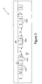
- the ideal electric field profile of an ideal Multiple Floating Guard Rings (MFGR) termination is shown in Figures 1A through 1D.
- Figure 1A illustrates a conventional MFGR device where the spacing between the p-type SiC guard rings is illustrated as constant for simplicity. At the blocking state, the depletion region starts at the main junction and expands both laterally and vertically. Once the depletion region punches through to the first guard ring, the potential of the first guard ring gets pinned to that of the main junction.
- the punch-through side of the guard ring injects a small amount of holes into the n-region. This lost charge is replaced by the depletion of the n charge from the outer edge of the guard ring. This punch-through and charge injection continues on until the depletion region reaches the final guard ring. Since the amounts of n-charge depleted between the guard rings are the same (constant spacing MFGR's), the peak x-field each guard ring sees is the same for all guard rings, as shown in Figure 1B . However, as seen in Figure 1C , the peak y-field is different for all guard rings because the amount of n-charge depletion is different for all guard rings.
- the highest y-field value is present at the main junction and successive guard rings have reduced levels of y-field.
- the vector sum of the x and the y fields is illustrated in Figure 1D , and shows the highest electric field at the bottom corner of the main junction (circled in Figure 1A ). Therefore, breakdown is expected to happen at the circled bottom edge of the main junction if equally spaced MFGR termination is used. If it is desired that each floating guard ring supports the same electric fields, the spacing between the guard rings may vary. The spacing between the main junction and the inner-most guard ring may be the smallest, and the spacing at the outer-most guarding may be the largest.
- MOS metal-oxide-semiconductor
- Breakdown walk-out refers to a phenomenon where the breakdown voltage starts at a first value and increases with time and bias. This problem may be even greater in silicon carbide devices because the field oxides are generally deposited. Deposited oxides, typically, have inferior characteristics to those of thermally grown layers, and the oxide-semiconductor interface in a silicon carbide device has much greater charge density compared to that of a silicon device.
- an n-type semiconductor layer 10 has a main junction 12 and a series of floating guard rings 14 formed therein.
- An oxide layer 16 is provided on the semiconductor layer 10 and openings are provided in the oxide layer 16.
- the offset field plates 18 are provided in the openings to contact the floating guard rings 14 and to extend onto the oxide layer 16.
- Offset Field Plate-Floating Guard Ring structure has each field plate contacting each guard ring separately and the edge of the guard ring should not overlap with the edge of the next guard ring.
- each guard ring may need to be enlarged, and the alignment tolerance of the guard rings should be less than 0.25 ⁇ m.
- Step coverage may also be another issue with the Offset Field Plate-Floating Guard Ring structure because the thickness of the oxide that may be needed.
- the quality of the oxide may be important in achieving acceptable results as it is the oxide that supports the field or voltages. Oxides in silicon carbide devices, generally have lower quality than that available in silicon devices. Accordingly, the Offset Field Plate-Floating Guard Ring structure may not be practical for silicon carbide devices.
- Guard ring edge termination structures suitable for use in silicon carbide devices are discussed in commonly assigned United States Patent No. 7,026,650 issued on April 11, 2006 to Ryu et al. entitled Multiple floating guard ring edge termination for silicon carbide devices, the disclosure of which is hereby incorporated herein by reference in its entirety.
- a surface charge compensation layer such as a thin p-type layer, is provided in addition to the multiple floating guard rings.
- the surface charge compensation layer may be used to at least partially neutralize the effects of charges at oxide-semiconductor interfaces in the silicon carbide devices.
- the present invention provides an edge termination structure according to claim 1 and a method of fabricating an edge termination structure according to claim 14.
- embodiments of the present invention may provide improved edge termination of semiconductor devices, such as P-N, Schottky, PiN or other such semiconductor devices.
- semiconductor devices such as P-N, Schottky, PiN or other such semiconductor devices.
- Particular embodiments of the present invention provide edge termination for silicon carbide (SiC) devices.
- SiC silicon carbide
- embodiments of the present invention may be utilized as edge termination for SiC Schottky diodes, junction barrier Schottky (JBS) diodes, PiN diodes, thyristors, transistors, or other such SiC devices without departing from the scope of the present invention.
- JBS junction barrier Schottky
- the present invention provides an improved edge termination for high voltage silicon carbide devices using double guard ring termination ("double GR termination”) as will be discussed in detail below with respect to Figures 13 through 15 .
- United States Patent No. 7,026,650 to Ryu et al. discusses robust guard ring termination ("robust GR termination") used in conjuction with SiC power devices.
- a surface charge compensation layer such as a thin p-type layer, is provided in addition to the multiple floating guard rings.
- the guard ring termination structure discussed in the '650 patent has shown higher blocking capabilities than the conventional guard ring termination, including junction termination extension (JTE). However, the maximum breakdown voltage may still be less than the value predicted in theory.
- some conventional structures provide double guard ring (DGR) termination structures for highly doped and lightly doped implantations, respectively.
- the highly doped portion of the guard ring may be achieved by Aluminum (Al) implants, while the lightly doped portion of the guard ring may be achieved by Boron (B) implant.
- Providing both highly doped and lightly doped implants may provide a doping gradient from the main junction to the termination edge such that the electrical field can be further reduced.
- the mean doping concentration of the guard ring is greater at the main junction of the device and decreases toward the periphery of the device.
- the doping gradient is especially useful for Boron in SiC, which can diffuse during a high temperature activation process. Details will be discussed further herein with respect to Figures 3 through 15 .
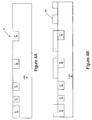
- a silicon carbide layer 30 such as a lightly doped n-type silicon carbide layer, has formed therein a main junction 32, for example, of p-type silicon carbide, and a plurality of double guard rings DGR1, DGR2, DGR3 and DGR4, such as p-type silicon carbide floating guard rings.
- an insulating layer 26, such as an oxide layer, is provided on the silicon carbide layer 30.
- the insulating layer 26 may be a deposited or grown oxide and may be fabricated utilizing techniques known to those of skill in the art.
- the insulating layer 26 may be an oxide, such as SiO 2 , a nitride, such as Si 3 N 4 , an oxide-nitride-oxide structure and/or an oxynitride or organic films such as a polyimide layer.
- the double guard rings DGR1, DGR2, DGR3 and DGR4 each include first and second portions 34 and 36, respectively.
- the first and second portions 34 and 36 of the double guard rings DGR1, DGR2, DGR3 and DGR4 may be p-type silicon carbide. Further illustrated are the distances between the second DGR2 and third guard DGR3 rings and the third DGR3 and fourth DGR4 guard rings D2 and D3, respectively.
- the lightly doped portion (p - ) 36 may be from about 5.0X10 16 to about 5.0x10 17 cm -3 .
- n + " or "p + " refer to regions that are defined by higher carrier concentrations than are present in adjacent or other regions of the same or another layer or substrate.
- the highly doped portions 34 and the lightly doped portions 36 of the double guard rings DGR1, DGR2; DGR3 and DGR4 may extend a distance D4 from about 0.3 to about 0.8 ⁇ m into the silicon carbide layer 30.
- the highly doped 34 and/or lightly doped 36 portions of the double guard rings DGR1, DGR2, DGR3 and DGR4 may have higher doping concentrations closer to the main junction 32 of the device 20 and lower doping concentrations at the periphery of the device 20.
- Aluminum ions are implanted to achieve the highly doped portions 34 and Boron ions are implanted to achieve the lightly doped portions 36.
- Providing the lightly doped portions 36 in a second guard ring adjacent the highly doped guard ring allows a doping gradient from the main junction 32 to the termination edge to be provided, especially for Boron in SiC which can diffuse during high temperature activation process. Thus, the electric field may be further reduced.
- the oxide-semiconductor interface is expected to have from about 1.0x10 12 to about 2.0x10 12 cm -3 of positive charge.
- the surface of the surface low does portions 36 of the double guard rings DGR1, DGR2, DGR3 and DGR4 will, typically, be depleted by the positive surface charges, and the negative charges in the depletion region low does portions 36 of the double guard rings DGR1, DGR2, DGR3 and DGR4 will reduce the E-field lines originating from the oxide interface charges, and possibly neutralize the negative effects of the positive interface charges.
- the double guard rings 34/36 may be uniformly spaced, non-uniformly spaced or combinations of uniformly and non-uniformly spaced. In other words, the lengths of D1, D2, D3 and the like may vary and may not be constant. Additionally, in certain conventional structures, from about 1 to about 100 guard rings 34/36 may be provided. The guard rings 34/36 may extend a distance of from about 10 ⁇ m to about 1000 ⁇ m from the main junction of the device.
- the lightly doped portions 36 may be formed before or after formation of the highly doped portions 34. Both the highly doped portion 34 and the lightly doped portion 36 may be provided by, for example, ion implantation, or other techniques known to those of skill in the art. Alternatively, the lightly doped portion 34 or the highly doped portion 36 may be an epitaxially grown layer of SiC or deposited layer of SiC that is formed on the layer 30 and, in the case of the regions, patterned to provide the desired surface charge compensation regions and/or layers. In such case, the guard rings may be formed prior to formation of the SiC layer or after formation of the SiC layer.
- edge termination techniques may be utilized with other devices and/or junction types, such as Schottky junctions.
- some conventional structures provide a novel edge termination structure including double guard rings for the high and low implant doses to further reduce the electrical field.
- some conventional structures provide a gradient of the lightly doped portion 34 of the guard ring, which can further improve the blocking capability of power devices.
- the lightly doped portion 34 may have a wide range of tolerance in processing such as misalignment, opening definition, and the like.
- Double guard ring termination structures according to some conventional structures may be processed using existing processes and, therefore, may not increase the processing steps and difficulty of processing these devices.
- a higher blocking capability provided by devices according to some conventional structures may result in the improvement in other parameters of power devices, such as reducing on-resistance by a thinner drift layer.
- a thinner drift layer may reduce the power device die size further to achieve a higher die yield.
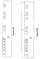
- a silicon carbide layer 30 has formed in it a junction 32 and spaced apart highly doped portions 34 of the double guard ring structure.
- Such regions may be formed, for example, by ion implantation into a silicon carbide substrate and/or epitaxial layer.
- aluminum ions having a doping concentration of from about 5.0x10 18 to about 1.0x10 20 cm -3 may be implanted into the silicon carbide layer 30 to provide the highly doped portions 34 illustrated in Figure 4A .
- a mask layer 100 may be formed and patterned on the silicon carbide layer 30 and may correspond to the junction 32 and highly doped portions of the guard ring 34.
- the mask layer 100 may be made of conventional mask materials and may, for example, be patterned using conventional photolithography or other such techniques known to those of skill in the art.
- the mask layer 100 opens windows adjacent the junction 32 and the highly doped portions of the guard rings 34.
- the lightly doped portions 36 of the guard rings may be formed through ion implantation using the mask layer 100 as an ion implantation mask.
- boron ions having a doping concentration of from about 5.0x 10 16 to about 5.0x10 17 cm -3 may be implanted into the silicon carbide layer 30 to provide the lightly doped portions 34 illustrated in Figure 4C .
- the mask layer 100 may then be removed and the insulating layer 26 may be formed on the resulting structure as illustrated in Figure 4D .
- the insulating layer 26 may, for example, be formed by thermal oxidation and/or depositing an oxide on the resulting structure.
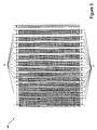
- double guard ring termination structures in accordance with some conventional structures will be discussed.
- the mask 500 has been patterned to form the lightly doped portion 34, for example, boron, of the double guard rings and the highly doped portion 36, for example, aluminum, of the double guard rings.
- the portions of the mask 500 used to implant the highly doped portions 36 are set out in Figure 5 .
- the portions of the mask 500 used to implant the lightly doped portions 34 are set out in Figure 5 .
- double guard ring termination in accordance with some conventional structures may allow the dose of the lightly doped guard ring (B) to be gradually reduced from the main junction of the device to the periphery using one time implantation.
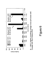
- FIG. 6 a blocking histogram for diodes with robust guard ring termination and double guard ring termination according to some conventional structures will be discussed. As illustrated by the histogram, a blocking voltage of about 130 V higher was achieved using the double guard ring termination structure.
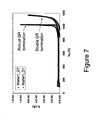
- Figure 7 is a graph illustrating representative reverse IV curves for diodes with robust guard ring termination and double guard ring termination according to some conventional structures.
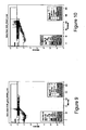
- Figure 8 is a graph illustrating simulations of SiC JBS diode blocking characteristics for diodes with robust guard ring termination and double guard ring termination according to some conventional structures. The devices were fabricated using the same wafer.
- Figures 9 and 10 are graphs illustrating potential distribution of JBS with double guard ring termination and robust guard ring termination at 680V, respectively, according to some conventional structures.
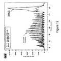
- Figures 11 and 12 are graphs illustrating electrical field distribution comparisons underneath termination junctions, and at the SiO 2 /SiC interface, respectively, according to some conventional structures. It will be understood that a lower electric field yields a lower leakage current.
- the lightly doped portion of the double guard ring structure has first and second portions 46 and 47.
- the first portion of the lightly doped portion 46 may be a p -- layer and may have a doping concentration of about 1.0 x 10 17 cm -3 .
- the first portion of the lightly doped portion may extend about 0.5 ⁇ m into the semiconductor layer 30.
- the second portion of the lightly doped portion 47 may be a p - layer and have a doping concentration of about 1.4 x10 17 cm -3 .
- the second portion of the lightly dopes portion 47 may extend about 0.8 ⁇ m into the semiconductor layer 30 and may extend beneath the highly doped portion 36.
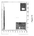
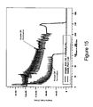
- the present invention illustrated in Figure 13 may exhibit improvement in electric field characteristics as illustrated in Figures 14 and 15 discussed below.
- Figure 14 is a graph illustrating electric field characteristics in accordance with the present invention illustrated in Figure 13 .
- Figure 15 is a graph illustrating electric field characteristics in accordance with the present invention illustrated in Figure 13 .
- Figure 15 is a graph illustrating robust GR termination and double guard ring termination with a retrograde profile of the second doping concentration.
- embodiments of the present invention are discussed above primarily with respect to silicon carbide semiconductor devices, embodiments of the present invention are not limited to silicon carbide devices.
- devices according to some embodiments of the present invention may be silicon (Si), gallium nitride (GaN) or gallium arsenide (GaAs) without departing from the scope of the present invention.
Landscapes
- Electrodes Of Semiconductors (AREA)
Applications Claiming Priority (2)
| Application Number | Priority Date | Filing Date | Title |
|---|---|---|---|
| US12/037,211 US9640609B2 (en) | 2008-02-26 | 2008-02-26 | Double guard ring edge termination for silicon carbide devices |
| PCT/US2009/000734 WO2009108268A1 (en) | 2008-02-26 | 2009-02-05 | Double guard ring edge termination for silicon carbide devices and methods of fabricating silicon carbide devices incorporating same |
Publications (2)
| Publication Number | Publication Date |
|---|---|
| EP2248176A1 EP2248176A1 (en) | 2010-11-10 |
| EP2248176B1 true EP2248176B1 (en) | 2014-04-23 |
Family
ID=40524779
Family Applications (1)
| Application Number | Title | Priority Date | Filing Date |
|---|---|---|---|
| EP09713922.4A Active EP2248176B1 (en) | 2008-02-26 | 2009-02-05 | Double guard ring edge termination for silicon carbide devices and methods of fabricating silicon carbide devices incorporating same |
Country Status (6)
| Country | Link |
|---|---|
| US (1) | US9640609B2 (enExample) |
| EP (1) | EP2248176B1 (enExample) |
| JP (1) | JP5324603B2 (enExample) |
| KR (1) | KR101595587B1 (enExample) |
| CN (1) | CN101981700B (enExample) |
| WO (1) | WO2009108268A1 (enExample) |
Families Citing this family (55)
| Publication number | Priority date | Publication date | Assignee | Title |
|---|---|---|---|---|
| US8432012B2 (en) | 2006-08-01 | 2013-04-30 | Cree, Inc. | Semiconductor devices including schottky diodes having overlapping doped regions and methods of fabricating same |
| US7728402B2 (en) | 2006-08-01 | 2010-06-01 | Cree, Inc. | Semiconductor devices including schottky diodes with controlled breakdown |
| EP2631951B1 (en) | 2006-08-17 | 2017-10-11 | Cree, Inc. | High power insulated gate bipolar transistors |
| US8835987B2 (en) | 2007-02-27 | 2014-09-16 | Cree, Inc. | Insulated gate bipolar transistors including current suppressing layers |
| US9640609B2 (en) | 2008-02-26 | 2017-05-02 | Cree, Inc. | Double guard ring edge termination for silicon carbide devices |
| US8232558B2 (en) | 2008-05-21 | 2012-07-31 | Cree, Inc. | Junction barrier Schottky diodes with current surge capability |
| US8097919B2 (en) | 2008-08-11 | 2012-01-17 | Cree, Inc. | Mesa termination structures for power semiconductor devices including mesa step buffers |
| US8637386B2 (en) * | 2009-05-12 | 2014-01-28 | Cree, Inc. | Diffused junction termination structures for silicon carbide devices and methods of fabricating silicon carbide devices incorporating same |
| US8193848B2 (en) | 2009-06-02 | 2012-06-05 | Cree, Inc. | Power switching devices having controllable surge current capabilities |
| US8629509B2 (en) | 2009-06-02 | 2014-01-14 | Cree, Inc. | High voltage insulated gate bipolar transistors with minority carrier diverter |
| US8999245B2 (en) | 2009-07-07 | 2015-04-07 | Tricorn Tech Corporation | Cascaded gas chromatographs (CGCs) with individual temperature control and gas analysis systems using same |
| US8541787B2 (en) | 2009-07-15 | 2013-09-24 | Cree, Inc. | High breakdown voltage wide band-gap MOS-gated bipolar junction transistors with avalanche capability |
| US8707760B2 (en) | 2009-07-31 | 2014-04-29 | Tricorntech Corporation | Gas collection and analysis system with front-end and back-end pre-concentrators and moisture removal |
| US8354690B2 (en) | 2009-08-31 | 2013-01-15 | Cree, Inc. | Solid-state pinch off thyristor circuits |
| EP2341528A1 (en) * | 2010-01-05 | 2011-07-06 | ABB Technology AG | Power Semiconductor Device and its manufacturing method |
| US9117739B2 (en) | 2010-03-08 | 2015-08-25 | Cree, Inc. | Semiconductor devices with heterojunction barrier regions and methods of fabricating same |
| US8415671B2 (en) | 2010-04-16 | 2013-04-09 | Cree, Inc. | Wide band-gap MOSFETs having a heterojunction under gate trenches thereof and related methods of forming such devices |
| US8978444B2 (en) | 2010-04-23 | 2015-03-17 | Tricorn Tech Corporation | Gas analyte spectrum sharpening and separation with multi-dimensional micro-GC for gas chromatography analysis |
| DE112011103469B4 (de) * | 2010-10-15 | 2023-01-19 | Mitsubishi Electric Corporation | Halbleitervorrichtung |
| US8803277B2 (en) * | 2011-02-10 | 2014-08-12 | Cree, Inc. | Junction termination structures including guard ring extensions and methods of fabricating electronic devices incorporating same |
| JP5558393B2 (ja) * | 2011-03-10 | 2014-07-23 | 株式会社東芝 | 半導体装置 |
| US9673283B2 (en) | 2011-05-06 | 2017-06-06 | Cree, Inc. | Power module for supporting high current densities |
| US9142662B2 (en) | 2011-05-06 | 2015-09-22 | Cree, Inc. | Field effect transistor devices with low source resistance |
| US9029945B2 (en) | 2011-05-06 | 2015-05-12 | Cree, Inc. | Field effect transistor devices with low source resistance |
| CN102263139A (zh) * | 2011-05-24 | 2011-11-30 | 哈尔滨工程大学 | 一种改进的混合整流二极管结构 |
| US9373617B2 (en) | 2011-09-11 | 2016-06-21 | Cree, Inc. | High current, low switching loss SiC power module |
| US8680587B2 (en) | 2011-09-11 | 2014-03-25 | Cree, Inc. | Schottky diode |
| US9640617B2 (en) | 2011-09-11 | 2017-05-02 | Cree, Inc. | High performance power module |
| US8618582B2 (en) | 2011-09-11 | 2013-12-31 | Cree, Inc. | Edge termination structure employing recesses for edge termination elements |
| US8664665B2 (en) | 2011-09-11 | 2014-03-04 | Cree, Inc. | Schottky diode employing recesses for elements of junction barrier array |
| JP6132478B2 (ja) * | 2012-05-09 | 2017-05-24 | 三菱電機株式会社 | 半導体装置 |
| US8901639B2 (en) | 2012-07-26 | 2014-12-02 | Cree, Inc. | Monolithic bidirectional silicon carbide switching devices |
| WO2014045480A1 (ja) * | 2012-09-21 | 2014-03-27 | 三菱電機株式会社 | 半導体装置及び半導体装置の製造方法 |
| JP6029411B2 (ja) | 2012-10-02 | 2016-11-24 | 三菱電機株式会社 | 半導体装置 |
| JP6090988B2 (ja) | 2013-03-05 | 2017-03-08 | 株式会社 日立パワーデバイス | 半導体装置 |
| JP6079456B2 (ja) * | 2013-06-07 | 2017-02-15 | 三菱電機株式会社 | 半導体装置の検査方法 |
| US9064738B2 (en) * | 2013-07-19 | 2015-06-23 | Cree, Inc. | Methods of forming junction termination extension edge terminations for high power semiconductor devices and related semiconductor devices |
| JP6183234B2 (ja) * | 2014-01-30 | 2017-08-23 | 富士電機株式会社 | 半導体装置および半導体装置の製造方法 |
| JP6265274B2 (ja) * | 2014-09-17 | 2018-01-24 | 富士電機株式会社 | 半導体装置 |
| EP3012870A1 (en) * | 2014-10-20 | 2016-04-27 | ABB Technology AG | Edge termination for high voltage semiconductor devices |
| JP2015079987A (ja) * | 2014-12-17 | 2015-04-23 | 株式会社日立製作所 | 半導体装置 |
| WO2016198388A1 (en) | 2015-06-09 | 2016-12-15 | Abb Schweiz Ag | Method for manufacturing an edge termination for a silicon carbide power semiconductor device |
| CN108369963B (zh) * | 2015-12-15 | 2022-01-25 | 通用电气公司 | 碳化硅超结功率器件的边缘终端设计 |
| JP6649198B2 (ja) * | 2016-07-14 | 2020-02-19 | トヨタ自動車株式会社 | 半導体装置とその製造方法 |
| JP6673174B2 (ja) | 2016-12-12 | 2020-03-25 | 株式会社デンソー | 炭化珪素半導体装置およびその製造方法 |
| US10312710B1 (en) | 2017-01-31 | 2019-06-04 | The United States Of America, As Represented By The Secretary Of The Navy | Energy recovery pulse forming network |
| JP6233537B2 (ja) * | 2017-02-27 | 2017-11-22 | 富士電機株式会社 | 半導体装置および半導体装置の製造方法 |
| JP6336165B2 (ja) * | 2017-03-14 | 2018-06-06 | 三菱電機株式会社 | 半導体装置 |
| DE102017127848B4 (de) * | 2017-11-24 | 2024-10-17 | Infineon Technologies Ag | Siliziumcarbid-Halbleiterbauelement mit Randabschlussstruktur |
| US10418402B2 (en) * | 2017-11-30 | 2019-09-17 | Stmicroelectronics (Research & Development) Limited | Near ultraviolet photocell |
| JP7132719B2 (ja) * | 2018-01-19 | 2022-09-07 | ローム株式会社 | 半導体装置 |
| CN109087940A (zh) * | 2018-09-11 | 2018-12-25 | 无锡新洁能股份有限公司 | 一种SiC功率器件终端及其制作方法 |
| US20220157951A1 (en) | 2020-11-17 | 2022-05-19 | Hamza Yilmaz | High voltage edge termination structure for power semicondcutor devices and manufacturing method thereof |
| KR102372131B1 (ko) * | 2020-11-27 | 2022-03-08 | 재단법인 부산테크노파크 | 고내압 실리콘 카바이드 쇼트키 베리어 다이오드 및 제조방법 |
| EP4517827A1 (en) * | 2023-08-28 | 2025-03-05 | Nexperia B.V. | A semiconductor device having an improved termination area, as well as a corresponding method and power device |
Family Cites Families (50)
| Publication number | Priority date | Publication date | Assignee | Title |
|---|---|---|---|---|
| US4242690A (en) | 1978-06-06 | 1980-12-30 | General Electric Company | High breakdown voltage semiconductor device |
| DE3581348D1 (de) | 1984-09-28 | 1991-02-21 | Siemens Ag | Verfahren zum herstellen eines pn-uebergangs mit hoher durchbruchsspannung. |
| US4742377A (en) * | 1985-02-21 | 1988-05-03 | General Instrument Corporation | Schottky barrier device with doped composite guard ring |
| EP0389863B1 (de) | 1989-03-29 | 1996-12-18 | Siemens Aktiengesellschaft | Verfahren zur Herstellung eines planaren pn-Übergangs hoher Spannungsfestigkeit |
| US4927772A (en) | 1989-05-30 | 1990-05-22 | General Electric Company | Method of making high breakdown voltage semiconductor device |
| GB8913198D0 (en) * | 1989-06-08 | 1989-07-26 | British Telecomm | Guard ring structure |
| JPH0362422A (ja) | 1989-07-31 | 1991-03-18 | Showa Electric Wire & Cable Co Ltd | 水密型撚線導体の製造方法 |
| JPH03225870A (ja) | 1990-01-31 | 1991-10-04 | Toshiba Corp | ヘテロ接合バイポーラトランジスタの製造方法 |
| JPH0492434A (ja) | 1990-08-08 | 1992-03-25 | Sumitomo Electric Ind Ltd | ヘテロ接合バイポーラトランジスタの製造方法 |
| CN1040814C (zh) | 1994-07-20 | 1998-11-18 | 电子科技大学 | 一种用于半导体器件的表面耐压区 |
| TW286435B (enExample) | 1994-07-27 | 1996-09-21 | Siemens Ag | |
| US5967795A (en) | 1995-08-30 | 1999-10-19 | Asea Brown Boveri Ab | SiC semiconductor device comprising a pn junction with a voltage absorbing edge |
| JP3997551B2 (ja) * | 1995-12-08 | 2007-10-24 | 株式会社日立製作所 | プレーナ型半導体装置 |
| SE9602745D0 (sv) * | 1996-07-11 | 1996-07-11 | Abb Research Ltd | A method for producing a channel region layer in a SiC-layer for a voltage controlled semiconductor device |
| US6002159A (en) | 1996-07-16 | 1999-12-14 | Abb Research Ltd. | SiC semiconductor device comprising a pn junction with a voltage absorbing edge |
| SE9700156D0 (sv) * | 1997-01-21 | 1997-01-21 | Abb Research Ltd | Junction termination for Si C Schottky diode |
| SE9802909L (sv) * | 1998-08-31 | 1999-10-13 | Abb Research Ltd | Metod för framställning av en pn-övergång för en halvledaranordning av SiC samt en halvledaranordning av SiC med pn-övergång |
| JP2002535840A (ja) * | 1999-01-12 | 2002-10-22 | オイペツク オイロペーイツシエ ゲゼルシヤフト フユール ライスツングスハルプライター エムベーハー ウント コンパニイ コマンデイートゲゼルシヤフト | メサ形縁端部を備えるパワー半導体素子 |
| JP2001035857A (ja) | 1999-07-21 | 2001-02-09 | Nec Corp | 化合物ヘテロバイポーラトランジスタおよびその製造方法 |
| JP2001196604A (ja) | 2000-01-12 | 2001-07-19 | Hitachi Ltd | 半導体装置 |
| JP4839519B2 (ja) * | 2001-03-15 | 2011-12-21 | 富士電機株式会社 | 半導体装置 |
| CN100483733C (zh) | 2003-01-15 | 2009-04-29 | 克里公司 | 碳化硅器件的边缘环形端接 |
| US7026650B2 (en) * | 2003-01-15 | 2006-04-11 | Cree, Inc. | Multiple floating guard ring edge termination for silicon carbide devices |
| US7109521B2 (en) * | 2004-03-18 | 2006-09-19 | Cree, Inc. | Silicon carbide semiconductor structures including multiple epitaxial layers having sidewalls |
| DE102004045768B4 (de) | 2004-09-21 | 2007-01-04 | Infineon Technologies Ag | Verfahren zur Herstellung eines Randabschlusses eines Halbleiterbauelements |
| US7144797B2 (en) * | 2004-09-24 | 2006-12-05 | Rensselaer Polytechnic Institute | Semiconductor device having multiple-zone junction termination extension, and method for fabricating the same |
| JP3914226B2 (ja) | 2004-09-29 | 2007-05-16 | 株式会社東芝 | 高耐圧半導体装置 |
| US7498651B2 (en) * | 2004-11-24 | 2009-03-03 | Microsemi Corporation | Junction termination structures for wide-bandgap power devices |
| US7304363B1 (en) * | 2004-11-26 | 2007-12-04 | United States Of America As Represented By The Secretary Of The Army | Interacting current spreader and junction extender to increase the voltage blocked in the off state of a high power semiconductor device |
| JP2006196652A (ja) | 2005-01-13 | 2006-07-27 | Shindengen Electric Mfg Co Ltd | SiC半導体素子 |
| DE102005023668B3 (de) * | 2005-05-23 | 2006-11-09 | Infineon Technologies Ag | Halbleiterbauelement mit einer Randstruktur mit Spannungsdurchbruch im linearen Bereich |
| JP4755854B2 (ja) * | 2005-06-02 | 2011-08-24 | 富士通株式会社 | 半導体受光装置及びその製造方法 |
| JP4777699B2 (ja) | 2005-06-13 | 2011-09-21 | 本田技研工業株式会社 | バイポーラ型半導体装置およびその製造方法 |
| US8084815B2 (en) * | 2005-06-29 | 2011-12-27 | Fairchild Korea Semiconductor Ltd. | Superjunction semiconductor device |
| US7304334B2 (en) | 2005-09-16 | 2007-12-04 | Cree, Inc. | Silicon carbide bipolar junction transistors having epitaxial base regions and multilayer emitters and methods of fabricating the same |
| CN100461408C (zh) | 2005-09-28 | 2009-02-11 | 中芯国际集成电路制造(上海)有限公司 | 带有密封环拐角结构的集成电路器件 |
| JP2007096006A (ja) | 2005-09-29 | 2007-04-12 | Nippon Inter Electronics Corp | ガードリングの製造方法および半導体装置 |
| JP2007103784A (ja) * | 2005-10-06 | 2007-04-19 | Matsushita Electric Ind Co Ltd | ヘテロ接合バイポーラトランジスタ |
| JP2007115875A (ja) | 2005-10-20 | 2007-05-10 | Sumitomo Electric Ind Ltd | 炭化珪素半導体装置およびその製造方法 |
| JP5044117B2 (ja) | 2005-12-14 | 2012-10-10 | 関西電力株式会社 | 炭化珪素バイポーラ型半導体装置 |
| US7345310B2 (en) | 2005-12-22 | 2008-03-18 | Cree, Inc. | Silicon carbide bipolar junction transistors having a silicon carbide passivation layer on the base region thereof |
| JP2007287782A (ja) * | 2006-04-13 | 2007-11-01 | Hitachi Ltd | メサ型バイポーラトランジスタ |
| US7372087B2 (en) * | 2006-06-01 | 2008-05-13 | Northrop Grumman Corporation | Semiconductor structure for use in a static induction transistor having improved gate-to-drain breakdown voltage |
| WO2008005092A2 (en) * | 2006-06-29 | 2008-01-10 | Cree, Inc. | Silicon carbide switching devices including p-type channels and methods of forming the same |
| EP2631951B1 (en) * | 2006-08-17 | 2017-10-11 | Cree, Inc. | High power insulated gate bipolar transistors |
| KR101494935B1 (ko) * | 2007-11-09 | 2015-02-23 | 크리,인코포레이티드 | 메사 스텝들을 포함하는 버퍼층들 및 메사 구조들을 가지는 전력 반도체 장치들 |
| JP2009164486A (ja) | 2008-01-09 | 2009-07-23 | Toyota Motor Corp | 縦型ダイオードとその製造方法 |
| US9640609B2 (en) | 2008-02-26 | 2017-05-02 | Cree, Inc. | Double guard ring edge termination for silicon carbide devices |
| US8097919B2 (en) * | 2008-08-11 | 2012-01-17 | Cree, Inc. | Mesa termination structures for power semiconductor devices including mesa step buffers |
| US8637386B2 (en) * | 2009-05-12 | 2014-01-28 | Cree, Inc. | Diffused junction termination structures for silicon carbide devices and methods of fabricating silicon carbide devices incorporating same |
-
2008
- 2008-02-26 US US12/037,211 patent/US9640609B2/en active Active
-
2009
- 2009-02-05 KR KR1020107021354A patent/KR101595587B1/ko active Active
- 2009-02-05 CN CN200980111322.0A patent/CN101981700B/zh active Active
- 2009-02-05 EP EP09713922.4A patent/EP2248176B1/en active Active
- 2009-02-05 JP JP2010548670A patent/JP5324603B2/ja active Active
- 2009-02-05 WO PCT/US2009/000734 patent/WO2009108268A1/en not_active Ceased
Also Published As
| Publication number | Publication date |
|---|---|
| JP5324603B2 (ja) | 2013-10-23 |
| KR20100128303A (ko) | 2010-12-07 |
| US9640609B2 (en) | 2017-05-02 |
| WO2009108268A1 (en) | 2009-09-03 |
| KR101595587B1 (ko) | 2016-02-18 |
| CN101981700B (zh) | 2014-05-14 |
| JP2011514674A (ja) | 2011-05-06 |
| CN101981700A (zh) | 2011-02-23 |
| EP2248176A1 (en) | 2010-11-10 |
| US20090212301A1 (en) | 2009-08-27 |
Similar Documents
| Publication | Publication Date | Title |
|---|---|---|
| EP2248176B1 (en) | Double guard ring edge termination for silicon carbide devices and methods of fabricating silicon carbide devices incorporating same | |
| US8124480B2 (en) | Methods of fabricating silicon carbide devices incorporating multiple floating guard ring edge terminations | |
| EP1974387B1 (en) | Edge termination structures for silicon carbide devices and methods of fabricating silicon carbide devices incorporating same | |
| US9318623B2 (en) | Recessed termination structures and methods of fabricating electronic devices including recessed termination structures | |
| US11271076B2 (en) | Systems and methods for junction termination in semiconductor devices |
Legal Events
| Date | Code | Title | Description |
|---|---|---|---|
| PUAI | Public reference made under article 153(3) epc to a published international application that has entered the european phase |
Free format text: ORIGINAL CODE: 0009012 |
|
| 17P | Request for examination filed |
Effective date: 20100903 |
|
| AK | Designated contracting states |
Kind code of ref document: A1 Designated state(s): AT BE BG CH CY CZ DE DK EE ES FI FR GB GR HR HU IE IS IT LI LT LU LV MC MK MT NL NO PL PT RO SE SI SK TR |
|
| AX | Request for extension of the european patent |
Extension state: AL BA RS |
|
| DAX | Request for extension of the european patent (deleted) | ||
| 17Q | First examination report despatched |
Effective date: 20120113 |
|
| GRAP | Despatch of communication of intention to grant a patent |
Free format text: ORIGINAL CODE: EPIDOSNIGR1 |
|
| INTG | Intention to grant announced |
Effective date: 20131111 |
|
| GRAS | Grant fee paid |
Free format text: ORIGINAL CODE: EPIDOSNIGR3 |
|
| GRAA | (expected) grant |
Free format text: ORIGINAL CODE: 0009210 |
|
| AK | Designated contracting states |
Kind code of ref document: B1 Designated state(s): AT BE BG CH CY CZ DE DK EE ES FI FR GB GR HR HU IE IS IT LI LT LU LV MC MK MT NL NO PL PT RO SE SI SK TR |
|
| REG | Reference to a national code |
Ref country code: GB Ref legal event code: FG4D |
|
| REG | Reference to a national code |
Ref country code: CH Ref legal event code: EP Ref country code: CH Ref legal event code: NV Representative=s name: KIRKER AND CIE S.A., CH |
|
| REG | Reference to a national code |
Ref country code: AT Ref legal event code: REF Ref document number: 664276 Country of ref document: AT Kind code of ref document: T Effective date: 20140515 |
|
| REG | Reference to a national code |
Ref country code: IE Ref legal event code: FG4D |
|
| REG | Reference to a national code |
Ref country code: DE Ref legal event code: R096 Ref document number: 602009023450 Country of ref document: DE Effective date: 20140605 |
|
| REG | Reference to a national code |
Ref country code: NL Ref legal event code: VDEP Effective date: 20140423 |
|
| REG | Reference to a national code |
Ref country code: LT Ref legal event code: MG4D |
|
| PG25 | Lapsed in a contracting state [announced via postgrant information from national office to epo] |
Ref country code: CY Free format text: LAPSE BECAUSE OF FAILURE TO SUBMIT A TRANSLATION OF THE DESCRIPTION OR TO PAY THE FEE WITHIN THE PRESCRIBED TIME-LIMIT Effective date: 20140423 Ref country code: NL Free format text: LAPSE BECAUSE OF FAILURE TO SUBMIT A TRANSLATION OF THE DESCRIPTION OR TO PAY THE FEE WITHIN THE PRESCRIBED TIME-LIMIT Effective date: 20140423 Ref country code: BG Free format text: LAPSE BECAUSE OF FAILURE TO SUBMIT A TRANSLATION OF THE DESCRIPTION OR TO PAY THE FEE WITHIN THE PRESCRIBED TIME-LIMIT Effective date: 20140723 Ref country code: LT Free format text: LAPSE BECAUSE OF FAILURE TO SUBMIT A TRANSLATION OF THE DESCRIPTION OR TO PAY THE FEE WITHIN THE PRESCRIBED TIME-LIMIT Effective date: 20140423 Ref country code: GR Free format text: LAPSE BECAUSE OF FAILURE TO SUBMIT A TRANSLATION OF THE DESCRIPTION OR TO PAY THE FEE WITHIN THE PRESCRIBED TIME-LIMIT Effective date: 20140724 Ref country code: IS Free format text: LAPSE BECAUSE OF FAILURE TO SUBMIT A TRANSLATION OF THE DESCRIPTION OR TO PAY THE FEE WITHIN THE PRESCRIBED TIME-LIMIT Effective date: 20140823 Ref country code: NO Free format text: LAPSE BECAUSE OF FAILURE TO SUBMIT A TRANSLATION OF THE DESCRIPTION OR TO PAY THE FEE WITHIN THE PRESCRIBED TIME-LIMIT Effective date: 20140723 Ref country code: FI Free format text: LAPSE BECAUSE OF FAILURE TO SUBMIT A TRANSLATION OF THE DESCRIPTION OR TO PAY THE FEE WITHIN THE PRESCRIBED TIME-LIMIT Effective date: 20140423 |
|
| PG25 | Lapsed in a contracting state [announced via postgrant information from national office to epo] |
Ref country code: ES Free format text: LAPSE BECAUSE OF FAILURE TO SUBMIT A TRANSLATION OF THE DESCRIPTION OR TO PAY THE FEE WITHIN THE PRESCRIBED TIME-LIMIT Effective date: 20140423 Ref country code: PL Free format text: LAPSE BECAUSE OF FAILURE TO SUBMIT A TRANSLATION OF THE DESCRIPTION OR TO PAY THE FEE WITHIN THE PRESCRIBED TIME-LIMIT Effective date: 20140423 Ref country code: LV Free format text: LAPSE BECAUSE OF FAILURE TO SUBMIT A TRANSLATION OF THE DESCRIPTION OR TO PAY THE FEE WITHIN THE PRESCRIBED TIME-LIMIT Effective date: 20140423 Ref country code: HR Free format text: LAPSE BECAUSE OF FAILURE TO SUBMIT A TRANSLATION OF THE DESCRIPTION OR TO PAY THE FEE WITHIN THE PRESCRIBED TIME-LIMIT Effective date: 20140423 Ref country code: SE Free format text: LAPSE BECAUSE OF FAILURE TO SUBMIT A TRANSLATION OF THE DESCRIPTION OR TO PAY THE FEE WITHIN THE PRESCRIBED TIME-LIMIT Effective date: 20140423 |
|
| PG25 | Lapsed in a contracting state [announced via postgrant information from national office to epo] |
Ref country code: PT Free format text: LAPSE BECAUSE OF FAILURE TO SUBMIT A TRANSLATION OF THE DESCRIPTION OR TO PAY THE FEE WITHIN THE PRESCRIBED TIME-LIMIT Effective date: 20140825 |
|
| REG | Reference to a national code |
Ref country code: DE Ref legal event code: R097 Ref document number: 602009023450 Country of ref document: DE |
|
| PG25 | Lapsed in a contracting state [announced via postgrant information from national office to epo] |
Ref country code: CZ Free format text: LAPSE BECAUSE OF FAILURE TO SUBMIT A TRANSLATION OF THE DESCRIPTION OR TO PAY THE FEE WITHIN THE PRESCRIBED TIME-LIMIT Effective date: 20140423 Ref country code: EE Free format text: LAPSE BECAUSE OF FAILURE TO SUBMIT A TRANSLATION OF THE DESCRIPTION OR TO PAY THE FEE WITHIN THE PRESCRIBED TIME-LIMIT Effective date: 20140423 Ref country code: DK Free format text: LAPSE BECAUSE OF FAILURE TO SUBMIT A TRANSLATION OF THE DESCRIPTION OR TO PAY THE FEE WITHIN THE PRESCRIBED TIME-LIMIT Effective date: 20140423 Ref country code: SK Free format text: LAPSE BECAUSE OF FAILURE TO SUBMIT A TRANSLATION OF THE DESCRIPTION OR TO PAY THE FEE WITHIN THE PRESCRIBED TIME-LIMIT Effective date: 20140423 Ref country code: RO Free format text: LAPSE BECAUSE OF FAILURE TO SUBMIT A TRANSLATION OF THE DESCRIPTION OR TO PAY THE FEE WITHIN THE PRESCRIBED TIME-LIMIT Effective date: 20140423 Ref country code: BE Free format text: LAPSE BECAUSE OF FAILURE TO SUBMIT A TRANSLATION OF THE DESCRIPTION OR TO PAY THE FEE WITHIN THE PRESCRIBED TIME-LIMIT Effective date: 20140423 |
|
| PLBE | No opposition filed within time limit |
Free format text: ORIGINAL CODE: 0009261 |
|
| STAA | Information on the status of an ep patent application or granted ep patent |
Free format text: STATUS: NO OPPOSITION FILED WITHIN TIME LIMIT |
|
| 26N | No opposition filed |
Effective date: 20150126 |
|
| REG | Reference to a national code |
Ref country code: DE Ref legal event code: R097 Ref document number: 602009023450 Country of ref document: DE Effective date: 20150126 |
|
| PG25 | Lapsed in a contracting state [announced via postgrant information from national office to epo] |
Ref country code: SI Free format text: LAPSE BECAUSE OF FAILURE TO SUBMIT A TRANSLATION OF THE DESCRIPTION OR TO PAY THE FEE WITHIN THE PRESCRIBED TIME-LIMIT Effective date: 20140423 |
|
| PG25 | Lapsed in a contracting state [announced via postgrant information from national office to epo] |
Ref country code: LU Free format text: LAPSE BECAUSE OF FAILURE TO SUBMIT A TRANSLATION OF THE DESCRIPTION OR TO PAY THE FEE WITHIN THE PRESCRIBED TIME-LIMIT Effective date: 20150205 |
|
| GBPC | Gb: european patent ceased through non-payment of renewal fee |
Effective date: 20150205 |
|
| PG25 | Lapsed in a contracting state [announced via postgrant information from national office to epo] |
Ref country code: MC Free format text: LAPSE BECAUSE OF FAILURE TO SUBMIT A TRANSLATION OF THE DESCRIPTION OR TO PAY THE FEE WITHIN THE PRESCRIBED TIME-LIMIT Effective date: 20140423 |
|
| REG | Reference to a national code |
Ref country code: IE Ref legal event code: MM4A |
|
| REG | Reference to a national code |
Ref country code: FR Ref legal event code: ST Effective date: 20151030 |
|
| PG25 | Lapsed in a contracting state [announced via postgrant information from national office to epo] |
Ref country code: IE Free format text: LAPSE BECAUSE OF NON-PAYMENT OF DUE FEES Effective date: 20150205 Ref country code: GB Free format text: LAPSE BECAUSE OF NON-PAYMENT OF DUE FEES Effective date: 20150205 |
|
| PG25 | Lapsed in a contracting state [announced via postgrant information from national office to epo] |
Ref country code: FR Free format text: LAPSE BECAUSE OF NON-PAYMENT OF DUE FEES Effective date: 20150302 |
|
| PG25 | Lapsed in a contracting state [announced via postgrant information from national office to epo] |
Ref country code: MT Free format text: LAPSE BECAUSE OF FAILURE TO SUBMIT A TRANSLATION OF THE DESCRIPTION OR TO PAY THE FEE WITHIN THE PRESCRIBED TIME-LIMIT Effective date: 20140423 |
|
| PG25 | Lapsed in a contracting state [announced via postgrant information from national office to epo] |
Ref country code: HU Free format text: LAPSE BECAUSE OF FAILURE TO SUBMIT A TRANSLATION OF THE DESCRIPTION OR TO PAY THE FEE WITHIN THE PRESCRIBED TIME-LIMIT; INVALID AB INITIO Effective date: 20090205 |
|
| PG25 | Lapsed in a contracting state [announced via postgrant information from national office to epo] |
Ref country code: TR Free format text: LAPSE BECAUSE OF FAILURE TO SUBMIT A TRANSLATION OF THE DESCRIPTION OR TO PAY THE FEE WITHIN THE PRESCRIBED TIME-LIMIT Effective date: 20140423 |
|
| PG25 | Lapsed in a contracting state [announced via postgrant information from national office to epo] |
Ref country code: MK Free format text: LAPSE BECAUSE OF FAILURE TO SUBMIT A TRANSLATION OF THE DESCRIPTION OR TO PAY THE FEE WITHIN THE PRESCRIBED TIME-LIMIT Effective date: 20140423 |
|
| REG | Reference to a national code |
Ref country code: DE Ref legal event code: R079 Ref document number: 602009023450 Country of ref document: DE Free format text: PREVIOUS MAIN CLASS: H01L0029060000 Ipc: H10D0062100000 |
|
| PGFP | Annual fee paid to national office [announced via postgrant information from national office to epo] |
Ref country code: DE Payment date: 20250227 Year of fee payment: 17 |
|
| PGFP | Annual fee paid to national office [announced via postgrant information from national office to epo] |
Ref country code: CH Payment date: 20250306 Year of fee payment: 17 Ref country code: AT Payment date: 20250121 Year of fee payment: 17 |
|
| PGFP | Annual fee paid to national office [announced via postgrant information from national office to epo] |
Ref country code: IT Payment date: 20250220 Year of fee payment: 17 |