EP2226360B1 - Zusammensetzung zur Einkapselung eines optischen Halbleiters und damit eingekapselte optische Halbleitervorrichtung - Google Patents
Zusammensetzung zur Einkapselung eines optischen Halbleiters und damit eingekapselte optische Halbleitervorrichtung Download PDFInfo
- Publication number
- EP2226360B1 EP2226360B1 EP10002174.0A EP10002174A EP2226360B1 EP 2226360 B1 EP2226360 B1 EP 2226360B1 EP 10002174 A EP10002174 A EP 10002174A EP 2226360 B1 EP2226360 B1 EP 2226360B1
- Authority
- EP
- European Patent Office
- Prior art keywords
- component
- optical semiconductor
- groups
- integer
- group
- Prior art date
- Legal status (The legal status is an assumption and is not a legal conclusion. Google has not performed a legal analysis and makes no representation as to the accuracy of the status listed.)
- Active
Links
- 239000004065 semiconductor Substances 0.000 title claims description 66
- 239000000203 mixture Substances 0.000 title claims description 65
- 230000003287 optical effect Effects 0.000 title claims description 61
- 125000003342 alkenyl group Chemical group 0.000 claims description 32
- 229920001296 polysiloxane Polymers 0.000 claims description 28
- -1 siloxane units Chemical group 0.000 claims description 21
- 229920006136 organohydrogenpolysiloxane Polymers 0.000 claims description 19
- 229920005989 resin Polymers 0.000 claims description 18
- 239000011347 resin Substances 0.000 claims description 18
- BASFCYQUMIYNBI-UHFFFAOYSA-N platinum Chemical group [Pt] BASFCYQUMIYNBI-UHFFFAOYSA-N 0.000 claims description 13
- 125000004432 carbon atom Chemical group C* 0.000 claims description 10
- 125000001183 hydrocarbyl group Chemical group 0.000 claims description 9
- 239000003054 catalyst Substances 0.000 claims description 8
- VYPSYNLAJGMNEJ-UHFFFAOYSA-N Silicium dioxide Chemical group O=[Si]=O VYPSYNLAJGMNEJ-UHFFFAOYSA-N 0.000 claims description 7
- XUIMIQQOPSSXEZ-UHFFFAOYSA-N Silicon Chemical group [Si] XUIMIQQOPSSXEZ-UHFFFAOYSA-N 0.000 claims description 6
- 229910052751 metal Inorganic materials 0.000 claims description 6
- 239000002184 metal Substances 0.000 claims description 6
- 239000007788 liquid Substances 0.000 claims description 5
- 125000005372 silanol group Chemical group 0.000 claims description 4
- 125000001931 aliphatic group Chemical group 0.000 claims description 3
- 125000005370 alkoxysilyl group Chemical group 0.000 claims description 3
- 125000004122 cyclic group Chemical group 0.000 claims description 3
- 125000003700 epoxy group Chemical group 0.000 claims description 3
- 125000000524 functional group Chemical group 0.000 claims description 3
- 229910052710 silicon Inorganic materials 0.000 claims description 2
- 239000010703 silicon Substances 0.000 claims description 2
- 230000000052 comparative effect Effects 0.000 description 25
- 125000000391 vinyl group Chemical group [H]C([*])=C([H])[H] 0.000 description 21
- 239000000463 material Substances 0.000 description 14
- BQCADISMDOOEFD-UHFFFAOYSA-N Silver Chemical compound [Ag] BQCADISMDOOEFD-UHFFFAOYSA-N 0.000 description 9
- 238000000034 method Methods 0.000 description 9
- 229910052709 silver Inorganic materials 0.000 description 9
- 239000004332 silver Substances 0.000 description 9
- 239000004954 Polyphthalamide Substances 0.000 description 8
- 229920006375 polyphtalamide Polymers 0.000 description 8
- 150000001875 compounds Chemical class 0.000 description 7
- 125000002496 methyl group Chemical group [H]C([H])([H])* 0.000 description 7
- XEEYBQQBJWHFJM-UHFFFAOYSA-N Iron Chemical compound [Fe] XEEYBQQBJWHFJM-UHFFFAOYSA-N 0.000 description 6
- 125000001997 phenyl group Chemical group [H]C1=C([H])C([H])=C(*)C([H])=C1[H] 0.000 description 6
- 239000000758 substrate Substances 0.000 description 6
- GWEVSGVZZGPLCZ-UHFFFAOYSA-N Titan oxide Chemical compound O=[Ti]=O GWEVSGVZZGPLCZ-UHFFFAOYSA-N 0.000 description 5
- 239000000853 adhesive Substances 0.000 description 5
- 230000001070 adhesive effect Effects 0.000 description 5
- 229920002050 silicone resin Polymers 0.000 description 5
- 125000000217 alkyl group Chemical group 0.000 description 4
- 229920001577 copolymer Polymers 0.000 description 4
- 238000005336 cracking Methods 0.000 description 4
- 238000010438 heat treatment Methods 0.000 description 4
- 229910052747 lanthanoid Inorganic materials 0.000 description 4
- 150000002602 lanthanoids Chemical class 0.000 description 4
- 238000005259 measurement Methods 0.000 description 4
- 229910052697 platinum Inorganic materials 0.000 description 4
- 229920001843 polymethylhydrosiloxane Polymers 0.000 description 4
- 230000035939 shock Effects 0.000 description 4
- 229920002379 silicone rubber Polymers 0.000 description 4
- 239000004945 silicone rubber Substances 0.000 description 4
- 238000012360 testing method Methods 0.000 description 4
- RYGMFSIKBFXOCR-UHFFFAOYSA-N Copper Chemical compound [Cu] RYGMFSIKBFXOCR-UHFFFAOYSA-N 0.000 description 3
- 229910045601 alloy Inorganic materials 0.000 description 3
- 239000000956 alloy Substances 0.000 description 3
- 229910052802 copper Inorganic materials 0.000 description 3
- 239000010949 copper Substances 0.000 description 3
- 239000008393 encapsulating agent Substances 0.000 description 3
- 229910052742 iron Inorganic materials 0.000 description 3
- 238000004519 manufacturing process Methods 0.000 description 3
- 239000011342 resin composition Substances 0.000 description 3
- 238000002834 transmittance Methods 0.000 description 3
- 125000003903 2-propenyl group Chemical group [H]C([*])([H])C([H])=C([H])[H] 0.000 description 2
- VTYYLEPIZMXCLO-UHFFFAOYSA-L Calcium carbonate Chemical compound [Ca+2].[O-]C([O-])=O VTYYLEPIZMXCLO-UHFFFAOYSA-L 0.000 description 2
- 229910020427 K2PtCl4 Inorganic materials 0.000 description 2
- 229920000106 Liquid crystal polymer Polymers 0.000 description 2
- 239000004977 Liquid-crystal polymers (LCPs) Substances 0.000 description 2
- PXHVJJICTQNCMI-UHFFFAOYSA-N Nickel Chemical compound [Ni] PXHVJJICTQNCMI-UHFFFAOYSA-N 0.000 description 2
- KDLHZDBZIXYQEI-UHFFFAOYSA-N Palladium Chemical compound [Pd] KDLHZDBZIXYQEI-UHFFFAOYSA-N 0.000 description 2
- 229910004674 SiO0.5 Inorganic materials 0.000 description 2
- 229910020485 SiO4/2 Inorganic materials 0.000 description 2
- XLOMVQKBTHCTTD-UHFFFAOYSA-N Zinc monoxide Chemical compound [Zn]=O XLOMVQKBTHCTTD-UHFFFAOYSA-N 0.000 description 2
- 239000002253 acid Substances 0.000 description 2
- 229910052784 alkaline earth metal Inorganic materials 0.000 description 2
- 229910052782 aluminium Inorganic materials 0.000 description 2
- XAGFODPZIPBFFR-UHFFFAOYSA-N aluminium Chemical compound [Al] XAGFODPZIPBFFR-UHFFFAOYSA-N 0.000 description 2
- 125000003118 aryl group Chemical group 0.000 description 2
- 239000011575 calcium Substances 0.000 description 2
- 125000005388 dimethylhydrogensiloxy group Chemical group 0.000 description 2
- 239000000428 dust Substances 0.000 description 2
- 239000003822 epoxy resin Substances 0.000 description 2
- 238000011156 evaluation Methods 0.000 description 2
- 229910052736 halogen Inorganic materials 0.000 description 2
- 150000002367 halogens Chemical class 0.000 description 2
- LNEPOXFFQSENCJ-UHFFFAOYSA-N haloperidol Chemical compound C1CC(O)(C=2C=CC(Cl)=CC=2)CCN1CCCC(=O)C1=CC=C(F)C=C1 LNEPOXFFQSENCJ-UHFFFAOYSA-N 0.000 description 2
- NYMPGSQKHIOWIO-UHFFFAOYSA-N hydroxy(diphenyl)silicon Chemical class C=1C=CC=CC=1[Si](O)C1=CC=CC=C1 NYMPGSQKHIOWIO-UHFFFAOYSA-N 0.000 description 2
- 239000011256 inorganic filler Substances 0.000 description 2
- 229910003475 inorganic filler Inorganic materials 0.000 description 2
- 150000004767 nitrides Chemical class 0.000 description 2
- 125000002347 octyl group Chemical group [H]C([*])([H])C([H])([H])C([H])([H])C([H])([H])C([H])([H])C([H])([H])C([H])([H])C([H])([H])[H] 0.000 description 2
- 238000007747 plating Methods 0.000 description 2
- 229920000647 polyepoxide Polymers 0.000 description 2
- 229910052761 rare earth metal Inorganic materials 0.000 description 2
- 230000003014 reinforcing effect Effects 0.000 description 2
- 229910052712 strontium Inorganic materials 0.000 description 2
- 239000004408 titanium dioxide Substances 0.000 description 2
- 125000001731 2-cyanoethyl group Chemical group [H]C([H])(*)C([H])([H])C#N 0.000 description 1
- 229910002704 AlGaN Inorganic materials 0.000 description 1
- BTBUEUYNUDRHOZ-UHFFFAOYSA-N Borate Chemical compound [O-]B([O-])[O-] BTBUEUYNUDRHOZ-UHFFFAOYSA-N 0.000 description 1
- WKBOTKDWSSQWDR-UHFFFAOYSA-N Bromine atom Chemical group [Br] WKBOTKDWSSQWDR-UHFFFAOYSA-N 0.000 description 1
- 229910000906 Bronze Inorganic materials 0.000 description 1
- 0 CCC(CC)N** Chemical compound CCC(CC)N** 0.000 description 1
- 229910052684 Cerium Inorganic materials 0.000 description 1
- 229910052693 Europium Inorganic materials 0.000 description 1
- 229910052688 Gadolinium Inorganic materials 0.000 description 1
- JMASRVWKEDWRBT-UHFFFAOYSA-N Gallium nitride Chemical compound [Ga]#N JMASRVWKEDWRBT-UHFFFAOYSA-N 0.000 description 1
- 229910002621 H2PtCl6 Inorganic materials 0.000 description 1
- 229910001030 Iron–nickel alloy Inorganic materials 0.000 description 1
- 229910020437 K2PtCl6 Inorganic materials 0.000 description 1
- BPQQTUXANYXVAA-UHFFFAOYSA-N Orthosilicate Chemical compound [O-][Si]([O-])([O-])[O-] BPQQTUXANYXVAA-UHFFFAOYSA-N 0.000 description 1
- 239000004793 Polystyrene Substances 0.000 description 1
- 229910019020 PtO2 Inorganic materials 0.000 description 1
- 229910052581 Si3N4 Inorganic materials 0.000 description 1
- 229910020388 SiO1/2 Inorganic materials 0.000 description 1
- 229910020447 SiO2/2 Inorganic materials 0.000 description 1
- 229910020487 SiO3/2 Inorganic materials 0.000 description 1
- 229910020175 SiOH Inorganic materials 0.000 description 1
- UCKMPCXJQFINFW-UHFFFAOYSA-N Sulphide Chemical compound [S-2] UCKMPCXJQFINFW-UHFFFAOYSA-N 0.000 description 1
- 238000010521 absorption reaction Methods 0.000 description 1
- YKIOKAURTKXMSB-UHFFFAOYSA-N adams's catalyst Chemical compound O=[Pt]=O YKIOKAURTKXMSB-UHFFFAOYSA-N 0.000 description 1
- 239000000654 additive Substances 0.000 description 1
- 230000002411 adverse Effects 0.000 description 1
- 150000001298 alcohols Chemical class 0.000 description 1
- 150000001342 alkaline earth metals Chemical class 0.000 description 1
- 150000001336 alkenes Chemical class 0.000 description 1
- HSFWRNGVRCDJHI-UHFFFAOYSA-N alpha-acetylene Natural products C#C HSFWRNGVRCDJHI-UHFFFAOYSA-N 0.000 description 1
- 229910052586 apatite Inorganic materials 0.000 description 1
- 125000003710 aryl alkyl group Chemical group 0.000 description 1
- 229910052788 barium Inorganic materials 0.000 description 1
- 125000001797 benzyl group Chemical group [H]C1=C([H])C([H])=C(C([H])=C1[H])C([H])([H])* 0.000 description 1
- 230000015572 biosynthetic process Effects 0.000 description 1
- 125000005998 bromoethyl group Chemical group 0.000 description 1
- 239000010974 bronze Substances 0.000 description 1
- 125000004369 butenyl group Chemical group C(=CCC)* 0.000 description 1
- 125000000484 butyl group Chemical group [H]C([*])([H])C([H])([H])C([H])([H])C([H])([H])[H] 0.000 description 1
- 229910000019 calcium carbonate Inorganic materials 0.000 description 1
- 239000000378 calcium silicate Substances 0.000 description 1
- 229910052918 calcium silicate Inorganic materials 0.000 description 1
- OYACROKNLOSFPA-UHFFFAOYSA-N calcium;dioxido(oxo)silane Chemical compound [Ca+2].[O-][Si]([O-])=O OYACROKNLOSFPA-UHFFFAOYSA-N 0.000 description 1
- 239000006229 carbon black Substances 0.000 description 1
- 230000003197 catalytic effect Effects 0.000 description 1
- 239000000919 ceramic Substances 0.000 description 1
- 230000008859 change Effects 0.000 description 1
- 229910052801 chlorine Inorganic materials 0.000 description 1
- 125000001309 chloro group Chemical group Cl* 0.000 description 1
- 125000004218 chloromethyl group Chemical group [H]C([H])(Cl)* 0.000 description 1
- 239000011248 coating agent Substances 0.000 description 1
- 238000000576 coating method Methods 0.000 description 1
- 239000000470 constituent Substances 0.000 description 1
- 238000007796 conventional method Methods 0.000 description 1
- 230000007797 corrosion Effects 0.000 description 1
- 238000005260 corrosion Methods 0.000 description 1
- 125000004093 cyano group Chemical group *C#N 0.000 description 1
- 125000000596 cyclohexenyl group Chemical group C1(=CCCCC1)* 0.000 description 1
- 125000000113 cyclohexyl group Chemical group [H]C1([H])C([H])([H])C([H])([H])C([H])(*)C([H])([H])C1([H])[H] 0.000 description 1
- 125000002704 decyl group Chemical group [H]C([H])([H])C([H])([H])C([H])([H])C([H])([H])C([H])([H])C([H])([H])C([H])([H])C([H])([H])C([H])([H])C([H])([H])* 0.000 description 1
- 238000006356 dehydrogenation reaction Methods 0.000 description 1
- 238000009792 diffusion process Methods 0.000 description 1
- 239000004205 dimethyl polysiloxane Substances 0.000 description 1
- 235000013870 dimethyl polysiloxane Nutrition 0.000 description 1
- KPUWHANPEXNPJT-UHFFFAOYSA-N disiloxane Chemical group [SiH3]O[SiH3] KPUWHANPEXNPJT-UHFFFAOYSA-N 0.000 description 1
- 230000000694 effects Effects 0.000 description 1
- 239000012777 electrically insulating material Substances 0.000 description 1
- 125000001495 ethyl group Chemical group [H]C([H])([H])C([H])([H])* 0.000 description 1
- 238000001125 extrusion Methods 0.000 description 1
- 230000002349 favourable effect Effects 0.000 description 1
- 229910052731 fluorine Inorganic materials 0.000 description 1
- 125000001153 fluoro group Chemical group F* 0.000 description 1
- 229910021485 fumed silica Inorganic materials 0.000 description 1
- 229910052733 gallium Inorganic materials 0.000 description 1
- 239000011521 glass Substances 0.000 description 1
- PCHJSUWPFVWCPO-UHFFFAOYSA-N gold Chemical compound [Au] PCHJSUWPFVWCPO-UHFFFAOYSA-N 0.000 description 1
- 229910052737 gold Inorganic materials 0.000 description 1
- 239000010931 gold Substances 0.000 description 1
- 125000005843 halogen group Chemical group 0.000 description 1
- 125000006038 hexenyl group Chemical group 0.000 description 1
- 125000004051 hexyl group Chemical group [H]C([H])([H])C([H])([H])C([H])([H])C([H])([H])C([H])([H])C([H])([H])* 0.000 description 1
- 229930195733 hydrocarbon Natural products 0.000 description 1
- 150000002430 hydrocarbons Chemical class 0.000 description 1
- 125000004435 hydrogen atom Chemical group [H]* 0.000 description 1
- 239000003112 inhibitor Substances 0.000 description 1
- 238000001746 injection moulding Methods 0.000 description 1
- 229910052909 inorganic silicate Inorganic materials 0.000 description 1
- 238000011835 investigation Methods 0.000 description 1
- UQSXHKLRYXJYBZ-UHFFFAOYSA-N iron oxide Inorganic materials [Fe]=O UQSXHKLRYXJYBZ-UHFFFAOYSA-N 0.000 description 1
- 125000000959 isobutyl group Chemical group [H]C([H])([H])C([H])(C([H])([H])[H])C([H])([H])* 0.000 description 1
- 125000000555 isopropenyl group Chemical group [H]\C([H])=C(\*)C([H])([H])[H] 0.000 description 1
- 125000001449 isopropyl group Chemical group [H]C([H])([H])C([H])(*)C([H])([H])[H] 0.000 description 1
- 238000002488 metal-organic chemical vapour deposition Methods 0.000 description 1
- 238000002156 mixing Methods 0.000 description 1
- 238000000465 moulding Methods 0.000 description 1
- 125000001624 naphthyl group Chemical group 0.000 description 1
- 125000001971 neopentyl group Chemical group [H]C([*])([H])C(C([H])([H])[H])(C([H])([H])[H])C([H])([H])[H] 0.000 description 1
- 229910052759 nickel Inorganic materials 0.000 description 1
- 125000001400 nonyl group Chemical group [H]C([*])([H])C([H])([H])C([H])([H])C([H])([H])C([H])([H])C([H])([H])C([H])([H])C([H])([H])C([H])([H])[H] 0.000 description 1
- 125000004365 octenyl group Chemical group C(=CCCCCCC)* 0.000 description 1
- 238000005580 one pot reaction Methods 0.000 description 1
- NDLPOXTZKUMGOV-UHFFFAOYSA-N oxo(oxoferriooxy)iron hydrate Chemical compound O.O=[Fe]O[Fe]=O NDLPOXTZKUMGOV-UHFFFAOYSA-N 0.000 description 1
- 229910052763 palladium Inorganic materials 0.000 description 1
- VSIIXMUUUJUKCM-UHFFFAOYSA-D pentacalcium;fluoride;triphosphate Chemical compound [F-].[Ca+2].[Ca+2].[Ca+2].[Ca+2].[Ca+2].[O-]P([O-])([O-])=O.[O-]P([O-])([O-])=O.[O-]P([O-])([O-])=O VSIIXMUUUJUKCM-UHFFFAOYSA-D 0.000 description 1
- 125000001147 pentyl group Chemical group C(CCCC)* 0.000 description 1
- 125000000286 phenylethyl group Chemical group [H]C1=C([H])C([H])=C(C([H])=C1[H])C([H])([H])C([H])([H])* 0.000 description 1
- 125000004344 phenylpropyl group Chemical group 0.000 description 1
- 229920000435 poly(dimethylsiloxane) Polymers 0.000 description 1
- 229920002223 polystyrene Polymers 0.000 description 1
- 238000002360 preparation method Methods 0.000 description 1
- 230000008569 process Effects 0.000 description 1
- 125000004368 propenyl group Chemical group C(=CC)* 0.000 description 1
- 125000001436 propyl group Chemical group [H]C([*])([H])C([H])([H])C([H])([H])[H] 0.000 description 1
- 230000001681 protective effect Effects 0.000 description 1
- 230000009467 reduction Effects 0.000 description 1
- 229910052703 rhodium Inorganic materials 0.000 description 1
- 239000010948 rhodium Substances 0.000 description 1
- MHOVAHRLVXNVSD-UHFFFAOYSA-N rhodium atom Chemical compound [Rh] MHOVAHRLVXNVSD-UHFFFAOYSA-N 0.000 description 1
- 238000000926 separation method Methods 0.000 description 1
- HQVNEWCFYHHQES-UHFFFAOYSA-N silicon nitride Chemical compound N12[Si]34N5[Si]62N3[Si]51N64 HQVNEWCFYHHQES-UHFFFAOYSA-N 0.000 description 1
- 239000000243 solution Substances 0.000 description 1
- 125000001424 substituent group Chemical group 0.000 description 1
- 230000001629 suppression Effects 0.000 description 1
- 125000000999 tert-butyl group Chemical group [H]C([H])([H])C(*)(C([H])([H])[H])C([H])([H])[H] 0.000 description 1
- 229920005992 thermoplastic resin Polymers 0.000 description 1
- 229920001187 thermosetting polymer Polymers 0.000 description 1
- OGIDPMRJRNCKJF-UHFFFAOYSA-N titanium oxide Inorganic materials [Ti]=O OGIDPMRJRNCKJF-UHFFFAOYSA-N 0.000 description 1
- 125000003944 tolyl group Chemical group 0.000 description 1
- 238000001721 transfer moulding Methods 0.000 description 1
- 229910052723 transition metal Inorganic materials 0.000 description 1
- 125000000725 trifluoropropyl group Chemical group [H]C([H])(*)C([H])([H])C(F)(F)F 0.000 description 1
- WFKWXMTUELFFGS-UHFFFAOYSA-N tungsten Chemical compound [W] WFKWXMTUELFFGS-UHFFFAOYSA-N 0.000 description 1
- 229910052721 tungsten Inorganic materials 0.000 description 1
- 239000010937 tungsten Substances 0.000 description 1
- 238000011179 visual inspection Methods 0.000 description 1
- 239000012463 white pigment Substances 0.000 description 1
- 125000005023 xylyl group Chemical group 0.000 description 1
- 239000011787 zinc oxide Substances 0.000 description 1
Images
Classifications
-
- C—CHEMISTRY; METALLURGY
- C08—ORGANIC MACROMOLECULAR COMPOUNDS; THEIR PREPARATION OR CHEMICAL WORKING-UP; COMPOSITIONS BASED THEREON
- C08L—COMPOSITIONS OF MACROMOLECULAR COMPOUNDS
- C08L83/00—Compositions of macromolecular compounds obtained by reactions forming in the main chain of the macromolecule a linkage containing silicon with or without sulfur, nitrogen, oxygen or carbon only; Compositions of derivatives of such polymers
- C08L83/04—Polysiloxanes
-
- C—CHEMISTRY; METALLURGY
- C09—DYES; PAINTS; POLISHES; NATURAL RESINS; ADHESIVES; COMPOSITIONS NOT OTHERWISE PROVIDED FOR; APPLICATIONS OF MATERIALS NOT OTHERWISE PROVIDED FOR
- C09K—MATERIALS FOR MISCELLANEOUS APPLICATIONS, NOT PROVIDED FOR ELSEWHERE
- C09K3/00—Materials not provided for elsewhere
- C09K3/10—Materials in mouldable or extrudable form for sealing or packing joints or covers
-
- C—CHEMISTRY; METALLURGY
- C08—ORGANIC MACROMOLECULAR COMPOUNDS; THEIR PREPARATION OR CHEMICAL WORKING-UP; COMPOSITIONS BASED THEREON
- C08G—MACROMOLECULAR COMPOUNDS OBTAINED OTHERWISE THAN BY REACTIONS ONLY INVOLVING UNSATURATED CARBON-TO-CARBON BONDS
- C08G77/00—Macromolecular compounds obtained by reactions forming a linkage containing silicon with or without sulfur, nitrogen, oxygen or carbon in the main chain of the macromolecule
- C08G77/04—Polysiloxanes
- C08G77/12—Polysiloxanes containing silicon bound to hydrogen
-
- C—CHEMISTRY; METALLURGY
- C08—ORGANIC MACROMOLECULAR COMPOUNDS; THEIR PREPARATION OR CHEMICAL WORKING-UP; COMPOSITIONS BASED THEREON
- C08G—MACROMOLECULAR COMPOUNDS OBTAINED OTHERWISE THAN BY REACTIONS ONLY INVOLVING UNSATURATED CARBON-TO-CARBON BONDS
- C08G77/00—Macromolecular compounds obtained by reactions forming a linkage containing silicon with or without sulfur, nitrogen, oxygen or carbon in the main chain of the macromolecule
- C08G77/04—Polysiloxanes
- C08G77/14—Polysiloxanes containing silicon bound to oxygen-containing groups
- C08G77/18—Polysiloxanes containing silicon bound to oxygen-containing groups to alkoxy or aryloxy groups
-
- H—ELECTRICITY
- H01—ELECTRIC ELEMENTS
- H01L—SEMICONDUCTOR DEVICES NOT COVERED BY CLASS H10
- H01L24/00—Arrangements for connecting or disconnecting semiconductor or solid-state bodies; Methods or apparatus related thereto
- H01L24/01—Means for bonding being attached to, or being formed on, the surface to be connected, e.g. chip-to-package, die-attach, "first-level" interconnects; Manufacturing methods related thereto
- H01L24/42—Wire connectors; Manufacturing methods related thereto
- H01L24/44—Structure, shape, material or disposition of the wire connectors prior to the connecting process
- H01L24/45—Structure, shape, material or disposition of the wire connectors prior to the connecting process of an individual wire connector
-
- H—ELECTRICITY
- H01—ELECTRIC ELEMENTS
- H01L—SEMICONDUCTOR DEVICES NOT COVERED BY CLASS H10
- H01L24/00—Arrangements for connecting or disconnecting semiconductor or solid-state bodies; Methods or apparatus related thereto
- H01L24/01—Means for bonding being attached to, or being formed on, the surface to be connected, e.g. chip-to-package, die-attach, "first-level" interconnects; Manufacturing methods related thereto
- H01L24/42—Wire connectors; Manufacturing methods related thereto
- H01L24/47—Structure, shape, material or disposition of the wire connectors after the connecting process
- H01L24/48—Structure, shape, material or disposition of the wire connectors after the connecting process of an individual wire connector
-
- H—ELECTRICITY
- H01—ELECTRIC ELEMENTS
- H01L—SEMICONDUCTOR DEVICES NOT COVERED BY CLASS H10
- H01L31/00—Semiconductor devices sensitive to infrared radiation, light, electromagnetic radiation of shorter wavelength or corpuscular radiation and specially adapted either for the conversion of the energy of such radiation into electrical energy or for the control of electrical energy by such radiation; Processes or apparatus specially adapted for the manufacture or treatment thereof or of parts thereof; Details thereof
- H01L31/12—Semiconductor devices sensitive to infrared radiation, light, electromagnetic radiation of shorter wavelength or corpuscular radiation and specially adapted either for the conversion of the energy of such radiation into electrical energy or for the control of electrical energy by such radiation; Processes or apparatus specially adapted for the manufacture or treatment thereof or of parts thereof; Details thereof structurally associated with, e.g. formed in or on a common substrate with, one or more electric light sources, e.g. electroluminescent light sources, and electrically or optically coupled thereto
-
- H—ELECTRICITY
- H01—ELECTRIC ELEMENTS
- H01L—SEMICONDUCTOR DEVICES NOT COVERED BY CLASS H10
- H01L33/00—Semiconductor devices having potential barriers specially adapted for light emission; Processes or apparatus specially adapted for the manufacture or treatment thereof or of parts thereof; Details thereof
- H01L33/48—Semiconductor devices having potential barriers specially adapted for light emission; Processes or apparatus specially adapted for the manufacture or treatment thereof or of parts thereof; Details thereof characterised by the semiconductor body packages
- H01L33/52—Encapsulations
- H01L33/56—Materials, e.g. epoxy or silicone resin
-
- C—CHEMISTRY; METALLURGY
- C08—ORGANIC MACROMOLECULAR COMPOUNDS; THEIR PREPARATION OR CHEMICAL WORKING-UP; COMPOSITIONS BASED THEREON
- C08G—MACROMOLECULAR COMPOUNDS OBTAINED OTHERWISE THAN BY REACTIONS ONLY INVOLVING UNSATURATED CARBON-TO-CARBON BONDS
- C08G77/00—Macromolecular compounds obtained by reactions forming a linkage containing silicon with or without sulfur, nitrogen, oxygen or carbon in the main chain of the macromolecule
- C08G77/04—Polysiloxanes
- C08G77/14—Polysiloxanes containing silicon bound to oxygen-containing groups
- C08G77/16—Polysiloxanes containing silicon bound to oxygen-containing groups to hydroxyl groups
-
- C—CHEMISTRY; METALLURGY
- C08—ORGANIC MACROMOLECULAR COMPOUNDS; THEIR PREPARATION OR CHEMICAL WORKING-UP; COMPOSITIONS BASED THEREON
- C08G—MACROMOLECULAR COMPOUNDS OBTAINED OTHERWISE THAN BY REACTIONS ONLY INVOLVING UNSATURATED CARBON-TO-CARBON BONDS
- C08G77/00—Macromolecular compounds obtained by reactions forming a linkage containing silicon with or without sulfur, nitrogen, oxygen or carbon in the main chain of the macromolecule
- C08G77/04—Polysiloxanes
- C08G77/20—Polysiloxanes containing silicon bound to unsaturated aliphatic groups
-
- H—ELECTRICITY
- H01—ELECTRIC ELEMENTS
- H01L—SEMICONDUCTOR DEVICES NOT COVERED BY CLASS H10
- H01L2224/00—Indexing scheme for arrangements for connecting or disconnecting semiconductor or solid-state bodies and methods related thereto as covered by H01L24/00
- H01L2224/01—Means for bonding being attached to, or being formed on, the surface to be connected, e.g. chip-to-package, die-attach, "first-level" interconnects; Manufacturing methods related thereto
- H01L2224/42—Wire connectors; Manufacturing methods related thereto
- H01L2224/44—Structure, shape, material or disposition of the wire connectors prior to the connecting process
- H01L2224/45—Structure, shape, material or disposition of the wire connectors prior to the connecting process of an individual wire connector
- H01L2224/45001—Core members of the connector
- H01L2224/45099—Material
- H01L2224/451—Material with a principal constituent of the material being a metal or a metalloid, e.g. boron (B), silicon (Si), germanium (Ge), arsenic (As), antimony (Sb), tellurium (Te) and polonium (Po), and alloys thereof
-
- H—ELECTRICITY
- H01—ELECTRIC ELEMENTS
- H01L—SEMICONDUCTOR DEVICES NOT COVERED BY CLASS H10
- H01L2224/00—Indexing scheme for arrangements for connecting or disconnecting semiconductor or solid-state bodies and methods related thereto as covered by H01L24/00
- H01L2224/01—Means for bonding being attached to, or being formed on, the surface to be connected, e.g. chip-to-package, die-attach, "first-level" interconnects; Manufacturing methods related thereto
- H01L2224/42—Wire connectors; Manufacturing methods related thereto
- H01L2224/47—Structure, shape, material or disposition of the wire connectors after the connecting process
- H01L2224/48—Structure, shape, material or disposition of the wire connectors after the connecting process of an individual wire connector
- H01L2224/484—Connecting portions
- H01L2224/48463—Connecting portions the connecting portion on the bonding area of the semiconductor or solid-state body being a ball bond
- H01L2224/48465—Connecting portions the connecting portion on the bonding area of the semiconductor or solid-state body being a ball bond the other connecting portion not on the bonding area being a wedge bond, i.e. ball-to-wedge, regular stitch
-
- H—ELECTRICITY
- H01—ELECTRIC ELEMENTS
- H01L—SEMICONDUCTOR DEVICES NOT COVERED BY CLASS H10
- H01L2224/00—Indexing scheme for arrangements for connecting or disconnecting semiconductor or solid-state bodies and methods related thereto as covered by H01L24/00
- H01L2224/01—Means for bonding being attached to, or being formed on, the surface to be connected, e.g. chip-to-package, die-attach, "first-level" interconnects; Manufacturing methods related thereto
- H01L2224/42—Wire connectors; Manufacturing methods related thereto
- H01L2224/47—Structure, shape, material or disposition of the wire connectors after the connecting process
- H01L2224/48—Structure, shape, material or disposition of the wire connectors after the connecting process of an individual wire connector
- H01L2224/4899—Auxiliary members for wire connectors, e.g. flow-barriers, reinforcing structures, spacers, alignment aids
- H01L2224/48996—Auxiliary members for wire connectors, e.g. flow-barriers, reinforcing structures, spacers, alignment aids being formed on an item to be connected not being a semiconductor or solid-state body
- H01L2224/48997—Reinforcing structures
-
- H—ELECTRICITY
- H01—ELECTRIC ELEMENTS
- H01L—SEMICONDUCTOR DEVICES NOT COVERED BY CLASS H10
- H01L2224/00—Indexing scheme for arrangements for connecting or disconnecting semiconductor or solid-state bodies and methods related thereto as covered by H01L24/00
- H01L2224/80—Methods for connecting semiconductor or other solid state bodies using means for bonding being attached to, or being formed on, the surface to be connected
- H01L2224/83—Methods for connecting semiconductor or other solid state bodies using means for bonding being attached to, or being formed on, the surface to be connected using a layer connector
- H01L2224/8338—Bonding interfaces outside the semiconductor or solid-state body
- H01L2224/83399—Material
- H01L2224/834—Material with a principal constituent of the material being a metal or a metalloid, e.g. boron [B], silicon [Si], germanium [Ge], arsenic [As], antimony [Sb], tellurium [Te] and polonium [Po], and alloys thereof
- H01L2224/83438—Material with a principal constituent of the material being a metal or a metalloid, e.g. boron [B], silicon [Si], germanium [Ge], arsenic [As], antimony [Sb], tellurium [Te] and polonium [Po], and alloys thereof the principal constituent melting at a temperature of greater than or equal to 950°C and less than 1550°C
- H01L2224/83439—Silver [Ag] as principal constituent
-
- H—ELECTRICITY
- H01—ELECTRIC ELEMENTS
- H01L—SEMICONDUCTOR DEVICES NOT COVERED BY CLASS H10
- H01L2224/00—Indexing scheme for arrangements for connecting or disconnecting semiconductor or solid-state bodies and methods related thereto as covered by H01L24/00
- H01L2224/80—Methods for connecting semiconductor or other solid state bodies using means for bonding being attached to, or being formed on, the surface to be connected
- H01L2224/85—Methods for connecting semiconductor or other solid state bodies using means for bonding being attached to, or being formed on, the surface to be connected using a wire connector
- H01L2224/85909—Post-treatment of the connector or wire bonding area
- H01L2224/85951—Forming additional members, e.g. for reinforcing
-
- H—ELECTRICITY
- H01—ELECTRIC ELEMENTS
- H01L—SEMICONDUCTOR DEVICES NOT COVERED BY CLASS H10
- H01L2924/00—Indexing scheme for arrangements or methods for connecting or disconnecting semiconductor or solid-state bodies as covered by H01L24/00
- H01L2924/0001—Technical content checked by a classifier
- H01L2924/00014—Technical content checked by a classifier the subject-matter covered by the group, the symbol of which is combined with the symbol of this group, being disclosed without further technical details
-
- H—ELECTRICITY
- H01—ELECTRIC ELEMENTS
- H01L—SEMICONDUCTOR DEVICES NOT COVERED BY CLASS H10
- H01L2924/00—Indexing scheme for arrangements or methods for connecting or disconnecting semiconductor or solid-state bodies as covered by H01L24/00
- H01L2924/10—Details of semiconductor or other solid state devices to be connected
- H01L2924/11—Device type
- H01L2924/12—Passive devices, e.g. 2 terminal devices
- H01L2924/1204—Optical Diode
- H01L2924/12041—LED
-
- H—ELECTRICITY
- H01—ELECTRIC ELEMENTS
- H01L—SEMICONDUCTOR DEVICES NOT COVERED BY CLASS H10
- H01L2924/00—Indexing scheme for arrangements or methods for connecting or disconnecting semiconductor or solid-state bodies as covered by H01L24/00
- H01L2924/10—Details of semiconductor or other solid state devices to be connected
- H01L2924/11—Device type
- H01L2924/12—Passive devices, e.g. 2 terminal devices
- H01L2924/1204—Optical Diode
- H01L2924/12042—LASER
-
- H—ELECTRICITY
- H01—ELECTRIC ELEMENTS
- H01L—SEMICONDUCTOR DEVICES NOT COVERED BY CLASS H10
- H01L2924/00—Indexing scheme for arrangements or methods for connecting or disconnecting semiconductor or solid-state bodies as covered by H01L24/00
- H01L2924/15—Details of package parts other than the semiconductor or other solid state devices to be connected
- H01L2924/181—Encapsulation
-
- H—ELECTRICITY
- H01—ELECTRIC ELEMENTS
- H01L—SEMICONDUCTOR DEVICES NOT COVERED BY CLASS H10
- H01L2924/00—Indexing scheme for arrangements or methods for connecting or disconnecting semiconductor or solid-state bodies as covered by H01L24/00
- H01L2924/19—Details of hybrid assemblies other than the semiconductor or other solid state devices to be connected
- H01L2924/191—Disposition
- H01L2924/19101—Disposition of discrete passive components
- H01L2924/19107—Disposition of discrete passive components off-chip wires
-
- H—ELECTRICITY
- H01—ELECTRIC ELEMENTS
- H01L—SEMICONDUCTOR DEVICES NOT COVERED BY CLASS H10
- H01L33/00—Semiconductor devices having potential barriers specially adapted for light emission; Processes or apparatus specially adapted for the manufacture or treatment thereof or of parts thereof; Details thereof
- H01L33/48—Semiconductor devices having potential barriers specially adapted for light emission; Processes or apparatus specially adapted for the manufacture or treatment thereof or of parts thereof; Details thereof characterised by the semiconductor body packages
- H01L33/483—Containers
- H01L33/486—Containers adapted for surface mounting
Definitions
- the present invention relates to an addition-curable silicone resin composition, and relates specifically to a resin composition which, by combining different organopolysiloxanes having linear, branched and resin structures, yields a cured product that exhibits minimal tack.
- This composition is particularly useful as an inner encapsulant for a light emitting diode (hereafter abbreviated as "LED” unless otherwise noted).
- LED light emitting diode
- Addition-curable silicone rubber compositions form cured products that are excellent in weather resistance, heat resistance, and rubber-like properties such as hardness and elongation, and are therefore used in a wide variety of applications, including as encapsulants for LED packages.
- these cured products tend to suffer from surface tack, various problems can arise, including adhesion of dust to the cured product surface, and unintended bonding due to the tack between packages within the parts feeder used for sorting the final products.
- a hard silicone resin may be used to prevent surface tack, but the resulting cured product tends to suffer from poor shock resistance, and tends to be particularly prone to cracking when exposed to thermal shock.
- the present invention has been developed in light of the circumstances described above, and has an object of providing a composition for encapsulating an optical semiconductor that exhibits dramatically reduced tack at the cured product surface, and an optical semiconductor device in which the optical semiconductor element is encapsulated using the above composition.
- the present invention provides a composition for encapsulating an optical semiconductor that comprises components (A) to (D) described below:
- the present invention also provides an optical semiconductor device comprising an optical semiconductor element, and a layer formed of a cured product of the composition described above that covers the optical semiconductor element.
- the cured product (cured resin) obtained from the composition of the present invention has reduced surface tack. Accordingly, during the production process for an optical semiconductor device, even if two or more optical semiconductor devices containing an optical semiconductor element covered with the above cured product make contact, problems such as the cured products adhering to one another, or detachment of the cured resin as a result of such adhesion, tend not to occur. As a result, the production yield and the productivity can be improved. Furthermore, because there is no need to form a two-layer structure, the process time remains short. Moreover, the cured product also exhibits favorable adhesion to the silver pads on which the optical semiconductor is mounted, meaning an optical semiconductor device prepared by encapsulating an optical semiconductor element with the composition of the present invention is able to withstand extreme reliability tests.
- Component (A) is a mixture of (A1) an alkenyl group-containing linear organopolysiloxane and (A2) an organopolysiloxane resin containing at least one SiO 2 unit and an alkenyl group within each molecule.
- the amount of alkenyl groups per 100 g of the component (A) is typically within a range from 0.005 to 0.05 mols, and preferably from 0.007 to 0.04 mols, whereas the amount of silanol groups (SiOH) per 100 g of the component (A) is within a range from 0 to 0.01 mols.
- the amount of alkenyl groups is less than the lower limit of the above range, then the curing of the composition tends to be inadequate, whereas if the amount of alkenyl groups exceeds the upper limit, then the thermal shock resistance of the cured product tends to deteriorate. Furthermore, if the amount of silanol groups exceeds 0.01 mols/100 g, then the cured product tends to develop tack.
- the linear organopolysiloxane (A1) has an alkenyl group of 2 to 8 carbon atoms, and preferably 2 to 6 carbon atoms, such as a vinyl group or allyl group, at both terminals.
- the viscosity of the organopolysiloxane measured at 25°C using a rotational viscometer, is typically within a range from 10 to 1,000,000 mPa ⁇ s, preferably from 100 to 100,000 mPa ⁇ s, and more preferably from 500 to 50,000 mPa ⁇ s.
- the linear organopolysiloxane (A1) is preferably represented by the formula (1) shown below.
- the formula represents a type of composition formula, and the order in which the disiloxane units are arranged may be random.
- the organopolysiloxane may also include a small amount of branched structures resulting from trifunctional siloxane units within the molecular chain, provided these branched structures do not impair the object of the present invention.
- R 1 represents an alkenyl group
- each R 2 independently represents an unsubstituted or substituted monovalent hydrocarbon group containing no aliphatic unsaturated bonds
- each y independently represents an integer of 1 to 3.
- x represents an integer of 0 or greater that yields a viscosity within the range mentioned above.
- R 1 examples include a vinyl group, allyl group, propenyl group, isopropenyl group, butenyl group, hexenyl group, cyclohexenyl group or octenyl group.
- R 2 examples include alkyl groups of 1 to 10 carbon atoms such as a methyl group, ethyl group, propyl group, isopropyl group, butyl group, isobutyl group, tert-butyl group, pentyl group, neopentyl group, hexyl group, cyclohexyl group, octyl group, nonyl group or decyl group; aryl groups such as a phenyl group, tolyl group, xylyl group or naphthyl group; aralkyl groups such as a benzyl group, phenylethyl group or phenylpropyl group; and groups in which some or all of the hydrogen
- Examples of preferred organopolysiloxanes represented by the formula (1) include the compounds shown below. wherein each of k and n+m correspond with the aforementioned x.
- the organopolysiloxane resin (A2) comprising at least one SiO 2 unit (Q unit) and an alkenyl group within each molecule is an organopolysiloxane that has a three dimensional network-type structure.
- the component (A2) is capable of including, besides Q units, M units (R 3 SiO 1/2 ), D units (R 2 SiO 2/2 ) and/or T units (RSiO 3/2 ), wherein each R represents a substituted or unsubstituted monovalent hydrocarbon group, as constituent units.
- Examples of the component (A2) include MQ resins and MDQ resins wherein M represents M unit and D represents D units.
- the amounts of Q units in the entire siloxane units in a molecule of the component (A2) preferably in a range from 1 to 70 mol%, more preferably from 2 to 60 mol%, and still more preferably from 3 to 50 mol%.
- the amount of alkenyl groups within the component (A2) must be such that the total amount of alkenyl groups within the combination of the components (A1) and (A2) is within a range from 0.005 to 0.05 mols, preferably from 0.01 to 0.05 mols, per 100 g of the component (A).
- Compounds for which the weight average molecular weight, determined by GPC and referenced against polystyrene standards, is within a range from 500 to 10,000 are preferred as this resin-like organopolysiloxane.
- the component (A1) and the component (A2) are combined such that the mass ratio of (A1)/(A2) is within a range from 50/50 to 95/5, and preferably from 70/30 to 90/10. If the amount of the component (A2) is too small, then a satisfactory reduction in tack may be unattainable, whereas if the amount is too large, the viscosity of the composition tends to increase dramatically, and the cured product may become prone to cracking. Furthermore, the molar ratio between the amount of alkenyl groups within the component (A1) and the amount of alkenyl groups within the component (A2) is preferably such that (A1)/(A2) is within a range from 1/2 to 1 /30, and more preferably from 1/5 to 1/15.
- Component (B) is a mixture of (B1) a linear organohydrogenpolysiloxane, and (B2) a branched organohydrogenpolysiloxane.
- the component (B) is included in an amount that yields a molar ratio of [SiH groups within the component (B) / alkenyl groups within the component (A)] within a range from 0.9 to 4, and preferably from 1 to 2. If the amount of the component (B) yields a molar ratio that is less than the lower limit of the above range, then the composition tends to gel, whereas if the molar ratio exceeds the upper limit of the above range, then the residual SiH groups may cause the cured product to change over time.
- the organohydrogenpolysiloxane (B1) contains two or more, preferably 3 to 200, more preferably 10 to 100, and most preferably 10 to 50, SiH groups per molecule.
- Examples of the monovalent hydrocarbon group of 1 to 10 carbon atoms include the same groups as those exemplified above in relation to the substituent R 2 within the formula (1), including lower alkyl groups such as a methyl group and aryl groups such as a phenyl group. A methyl group is preferred. There are no particular restrictions on the positioning of the SiH groups, which may be located either at the molecular terminals or at non-terminal positions within the molecule.
- organohydrogenpolysiloxane (B1) examples include methylhydrogenpolysiloxane with both terminals blocked with trimethylsiloxy groups, copolymers of dimethylsiloxane and methylhydrogensiloxane with both terminals blocked with trimethylsiloxy groups, dimethylpolysiloxane with both terminals blocked with dimethylhydrogensiloxy groups, copolymers of dimethylsiloxane and methylhydrogensiloxane with both terminals blocked with dimethylhydrogensiloxy groups, copolymers of methylhydrogensiloxane and diphenylsiloxane with both terminals blocked with trimethylsiloxy groups, and copolymers of methylhydrogensiloxane, diphenylsiloxane and dimethylsiloxane with both terminals blocked with trimethylsiloxy groups.
- a branched organohydrogenpolysiloxane (B2) that is liquid at 25°C is used in combination with the component (B1) described above.
- this branched organohydrogenpolysiloxane include polysiloxanes comprising (CH 3 ) 2 HSiO 1/2 units and SiO 4/2 units, and polysiloxanes composed of (CH 3 ) 2 HSiO 1/2 units, SiO 4/2 units, and (C 6 H 5 )SiO 3/2 units.
- the organohydrogenpolysiloxane (B2) preferably contains a PhSiO 1.5 unit (wherein Ph represents a phenyl group).
- Examples of preferred organohydrogenpolysiloxanes (B2) include the compounds shown below.
- platinum group metal catalyst (C) examples include platinum-based, palladium-based, and rhodium-based catalysts, although from the viewpoint of cost and the like, platinum-based catalysts of platinum, platinum black and chloroplatinic acid and the like are preferred. Specific examples include compounds such as H 2 PtCl 6 ⁇ mH 2 O, K 2 PtCl 6 , KHPtCl 6 ⁇ mH 2 O, K 2 PtCl 4 , K 2 PtCl 4 ⁇ mH 2 O and PtO 2 ⁇ mH 2 O (wherein m represents a positive integer), as well as complexes of these compounds with hydrocarbons such as olefins, alcohols, or vinyl group-containing organopolysiloxanes. These catalysts may be used either individually, or in combinations of two or more different catalysts.
- the amount added of the catalyst component need only be sufficient to provide an effective catalytic action, and a typical amount, calculated as a mass of the platinum group metal relative to the combined mass of the components (A1), (A2), (B1) and (B2), is within a range from 0.1 to 1,000 ppm, with an amount from 0.5 to 200 ppm being preferred.
- Component (D) is a linear or cyclic organopolysiloxane of 4 to 50 silicon atoms, having at least two functional groups selected from the group consisting of alkenyl groups, alkoxysilyl groups and epoxy groups bonded to silicon atoms.
- the component (D) has a function of improving the adhesion of the composition.
- Examples of the component (D) include the compounds represented by the formulas shown below. wherein g is an integer of 1 or greater and h is an integer of 0 or greater such that g+h is an integer within a range from 1 to 45, and preferably from 4 to 20; and i and j are each an integer of 0 or greater such that i+j is an integer from 1 to 45, and preferably from 4 to 20.
- m and n are each an integer of 1 or greater, and 1 is an integer of 0 or greater such that 1+m+n is an integer within a range from 2 to 50 and preferably from 2 to 30; and u, v and w are each an integer of 0 or greater, provided that two of u, v and w are integers of 1 or greater; and Vi represents a vinyl group, and Ph represents a phenyl group.
- the amount added of the component (D) is typically within a range from 0.01 to 10 parts by mass, preferably from 0.01 to 5 parts by mass, and more preferably from 0.1 to 3 parts by mass, per 100 parts by mass of the combination of the components (A). If the amount of the component (D) is too small, then the adhesion of the composition to substrates tends to be inferior, whereas an amount that is too large may have an adverse effect on the hardness or surface tack of the cured product.
- the composition of the present invention may also include a variety of conventional additives.
- reinforcing inorganic fillers such as fumed silica and fumed titanium dioxide
- non-reinforcing inorganic fillers such as calcium carbonate, calcium silicate, titanium dioxide, ferric oxide, carbon black and zinc oxide may be added to the composition in amounts that do not impair the object of the present invention.
- the composition of the present invention can be prepared by mixing each of the above components uniformly together via a conventional method using a mixer or the like. In order to ensure curing does not proceed, the composition is usually stored as two separate liquids, and these two liquids are then mixed together and cured at the time of use. Needless to say, a one-pot composition containing a small amount of an added curing inhibitor such as an acetylene alcohol may also be used. In the case of a two-pot composition, the component (B) and the component (C) are separated in order to prevent the possibility of dehydrogenation reactions.
- the viscosity of the thus obtained composition measured at 25°C using a rotational viscometer, is typically within a range from 100 to 10,000,000 mPa ⁇ s, and is preferably from approximately 300 to 500,000 mPa ⁇ s.
- the composition of the present invention is cured by heating, and because the cured product has a high degree of transparency and bonds extremely favorably to package materials such as polyphthalamides (PPA) and liquid crystal polymers (LCP), and to metal substrates, the composition can be widely used, not only within optical semiconductors such as LED, but also within other semiconductor packages such as photodiodes, CCD and CMOS. Although there are no particular restrictions on the curing conditions, curing is typically conducted at a temperature of 40 to 250°C, and preferably 60 to 200°C, for a period of 5 minutes to 10 hours, and preferably 30 minutes to 6 hours.
- PPA polyphthalamides
- LCP liquid crystal polymers
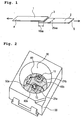
- FIG. 2 is a schematic perspective view illustrating one example of an optical semiconductor device
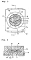
- FIG. 3 is a schematic plane view of the device
- FIG 4 is a schematic cross-sectional view along the line X-X of the optical semiconductor device illustrated in FIG. 3 .
- the optical semiconductor device comprises an optical semiconductor element 10, a package 20 inside which the optical semiconductor element 10 is mounted, and an encapsulating member 30 that covers the optical semiconductor element 10.
- the package 20 has conductive leads 21 (specifically, four leads 21 a, 21 b, 21 c and 21d).
- the package 20 has a cup-shaped depression having a bottom surface and a side surface, and the surfaces of the leads 21 are exposed at the bottom surface of the depression.
- the leads 21 are formed of silver or a silver-containing alloy or a base material such as iron or copper with a surface plated with silver.
- the optical semiconductor element 10 is connected to lead 21 a via a die bonding member 40 (not shown in Fig. 4 because of being a thin layer), is connected to another lead 21c via a wire 50a, and is connected to lead 21d via a wire 50b.
- a protective element 11 such as a zener may be mounted on another lead 21 b.
- the addition-curable silicone resin composition according to the present invention is used for the encapsulating member 30, and is injected into the interior of the cup-like shape of the package 20 and subsequently cured.
- the encapsulating member 30 may also contain a fluorescent material 60 that absorbs the light from the optical semiconductor element 10 and alters the wavelength of the light.
- optical semiconductor element examples include blue light-emitting LED chips formed from a gallium nitride (GaN) based semiconductor, and ultraviolet light-emitting LED chips and the like.
- GaN gallium nitride
- elements prepared by using a MOCVD method or the like to form a light emitting layer of a nitride semiconductor such as InN, AlN, InGaN, AlGaN or InGaAIN on top of a substrate may also be used. Either a face-up mounted optical semiconductor element or a flip-chip mounted optical semiconductor element may be used.
- optical semiconductor element illustrated in the drawings represents an example of an optical semiconductor element in which the n-side electrode and the p-side electrode are disposed on the same surface, but optical semiconductor elements in which the n-side electrode is provided on one surface and the p-side electrode is provided on the opposing surface can also be used.
- the pair of leads is integrally molded as part of the package, but different embodiments in which the package is first molded, and plating or the like is then used to provide circuit wiring on the package may also be used.
- the package may adopt any of a wide variety of shapes, including a flat plate-like shape or a cup-like shape.
- the package is provided with leads that supply an external electrical current to the optical semiconductor element, and is preferably formed from an electrically insulating material with excellent light resistance and heat resistance.
- the package material include thermoplastic resins such as polyphthalamide resins, thermosetting resins such as epoxy resins, as well as glass epoxy resins and ceramics.
- a white pigment such as titanium oxide may be mixed into the resin that constitutes the package.
- the leads that supply electrical power to the optical semiconductor element mounted on the bottom surface inside the cup-like shape can be formed comparatively easily by insert molding, injection molding, extrusion molding or transfer molding or the like.
- the leads are exposed at the bottom surface inside the cup-like shape of the package, are connected electrically to the optical semiconductor element, and, for example, may be plate-like leads that are inserted within the package, or a conductive pattern that is formed on the package surface.
- the leads may be formed of any material capable of performing the function of forming an electrical connection with the optical semiconductor element to achieve conduction, although forming the leads from a material having a comparatively high thermal conductivity is preferred.
- Specific examples of preferred materials include materials obtained by plating the surface of a metal such as copper, aluminum, gold, tungsten, iron or nickel, or an iron-nickel alloy, phosphor-bronze or iron-containing copper, with either silver or a silver-containing alloy. Elemental silver or alloys containing silver may also be used.
- the light reflection efficiency of the silver exposed at the surface of the leads deteriorates upon corrosion. Accordingly, the surfaces of the leads must be coated with a coating member to ensure that those portions that are irradiated either directly or indirectly with the light from the optical semiconductor element are able to maintain a high degree of reflectance.
- the encapsulating member has the functions of efficiently transmitting the light from the optical semiconductor element into the external environment, as well as protecting the optical semiconductor element and the wires and the like from external forces and dust and the like.
- the silicone resin according to the present invention is used as the encapsulating member.
- the encapsulating member may include a fluorescent material or a light diffusion member or the like.
- the fluorescent material which may be any material capable of absorbing the light emitted from the optical semiconductor element and converting the wavelength of the light to a different wavelength.
- the fluorescent material may be any material capable of absorbing the light emitted from the optical semiconductor element and converting the wavelength of the light to a different wavelength.
- fluorescent materials that may be used favorably include (Y,Gd) 3 (Al,Ga) 5 O 12 :Ce, (Ca,Sr,Ba) 2 SiO 4 :Eu, (Ca,Sr) 2 Si 5 N 8 :Eu and CaAlSiN 3 :Eu.
- compositions were evaluated using the methods described below.
- the curing conditions involved heating at 150°C for 4 hours.
- the results of the evaluations are listed in Table 1.
- a 1 mm thick cured product was prepared, and the external appearance was evaluated by visual inspection.
- a 1 mm thick cured product was prepared, and the light transmittance (%) of the product at 450 nm was measured using a spectrophotometer.
- An Abbe refractometer was used to measure the refractive index of the composition at 25°C relative to sodium-D light.
- the hardness was measured using a type-A spring tester, and the tensile strength and elongation were measured in accordance with JIS K 6301.
- two substrate pieces 1 and 2 formed from PPA (polyphthalamide resin) strips of width 25 mm were bonded together by overlapping the ends of the two pieces to a length of 10 mm with a 1 mm thick composition layer 3 provided between the overlapped ends, and then curing the composition layer 3 by heating for 4 hours at 150°C.
- the resulting specimen was left to stand at room temperature for at least 12 hours, and the tensile shear adhesive strength was then measured by using a tensile tester to pull the two ends 4 and 5 of the specimen in the directions indicated by the arrows.
- the fractured surface of the specimen following measurement of the shear adhesive strength in the manner described above was evaluated by determining the ratio of the surface area across which cohesive failure occurred (that is, those areas where the PPA substrate pieces and the cured product of the composition did not undergo interface separation, but rather the cured product itself fractured) relative to the total surface area of the fractured surface, and this ratio (as a percentage) was recorded as the cohesive failure rate.
- a commercially available top view light emitting device (NECW017 (product number), manufactured by Nichia Corporation) was used as an optical semiconductor device.
- This optical semiconductor device had a substantially cuboid shape with dimensions of length 3.5 mm x width 2.8 mm x height 2.0 mm.
- the package included a substantially circular cup-like shape with a diameter of approximately 2.5 mm in a plan view.
- 1,500 optical semiconductor devices were prepared. All 1,500 of these optical semiconductor devices were packed inside an aluminum bag of predetermined size, and left to stand for one month at ambient temperature.
- the devices were taken out of the bag, and the number of optical semiconductor devices in which the encapsulating member of one optical semiconductor device had adhered to the encapsulating member of another optical semiconductor device, in which detachment of the encapsulating member had occurred as a result of such adhesion, or in which some form of damage had occurred on the upper surface of the encapsulating member was counted.
- the results are detailed in Table 2.
- the cured product obtained from the composition of Comparative Example 3 in which the component (B2) was included in a larger amount than the component (B1), and the cured product obtained from the composition of Comparative Example 5 in which the component (A2) was included in a larger amount than the component (A1) exhibited poor heat resistance.
- composition of the present invention is useful as an encapsulant for all manner of optical semiconductor elements, including light receiving elements, photodiodes, phototransistors, optical sensors and laser diodes.
Landscapes
- Engineering & Computer Science (AREA)
- Chemical & Material Sciences (AREA)
- Microelectronics & Electronic Packaging (AREA)
- Power Engineering (AREA)
- Computer Hardware Design (AREA)
- Organic Chemistry (AREA)
- Health & Medical Sciences (AREA)
- Polymers & Plastics (AREA)
- Medicinal Chemistry (AREA)
- Chemical Kinetics & Catalysis (AREA)
- Manufacturing & Machinery (AREA)
- Physics & Mathematics (AREA)
- Materials Engineering (AREA)
- Condensed Matter Physics & Semiconductors (AREA)
- Electromagnetism (AREA)
- General Physics & Mathematics (AREA)
- Structures Or Materials For Encapsulating Or Coating Semiconductor Devices Or Solid State Devices (AREA)
- Compositions Of Macromolecular Compounds (AREA)
- Led Device Packages (AREA)
- Led Devices (AREA)
Claims (14)
- Zusammensetzung zur Einkapselung eines optischen Halbleiters, umfassend:(A) 100 Massenteile einer Organopolysiloxan-Komponente, die sich zusammensetzt aus einer Komponente (A1) und einer Komponente (A2), die unten beschrieben werden, wobei das Massenverhältnis der Komponente (A1)/Komponente (A2) in einem Bereich von 50/50 bis 95/5 liegt, und die Komponente (A) 0,005 bis 0,05 mol Alkenylgruppen pro 100g enthält und die Komponente (A) nicht mehr als 0,01 mol Silanolgruppen pro 100g enthält,(A1) ist ein Alkenylgruppen enthaltendes, lineares, Organopolysiloxan, repräsentiert durch die untenstehende Formel (1) und mit einer Viskosität bei 25°C zwischen 10 bis 1,000,000 mPa·s:
 (A2) ist ein Organopolysiloxan-Harz umfassend in jedem Molekül mindestens eine SiO2-Einheit und eine Alkenylgruppe,(B) ist eine Organohydrogenpolysiloxan-Komponente, die sich zusammensetzt aus einer Komponente (B1) und einer Komponente (B2), die unten beschrieben werden, wobei das molare Verhältnis von [SiH-Gruppen innerhalb der Komponente (B1)/ SiH-Gruppen innerhalb der Komponente (B2)] in einem Bereich von 50/50 bis 90/10 liegt, und eine Menge der Organohydrogenpolysiloxan-Komponente ergibt ein molares Verhältnis von [SiH-Gruppen innerhalb der Komponente (B)/Alkenylgruppen innerhalb der Komponente (A)] in einem Bereich von 0,9 bis 4,(B1) ist ein lineares Organohydrogenpolysiloxan mit zwei oder mehr SiH-Gruppen pro Molekül und repräsentiert durch die untenstehende Formel (2):
 (B2) ist ein verzweigtes Organohydrogenpolysiloxan, dass bei 25°C flüssig ist,(C) ist ein Katalysator auf Metallbasis aus der Platingruppe in einer wirksamen Menge, und(D) ist ein lineares oder zyklisches Organopolysiloxan aus 4 bis 50 Silikonatomen, welches mindestens über zwei funktionelle Gruppen, ausgewählt aus der Gruppe bestehend aus Silikonatom-gebundenen Alkenylgruppen, Alkosilylgruppen und Epoxygruppen, verfügt: in einer Menge in einem Bereich von 0,01 bis 10 Masseteilen pro 100 Masseteilen der Komponente (A).
 - Zusammensetzung nach Anspruch 1, wobei die Komponente (A) 0,007 bis 0,04 mol Alkenylgruppen pro 100g davon enthält.
- Zusammensetzung nach Anspruch 1, wobei das lineare Organoploysiloxan der Komponente (A1) Alkenylgruppen mit 2 bis 8 Kohlenstoffatomen an beiden terminalen Enden aufweist.
- Zusammensetzung nach Anspruch 1, wobei das lineare Organoploysiloxan der Komponente (A1) eine Viskosität bei 25°C zwischen 100 bis 100,000 mPa·s aufweist.
- Zusammensetzung nach Anspruch 1, wobei die Komponente (A2) SiO2-Einheiten in einer Menge von 1 mol% bis 70mol% bezogen auf die gesamten Siloxan-Einheiten der Komponente, enthält.
- Zusammensetzung nach Anspruch 1, wobei die Komponente (A2) mindestens zwei Alkenylgruppen pro Molekül enthält.
- Zusammensetzung nach Anspruch 1, wobei das Massenverhältnis der Komponente (A1)/Komponente (A2) in einem Bereich von 70/30 bis 90/10 liegt.
- Zusammensetzung nach Anspruch 1, wobei das molare Verhältnis der Alkenylgruppen innerhalb der Komponente (A1) zu Alkenylgruppen innerhalb der Komponente (A2) in einem Bereich von 1/2 bis 1/30 liegt.
- Zusammensetzung nach Anspruch 1, wobei das molare Verhältnis von [SiH-Gruppen innerhalb der Komponente (B)/Alkenylgruppen innerhalb der Komponente (A)] in einem Bereich von 1 bis 2 liegt.
- Zusammensetzung nach Anspruch 1, wobei das Organohydrogenpolysiloxan der Komponente (B1) mindestens zwei SiH-Gruppen pro Molekül enthält.
- Zusammensetzung nach Anspruch 1, wobei das Organohydrogenpolysiloxan der Komponente (B1) durch die Formel (2) repäsentiert wird:

- Zusammensetzung nach Anspruch 1, wobei das molare Verhältnis von [SiH-Gruppen innerhalb der Komponente (B1)/ SiH-Gruppen innerhalb der Komponente (B2)] in einem Bereich von 60/40 bis 80/20 liegt.
- Eine optische Halbleiter-Vorrichtung, umfassend ein optisches Halbleiterelement und eine Schicht gebildet durch ein gehärtetes Produkt einer Zusammensetzung wie in Anspruch 1 definiert, die das optische Halbleiterelement bedeckt.
- Eine optische Halbleiter-Vorrichtung gemäß Anspruch 13, wobei das optische Halbleiterelement eine Licht emittierende Diode ist.
Applications Claiming Priority (1)
| Application Number | Priority Date | Filing Date | Title |
|---|---|---|---|
| JP2009050737 | 2009-03-04 |
Publications (2)
| Publication Number | Publication Date |
|---|---|
| EP2226360A1 EP2226360A1 (de) | 2010-09-08 |
| EP2226360B1 true EP2226360B1 (de) | 2014-05-07 |
Family
ID=42313698
Family Applications (1)
| Application Number | Title | Priority Date | Filing Date |
|---|---|---|---|
| EP10002174.0A Active EP2226360B1 (de) | 2009-03-04 | 2010-03-03 | Zusammensetzung zur Einkapselung eines optischen Halbleiters und damit eingekapselte optische Halbleitervorrichtung |
Country Status (6)
| Country | Link |
|---|---|
| US (1) | US8373196B2 (de) |
| EP (1) | EP2226360B1 (de) |
| JP (1) | JP5499774B2 (de) |
| KR (1) | KR101660982B1 (de) |
| CN (1) | CN101824222B (de) |
| TW (1) | TWI448514B (de) |
Families Citing this family (44)
| Publication number | Priority date | Publication date | Assignee | Title |
|---|---|---|---|---|
| JP5549568B2 (ja) * | 2009-12-15 | 2014-07-16 | 信越化学工業株式会社 | 光半導体素子封止用樹脂組成物及び当該組成物で封止した光半導体装置 |
| JP5844252B2 (ja) * | 2010-04-02 | 2016-01-13 | 株式会社カネカ | 硬化性樹脂組成物、硬化性樹脂組成物タブレット、成形体、半導体のパッケージ、半導体部品及び発光ダイオード |
| CN103154144A (zh) * | 2010-10-14 | 2013-06-12 | 迈图高新材料日本合同公司 | 固化性聚有机硅氧烷组合物 |
| JP5490671B2 (ja) * | 2010-12-07 | 2014-05-14 | 信越化学工業株式会社 | シリコーン樹脂組成物の硬化方法 |
| WO2012086404A1 (ja) | 2010-12-22 | 2012-06-28 | モメンティブ・パフォーマンス・マテリアルズ・ジャパン合同会社 | 熱硬化型ポリオルガノシロキサン組成物及びその使用 |
| TWI435914B (zh) | 2010-12-31 | 2014-05-01 | Eternal Chemical Co Ltd | 可固化之有機聚矽氧烷組合物及其製法 |
| CN103619958B (zh) * | 2011-03-28 | 2016-06-29 | 汉高股份有限及两合公司 | 用于led封装的可固化的硅树脂 |
| CN102751420A (zh) * | 2011-04-19 | 2012-10-24 | 菱生精密工业股份有限公司 | 发光二极管封装结构 |
| JP5522116B2 (ja) * | 2011-04-28 | 2014-06-18 | 信越化学工業株式会社 | 付加硬化型シリコーン組成物及びそれを用いた光半導体装置 |
| JP5840388B2 (ja) * | 2011-06-01 | 2016-01-06 | 日東電工株式会社 | 発光ダイオード装置 |
| CN102408723A (zh) * | 2011-08-08 | 2012-04-11 | 吴世维 | 硅橡胶、硅橡胶制作方法及该硅橡胶制作的奶瓶 |
| JP6057503B2 (ja) * | 2011-09-21 | 2017-01-11 | 東レ・ダウコーニング株式会社 | 光半導体素子封止用硬化性シリコーン組成物、樹脂封止光半導体素子の製造方法、および樹脂封止光半導体素子 |
| JP5653877B2 (ja) * | 2011-10-04 | 2015-01-14 | 信越化学工業株式会社 | 光半導体封止用硬化性組成物及びこれを用いた光半導体装置 |
| CN103987788B (zh) | 2011-11-25 | 2017-06-09 | Lg化学株式会社 | 可固化组合物 |
| TWI473842B (zh) | 2011-11-25 | 2015-02-21 | Lg Chemical Ltd | 可固化之組成物 |
| KR101493131B1 (ko) * | 2011-11-25 | 2015-02-13 | 주식회사 엘지화학 | 오가노폴리실록산 |
| KR101562091B1 (ko) | 2011-11-25 | 2015-10-21 | 주식회사 엘지화학 | 경화성 조성물 |
| KR101453615B1 (ko) | 2011-11-25 | 2014-10-27 | 주식회사 엘지화학 | 경화성 조성물 |
| KR101409537B1 (ko) * | 2011-11-25 | 2014-06-19 | 주식회사 엘지화학 | 경화성 조성물 |
| TWI480316B (zh) * | 2012-07-13 | 2015-04-11 | Daxin Materials Corp | 含烯基或矽氫鍵的星狀聚矽氧烷以及熱硬化樹脂組成物 |
| KR101560044B1 (ko) | 2012-07-27 | 2015-10-15 | 주식회사 엘지화학 | 경화성 조성물 |
| JP5985981B2 (ja) * | 2012-12-28 | 2016-09-06 | 東レ・ダウコーニング株式会社 | 硬化性シリコーン組成物、その硬化物、および光半導体装置 |
| CN103408945B (zh) * | 2013-02-18 | 2016-01-20 | 永信新材料有限公司 | 可应用于发光二极管元件的聚硅氧烷组合物、基座配方及其发光二极管元件 |
| WO2014163438A1 (ko) * | 2013-04-04 | 2014-10-09 | 주식회사 엘지화학 | 경화성 조성물 |
| TWI490276B (zh) * | 2013-07-30 | 2015-07-01 | Chi Mei Corp | 矽樹脂封裝組成物及發光二極體裝置 |
| KR102185308B1 (ko) * | 2013-10-30 | 2020-12-01 | 신에쓰 가가꾸 고교 가부시끼가이샤 | 광 반도체 밀봉용 경화성 조성물 및 이것을 이용한 광 반도체 장치 |
| EP3153516A4 (de) | 2014-05-30 | 2018-03-07 | Dow Corning Toray Co., Ltd. | Organische siliciumverbindung, härtbare silikonzusammensetzung und halbleiterbauelement |
| CN105482429B (zh) * | 2014-10-01 | 2019-04-30 | 信越化学工业株式会社 | 光半导体密封用固化性组合物及使用此组合物的光半导体装置 |
| JP6276166B2 (ja) * | 2014-10-01 | 2018-02-07 | 信越化学工業株式会社 | 光半導体封止用硬化性組成物及びこれを用いた光半導体装置 |
| CN105713391B (zh) * | 2014-12-03 | 2018-11-09 | 广州慧谷化学有限公司 | 触变型有机聚硅氧烷组合物及半导体器件 |
| CN105985649B (zh) * | 2015-01-30 | 2019-03-19 | 广州慧谷化学有限公司 | 可固化的嵌段型有机聚硅氧烷组合物及半导体器件 |
| JP6389145B2 (ja) | 2015-06-05 | 2018-09-12 | 信越化学工業株式会社 | 付加硬化型シリコーン樹脂組成物、及び半導体装置 |
| JP6633859B2 (ja) * | 2015-07-31 | 2020-01-22 | ルネサスエレクトロニクス株式会社 | 半導体装置 |
| EP3420045A1 (de) * | 2016-02-23 | 2019-01-02 | Dow Silicones Corporation | Silikonkautschuk mit selektiver haftung |
| CN106010424A (zh) * | 2016-06-28 | 2016-10-12 | 华蓥市高科龙电子科技有限公司 | 一种发光二级管封装材料 |
| EP3770219A4 (de) * | 2018-03-20 | 2021-12-22 | Shin-Etsu Chemical Co., Ltd. | Silikongelzusammensetzung, gehärtetes produkt daraus und leistungsmodul |
| JP6969675B2 (ja) * | 2018-04-16 | 2021-11-24 | 信越化学工業株式会社 | 有機el用透明乾燥剤及びその使用方法 |
| US20220002594A1 (en) * | 2018-10-18 | 2022-01-06 | Dow Toray Co., Ltd. | Curable silicone composition and cured product thereof, layered product and production method therefor, and optical device or optical display |
| WO2020080349A1 (ja) * | 2018-10-18 | 2020-04-23 | ダウ・東レ株式会社 | 硬化性シリコーン組成物及びその硬化物、積層体及びその製造方法、並びに光学装置又は光学ディスプレイ |
| JP6966411B2 (ja) * | 2018-11-02 | 2021-11-17 | 信越化学工業株式会社 | 付加硬化型シリコーン樹脂組成物、その硬化物、及び光半導体装置 |
| CN111909517B (zh) * | 2019-05-10 | 2022-03-01 | 中国科学院化学研究所 | 一种可环线交联的有机硅组合物及反应产物及制备方法和应用 |
| JP7475135B2 (ja) * | 2019-12-25 | 2024-04-26 | デュポン・東レ・スペシャルティ・マテリアル株式会社 | 硬化性白色シリコーン組成物、光半導体装置用反射材、および光半導体装置 |
| KR102467690B1 (ko) * | 2020-08-19 | 2022-11-17 | 주식회사 케이씨씨실리콘 | 광학용 폴리실록산 조성물 및 이를 포함하는 광학 반도체용 반사 재료 |
| JP2023132309A (ja) | 2022-03-10 | 2023-09-22 | デュポン・東レ・スペシャルティ・マテリアル株式会社 | 硬化性シリコーン組成物 |
Family Cites Families (21)
| Publication number | Priority date | Publication date | Assignee | Title |
|---|---|---|---|---|
| US3996195A (en) * | 1974-11-15 | 1976-12-07 | Shinetsu Chemical Company | Curable organosilicon compositions |
| JPS5239751A (en) * | 1975-09-26 | 1977-03-28 | Shin Etsu Chem Co Ltd | Curable organopolysiloxane compositions |
| US4427801A (en) * | 1982-04-14 | 1984-01-24 | Dow Corning Corporation | Extrudable silicone elastomer compositions |
| JPS6183251A (ja) * | 1984-10-01 | 1986-04-26 | Shin Etsu Chem Co Ltd | 硬化性オルガノポリシロキサン組成物 |
| US5082886A (en) * | 1989-08-28 | 1992-01-21 | General Electric Company | Low compression set, oil and fuel resistant, liquid injection moldable, silicone rubber |
| US5198479A (en) * | 1990-08-24 | 1993-03-30 | Shin-Etsu Chemical Company Limited | Light transmissive epoxy resin compositions and optical semiconductor devices encapsulated therewith |
| US6124407A (en) * | 1998-10-28 | 2000-09-26 | Dow Corning Corporation | Silicone composition, method for the preparation thereof, and silicone elastomer |
| JP3523098B2 (ja) * | 1998-12-28 | 2004-04-26 | 信越化学工業株式会社 | 付加硬化型シリコーン組成物 |
| JP3865639B2 (ja) * | 2002-01-28 | 2007-01-10 | 信越化学工業株式会社 | 半導体封止用シリコーン組成物および半導体装置 |
| JP4409160B2 (ja) * | 2002-10-28 | 2010-02-03 | 東レ・ダウコーニング株式会社 | 硬化性オルガノポリシロキサン組成物および半導体装置 |
| JP4154605B2 (ja) * | 2004-01-23 | 2008-09-24 | 信越化学工業株式会社 | 熱伝導性シリコーン放熱用組成物及び放熱構造の製造方法 |
| JP4300418B2 (ja) * | 2004-04-30 | 2009-07-22 | 信越化学工業株式会社 | エポキシ・シリコーン混成樹脂組成物及び発光半導体装置 |
| JP4455218B2 (ja) * | 2004-08-12 | 2010-04-21 | 信越化学工業株式会社 | 自己接着性付加反応硬化型シリコーン組成物 |
| JP4623282B2 (ja) * | 2005-03-10 | 2011-02-02 | 信越化学工業株式会社 | 半導体装置の製造方法 |
| US7588967B2 (en) * | 2005-05-27 | 2009-09-15 | Shin-Etsu Chemical Co., Ltd. | Curable silicone rubber composition and semiconductor device |
| JP2007063538A (ja) * | 2005-08-03 | 2007-03-15 | Shin Etsu Chem Co Ltd | 発光ダイオード用付加硬化型シリコーン樹脂組成物 |
| JP4872296B2 (ja) | 2005-09-30 | 2012-02-08 | 日亜化学工業株式会社 | シリコーンゴム封止型発光装置、及び該発光装置の製造方法 |
| JP4684835B2 (ja) * | 2005-09-30 | 2011-05-18 | 信越化学工業株式会社 | シリコーンゴム硬化物の表面タック性を低減する方法、半導体封止用液状シリコーンゴム組成物、シリコーンゴム封止型半導体装置、及び該半導体装置の製造方法 |
| US7479522B2 (en) * | 2005-11-09 | 2009-01-20 | Momentive Performance Materials Inc. | Silicone elastomer composition |
| TWI434890B (zh) * | 2007-04-06 | 2014-04-21 | Shinetsu Chemical Co | 加成可硬化聚矽氧樹脂組成物及使用彼之聚矽氧鏡片 |
| JP5526823B2 (ja) * | 2009-02-24 | 2014-06-18 | 信越化学工業株式会社 | シリコーン樹脂で封止された光半導体装置 |
-
2010
- 2010-03-02 JP JP2010044910A patent/JP5499774B2/ja active Active
- 2010-03-03 US US12/716,823 patent/US8373196B2/en active Active
- 2010-03-03 KR KR1020100018794A patent/KR101660982B1/ko active IP Right Grant
- 2010-03-03 EP EP10002174.0A patent/EP2226360B1/de active Active
- 2010-03-03 TW TW099106113A patent/TWI448514B/zh active
- 2010-03-04 CN CN2010101298630A patent/CN101824222B/zh active Active
Also Published As
| Publication number | Publication date |
|---|---|
| CN101824222A (zh) | 2010-09-08 |
| EP2226360A1 (de) | 2010-09-08 |
| KR101660982B1 (ko) | 2016-09-28 |
| US20100224906A1 (en) | 2010-09-09 |
| JP5499774B2 (ja) | 2014-05-21 |
| KR20100100634A (ko) | 2010-09-15 |
| CN101824222B (zh) | 2012-08-29 |
| US8373196B2 (en) | 2013-02-12 |
| TWI448514B (zh) | 2014-08-11 |
| TW201040229A (en) | 2010-11-16 |
| JP2010229402A (ja) | 2010-10-14 |
Similar Documents
| Publication | Publication Date | Title |
|---|---|---|
| EP2226360B1 (de) | Zusammensetzung zur Einkapselung eines optischen Halbleiters und damit eingekapselte optische Halbleitervorrichtung | |
| EP2221868B1 (de) | Optisches Halbleiterbauelement, das mit Silikonharz eingekapselt ist | |
| CN105121556B (zh) | 可固化有机硅组合物、其固化产物及光学半导体器件 | |
| EP2105466B1 (de) | Härtbare Silikon-Kautschuk-Zusammensetzung und Halbleitervorrichtungen | |
| EP2588538B1 (de) | Härtbare organopolysiloxanzusammensetzung und optisches halbleiterbauelement | |
| US9012586B2 (en) | Curable organopolysiloxane composition and optical semiconductor device | |
| CN109890899B (zh) | 固化性有机硅组合物、其固化物、及光半导体装置 | |
| KR20150050401A (ko) | 광 반도체 밀봉용 경화성 조성물 및 이것을 이용한 광 반도체 장치 | |
| CN110382625B (zh) | 可固化的有机聚硅氧烷组合物和半导体器件 | |
| KR20200108047A (ko) | 경화성 실리콘 조성물, 이의 경화물, 및 광반도체 장치 | |
| KR20200037261A (ko) | 경화성 유기폴리실록산 조성물 및 광반도체 장치 | |
| KR102339576B1 (ko) | 광반도체 봉지용 경화성 조성물 및 이를 이용한 광반도체 장치 | |
| KR20220094127A (ko) | 경화성 실리콘 조성물, 봉지재, 및 광 반도체 장치 |
Legal Events
| Date | Code | Title | Description |
|---|---|---|---|
| PUAI | Public reference made under article 153(3) epc to a published international application that has entered the european phase |
Free format text: ORIGINAL CODE: 0009012 |
|
| AK | Designated contracting states |
Kind code of ref document: A1 Designated state(s): AT BE BG CH CY CZ DE DK EE ES FI FR GB GR HR HU IE IS IT LI LT LU LV MC MK MT NL NO PL PT RO SE SI SK SM TR |
|
| AX | Request for extension of the european patent |
Extension state: AL BA ME RS |
|
| 17P | Request for examination filed |
Effective date: 20110302 |
|
| GRAP | Despatch of communication of intention to grant a patent |
Free format text: ORIGINAL CODE: EPIDOSNIGR1 |
|
| RAP1 | Party data changed (applicant data changed or rights of an application transferred) |
Owner name: SHIN-ETSU CHEMICAL CO., LTD. |
|
| INTG | Intention to grant announced |
Effective date: 20140102 |
|
| GRAS | Grant fee paid |
Free format text: ORIGINAL CODE: EPIDOSNIGR3 |
|
| GRAA | (expected) grant |
Free format text: ORIGINAL CODE: 0009210 |
|
| AK | Designated contracting states |
Kind code of ref document: B1 Designated state(s): AT BE BG CH CY CZ DE DK EE ES FI FR GB GR HR HU IE IS IT LI LT LU LV MC MK MT NL NO PL PT RO SE SI SK SM TR |
|
| REG | Reference to a national code |
Ref country code: GB Ref legal event code: FG4D |
|
| REG | Reference to a national code |
Ref country code: AT Ref legal event code: REF Ref document number: 666681 Country of ref document: AT Kind code of ref document: T Effective date: 20140515 |
|
| REG | Reference to a national code |
Ref country code: IE Ref legal event code: FG4D |
|
| REG | Reference to a national code |
Ref country code: DE Ref legal event code: R096 Ref document number: 602010015737 Country of ref document: DE Effective date: 20140618 |
|
| REG | Reference to a national code |
Ref country code: AT Ref legal event code: MK05 Ref document number: 666681 Country of ref document: AT Kind code of ref document: T Effective date: 20140507 |
|
| REG | Reference to a national code |
Ref country code: NL Ref legal event code: VDEP Effective date: 20140507 |
|
| REG | Reference to a national code |
Ref country code: LT Ref legal event code: MG4D |
|
| PG25 | Lapsed in a contracting state [announced via postgrant information from national office to epo] |
Ref country code: FI Free format text: LAPSE BECAUSE OF FAILURE TO SUBMIT A TRANSLATION OF THE DESCRIPTION OR TO PAY THE FEE WITHIN THE PRESCRIBED TIME-LIMIT Effective date: 20140507 Ref country code: IS Free format text: LAPSE BECAUSE OF FAILURE TO SUBMIT A TRANSLATION OF THE DESCRIPTION OR TO PAY THE FEE WITHIN THE PRESCRIBED TIME-LIMIT Effective date: 20140907 Ref country code: LT Free format text: LAPSE BECAUSE OF FAILURE TO SUBMIT A TRANSLATION OF THE DESCRIPTION OR TO PAY THE FEE WITHIN THE PRESCRIBED TIME-LIMIT Effective date: 20140507 Ref country code: NO Free format text: LAPSE BECAUSE OF FAILURE TO SUBMIT A TRANSLATION OF THE DESCRIPTION OR TO PAY THE FEE WITHIN THE PRESCRIBED TIME-LIMIT Effective date: 20140807 Ref country code: CY Free format text: LAPSE BECAUSE OF FAILURE TO SUBMIT A TRANSLATION OF THE DESCRIPTION OR TO PAY THE FEE WITHIN THE PRESCRIBED TIME-LIMIT Effective date: 20140507 Ref country code: GR Free format text: LAPSE BECAUSE OF FAILURE TO SUBMIT A TRANSLATION OF THE DESCRIPTION OR TO PAY THE FEE WITHIN THE PRESCRIBED TIME-LIMIT Effective date: 20140808 |
|
| PG25 | Lapsed in a contracting state [announced via postgrant information from national office to epo] |
Ref country code: PL Free format text: LAPSE BECAUSE OF FAILURE TO SUBMIT A TRANSLATION OF THE DESCRIPTION OR TO PAY THE FEE WITHIN THE PRESCRIBED TIME-LIMIT Effective date: 20140507 Ref country code: ES Free format text: LAPSE BECAUSE OF FAILURE TO SUBMIT A TRANSLATION OF THE DESCRIPTION OR TO PAY THE FEE WITHIN THE PRESCRIBED TIME-LIMIT Effective date: 20140507 Ref country code: SE Free format text: LAPSE BECAUSE OF FAILURE TO SUBMIT A TRANSLATION OF THE DESCRIPTION OR TO PAY THE FEE WITHIN THE PRESCRIBED TIME-LIMIT Effective date: 20140507 Ref country code: AT Free format text: LAPSE BECAUSE OF FAILURE TO SUBMIT A TRANSLATION OF THE DESCRIPTION OR TO PAY THE FEE WITHIN THE PRESCRIBED TIME-LIMIT Effective date: 20140507 Ref country code: LV Free format text: LAPSE BECAUSE OF FAILURE TO SUBMIT A TRANSLATION OF THE DESCRIPTION OR TO PAY THE FEE WITHIN THE PRESCRIBED TIME-LIMIT Effective date: 20140507 Ref country code: HR Free format text: LAPSE BECAUSE OF FAILURE TO SUBMIT A TRANSLATION OF THE DESCRIPTION OR TO PAY THE FEE WITHIN THE PRESCRIBED TIME-LIMIT Effective date: 20140507 |
|
| PG25 | Lapsed in a contracting state [announced via postgrant information from national office to epo] |
Ref country code: PT Free format text: LAPSE BECAUSE OF FAILURE TO SUBMIT A TRANSLATION OF THE DESCRIPTION OR TO PAY THE FEE WITHIN THE PRESCRIBED TIME-LIMIT Effective date: 20140908 |
|
| PG25 | Lapsed in a contracting state [announced via postgrant information from national office to epo] |
Ref country code: RO Free format text: LAPSE BECAUSE OF FAILURE TO SUBMIT A TRANSLATION OF THE DESCRIPTION OR TO PAY THE FEE WITHIN THE PRESCRIBED TIME-LIMIT Effective date: 20140507 Ref country code: CZ Free format text: LAPSE BECAUSE OF FAILURE TO SUBMIT A TRANSLATION OF THE DESCRIPTION OR TO PAY THE FEE WITHIN THE PRESCRIBED TIME-LIMIT Effective date: 20140507 Ref country code: SK Free format text: LAPSE BECAUSE OF FAILURE TO SUBMIT A TRANSLATION OF THE DESCRIPTION OR TO PAY THE FEE WITHIN THE PRESCRIBED TIME-LIMIT Effective date: 20140507 Ref country code: EE Free format text: LAPSE BECAUSE OF FAILURE TO SUBMIT A TRANSLATION OF THE DESCRIPTION OR TO PAY THE FEE WITHIN THE PRESCRIBED TIME-LIMIT Effective date: 20140507 Ref country code: BE Free format text: LAPSE BECAUSE OF FAILURE TO SUBMIT A TRANSLATION OF THE DESCRIPTION OR TO PAY THE FEE WITHIN THE PRESCRIBED TIME-LIMIT Effective date: 20140507 Ref country code: DK Free format text: LAPSE BECAUSE OF FAILURE TO SUBMIT A TRANSLATION OF THE DESCRIPTION OR TO PAY THE FEE WITHIN THE PRESCRIBED TIME-LIMIT Effective date: 20140507 |
|
| REG | Reference to a national code |
Ref country code: DE Ref legal event code: R097 Ref document number: 602010015737 Country of ref document: DE |
|
| PG25 | Lapsed in a contracting state [announced via postgrant information from national office to epo] |
Ref country code: NL Free format text: LAPSE BECAUSE OF FAILURE TO SUBMIT A TRANSLATION OF THE DESCRIPTION OR TO PAY THE FEE WITHIN THE PRESCRIBED TIME-LIMIT Effective date: 20140507 |
|
| PLBE | No opposition filed within time limit |
Free format text: ORIGINAL CODE: 0009261 |
|
| STAA | Information on the status of an ep patent application or granted ep patent |
Free format text: STATUS: NO OPPOSITION FILED WITHIN TIME LIMIT |
|
| 26N | No opposition filed |
Effective date: 20150210 |
|
| PG25 | Lapsed in a contracting state [announced via postgrant information from national office to epo] |
Ref country code: IT Free format text: LAPSE BECAUSE OF FAILURE TO SUBMIT A TRANSLATION OF THE DESCRIPTION OR TO PAY THE FEE WITHIN THE PRESCRIBED TIME-LIMIT Effective date: 20140507 |
|
| REG | Reference to a national code |
Ref country code: DE Ref legal event code: R097 Ref document number: 602010015737 Country of ref document: DE Effective date: 20150210 |
|
| PG25 | Lapsed in a contracting state [announced via postgrant information from national office to epo] |
Ref country code: SI Free format text: LAPSE BECAUSE OF FAILURE TO SUBMIT A TRANSLATION OF THE DESCRIPTION OR TO PAY THE FEE WITHIN THE PRESCRIBED TIME-LIMIT Effective date: 20140507 |
|
| PG25 | Lapsed in a contracting state [announced via postgrant information from national office to epo] |
Ref country code: LU Free format text: LAPSE BECAUSE OF FAILURE TO SUBMIT A TRANSLATION OF THE DESCRIPTION OR TO PAY THE FEE WITHIN THE PRESCRIBED TIME-LIMIT Effective date: 20150303 Ref country code: MC Free format text: LAPSE BECAUSE OF FAILURE TO SUBMIT A TRANSLATION OF THE DESCRIPTION OR TO PAY THE FEE WITHIN THE PRESCRIBED TIME-LIMIT Effective date: 20140507 |
|
| REG | Reference to a national code |
Ref country code: CH Ref legal event code: PL |
|
| GBPC | Gb: european patent ceased through non-payment of renewal fee |
Effective date: 20150303 |
|
| REG | Reference to a national code |
Ref country code: FR Ref legal event code: ST Effective date: 20151130 |
|
| REG | Reference to a national code |
Ref country code: IE Ref legal event code: MM4A |
|
| PG25 | Lapsed in a contracting state [announced via postgrant information from national office to epo] |
Ref country code: LI Free format text: LAPSE BECAUSE OF NON-PAYMENT OF DUE FEES Effective date: 20150331 Ref country code: CH Free format text: LAPSE BECAUSE OF NON-PAYMENT OF DUE FEES Effective date: 20150331 Ref country code: GB Free format text: LAPSE BECAUSE OF NON-PAYMENT OF DUE FEES Effective date: 20150303 Ref country code: IE Free format text: LAPSE BECAUSE OF NON-PAYMENT OF DUE FEES Effective date: 20150303 |
|
| PG25 | Lapsed in a contracting state [announced via postgrant information from national office to epo] |
Ref country code: FR Free format text: LAPSE BECAUSE OF NON-PAYMENT OF DUE FEES Effective date: 20150331 |
|
| PG25 | Lapsed in a contracting state [announced via postgrant information from national office to epo] |
Ref country code: MT Free format text: LAPSE BECAUSE OF FAILURE TO SUBMIT A TRANSLATION OF THE DESCRIPTION OR TO PAY THE FEE WITHIN THE PRESCRIBED TIME-LIMIT Effective date: 20140507 |
|
| PG25 | Lapsed in a contracting state [announced via postgrant information from national office to epo] |
Ref country code: HU Free format text: LAPSE BECAUSE OF FAILURE TO SUBMIT A TRANSLATION OF THE DESCRIPTION OR TO PAY THE FEE WITHIN THE PRESCRIBED TIME-LIMIT; INVALID AB INITIO Effective date: 20100303 Ref country code: BG Free format text: LAPSE BECAUSE OF FAILURE TO SUBMIT A TRANSLATION OF THE DESCRIPTION OR TO PAY THE FEE WITHIN THE PRESCRIBED TIME-LIMIT Effective date: 20140507 Ref country code: SM Free format text: LAPSE BECAUSE OF FAILURE TO SUBMIT A TRANSLATION OF THE DESCRIPTION OR TO PAY THE FEE WITHIN THE PRESCRIBED TIME-LIMIT Effective date: 20140507 |
|
| PG25 | Lapsed in a contracting state [announced via postgrant information from national office to epo] |
Ref country code: TR Free format text: LAPSE BECAUSE OF FAILURE TO SUBMIT A TRANSLATION OF THE DESCRIPTION OR TO PAY THE FEE WITHIN THE PRESCRIBED TIME-LIMIT Effective date: 20140507 |
|
| PG25 | Lapsed in a contracting state [announced via postgrant information from national office to epo] |
Ref country code: MK Free format text: LAPSE BECAUSE OF FAILURE TO SUBMIT A TRANSLATION OF THE DESCRIPTION OR TO PAY THE FEE WITHIN THE PRESCRIBED TIME-LIMIT Effective date: 20140507 |
|
| REG | Reference to a national code |
Ref country code: DE Ref legal event code: R082 Ref document number: 602010015737 Country of ref document: DE Representative=s name: ZACCO LEGAL RECHTSANWALTSGESELLSCHAFT MBH, DE |
|
| PGFP | Annual fee paid to national office [announced via postgrant information from national office to epo] |
Ref country code: DE Payment date: 20240130 Year of fee payment: 15 |