EP2216680B1 - Feinteilchen und Herstellungsverfahren dafür - Google Patents
Feinteilchen und Herstellungsverfahren dafür Download PDFInfo
- Publication number
- EP2216680B1 EP2216680B1 EP10000365.6A EP10000365A EP2216680B1 EP 2216680 B1 EP2216680 B1 EP 2216680B1 EP 10000365 A EP10000365 A EP 10000365A EP 2216680 B1 EP2216680 B1 EP 2216680B1
- Authority
- EP
- European Patent Office
- Prior art keywords
- concavo
- fine particles
- convex pattern
- vapor deposition
- base material
- Prior art date
- Legal status (The legal status is an assumption and is not a legal conclusion. Google has not performed a legal analysis and makes no representation as to the accuracy of the status listed.)
- Not-in-force
Links
- 239000010419 fine particle Substances 0.000 title claims description 167
- 238000004519 manufacturing process Methods 0.000 title claims description 8
- 239000000463 material Substances 0.000 claims description 80
- 238000000034 method Methods 0.000 claims description 71
- 239000012044 organic layer Substances 0.000 claims description 66
- 238000007740 vapor deposition Methods 0.000 claims description 48
- 239000010410 layer Substances 0.000 claims description 38
- 239000002904 solvent Substances 0.000 claims description 21
- 230000008859 change Effects 0.000 claims description 13
- 239000000203 mixture Substances 0.000 claims description 8
- 238000000926 separation method Methods 0.000 claims description 7
- 238000005530 etching Methods 0.000 claims description 4
- 239000000049 pigment Substances 0.000 description 66
- 239000000758 substrate Substances 0.000 description 30
- 229910052782 aluminium Inorganic materials 0.000 description 23
- 239000002245 particle Substances 0.000 description 22
- XAGFODPZIPBFFR-UHFFFAOYSA-N aluminium Chemical compound [Al] XAGFODPZIPBFFR-UHFFFAOYSA-N 0.000 description 21
- 238000000576 coating method Methods 0.000 description 19
- 239000000126 substance Substances 0.000 description 18
- 239000011248 coating agent Substances 0.000 description 17
- 238000000151 deposition Methods 0.000 description 16
- 150000001875 compounds Chemical class 0.000 description 14
- 230000008021 deposition Effects 0.000 description 13
- 230000015572 biosynthetic process Effects 0.000 description 11
- 239000011521 glass Substances 0.000 description 10
- 230000003287 optical effect Effects 0.000 description 10
- NBUKAOOFKZFCGD-UHFFFAOYSA-N 2,2,3,3-tetrafluoropropan-1-ol Chemical compound OCC(F)(F)C(F)F NBUKAOOFKZFCGD-UHFFFAOYSA-N 0.000 description 9
- XUIMIQQOPSSXEZ-UHFFFAOYSA-N Silicon Chemical compound [Si] XUIMIQQOPSSXEZ-UHFFFAOYSA-N 0.000 description 9
- 239000010408 film Substances 0.000 description 9
- 230000010355 oscillation Effects 0.000 description 9
- 239000010703 silicon Substances 0.000 description 9
- 229910052710 silicon Inorganic materials 0.000 description 9
- 238000001312 dry etching Methods 0.000 description 7
- 239000011859 microparticle Substances 0.000 description 7
- 239000011347 resin Substances 0.000 description 7
- 229920005989 resin Polymers 0.000 description 7
- ZWEHNKRNPOVVGH-UHFFFAOYSA-N 2-Butanone Chemical compound CCC(C)=O ZWEHNKRNPOVVGH-UHFFFAOYSA-N 0.000 description 6
- BQCADISMDOOEFD-UHFFFAOYSA-N Silver Chemical compound [Ag] BQCADISMDOOEFD-UHFFFAOYSA-N 0.000 description 6
- 239000007767 bonding agent Substances 0.000 description 6
- 230000001965 increasing effect Effects 0.000 description 6
- -1 polyethylene terephthalate Polymers 0.000 description 6
- 229910052709 silver Inorganic materials 0.000 description 6
- 239000004332 silver Substances 0.000 description 6
- 238000000354 decomposition reaction Methods 0.000 description 5
- 229910052751 metal Inorganic materials 0.000 description 5
- 239000002184 metal Substances 0.000 description 5
- IEQIEDJGQAUEQZ-UHFFFAOYSA-N phthalocyanine Chemical compound N1C(N=C2C3=CC=CC=C3C(N=C3C4=CC=CC=C4C(=N4)N3)=N2)=C(C=CC=C2)C2=C1N=C1C2=CC=CC=C2C4=N1 IEQIEDJGQAUEQZ-UHFFFAOYSA-N 0.000 description 5
- 229920003229 poly(methyl methacrylate) Polymers 0.000 description 5
- 239000004926 polymethyl methacrylate Substances 0.000 description 5
- 238000004528 spin coating Methods 0.000 description 5
- 238000000859 sublimation Methods 0.000 description 5
- 230000008022 sublimation Effects 0.000 description 5
- ANRHNWWPFJCPAZ-UHFFFAOYSA-M thionine Chemical compound [Cl-].C1=CC(N)=CC2=[S+]C3=CC(N)=CC=C3N=C21 ANRHNWWPFJCPAZ-UHFFFAOYSA-M 0.000 description 5
- 238000009834 vaporization Methods 0.000 description 5
- 230000008016 vaporization Effects 0.000 description 5
- KFZMGEQAYNKOFK-UHFFFAOYSA-N Isopropanol Chemical compound CC(C)O KFZMGEQAYNKOFK-UHFFFAOYSA-N 0.000 description 4
- VYPSYNLAJGMNEJ-UHFFFAOYSA-N Silicium dioxide Chemical compound O=[Si]=O VYPSYNLAJGMNEJ-UHFFFAOYSA-N 0.000 description 4
- 239000011230 binding agent Substances 0.000 description 4
- 239000003795 chemical substances by application Substances 0.000 description 4
- ZYGHJZDHTFUPRJ-UHFFFAOYSA-N coumarin Chemical compound C1=CC=C2OC(=O)C=CC2=C1 ZYGHJZDHTFUPRJ-UHFFFAOYSA-N 0.000 description 4
- 230000007423 decrease Effects 0.000 description 4
- 238000002845 discoloration Methods 0.000 description 4
- LZCLXQDLBQLTDK-UHFFFAOYSA-N ethyl 2-hydroxypropanoate Chemical compound CCOC(=O)C(C)O LZCLXQDLBQLTDK-UHFFFAOYSA-N 0.000 description 4
- 230000009477 glass transition Effects 0.000 description 4
- 229910052737 gold Inorganic materials 0.000 description 4
- 239000010931 gold Substances 0.000 description 4
- 150000002739 metals Chemical class 0.000 description 4
- 239000005020 polyethylene terephthalate Substances 0.000 description 4
- 229920000139 polyethylene terephthalate Polymers 0.000 description 4
- 230000009467 reduction Effects 0.000 description 4
- 238000004544 sputter deposition Methods 0.000 description 4
- 239000010409 thin film Substances 0.000 description 4
- 230000007704 transition Effects 0.000 description 4
- YMWUJEATGCHHMB-UHFFFAOYSA-N Dichloromethane Chemical compound ClCCl YMWUJEATGCHHMB-UHFFFAOYSA-N 0.000 description 3
- MYMOFIZGZYHOMD-UHFFFAOYSA-N Dioxygen Chemical compound O=O MYMOFIZGZYHOMD-UHFFFAOYSA-N 0.000 description 3
- LFQSCWFLJHTTHZ-UHFFFAOYSA-N Ethanol Chemical compound CCO LFQSCWFLJHTTHZ-UHFFFAOYSA-N 0.000 description 3
- YCKRFDGAMUMZLT-UHFFFAOYSA-N Fluorine atom Chemical compound [F] YCKRFDGAMUMZLT-UHFFFAOYSA-N 0.000 description 3
- ZMXDDKWLCZADIW-UHFFFAOYSA-N N,N-Dimethylformamide Chemical compound CN(C)C=O ZMXDDKWLCZADIW-UHFFFAOYSA-N 0.000 description 3
- 238000006243 chemical reaction Methods 0.000 description 3
- 229910052731 fluorine Inorganic materials 0.000 description 3
- 239000011737 fluorine Substances 0.000 description 3
- DZVCFNFOPIZQKX-LTHRDKTGSA-M merocyanine Chemical compound [Na+].O=C1N(CCCC)C(=O)N(CCCC)C(=O)C1=C\C=C\C=C/1N(CCCS([O-])(=O)=O)C2=CC=CC=C2O\1 DZVCFNFOPIZQKX-LTHRDKTGSA-M 0.000 description 3
- 239000004417 polycarbonate Substances 0.000 description 3
- 229920000515 polycarbonate Polymers 0.000 description 3
- 230000008569 process Effects 0.000 description 3
- 239000004065 semiconductor Substances 0.000 description 3
- 238000005507 spraying Methods 0.000 description 3
- AZQWKYJCGOJGHM-UHFFFAOYSA-N 1,4-benzoquinone Chemical compound O=C1C=CC(=O)C=C1 AZQWKYJCGOJGHM-UHFFFAOYSA-N 0.000 description 2
- SVONRAPFKPVNKG-UHFFFAOYSA-N 2-ethoxyethyl acetate Chemical compound CCOCCOC(C)=O SVONRAPFKPVNKG-UHFFFAOYSA-N 0.000 description 2
- CSCPPACGZOOCGX-UHFFFAOYSA-N Acetone Chemical compound CC(C)=O CSCPPACGZOOCGX-UHFFFAOYSA-N 0.000 description 2
- DKPFZGUDAPQIHT-UHFFFAOYSA-N Butyl acetate Natural products CCCCOC(C)=O DKPFZGUDAPQIHT-UHFFFAOYSA-N 0.000 description 2
- HEDRZPFGACZZDS-UHFFFAOYSA-N Chloroform Chemical compound ClC(Cl)Cl HEDRZPFGACZZDS-UHFFFAOYSA-N 0.000 description 2
- RTZKZFJDLAIYFH-UHFFFAOYSA-N Diethyl ether Chemical compound CCOCC RTZKZFJDLAIYFH-UHFFFAOYSA-N 0.000 description 2
- WYURNTSHIVDZCO-UHFFFAOYSA-N Tetrahydrofuran Chemical compound C1CCOC1 WYURNTSHIVDZCO-UHFFFAOYSA-N 0.000 description 2
- 238000010521 absorption reaction Methods 0.000 description 2
- 239000000956 alloy Substances 0.000 description 2
- 229910045601 alloy Inorganic materials 0.000 description 2
- 125000002820 allylidene group Chemical group [H]C(=[*])C([H])=C([H])[H] 0.000 description 2
- 150000007980 azole derivatives Chemical class 0.000 description 2
- BUNYBPVXEKRSGY-UHFFFAOYSA-N buta-1,3-dien-1-amine Chemical class NC=CC=C BUNYBPVXEKRSGY-UHFFFAOYSA-N 0.000 description 2
- 239000001913 cellulose Substances 0.000 description 2
- 229920002678 cellulose Polymers 0.000 description 2
- 229910052804 chromium Inorganic materials 0.000 description 2
- 229910052802 copper Inorganic materials 0.000 description 2
- 235000001671 coumarin Nutrition 0.000 description 2
- 229960000956 coumarin Drugs 0.000 description 2
- JHIVVAPYMSGYDF-UHFFFAOYSA-N cyclohexanone Chemical compound O=C1CCCCC1 JHIVVAPYMSGYDF-UHFFFAOYSA-N 0.000 description 2
- 230000003247 decreasing effect Effects 0.000 description 2
- 238000009826 distribution Methods 0.000 description 2
- 229920001971 elastomer Polymers 0.000 description 2
- 230000002708 enhancing effect Effects 0.000 description 2
- 229940116333 ethyl lactate Drugs 0.000 description 2
- 239000007789 gas Substances 0.000 description 2
- PCHJSUWPFVWCPO-UHFFFAOYSA-N gold Chemical compound [Au] PCHJSUWPFVWCPO-UHFFFAOYSA-N 0.000 description 2
- 238000010438 heat treatment Methods 0.000 description 2
- FUZZWVXGSFPDMH-UHFFFAOYSA-N hexanoic acid Chemical compound CCCCCC(O)=O FUZZWVXGSFPDMH-UHFFFAOYSA-N 0.000 description 2
- 229930195733 hydrocarbon Natural products 0.000 description 2
- 150000002430 hydrocarbons Chemical class 0.000 description 2
- 239000007791 liquid phase Substances 0.000 description 2
- 125000001434 methanylylidene group Chemical group [H]C#[*] 0.000 description 2
- UAEPNZWRGJTJPN-UHFFFAOYSA-N methylcyclohexane Chemical compound CC1CCCCC1 UAEPNZWRGJTJPN-UHFFFAOYSA-N 0.000 description 2
- 229910052750 molybdenum Inorganic materials 0.000 description 2
- 238000000465 moulding Methods 0.000 description 2
- LKKPNUDVOYAOBB-UHFFFAOYSA-N naphthalocyanine Chemical compound N1C(N=C2C3=CC4=CC=CC=C4C=C3C(N=C3C4=CC5=CC=CC=C5C=C4C(=N4)N3)=N2)=C(C=C2C(C=CC=C2)=C2)C2=C1N=C1C2=CC3=CC=CC=C3C=C2C4=N1 LKKPNUDVOYAOBB-UHFFFAOYSA-N 0.000 description 2
- 229910052759 nickel Inorganic materials 0.000 description 2
- 229920002120 photoresistant polymer Polymers 0.000 description 2
- 238000001020 plasma etching Methods 0.000 description 2
- 229910052697 platinum Inorganic materials 0.000 description 2
- BASFCYQUMIYNBI-UHFFFAOYSA-N platinum Substances [Pt] BASFCYQUMIYNBI-UHFFFAOYSA-N 0.000 description 2
- 239000011112 polyethylene naphthalate Substances 0.000 description 2
- 150000004032 porphyrins Chemical class 0.000 description 2
- BDERNNFJNOPAEC-UHFFFAOYSA-N propan-1-ol Chemical compound CCCO BDERNNFJNOPAEC-UHFFFAOYSA-N 0.000 description 2
- IZMJMCDDWKSTTK-UHFFFAOYSA-N quinoline yellow Chemical compound C1=CC=CC2=NC(C3C(C4=CC=CC=C4C3=O)=O)=CC=C21 IZMJMCDDWKSTTK-UHFFFAOYSA-N 0.000 description 2
- 239000002356 single layer Substances 0.000 description 2
- 229920005992 thermoplastic resin Polymers 0.000 description 2
- 229910052723 transition metal Inorganic materials 0.000 description 2
- 150000003624 transition metals Chemical class 0.000 description 2
- 238000002834 transmittance Methods 0.000 description 2
- 150000003918 triazines Chemical class 0.000 description 2
- 229920002554 vinyl polymer Polymers 0.000 description 2
- WSLDOOZREJYCGB-UHFFFAOYSA-N 1,2-Dichloroethane Chemical compound ClCCCl WSLDOOZREJYCGB-UHFFFAOYSA-N 0.000 description 1
- RYHBNJHYFVUHQT-UHFFFAOYSA-N 1,4-Dioxane Chemical compound C1COCCO1 RYHBNJHYFVUHQT-UHFFFAOYSA-N 0.000 description 1
- ARXJGSRGQADJSQ-UHFFFAOYSA-N 1-methoxypropan-2-ol Chemical compound COCC(C)O ARXJGSRGQADJSQ-UHFFFAOYSA-N 0.000 description 1
- XNWFRZJHXBZDAG-UHFFFAOYSA-N 2-METHOXYETHANOL Chemical compound COCCO XNWFRZJHXBZDAG-UHFFFAOYSA-N 0.000 description 1
- ZNQVEEAIQZEUHB-UHFFFAOYSA-N 2-ethoxyethanol Chemical compound CCOCCO ZNQVEEAIQZEUHB-UHFFFAOYSA-N 0.000 description 1
- RSWGJHLUYNHPMX-UHFFFAOYSA-N Abietic-Saeure Natural products C12CCC(C(C)C)=CC2=CCC2C1(C)CCCC2(C)C(O)=O RSWGJHLUYNHPMX-UHFFFAOYSA-N 0.000 description 1
- 239000004925 Acrylic resin Substances 0.000 description 1
- 229920000178 Acrylic resin Polymers 0.000 description 1
- ZTQSAGDEMFDKMZ-UHFFFAOYSA-N Butyraldehyde Chemical compound CCCC=O ZTQSAGDEMFDKMZ-UHFFFAOYSA-N 0.000 description 1
- 239000004215 Carbon black (E152) Substances 0.000 description 1
- 239000004709 Chlorinated polyethylene Substances 0.000 description 1
- 229920002307 Dextran Polymers 0.000 description 1
- 108010010803 Gelatin Proteins 0.000 description 1
- NTIZESTWPVYFNL-UHFFFAOYSA-N Methyl isobutyl ketone Chemical compound CC(C)CC(C)=O NTIZESTWPVYFNL-UHFFFAOYSA-N 0.000 description 1
- UIHCLUNTQKBZGK-UHFFFAOYSA-N Methyl isobutyl ketone Natural products CCC(C)C(C)=O UIHCLUNTQKBZGK-UHFFFAOYSA-N 0.000 description 1
- BPQQTUXANYXVAA-UHFFFAOYSA-N Orthosilicate Chemical compound [O-][Si]([O-])([O-])[O-] BPQQTUXANYXVAA-UHFFFAOYSA-N 0.000 description 1
- 229920002319 Poly(methyl acrylate) Polymers 0.000 description 1
- 239000004698 Polyethylene Substances 0.000 description 1
- 229920002367 Polyisobutene Polymers 0.000 description 1
- 239000004743 Polypropylene Substances 0.000 description 1
- 239000004793 Polystyrene Substances 0.000 description 1
- 239000004372 Polyvinyl alcohol Substances 0.000 description 1
- 229920001328 Polyvinylidene chloride Polymers 0.000 description 1
- KHPCPRHQVVSZAH-HUOMCSJISA-N Rosin Natural products O(C/C=C/c1ccccc1)[C@H]1[C@H](O)[C@@H](O)[C@@H](O)[C@@H](CO)O1 KHPCPRHQVVSZAH-HUOMCSJISA-N 0.000 description 1
- 239000006096 absorbing agent Substances 0.000 description 1
- 239000000654 additive Substances 0.000 description 1
- 230000000996 additive effect Effects 0.000 description 1
- 150000001298 alcohols Chemical class 0.000 description 1
- 150000001408 amides Chemical class 0.000 description 1
- 239000003963 antioxidant agent Substances 0.000 description 1
- 230000003078 antioxidant effect Effects 0.000 description 1
- 238000003491 array Methods 0.000 description 1
- 150000001565 benzotriazoles Chemical class 0.000 description 1
- 238000004166 bioassay Methods 0.000 description 1
- KUNKJUBYDGJIJD-UHFFFAOYSA-N butan-1-ol;propan-2-one Chemical compound CC(C)=O.CC(C)=O.CCCCO KUNKJUBYDGJIJD-UHFFFAOYSA-N 0.000 description 1
- 230000001413 cellular effect Effects 0.000 description 1
- 239000013522 chelant Substances 0.000 description 1
- 150000008280 chlorinated hydrocarbons Chemical class 0.000 description 1
- 150000001851 cinnamic acid derivatives Chemical class 0.000 description 1
- 238000007796 conventional method Methods 0.000 description 1
- 239000002537 cosmetic Substances 0.000 description 1
- SWXVUIWOUIDPGS-UHFFFAOYSA-N diacetone alcohol Natural products CC(=O)CC(C)(C)O SWXVUIWOUIDPGS-UHFFFAOYSA-N 0.000 description 1
- 238000003618 dip coating Methods 0.000 description 1
- 238000007598 dipping method Methods 0.000 description 1
- 239000002270 dispersing agent Substances 0.000 description 1
- 239000006185 dispersion Substances 0.000 description 1
- 238000007606 doctor blade method Methods 0.000 description 1
- 239000003814 drug Substances 0.000 description 1
- 229940079593 drug Drugs 0.000 description 1
- 238000001035 drying Methods 0.000 description 1
- 230000000694 effects Effects 0.000 description 1
- 238000010894 electron beam technology Methods 0.000 description 1
- 229920006351 engineering plastic Polymers 0.000 description 1
- 239000003822 epoxy resin Substances 0.000 description 1
- 150000002148 esters Chemical class 0.000 description 1
- 150000002170 ethers Chemical class 0.000 description 1
- LYCAIKOWRPUZTN-UHFFFAOYSA-N ethylene glycol Natural products OCCO LYCAIKOWRPUZTN-UHFFFAOYSA-N 0.000 description 1
- 238000007765 extrusion coating Methods 0.000 description 1
- 238000010574 gas phase reaction Methods 0.000 description 1
- 229920000159 gelatin Polymers 0.000 description 1
- 239000008273 gelatin Substances 0.000 description 1
- 235000019322 gelatine Nutrition 0.000 description 1
- 235000011852 gelatine desserts Nutrition 0.000 description 1
- LNEPOXFFQSENCJ-UHFFFAOYSA-N haloperidol Chemical compound C1CC(O)(C=2C=CC(Cl)=CC=2)CCN1CCCC(=O)C1=CC=C(F)C=C1 LNEPOXFFQSENCJ-UHFFFAOYSA-N 0.000 description 1
- WGCNASOHLSPBMP-UHFFFAOYSA-N hydroxyacetaldehyde Natural products OCC=O WGCNASOHLSPBMP-UHFFFAOYSA-N 0.000 description 1
- 238000003384 imaging method Methods 0.000 description 1
- 238000007733 ion plating Methods 0.000 description 1
- 238000001659 ion-beam spectroscopy Methods 0.000 description 1
- 230000001678 irradiating effect Effects 0.000 description 1
- 150000002576 ketones Chemical class 0.000 description 1
- 239000007788 liquid Substances 0.000 description 1
- 239000000314 lubricant Substances 0.000 description 1
- 239000000696 magnetic material Substances 0.000 description 1
- 239000012528 membrane Substances 0.000 description 1
- 239000002923 metal particle Substances 0.000 description 1
- GYNNXHKOJHMOHS-UHFFFAOYSA-N methyl-cycloheptane Natural products CC1CCCCCC1 GYNNXHKOJHMOHS-UHFFFAOYSA-N 0.000 description 1
- 239000002105 nanoparticle Substances 0.000 description 1
- 238000000059 patterning Methods 0.000 description 1
- 239000012071 phase Substances 0.000 description 1
- 229920001568 phenolic resin Polymers 0.000 description 1
- 238000000206 photolithography Methods 0.000 description 1
- 239000004014 plasticizer Substances 0.000 description 1
- 238000007747 plating Methods 0.000 description 1
- 230000010287 polarization Effects 0.000 description 1
- 229920003207 poly(ethylene-2,6-naphthalate) Polymers 0.000 description 1
- 229920000647 polyepoxide Polymers 0.000 description 1
- 229920000573 polyethylene Polymers 0.000 description 1
- 229920001155 polypropylene Polymers 0.000 description 1
- 229920002223 polystyrene Polymers 0.000 description 1
- 239000011118 polyvinyl acetate Substances 0.000 description 1
- 229920002689 polyvinyl acetate Polymers 0.000 description 1
- 229920002451 polyvinyl alcohol Polymers 0.000 description 1
- 239000004800 polyvinyl chloride Substances 0.000 description 1
- 229920000915 polyvinyl chloride Polymers 0.000 description 1
- 239000005033 polyvinylidene chloride Substances 0.000 description 1
- 238000001556 precipitation Methods 0.000 description 1
- 238000000197 pyrolysis Methods 0.000 description 1
- 239000010453 quartz Substances 0.000 description 1
- 238000005096 rolling process Methods 0.000 description 1
- 150000003839 salts Chemical class 0.000 description 1
- 239000004576 sand Substances 0.000 description 1
- 238000007650 screen-printing Methods 0.000 description 1
- 125000005504 styryl group Chemical group 0.000 description 1
- 229920005613 synthetic organic polymer Polymers 0.000 description 1
- YLQBMQCUIZJEEH-UHFFFAOYSA-N tetrahydrofuran Natural products C=1C=COC=1 YLQBMQCUIZJEEH-UHFFFAOYSA-N 0.000 description 1
- 229920001187 thermosetting polymer Polymers 0.000 description 1
- 150000003573 thiols Chemical class 0.000 description 1
- KHPCPRHQVVSZAH-UHFFFAOYSA-N trans-cinnamyl beta-D-glucopyranoside Natural products OC1C(O)C(O)C(CO)OC1OCC=CC1=CC=CC=C1 KHPCPRHQVVSZAH-UHFFFAOYSA-N 0.000 description 1
- OVTCUIZCVUGJHS-VQHVLOKHSA-N trans-dipyrrin Chemical compound C=1C=CNC=1/C=C1\C=CC=N1 OVTCUIZCVUGJHS-VQHVLOKHSA-N 0.000 description 1
- ILJSQTXMGCGYMG-UHFFFAOYSA-N triacetic acid Chemical compound CC(=O)CC(=O)CC(O)=O ILJSQTXMGCGYMG-UHFFFAOYSA-N 0.000 description 1
- 238000009281 ultraviolet germicidal irradiation Methods 0.000 description 1
- 125000000391 vinyl group Chemical group [H]C([*])=C([H])[H] 0.000 description 1
Images



Classifications
-
- G—PHYSICS
- G03—PHOTOGRAPHY; CINEMATOGRAPHY; ANALOGOUS TECHNIQUES USING WAVES OTHER THAN OPTICAL WAVES; ELECTROGRAPHY; HOLOGRAPHY
- G03F—PHOTOMECHANICAL PRODUCTION OF TEXTURED OR PATTERNED SURFACES, e.g. FOR PRINTING, FOR PROCESSING OF SEMICONDUCTOR DEVICES; MATERIALS THEREFOR; ORIGINALS THEREFOR; APPARATUS SPECIALLY ADAPTED THEREFOR
- G03F7/00—Photomechanical, e.g. photolithographic, production of textured or patterned surfaces, e.g. printing surfaces; Materials therefor, e.g. comprising photoresists; Apparatus specially adapted therefor
- G03F7/0002—Lithographic processes using patterning methods other than those involving the exposure to radiation, e.g. by stamping
-
- B—PERFORMING OPERATIONS; TRANSPORTING
- B82—NANOTECHNOLOGY
- B82Y—SPECIFIC USES OR APPLICATIONS OF NANOSTRUCTURES; MEASUREMENT OR ANALYSIS OF NANOSTRUCTURES; MANUFACTURE OR TREATMENT OF NANOSTRUCTURES
- B82Y10/00—Nanotechnology for information processing, storage or transmission, e.g. quantum computing or single electron logic
-
- B—PERFORMING OPERATIONS; TRANSPORTING
- B82—NANOTECHNOLOGY
- B82Y—SPECIFIC USES OR APPLICATIONS OF NANOSTRUCTURES; MEASUREMENT OR ANALYSIS OF NANOSTRUCTURES; MANUFACTURE OR TREATMENT OF NANOSTRUCTURES
- B82Y40/00—Manufacture or treatment of nanostructures
-
- Y—GENERAL TAGGING OF NEW TECHNOLOGICAL DEVELOPMENTS; GENERAL TAGGING OF CROSS-SECTIONAL TECHNOLOGIES SPANNING OVER SEVERAL SECTIONS OF THE IPC; TECHNICAL SUBJECTS COVERED BY FORMER USPC CROSS-REFERENCE ART COLLECTIONS [XRACs] AND DIGESTS
- Y10—TECHNICAL SUBJECTS COVERED BY FORMER USPC
- Y10T—TECHNICAL SUBJECTS COVERED BY FORMER US CLASSIFICATION
- Y10T428/00—Stock material or miscellaneous articles
- Y10T428/29—Coated or structually defined flake, particle, cell, strand, strand portion, rod, filament, macroscopic fiber or mass thereof
- Y10T428/2982—Particulate matter [e.g., sphere, flake, etc.]
Definitions
- the present invention relates to methods for producing fine particles which are highly homogeneous and able to be widely used in a variety of fields.
- WO 2007/094829 A2 describes how discrete micro and nanoscale particles are formed in predetermined shapes and sizes and predetermined size dispersions.
- the particles can also be attached to a film to form arrays of particles on a film.
- the particles are formed from molding techniques that can include high throughput and continuous particle molding.
- WO 2009/014848 A2 describes microparticles including spatially coded microparticles, systems for imaging and methods of detecting such microparticles as well as using the same in bioassays
- GB 2 334 347 A describes a method of fabricating silicon microparticles, each microparticle carrying a machine readable binary code in the form of holes or pits or other optically identifiable marks which comprises coating the silicon with a photoresist, exposing to a mask defining position of code sites, developing the photoresist and etching the exposed areas of silicon.
- the microparticles may be manufactured in sizes from a few tens of micrometres up to millimetres in linear dimension and simultaneously manufactured in numbers of up to the order of one million from a single silicon wafer, depending upon particle size.
- JP-A Japanese Patent Application Laid-Open
- JP-A Japanese Patent Application Laid-Open
- 2001-330728 proposes a method of forming a wire grid polarizer by oblique vapor deposition to a concavo-convex structure.
- the method of this proposal makes it possible to produce a wire grid polarizer from an inexpensive material through a relatively simple process.
- JP-A No. 06-28933 proposes a method of producing fine particles on a concavo-convex structure by heat treatment.
- the method of this proposal makes it possible to produce conductive fine particles with a desired diameter inexpensively and with little variation.
- An object of the present invention is to provide a method for producing highly homogeneous fine particles which have a uniform shape and do not vary much in dimension, and novel fine particles whose dimensions, shape, fused state and the like can be controlled.
- the present inventors have found that since the dimensions, shape and composition of fine particles can be directly controlled in a physical manner, it is possible to realize fine particles with dimensions, a shape and a composition which have been impossible to achieve owing to the limitation of the reaction, it is easily possible to produce highly homogeneous particles, fine particles composed of different components, fine particles with a laminated structure, etc., and the fine particles can be widely used in a variety of fields, for example as polarizer materials, birefringent materials and the like.
- the present invention is based upon the findings of the present inventors, and means for solving the problems are as follows.
- a method for producing fine particles comprising: forming on a surface of a base material a concavo-convex pattern made by arranging a plurality of convex portions on the surface; forming fine particles made of a fine particle material on at least part of the concavo-convex pattern; and releasing the formed fine particles from the concavo-convex pattern, wherein the fine particles are formed by vacuum vapor deposition, and the vacuum vapor deposition is performed at an angle of 1° to 80° to the direction perpendicular to the base material, with the concavo-convex pattern side of the base material facing a direction of the vacuum vapor deposition.
- an organic layer whose shape can change under application of heat is provided on the surface of the base material, and condensed light is applied to the organic layer so as to form the concavo-convex pattern.
- the concavo-convex pattern is formed by an imprinting method in which an imprint layer is provided on the surface of the base material, and an imprint mold is pressed against the imprint layer.
- the imprint mold is formed by etching, using as a mask an organic layer provided with a concavo-convex pattern by applying condensed light to the organic layer whose shape can change under application of heat.
- At least two fine particle materials are used in the vacuum vapor deposition so as to form fine particles with a laminated structure.
- At least two fine particle materials with different mixture proportions are used in the vacuum vapor deposition so as to form fine particles composed of different components with respect to a thickness direction.
- the fine particles are released by either removal of the concavo-convex pattern where the fine particles are formed or separation of the fine particles from the concavo-convex pattern.
- either the removal of the concavo-convex pattern where the fine particles are formed or the separation of the fine particles from the concavo-convex pattern is performed by dissolving the concavo-convex pattern in a solvent.
- the angle at which the vacuum vapor deposition is performed is 1° or greater, preferably 5° or greater, more preferably 10° or greater.
- the upper limit value of the angle is 80° or smaller, preferably 70° or smaller, more preferably 60° or smaller, particularly preferably 50° or smaller. When the angle is too small, there may be a decrease in vapor deposition efficiency. When the angle is too large, fine particles may join together.
- a method of the present invention for producing fine particles includes a concavo-convex pattern forming step, a fine particle forming step and a fine particle releasing step and, if necessary, includes other step(s).
- Fine particles of the present invention are produced by this method of the present invention for producing fine particles.
- the concavo-convex pattern forming step is a step of forming on a surface of a base material a concavo-convex pattern made by arranging a plurality of convex portions on the surface.
- the material, shape, structure, size and the like of the base material are not particularly limited and may be suitably selected according to the purpose.
- Examples of the material include metals, inorganic substances and organic substances.
- Examples of the shape include a flat-plate shape.
- Examples of the structure include a single-layer structure and a laminated structure.
- the size may be suitably selected according to the intended use, etc.
- the metals are preferably transition metals.
- the transition metals include metals such as Ni, Cu, Al, Mo, Co, Cr, Ta, Pd, Pt and Au, and alloys thereof.
- Examples of the inorganic substances include glass, silicon (Si) and quartz (SiO 2 ).
- organic substances examples include polyethylene terephthalate (PET), polyethylene naphthalate (PEN), polycarbonate (PC), low-melting-point fluorine resins, polymethyl methacrylate (PMMA) and triacetate cellulose (TAC).
- PET polyethylene terephthalate
- PEN polyethylene naphthalate
- PC polycarbonate
- PMMA polymethyl methacrylate
- TAC triacetate cellulose
- the concavo-convex pattern may be an originally formed concavo-convex pattern, for example on a base material made of silicate earth; nevertheless, it is preferable to form a concavo-convex pattern in an intended manner by photolithography, imprinting or the like and thereby to adjust the final fine particle shape.
- the concavo-convex pattern is preferably able to be removed after fine particles have been formed. Accordingly, the shape of the concavo-convex pattern needs to remain as it is to some extent at the time of particle formation, and the concavo-convex pattern is preferably able to be removed by means of solvent or the like.
- a plurality of convex portions 13 and concave portions 15 are formed at a constant pitch over a surface 1a of a base material 1.
- the convex portions 13, and the concave portions 15 formed between the convex portions 13 may together be referred to as "concavo-convex pattern”.
- the concavo-convex pattern is not necessarily linear in cross-sectional shape but may be curved in cross-sectional shape.
- the concavo-convex pattern may be formed in the base material by subjecting the base material itself to sand blast processing; nevertheless, it is preferable to employ a method of providing, on the base material, a layer (an organic layer or an imprint layer) at which the concavo-convex pattern can be formed, and removing the concavo-convex pattern when fine particles are released.
- the method include (1) a first method comprising providing, on a surface of a base material, an organic layer whose shape can change in heat mode, and applying condensed light to the organic layer so as to form a concavo-convex pattern at the organic layer; and (2) a second method comprising forming a concavo-convex pattern by imprinting in which an imprint layer is provided on a surface of a base material and an imprint mold is pressed against the imprint layer so as to form a concavo-convex pattern at the imprint layer.
- the organic layer whose shape can change in heat mode is a layer that can change in shape and enables concave portions to be formed in the layer by means of heat to which light has been converted in strong light irradiation.
- a cyanine-based compound, a phthalocyanine-based compound, a quinone-based compound, a squarylium-based compound, an azulenium-based compound, a thiol complex salt-based compound, a merocyanine-based compound or the like may be used, for example.
- Preferred examples thereof include methine pigments (cyanine pigments, hemicyanine pigments, styryl pigments, oxonol pigments, merocyanine pigments, etc.), macrocyclic pigments (phthalocyanine pigments, naphthalocyanine pigments, porphyrin pigments, etc.), azo pigments (including azo metal chelate pigments), allylidene pigments, complex pigments, coumarin pigments, azole derivatives, triazine derivatives, 1-aminobutadiene derivatives, cinnamic acid derivatives and quinophthalone-based pigments.
- methine pigments and azo pigments are particularly preferable.
- a pigment used therefor may be suitably selected according to the wavelength of a laser light source, and the structure thereof may be modified.
- the oscillation wavelength of the laser light source is in the vicinity of 780 nm
- selection of a pigment from pentamethine cyanine pigment, heptamethine oxonol pigment, pentamethine oxonol pigment, phthalocyanine pigment, naphthalocyanine pigment and the like is advantageous.
- the oscillation wavelength of the laser light source is in the vicinity of 660 nm
- selection of a pigment from trimethine cyanine pigment, pentamethine oxonol pigment, azo pigment, azo metal complex pigment, pyrromethene complex pigment and the like is advantageous.
- a pigment from monomethine cyanine pigment, monomethine oxonol pigment, zeromethine merocyanine pigment, phthalocyanine pigment, azo pigment, azo metal complex pigment, porphyrin pigment, allylidene pigment, complex pigment, coumarin pigment, azole derivative, triazine derivative, benzotriazole derivative, 1-aminobutadiene derivative, quinophthalone-based pigment and the like is advantageous.
- Preferred examples of compounds suitable for the organic layer, when the oscillation wavelength of the laser light source is in the vicinity of 405 nm, will be mentioned below.
- the compounds represented by Structural Formulae III-1 to III-14 below are preferred examples when the oscillation wavelength of the laser light source is in the vicinity of 405 nm.
- preferred examples of compounds suitable for the organic layer, when the oscillation wavelength of the laser light source is in the vicinity of 780 nm or 660 nm include the compounds mentioned in the paragraphs [0024] to [0028] of JP-A No. 2008-252056 . In the present invention, use of any of these compounds is not compulsory.
- the pigments mentioned in JP-A Nos. 04-74690 , 08-127174 , 11-53758 , 11-334204 , 11-334205 , 11-334206 , 11-334207 , 2000-43423 , 2000-108513 and 2000-158818 , etc. can be suitably used.
- a coating solution for such a pigment-containing organic layer is prepared by dissolving a pigment in a solvent along with a bonding agent, etc.
- the organic layer can be formed by applying this coating solution onto the base material so as to form a coating film and then drying it.
- the temperature of the surface of the base material onto which the coating solution is applied is preferably in the range of 10°C to 40°C.
- the lower limit value of the temperature is preferably 15°C or higher, more preferably 20°C or higher, particularly preferably 23°C or higher.
- the upper limit value of the temperature is preferably 35°C or lower, more preferably 30°C or lower, particularly preferably 27°C or lower.
- the temperature of the surface is in the above-mentioned range, it is possible to prevent the occurrence of uneven application of the coating solution or application trouble and make the coating film have a uniform thickness.
- the upper limit value and the lower limit value may be arbitrarily and independently set.
- the organic layer may have a single-layer structure or a multilayer structure; in the case where it has a multilayer structure, it is formed by carrying out a coating process a plurality of times.
- the concentration of the pigment in the coating solution it is desirable that the pigment be dissolved in the solvent so as to occupy 0.3% by mass to 30% by mass, more desirably 1% by mass to 20% by mass, of the solvent. It is particularly desirable that the pigment be dissolved in 2,2,3,3-tetrafluoro-1-propanol so as to occupy 1% by mass to 20% by mass of the 2,2,3,3-tetrafluoro-1-propanol.
- the solvent of the coating solution is not particularly limited and may be suitably selected according to the purpose.
- examples thereof include esters such as butyl acetate, ethyl lactate and cellosolve acetate; ketones such as methyl ethyl ketone, cyclohexanone and methyl isobutyl ketone; chlorinated hydrocarbons such as dichloromethane, 1,2-dichloroethane and chloroform; amides such as dimethylformamide; hydrocarbons such as methyl cyclohexane; ethers such as tetrahydrofuran, ethyl ether and dioxane; alcohols such as ethanol, n-propanol, isopropanol and n-butanol diacetone alcohol; fluorine-based solvents such as 2,2,3,3-tetrafluoro-1-propanol; and glycol ethers such as ethylene glycol monomethyl ether, ethylene glycol monoethy
- butyl acetate, ethyl lactate, cellosolve acetate, methyl ethyl ketone, isopropanol and 2,2,3,3-tetrafluoro-1-propanol are particularly preferable.
- solvents may be used individually or in combination in view of the solubility of the pigment used.
- additive(s) such as an antioxidant, an UV absorber, a plasticizer, a lubricant, etc. may be added into the coating solution according to the purpose.
- the method for the application of the coating solution is not particularly limited and may be suitably selected according to the purpose. Examples thereof include spraying, spin coating, dipping, roll coating, blade coating, doctor roll method, doctor blade method and screen printing. Among these, employment of spin coating is preferable in terms of productivity and facilitation of control of the film thickness.
- the pigment be dissolved in the solvent so as to occupy 0.3% by mass to 30% by mass, more desirably 1% by mass to 20% by mass, of the solvent because, if so, the organic layer can be advantageously formed by spin coating.
- the pyrolysis temperature of the pigment is preferably 150°C to 500°C, more preferably 200°C to 400°C.
- the temperature of the coating solution when applied is preferably 23°C to 50°C, more preferably 24°C to 40°C, even more preferably 25°C to 30°C.
- the bonding agent is not particularly limited and may be suitably selected according to the purpose.
- examples thereof include natural organic polymeric substances such as gelatin, cellulose derivatives, dextran, rosin and rubber; hydrocarbon-based resins such as polyethylene, polypropylene, polystyrene and polyisobutylene; vinyl-based resins such as polyvinyl chloride, polyvinylidene chloride and polyvinyl chloride-polyvinyl acetate copolymer; acrylic resins such as polymethyl acrylate and polymethyl methacrylate; synthetic organic polymers, for example initial condensates of thermosetting resins such as polyvinyl alcohol, chlorinated polyethylene, epoxy resins, butyral reins, rubber derivatives and phenol-formaldehyde resins.
- the mass of the bonding agent be 0.01 times to 50 times the mass of the pigment, and more desirable that the mass of the bonding agent be 0.1 times to 5 times the mass of the pigment.
- a discoloration preventing agent selected from a variety of discoloration preventing agents may be contained in the organic layer to improve the light resistance of the organic layer.
- a singlet oxygen quencher is generally used as the discoloration preventing agent.
- the singlet oxygen quencher may be selected from quenchers mentioned in already known publications such as patent specifications.
- the amount of the discoloration preventing agent such as a singlet oxygen quencher is preferably 0.1% by mass to 50% by mass, more preferably 0.5% by mass to 45% by mass, even more preferably 3% by mass to 40% by mass, particularly preferably 5% by mass to 25% by mass, with respect to the amount of the pigment.
- the organic layer can also be formed by a deposition method such as vapor deposition, sputtering or CVD.
- a pigment which is higher in absorptance at the wavelength of laser light used in the after-mentioned formation of concave portions than at any other wavelength is used as the pigment.
- the absorption peak wavelength of the pigment is not necessarily in the wavelength region of visible light but may be in the ultraviolet or infrared wavelength region.
- the wavelength ⁇ w of laser light for forming concave portions, and the absorption peak wavelength ⁇ a of the pigment preferably satisfy the relationship ⁇ a ⁇ w. If this relationship is satisfied, the amount of light absorbed by the pigment is appropriate, thereby enhancing recording efficiency, and an extraordinar concavo-convex shape may be able to be formed. Also, the relationship ⁇ w ⁇ c is preferably satisfied. This is because ⁇ w should be the wavelength at which the pigment absorbs light, so that when the central wavelength ⁇ c of light emitted by a light emitting device is longer than the wavelength ⁇ w, the light emitted by the light emitting device is not absorbed into the pigment and thus there is an increase in transmittance, thereby improving luminous efficacy.
- the wavelength ⁇ w of the laser light for forming the concave portions should be such a wavelength as makes it possible to obtain great laser power; for example, in the case where a pigment is used in the organic layer, the wavelength ⁇ w is preferably 1,000 nm or less, e.g. 193 nm, 210 nm, 266 nm, 365 nm, 405 nm, 488 nm, 532 nm, 633 nm, 650 nm, 680 nm, 780 nm or 830 nm.
- the laser light may be any of a gas laser, a solid-state laser, a semiconductor laser and the like. It should, however, be noted that employment of a solid-state laser or a semiconductor laser is preferable in view of simplification of an optical system.
- the laser light may be continuous light or pulsed light, and it is preferable to employ laser light with freely alterable luminous intervals.
- the laser power is preferably high in view of increasing the processing speed. It should, however, be noted that as the laser power is increased, the scanning speed (speed at which the organic layer is scanned with the laser light) has to be increased as well. Therefore, in view of the upper limit value of the scanning speed, the upper limit value of the laser power is preferably 100 W, more preferably 10 W, even more preferably 5 W, particularly preferably 1 W.
- the lower limit value of the laser power is preferably 0.1 mW, more preferably 0.5 mW, even more preferably 1 mW.
- the laser light be superior in oscillation wavelength width and coherency and can be focused to a spot size equivalent to its wavelength.
- light pulse irradiation conditions for appropriately forming the concave portions it is desirable to employ such a strategy as used for optical disks. Specifically, it is desirable to employ such conditions in relation to the recording speed and the crest value and pulse width of applied laser light as used for optical disks.
- the thickness of the organic layer correspond to the depth of the after-mentioned concave portions 15.
- the thickness of the organic layer can, for example, be set in the range of 1 nm to 10,000 nm.
- the lower limit value of the thickness is preferably 10 nm or greater, more preferably 30 nm or greater.
- the upper limit value of the thickness is preferably 1,000 nm or less, more preferably 500 nm or less.
- the thickness t of the organic layer and the diameter d of a concave portion preferably satisfy the following relationship.
- the relationship t ⁇ 10d is preferably satisfied, more preferably t ⁇ 5d, even more preferably t ⁇ 3d.
- the relationship t>d/100 is preferably satisfied, more preferably t>d/10, even more preferably t>d/5.
- the organic layer can be formed by dissolving or dispersing a pigment in a certain solvent so as to prepare a coating solution, and then applying this coating solution onto the surface of the base material by a coating method such as spin coating, dip coating or extrusion coating.
- a plurality of concave portions are periodically formed in the organic layer. These concave portions are formed by irradiating the organic layer with condensed light so as to deform the irradiated portions (which includes deformation by loss).
- the organic layer When the organic layer is irradiated with laser light having a wavelength at which a material absorbs light (laser light having such a wavelength as to be absorbed by the material), the laser light is absorbed by the organic layer, this absorbed light is converted to heat, and the irradiated portions increase in temperature.
- the organic layer undergoes chemical and/or physical change(s) such as softening, liquefaction, vaporization, sublimation, decomposition, etc. As the material having undergone such change(s) moves and/or disappears, concave portions are formed.
- a pit forming method known in relation to write-once optical disks, recordable optical disks, etc. may be used, for example.
- a known technique for running OPC may, for example, be used which involves detecting the intensity of reflected laser light, which changes according to the pit size, correcting the output of the laser light such that the intensity of the reflected laser light becomes constant, and thusly forming uniform pits (refer to Japanese Patent No. 3096239 ).
- the above-mentioned vaporization, sublimation or decomposition of the organic layer preferably takes place at a great change rate and precipitously.
- the mass reduction rate at the time of the vaporization, sublimation or decomposition of the pigment measured using a differential thermal balance (TG-DTA) is preferably 5% or greater, more preferably 10% or greater, even more preferably 20% or greater.
- the slope of the mass reduction i.e.
- the mass reduction rate with respect to an increase in temperature by 1°C) at the time of the vaporization, sublimation or decomposition of the pigment, measured using a differential thermal balance (TG-DTA), is preferably 0.1%/°C or greater, more preferably 0.2%/°C or greater, even more preferably 0.4%/°C or greater.
- the upper limit value of the transition temperature in relation to the chemical and/or physical change(s) such as softening, liquefaction, vaporization, sublimation, decomposition, etc. is preferably 2,000°C or lower, more preferably 1,000°C or lower, even more preferably 500°C or lower. When the transition temperature is too high, great laser power may be required.
- the lower limit value of the transition temperature is preferably 50°C or higher, more preferably 100°C or higher, even more preferably 150°C or higher. When the transition temperature is too low, the temperature gradient between the target portions and surrounding portions is low, so that the shape of hole edges may not be clear.
- FIG. 2A is a drawing showing an example of an organic layer as seen in a planar view
- FIG. 2B is a drawing showing another example of an organic layer as seen in a planar view
- FIG. 2C is a cross-sectional view showing a base material and an organic layer.
- concave portions 15 formed in the shape of dots which are arranged in the form of a lattice may be employed.
- concave portions 15 may be formed as long thin grooves which extend with spaces in between. Further, although not shown, concave portions 15 may be formed as continuous grooves.
- the pitch P of the concave portions 15 is 0.01 times to 100 times the central wavelength ⁇ c of light emitted by an LED device 10 as a luminous member.
- the pitch P of the concave portions 15 is preferably 0.05 times to 20 times, more preferably 0.1 times to 5 times, even more preferably 0.5 times to 2 times, the central wavelength ⁇ c.
- the lower limit value of the pitch P is preferably 0.01 times or greater, more preferably 0.05 times or greater, even more preferably 0.1 times or greater, particularly preferably 0.2 times or greater, the central wavelength ⁇ c.
- the upper limit value of the pitch P is preferably 100 times or less, more preferably 50 times or less, even more preferably 10 times or less, particularly preferably 5 times or less, the central wavelength ⁇ c.
- each concave portion 15 is preferably 0.005 times to 25 times, more preferably 0.025 times to 10 times, even more preferably 0.05 times to 2.5 times, particularly preferably 0.25 times to 2 times, the central wavelength ⁇ c.
- the diameter or groove width herein mentioned is the diameter or width of each concave portion 15 measured at the midpoint of the depth of the concave portion 15, in other words the half-value width.
- each concave portion 15 may be suitably set in the above-mentioned range; it is preferable to set the diameter or groove width according to the pitch P such that the refractive index gradually decreases in a macroscopic manner in proportion to the distance from the surface.
- the pitch P when the pitch P is large, it is preferable to make the diameter or groove width of the concave portion 15 large as well; whereas when the pitch P is small, it is preferable to make the diameter or groove width of the concave portion 15 small as well.
- the diameter or groove width be approximately half the pitch P, preferably 20% to 80%, more preferably 30% to 70%, even more preferably 40% to 60%, of the pitch P.
- each concave portion 15 is preferably 0.01 times to 20 times, more preferably 0.05 times to 10 times, even more preferably 0.1 times to 5 times, particularly preferably 0.2 times to 2 times, the central wavelength ⁇ c.
- a thermal nanoimprinting method or optical nanoimprinting method may be employed.
- a plurality of convex portions of an imprint mold are pressed against an imprint layer formed on the surface of a base material.
- the temperature of the system is kept in the vicinity of the glass transition temperature (Tg) of the imprint layer, and the temperature of the imprint layer becomes lower than the glass transition temperature of a thermoplastic resin contained in the imprint layer after the transfer of the pattern, thereby curing the thermoplastic resin.
- Tg glass transition temperature
- a resist concavo-convex pattern is formed using an imprint mold which transmits light and which is made of a material (for example, quartz (SiO 2 ), an organic resin (PET, PEN, polycarbonate, low-melting-point fluorine resin, etc.) or the like) having such strength as can function as an imprint mold.
- a material for example, quartz (SiO 2 ), an organic resin (PET, PEN, polycarbonate, low-melting-point fluorine resin, etc.) or the like
- an imprint layer formed of an imprint composition containing at least a photocurable resin is irradiated with an ultraviolet ray or the like so as to harden the pattern transferred thereto.
- the pattern may be hardened by ultraviolet irradiation after the mold is separated from a base material with the imprint layer, which follows the patterning.
- An imprint mold with its pattern formed by etching, using as a mask an organic layer provided with a concavo-convex pattern by applying condensed light to the organic layer whose shape can change in heat mode, is preferable as the above-mentioned imprint mold.
- FIGS. 3A to 3C are process drawings together showing a method of forming a concavo-convex pattern by imprinting.
- an imprint mold 1 with a concavo-convex pattern formed on its surface is pressed against an imprint layer 24 formed on a base material 40, which is made of aluminum, glass, silicon or quartz, by applying an imprint resist solution containing polymethyl methacrylate (PMMA) or the like onto the base material 40.
- PMMA polymethyl methacrylate
- the temperature of the system is kept in the vicinity of the glass transition temperature (Tg) of the imprint resist solution, and the temperature of the imprint layer 24 becomes lower than the glass transition temperature of the imprint resist solution after the transfer of the pattern, thereby curing the imprint resist solution.
- the imprint resist solution may be cured by heating or UV irradiation.
- the concavo-convex pattern formed on the imprint mold 1 is transferred to the imprint layer 24.
- the fine particle forming step is a step of forming fine particles made of a fine particle material on at least part of the concavo-convex pattern formed on the surface of the base material by the concavo-convex pattern forming step.
- the method for forming the fine particles is not particularly limited as long as it is a method in which the deposition rate varies depending upon the place on the concavo-convex pattern. For instance, by vapor-depositing fine particles over the concavo-convex pattern from an oblique direction, the fine particles can be deposited only on places of concave portions, that face a vapor deposition source.
- the fine particle forming method is not particularly limited as long as fine particles can be formed on part of the concavo-convex pattern in a selective manner, and the fine particle forming method may be suitably selected according to the purpose.
- Examples thereof include vacuum vapor deposition, sputtering, CVD, plating, precipitation in solution, and spraying. Among these, vacuum vapor deposition, low-pressure sputtering and spraying are preferable, and vacuum vapor deposition is particularly preferable.
- vacuum vapor deposition examples include electron beam vapor deposition and ion plating.
- the vacuum vapor deposition is performed at an angle ⁇ of 1° to 80° to the direction perpendicular to the base material, with the concavo-convex pattern side of the base material facing a direction of the vacuum vapor deposition (see FIG. 1B ).
- the lower limit value of the angle at which the vacuum vapor deposition is performed is 1° or greater, preferably 5° or greater, more preferably 10° or greater.
- the upper limit value of the angle is 80° or smaller, preferably 70° or smaller, more preferably 60° or smaller, particularly preferably 50° or smaller. When the angle is too small, there may be a decrease in vapor deposition efficiency. When the angle is too large, fine particles may join together.
- the upper limit value of the pressure at the time of the vacuum vapor deposition is preferably 1 ⁇ 10 -3 Torr, more preferably 5 ⁇ 10 -4 Torr, even more preferably 1 ⁇ 10 -4 Torr.
- the lower limit value thereof is preferably 1 ⁇ 10 -8 Torr, more preferably 5 ⁇ 10 -7 Torr, even more preferably 1 ⁇ 10 -6 Torr.
- the upper limit value of the vapor deposition rate is preferably 100 nm/s, more preferably 20 nm/s, even more preferably 5 nm/s.
- the lower limit value thereof is preferably 0.001 nm/s, more preferably 0.01 nm/s, even more preferably 0.1 nm/s.
- At least two fine particle materials may be used in the vacuum vapor deposition so as to form fine particles with a laminated structure.
- At least two fine particle materials with different mixture proportions may be used in the vacuum vapor deposition so as to form fine particles composed of different components with respect to a thickness direction.
- the fine particle material(s) is/are not particularly limited as long as it/they can be vapor-deposited, and it/they may be suitably selected according to the purpose. Suitable examples thereof include metals such as Ni, Cu, Al, Mo, Co, Cr, Ta, Pd, Pt and Au, and alloys thereof.
- the fine particle releasing step is a step of releasing the formed fine particles from the concavo-convex pattern.
- the fine particles formed on the part of the concavo-convex pattern can be released as fine particles by removing the concavo-convex pattern situated under the fine particles.
- Examples of the method of releasing the fine particles include removal of the concavo-convex pattern where the fine particles are formed, separation of the fine particles from the concavo-convex pattern, physical separation of the particles, and removal of the concavo-convex pattern by dry etching. Among these, removal of the concavo-convex pattern with solvent is particularly preferable.
- the concavo-convex pattern As to the removal of the concavo-convex pattern with solvent, the concavo-convex pattern is made soluble in a solvent, the fine particles are made insoluble in the solvent, and the concavo-convex pattern and the fine particles are immersed in the solvent, thereby making it possible to release the fine particles. Note that when the fine particles are released using a solvent, a dispersant may be added to avoid cohesion.
- the fine particles can be released by immersing the base material in a solvent bath, then agitating the liquid, applying an ultrasonic wave or increasing the temperature.
- application of an ultrasonic wave is particularly preferable.
- the particles are swept off using a brush or the like.
- part of the concavo-convex pattern is swept off as well; nevertheless, this is a simple process.
- the resistance of the concavo-convex pattern to dry etching is decreased, the resistance of the fine particles to dry etching is increased, and then dry etching is carried out.
- the fine particle forming step there is a case where fine particles are slightly joined to one another. To separate these particles from one another, it is preferable to etch the fine particle film uniformly and slightly by dry etching or the like.
- FIGS. 1A to 1C An example of the method of the present invention for producing fine particles is explained with reference to FIGS. 1A to 1C .
- FIG. 1A is a drawing showing a concavo-convex pattern forming step for forming on a surface of a base material 1 a concavo-convex pattern made by arranging a plurality of convex portions on the surface.
- the method of forming the concavo-convex pattern is not particularly limited and may be suitably selected according to the purpose. Examples thereof include nanoimprinting and a method of forming a concavo-convex pattern by applying condensed light to an organic layer whose shape can change in heat mode.
- FIG. 1B is a drawing showing a fine particle forming step for forming fine particles 3 made of a fine particle material on at least part of the concavo-convex pattern.
- FIG. 1C is a drawing showing a fine particle releasing step for releasing the formed fine particles 3 from the concavo-convex pattern.
- the lower limit value of the size of the fine particles produced by the method of the present invention for producing fine particles is preferably 0.1 nm or greater each, more preferably 1 nm or greater each, even more preferably 5 nm or greater each, particularly preferably 10 nm or greater each.
- the size of the fine particles is too small, they cohere and thus do not easily exhibit properties as fine particles.
- the upper limit value of the size of the fine particles is preferably 100 ⁇ m or less each, more preferably 50 ⁇ m or less each, even more preferably 10 ⁇ m or less each, particularly preferably 5 ⁇ m or less each.
- the deposition amount needs to be large when they are vapor-deposited, and they may join together owing to their movement.
- the size distribution of the fine particles can be controlled at the time of laser processing.
- the shape of the fine particles is not particularly limited and may be suitably selected according to the purpose. Examples thereof include an elliptical disc shape, a rugby ball shape, an arc-like shape and a triangular prism.
- the shape of the fine particles can be confirmed using a scanning electron microscope (SEM).
- SEM scanning electron microscope
- a conventional method for forming fine particles such as liquid-phase or gas-phase formation of fine particles, there is no restriction around the fine particles, so that they are generally axially symmetric, for example in the form of needles, and are, in many cases, uniaxial rotation symmetric objects.
- fine particles are formed whose shape is restricted by the shape of minute holes. These fine particles are characterized by having a complicated shape in a three-dimensional manner. The difference between the shapes can be confirmed by observation using an SEM. In the present invention, due to such a complicated shape, there is a great possibility that various properties will be able to be obtained.
- the fine particles of the present invention it is possible to produce particles whose dimensions can be freely adjusted, particles with high homogeneity, fine particles composed of different components, and fine particles with a laminated structure.
- the fine particles have a variety of uses; for example, in the case of those of nanometer size, they exhibit specific properties in terms of optical properties, electrical and/or magnetic properties, thermal properties and mechanical properties, and can be used in light emitting devices, displays, recording materials, engineering plastics, cellular phones, magnetic disks and so forth.
- the fine particles can be used as high-refractive-index dispersed materials, scattered fine particles for capturing light of light emitting devices, high-density magnetic materials, materials in cosmetics, materials in drugs delivered and so forth.
- shape-anisotropic fine particles are useful in enhancing functions.
- their shape anisotropy makes it possible to increase magnetic anisotropy further and enhance magnetic stability. Since these particles can also exhibit optical anisotropy, they can be suitably used as polarizer materials, birefringent materials and the like.
- disc-shaped fine particles with a high refractive index are dispersed in a binder with a low refractive index and applied, being disposed in a thin film of the binder such that the central axes of the discs are perpendicularly positioned, it is possible to produce birefringence depending upon the incident angle of light to the thin film.
- needle-like metal particles are dispersed in a binder so as to form a film, being disposed such that their major axes face a specific direction in the surface, it is possible to control the transmittance depending upon the polarization direction to the film.
- a solution prepared by dissolving 15 mg of the oxonol organic substance represented by the following structural formula in 1 ml of 2,2,3,3-tetrafluoro-1-propanol was applied onto a 50 mm ⁇ 50 mm ⁇ 0.5 mm glass substrate using a spin coater at a rotational speed of 300 rpm and then dried at a rotational speed of 1,000 rpm so as to form an organic layer having a thickness of 70 nm.
- the organic layer on the substrate was subjected to laser irradiation, using NEO 1000 (manufactured by Pulstec Industrial Co., Ltd.), at a pitch of 0.5 ⁇ m with respect to both the circumferential direction and the radius direction and at 5 m/s and 8 mW.
- NEO 1000 manufactured by Pulstec Industrial Co., Ltd.
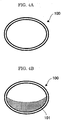
- FIG. 4A A schematic drawing of a concave portion 100 formed in the organic layer is shown in FIG. 4A .
- vacuum vapor deposition using aluminum as a fine particle material was performed at an angle of 30° to the direction perpendicular to the substrate, with the concavo-convex pattern side of the substrate facing a direction of the vacuum vapor deposition, such that a layer of the aluminum having a thickness of 30 nm was deposited on part of the concavo-convex pattern.
- aluminum fine particles 101 were formed on part of the concave portion 100.
- the substrate with the concavo-convex pattern formed on its surface was immersed in 2,2,3,3-tetrafluoro-1-propanol to dissolve the concavo-convex pattern, and aluminum fine particles were thus obtained in the solution.
- the obtained aluminum fine particles were observed using a scanning electron microscope (SEM), it was found that they were elliptical disc-shaped fine particles each having a long-side length of approximately 200 nm, a short-side length of approximately 100 nm and a thickness of approximately 30 nm.
- the dimensional variation of the long-side length was 10% as a standard deviation.
- An organic layer was formed in the same manner as in Example 1, except that the oxonol organic substance represented by the following structural formula was used instead of the oxonol organic substance represented by the above structural formula.
- the organic layer on the substrate was subjected to laser irradiation, using NEO 1000 (manufactured by Pulstec Industrial Co., Ltd.), at a pitch of 0.5 ⁇ m with respect to the radius direction and a pitch of 1.0 ⁇ m with respect to the circumferential direction and at 5 m/s and 8 mW.
- NEO 1000 manufactured by Pulstec Industrial Co., Ltd.
- the substrate with a concavo-convex pattern formed on its surface was obtained.
- a schematic drawing of a concave portion 100 formed in the organic layer is shown in FIG. 5A .
- the substrate with the concavo-convex pattern formed on its surface was immersed in 2,2,3,3-tetrafluoro-1-propanol to dissolve the concavo-convex pattern, and silver fine particles were thus obtained in the solution.
- Layer formation was carried out in the same manner as in Example 1, except that a layer of aluminum was deposited so as to have a thickness of 15 nm and then a layer of gold was deposited thereon so as to have a thickness of 15 nm at the time of vacuum vapor deposition.
- An organic layer was formed in the same manner as in Example 1, except that the phthalocyanine organic substance [(ZnPc( ⁇ -SO 2 Bu-sec) 4 ] was used instead of the oxonol organic substance represented by the above structural formula; vacuum vapor deposition using aluminum as a fine particle material was performed; a substrate with a concavo-convex pattern formed on its surface was immersed in acetone to dissolve the concavo-convex pattern; and aluminum fine particles were thus obtained in the solution.
- the phthalocyanine organic substance [(ZnPc( ⁇ -SO 2 Bu-sec) 4 ] was used instead of the oxonol organic substance represented by the above structural formula
- vacuum vapor deposition using aluminum as a fine particle material was performed; a substrate with a concavo-convex pattern formed on its surface was immersed in acetone to dissolve the concavo-convex pattern; and aluminum fine particles were thus obtained in the solution.
- An organic layer was formed in the same manner as in Example 1, except that the azo organic substance represented by the following structural formula was used instead of the oxonol organic substance represented by the above structural formula.
- the organic layer on the substrate was subjected to laser irradiation, using NEO 1000 (manufactured by Pulstec Industrial Co., Ltd.), at a pitch of 1 ⁇ m with respect to the radius direction and a pitch of 2 ⁇ m with respect to the circumferential direction and at 5 m/s and 8 mW.
- NEO 1000 manufactured by Pulstec Industrial Co., Ltd.
- vacuum vapor deposition using aluminum as a fine particle material was performed at an angle of 30° to the direction perpendicular to the substrate, with the concavo-convex pattern side of the substrate facing a direction of the vacuum vapor deposition, such that a layer of the aluminum having a thickness of 100 nm was deposited on part of the concavo-convex pattern.
- the substrate with the concavo-convex pattern formed on its surface was immersed in 2,2,3,3-tetrafluoro-1-propanol to dissolve the concavo-convex pattern, and aluminum fine particles were thus obtained in the solution.
- a substrate with a concavo-convex pattern formed on its surface was obtained in the same manner as in Example 1, except that a silicon substrate was used instead of the glass substrate.
- the silicon substrate was dry-etched using as a mask the organic layer at which the concavo-convex pattern was formed, and concave portions having a depth of 100 nm were formed in the silicon substrate.
- RIE reactive ion etching
- SD640 manufactured by Dainippon Ink And Chemicals, Incorporated
- a glass substrate was UV-cured so as to form an imprint layer having a thickness of 10 ⁇ m.
- the produced imprint mold was pressed against the imprint layer on the glass substrate so as to transfer the concavo-convex pattern of the imprint mold to the imprint layer, and the imprint mold was separated from the imprint layer so as to form a concavo-convex pattern over the glass substrate (nanoimprinting method).
- Example 2 The same oxonol organic substance as the one in Example 1 was applied by spin coating onto the concavo-convex pattern formed over the glass substrate, such that the oxonol organic substance became a layer having a thickness of 150 nm.
- vacuum vapor deposition using aluminum as a fine particle material was performed at an angle of 30° to the direction perpendicular to the glass substrate, with the concavo-convex pattern side of the substrate facing a direction of the vacuum vapor deposition, such that a layer of the aluminum having a thickness of 100 nm was deposited on part of the concavo-convex pattern.
- the glass substrate with the concavo-convex pattern formed on its surface was immersed in 2,2,3,3-tetrafluoro-1-propanol to dissolve the concavo-convex pattern, and aluminum fine particles were thus obtained in the solution.
- Aluminum fine particles were formed in the same manner as in Example 1, except that the vacuum vapor deposition was performed at an angle of 90°. Consequently, some fine particles joined together.
- Fine particles were produced by thermal processing as in an Example of JP-A No. 06-28933 . Consequently, since these particles were rounded by a thermal flow, particles of material from a plurality of concave and convex portions came together, and thus the particles became two or more times larger in size.
- fine particles obtained by the method of the present invention for producing fine particles it is possible to produce particles whose dimensions can be freely adjusted, particles with high homogeneity, fine particles composed of different components, and fine particles with a laminated structure. These can be widely used in a variety of fields, notably as polarizer materials, birefringent materials and the like.
Landscapes
- Engineering & Computer Science (AREA)
- Nanotechnology (AREA)
- Chemical & Material Sciences (AREA)
- Physics & Mathematics (AREA)
- Crystallography & Structural Chemistry (AREA)
- General Physics & Mathematics (AREA)
- Mathematical Physics (AREA)
- Theoretical Computer Science (AREA)
- Condensed Matter Physics & Semiconductors (AREA)
- Manufacturing & Machinery (AREA)
- Shaping Of Tube Ends By Bending Or Straightening (AREA)
- Physical Or Chemical Processes And Apparatus (AREA)
- Manufacture Of Metal Powder And Suspensions Thereof (AREA)
- Polarising Elements (AREA)
Claims (14)
- Verfahren zur Herstellung von Feinpartikeln, umfassend:Formung einer konkav-konvexen Struktur (13, 15) auf einer Oberfläche (1a) eines Grundmaterials (1), die durch Anordnung einer Vielzahl von konvexen Elementen (13) auf der Oberfläche (1a) hergestellt wird;Formung von Feinpartikeln (3) aus einem Feinpartikelmaterial auf mindestens einem Teil der konkav-konvexen Struktur; undLoslösung der geformten Feinpartikel von der konkav-konvexen Struktur,wobei die Feinpartikel durch Vakuum-Aufdampfen geformt werden und das Vakuum-Aufdampfen in einem Winkel von 1º bis 80º in Bezug auf die Normale zu dem Grundmaterial durchgeführt wird, wobei die Seite des Grundmaterials mit der konkav-konvexen Struktur zu dem Vakuum-Aufdampfen gerichtet ist.
- Verfahren nach Anspruch 1, wobei bei der Formung der konkav-konvexen Struktur eine organische Schicht, deren Form sich bei Anwendung von Wärme verändern kann, auf der Oberfläche des Grundmaterials (1) vorgesehen ist und die organische Schicht mit verdichtetem Licht bestrahlt wird, um die konkav-konvexe Struktur (13, 15) zu formen.
- Verfahren nach Anspruch 1, wobei bei der Formung der konkav-konvexen Struktur die konkav-konvexe Struktur mithilfe eines Prägeverfahrens geformt wird, bei dem eine Prägeschicht (24) auf der Oberfläche des Grundmateriales (1) vorgesehen ist und eine Prägeform gegen die Prägeschicht (24) gedrückt wird.
- Verfahren nach Anspruch 3, wobei die Prägeform durch Ätzen unter Verwendung einer organischen Schicht als Schablone geformt wird, die durch Bestrahlung der organischen Schicht mit verdichtetem Licht mit einer konkav-konvexen Struktur versehen wird, deren Form sich bei Anwendung von Wärme verändern kann.
- Verfahren nach Anspruch 1, wobei bei dem Vakuum-Aufdampfen mindestens zwei Feinpartikelmaterialien verwendet werden, um Feinpartikel mit einem laminierten Aufbau zu formen.
- Verfahren nach Anspruch 1, wobei bei dem Vakuum-Aufdampfen mindestens zwei Feinpartikelmaterialien mit unterschiedlichen Mischverhältnissen verwendet werden, um Feinpartikel (3) zu formen, die aus unterschiedlichen Komponenten in Bezug auf eine Dickenrichtung bestehen.
- Verfahren nach einem der Ansprüche 1 bis 6, wobei die Feinpartikel (3) entweder durch Entfernen der konkav-konvexen Struktur, an der die Feinpartikel geformt werden, oder durch Trennung der Feinpartikel von der konkav-konvexen Struktur losgelöst werden.
- Verfahren nach Anspruch 7, wobei entweder das Entfernen der konkav-konvexen Struktur, an der die Feinpartikel geformt werden, oder die Trennung der Feinpartikel von der konkav-konvexen Struktur mittels Auflösung der konkav-konvexen Struktur in einem Lösungsmittel erfolgt.
- Verfahren nach einem der vorstehenden Ansprüche, wobei der untere Grenzwert des Winkels, bei dem das Vakuum-Aufdampfen durchgeführt wird, in Bezug auf die Normale zu dem Grundmaterial 5º oder größer ist.
- Verfahren nach einem der vorstehenden Ansprüche, wobei der untere Grenzwert des Winkels, bei dem das Vakuum-Aufdampfen durchgeführt wird, in Bezug auf die Normale zu dem Grundmaterial 10º oder größer ist.
- Verfahren nach einem der vorstehenden Ansprüche, wobei der obere Grenzwert des Winkels, bei dem das Vakuum-Aufdampfen durchgeführt wird, in Bezug auf die Normale zu dem Grundmaterial 70º oder kleiner ist.
- Verfahren nach einem der vorstehenden Ansprüche, wobei der obere Grenzwert des Winkels, bei dem das Vakuum-Aufdampfen durchgeführt wird, in Bezug auf die Normale zu dem Grundmaterial 60º oder kleiner ist.
- Verfahren nach einem der vorstehenden Ansprüche, wobei der obere Grenzwert des Winkels, bei dem das Vakuum-Aufdampfen durchgeführt wird, in Bezug auf die Normale zu dem Grundmaterial 50º oder kleiner ist.
- Verfahren nach einem der vorstehenden Ansprüche, wobei der Winkel, bei dem das Vakuum-Aufdampfen durchgeführt wird, 30º in Bezug auf die Normale zu dem Grundmaterial beträgt.
Applications Claiming Priority (1)
| Application Number | Priority Date | Filing Date | Title |
|---|---|---|---|
| JP2009023613A JP5261218B2 (ja) | 2009-02-04 | 2009-02-04 | 微粒子及びその製造方法 |
Publications (3)
| Publication Number | Publication Date |
|---|---|
| EP2216680A2 EP2216680A2 (de) | 2010-08-11 |
| EP2216680A3 EP2216680A3 (de) | 2013-05-29 |
| EP2216680B1 true EP2216680B1 (de) | 2018-04-04 |
Family
ID=42111618
Family Applications (1)
| Application Number | Title | Priority Date | Filing Date |
|---|---|---|---|
| EP10000365.6A Not-in-force EP2216680B1 (de) | 2009-02-04 | 2010-01-15 | Feinteilchen und Herstellungsverfahren dafür |
Country Status (3)
| Country | Link |
|---|---|
| US (1) | US8517082B2 (de) |
| EP (1) | EP2216680B1 (de) |
| JP (1) | JP5261218B2 (de) |
Families Citing this family (10)
| Publication number | Priority date | Publication date | Assignee | Title |
|---|---|---|---|---|
| CN102648438A (zh) | 2009-08-26 | 2012-08-22 | 分子制模股份有限公司 | 功能性纳米微粒 |
| JP5222916B2 (ja) * | 2010-09-17 | 2013-06-26 | シャープ株式会社 | 半導体基材の製造方法、半導体装置、および電気機器 |
| CN103282303A (zh) * | 2010-11-05 | 2013-09-04 | 分子制模股份有限公司 | 使用双释放层的功能纳米颗粒的纳米压印光刻形成 |
| KR101240751B1 (ko) * | 2010-11-25 | 2013-03-07 | 삼성전기주식회사 | 미세 금속 분말의 제조 방법 및 이를 이용하여 제조된 미세 금속 분말 |
| JP2012140692A (ja) * | 2011-01-06 | 2012-07-26 | Oike Ind Co Ltd | 金属超微粉体 |
| KR20120102319A (ko) * | 2011-03-08 | 2012-09-18 | 삼성전기주식회사 | 금속 증착 필름, 및 이를 이용한 금속 분말 |
| KR101771138B1 (ko) * | 2011-05-13 | 2017-08-25 | 삼성전자주식회사 | 와이어 그리드 편광자, 상기 와이어 그리드 편광자의 제조 방법 및 상기 와이어 그리드 편광자를 포함하는 디스플레이 패널 |
| JP5860301B2 (ja) * | 2012-02-16 | 2016-02-16 | 住友化学株式会社 | ナノマテリアル組成物及びこれを用いたナノマテリアル含有層の形成方法 |
| CN106311077A (zh) * | 2015-06-24 | 2017-01-11 | 山东双鹤机械制造股份有限公司 | 一种立式环模颗粒机的快速装夹模具 |
| CN110975757B (zh) * | 2019-12-03 | 2021-10-08 | 江苏三仪动物营养科技有限公司 | 一种浓缩饲料颗粒机 |
Family Cites Families (49)
| Publication number | Priority date | Publication date | Assignee | Title |
|---|---|---|---|---|
| DE350399C (de) | 1919-09-19 | 1922-03-20 | Qu Bernd Ziemert | Projektionsschirm |
| JPS56111804A (en) * | 1980-02-09 | 1981-09-03 | Dainippon Printing Co Ltd | Manufacture of body differing in optical property according to direction |
| US4383967A (en) * | 1980-12-04 | 1983-05-17 | Roto-Finish Company, Inc. | Automatic finishing chip process |
| JPS58175693A (ja) | 1982-04-08 | 1983-10-14 | Ricoh Co Ltd | 高密度光情報記録媒体 |
| JPS5981194A (ja) | 1982-11-01 | 1984-05-10 | Tdk Corp | 光記録媒体 |
| JPS5955795A (ja) | 1982-09-27 | 1984-03-30 | Tdk Corp | 光記録媒体 |
| JPS6018387A (ja) | 1983-07-11 | 1985-01-30 | Tdk Corp | 光記録媒体 |
| JPS6019587A (ja) | 1983-07-13 | 1985-01-31 | Tdk Corp | 光記録媒体 |
| JPS6019586A (ja) | 1983-07-13 | 1985-01-31 | Tdk Corp | 光記録媒体 |
| JPS6035054A (ja) | 1983-08-05 | 1985-02-22 | Tdk Corp | 光記録媒体 |
| JPS6036190A (ja) | 1983-08-09 | 1985-02-25 | Tdk Corp | 光記録媒体 |
| JPS6036191A (ja) | 1983-08-09 | 1985-02-25 | Tdk Corp | 光記録媒体 |
| JPS6044554A (ja) | 1983-08-20 | 1985-03-09 | Tdk Corp | 光記録媒体 |
| JPS6044555A (ja) | 1983-08-20 | 1985-03-09 | Tdk Corp | 光記録媒体 |
| JPS6044389A (ja) | 1983-08-23 | 1985-03-09 | Tdk Corp | 光記録媒体 |
| JPS6044390A (ja) | 1983-08-23 | 1985-03-09 | Tdk Corp | 光記録媒体 |
| JPS6047069A (ja) | 1983-08-24 | 1985-03-14 | Tdk Corp | 光記録媒体 |
| JPS6054892A (ja) | 1983-09-05 | 1985-03-29 | Tdk Corp | 光記録媒体 |
| JPH0626028B2 (ja) | 1984-02-06 | 1994-04-06 | 株式会社リコー | 光情報記録媒体 |
| JPH0671830B2 (ja) * | 1985-08-06 | 1994-09-14 | 日本放送協会 | 光記録媒体および光記録方法 |
| JPS63209995A (ja) | 1987-02-27 | 1988-08-31 | Fuji Photo Film Co Ltd | 光学的情報記録媒体 |
| JPS63316407A (ja) * | 1987-06-19 | 1988-12-23 | Honda Motor Co Ltd | 永久磁石用原料粉の製造方法 |
| JP3009909B2 (ja) | 1990-05-21 | 2000-02-14 | ティーディーケイ株式会社 | 光記録媒体 |
| JPH0474690A (ja) | 1990-07-17 | 1992-03-10 | Ricoh Co Ltd | 光情報記録媒体 |
| JP2849283B2 (ja) | 1992-07-08 | 1999-01-20 | アルプス電気株式会社 | 導電性粒子の製造方法 |
| JP3451752B2 (ja) | 1994-10-31 | 2003-09-29 | ソニー株式会社 | 光記録媒体 |
| JP3096239B2 (ja) | 1996-04-01 | 2000-10-10 | 太陽誘電株式会社 | 光ディスクのランニングopc方法及び光ディスク記録再生装置 |
| JPH10235748A (ja) * | 1997-02-27 | 1998-09-08 | Seiko Epson Corp | 導光体の製造方法 |
| JPH1153758A (ja) | 1997-07-30 | 1999-02-26 | Mitsubishi Chem Corp | 記録再生方法 |
| JPH1150112A (ja) * | 1997-07-31 | 1999-02-23 | Hokuriku Electric Ind Co Ltd | 金属超微粒子粉体とその製造方法並びにその使用方法 |
| JPH11199795A (ja) * | 1998-01-16 | 1999-07-27 | Toyota Motor Corp | エンボス模様付き金属微細片の製造方法 |
| GB2334347B (en) * | 1998-02-13 | 2001-02-28 | Univ Hertfordshire | An improved method of fabricating coded particles |
| JPH11334206A (ja) | 1998-05-27 | 1999-12-07 | Mitsubishi Chemical Corp | 光学記録媒体 |
| JP3438587B2 (ja) | 1998-05-27 | 2003-08-18 | 三菱化学株式会社 | 光学記録媒体 |
| JP3646563B2 (ja) | 1998-05-27 | 2005-05-11 | 三菱化学株式会社 | 光学記録媒体 |
| JPH11334204A (ja) | 1998-05-27 | 1999-12-07 | Mitsubishi Chemical Corp | 光学記録媒体 |
| JP3633279B2 (ja) | 1998-05-27 | 2005-03-30 | 三菱化学株式会社 | 光学記録媒体 |
| JP2000108513A (ja) | 1998-10-05 | 2000-04-18 | Mitsui Chemicals Inc | 光記録媒体 |
| JP2000158818A (ja) | 1998-12-01 | 2000-06-13 | Mitsui Chemicals Inc | 光記録媒体 |
| US20040178076A1 (en) * | 1999-10-01 | 2004-09-16 | Stonas Walter J. | Method of manufacture of colloidal rod particles as nanobarcodes |
| JP2001330728A (ja) | 2000-05-22 | 2001-11-30 | Jasco Corp | ワイヤーグリット型偏光子及びその製造方法 |
| JP2003147415A (ja) * | 2001-11-15 | 2003-05-21 | Nau Chemical:Kk | 金属ボールの製造方法 |
| WO2007094829A2 (en) * | 2005-11-07 | 2007-08-23 | The University Of North Carolina At Chapel Hill | Isolated and fixed micro and nano structures and methods thereof |
| GB0605360D0 (en) * | 2006-03-16 | 2006-04-26 | Dupont Teijin Films Us Ltd | Method of manufacture |
| JP2008142895A (ja) * | 2006-12-05 | 2008-06-26 | Fujifilm Corp | モールド構造体 |
| JP5078488B2 (ja) * | 2007-03-05 | 2012-11-21 | 富士フイルム株式会社 | 発光素子およびその製造方法ならびに光学素子およびその製造方法 |
| EP2173509A4 (de) * | 2007-06-25 | 2013-11-06 | Affymetrix Inc | Strukturierte mikrocodes |
| CN102648438A (zh) * | 2009-08-26 | 2012-08-22 | 分子制模股份有限公司 | 功能性纳米微粒 |
| KR20120128686A (ko) | 2010-02-18 | 2012-11-27 | 심포젠 에이/에스 | 녹농균의 혈청형 a 지질다당류에 대한 항체 |
-
2009
- 2009-02-04 JP JP2009023613A patent/JP5261218B2/ja not_active Expired - Fee Related
-
2010
- 2010-01-15 EP EP10000365.6A patent/EP2216680B1/de not_active Not-in-force
- 2010-02-04 US US12/699,915 patent/US8517082B2/en not_active Expired - Fee Related
Non-Patent Citations (1)
| Title |
|---|
| None * |
Also Published As
| Publication number | Publication date |
|---|---|
| US20100196713A1 (en) | 2010-08-05 |
| EP2216680A2 (de) | 2010-08-11 |
| EP2216680A3 (de) | 2013-05-29 |
| JP5261218B2 (ja) | 2013-08-14 |
| US8517082B2 (en) | 2013-08-27 |
| JP2010180442A (ja) | 2010-08-19 |
Similar Documents
| Publication | Publication Date | Title |
|---|---|---|
| EP2216680B1 (de) | Feinteilchen und Herstellungsverfahren dafür | |
| US8574469B2 (en) | Processing method and manufacturing method for optical component | |
| US20100294536A1 (en) | Transparent conductor and production method thereof | |
| EP2219053A1 (de) | Wärmestrahlungs-Reflexionsfolie, Wärmestrahlungs-Reflexionsstruktur und Herstellungsverfahren dafür | |
| US8323762B2 (en) | Method for manufacturing medium on which information is recorded in pit pattern | |
| JP5518541B2 (ja) | ナノ粒子の製造方法及び量子ドットの製造方法 | |
| KR101339751B1 (ko) | 발광 소자와 그 제조 방법 및 광학 소자와 그 제조 방법 | |
| EP2110814B1 (de) | Herstellungsverfahren für einen Stanzer und Herstellungsverfahren für ein optisches Informationsaufzeichnungsmedium, das diesen Stanzer verwendet | |
| JP2009279831A (ja) | 曲面状部材、曲面状部材の製造方法および金型の製造方法 | |
| US20110129634A1 (en) | Patterned member and method for manufacturing the patterned member | |
| CN101828228B (zh) | 凹部形成方法、凹-凸制品的制造方法、发光元件的制造方法和光学元件的制造方法 | |
| JP4950101B2 (ja) | フォトレジスト層を有するワークの加工方法 | |
| JP2012135767A (ja) | 被加工物の加工方法 | |
| US20100236584A1 (en) | Method for cleaning heat mode type recording material layer, method for manufacturing pit-projection product, method for manufacturing light emitting element, and method for manufacturing optical element | |
| JP2009282278A (ja) | フォトレジスト層の加工方法および曲面状部材の製造方法 | |
| JP2009282277A (ja) | フォトレジスト層の加工方法およびパターン形成基板の製造方法 | |
| JP2010184288A (ja) | レーザ加工方法 |
Legal Events
| Date | Code | Title | Description |
|---|---|---|---|
| PUAI | Public reference made under article 153(3) epc to a published international application that has entered the european phase |
Free format text: ORIGINAL CODE: 0009012 |
|
| AK | Designated contracting states |
Kind code of ref document: A2 Designated state(s): AT BE BG CH CY CZ DE DK EE ES FI FR GB GR HR HU IE IS IT LI LT LU LV MC MK MT NL NO PL PT RO SE SI SK SM TR |
|
| AX | Request for extension of the european patent |
Extension state: AL BA RS |
|
| PUAL | Search report despatched |
Free format text: ORIGINAL CODE: 0009013 |
|
| AK | Designated contracting states |
Kind code of ref document: A3 Designated state(s): AT BE BG CH CY CZ DE DK EE ES FI FR GB GR HR HU IE IS IT LI LT LU LV MC MK MT NL NO PL PT RO SE SI SK SM TR |
|
| AX | Request for extension of the european patent |
Extension state: AL BA RS |
|
| RIC1 | Information provided on ipc code assigned before grant |
Ipc: G03F 7/00 20060101AFI20130423BHEP Ipc: B01J 2/22 20060101ALI20130423BHEP |
|
| 17P | Request for examination filed |
Effective date: 20130904 |
|
| RBV | Designated contracting states (corrected) |
Designated state(s): AT BE BG CH CY CZ DE DK EE ES FI FR GB GR HR HU IE IS IT LI LT LU LV MC MK MT NL NO PL PT RO SE SI SK SM TR |
|
| GRAP | Despatch of communication of intention to grant a patent |
Free format text: ORIGINAL CODE: EPIDOSNIGR1 |
|
| STAA | Information on the status of an ep patent application or granted ep patent |
Free format text: STATUS: GRANT OF PATENT IS INTENDED |
|
| INTG | Intention to grant announced |
Effective date: 20180118 |
|
| GRAS | Grant fee paid |
Free format text: ORIGINAL CODE: EPIDOSNIGR3 |
|
| GRAA | (expected) grant |
Free format text: ORIGINAL CODE: 0009210 |
|
| STAA | Information on the status of an ep patent application or granted ep patent |
Free format text: STATUS: THE PATENT HAS BEEN GRANTED |
|
| AK | Designated contracting states |
Kind code of ref document: B1 Designated state(s): AT BE BG CH CY CZ DE DK EE ES FI FR GB GR HR HU IE IS IT LI LT LU LV MC MK MT NL NO PL PT RO SE SI SK SM TR |
|
| REG | Reference to a national code |
Ref country code: GB Ref legal event code: FG4D |
|
| REG | Reference to a national code |
Ref country code: CH Ref legal event code: EP |
|
| REG | Reference to a national code |
Ref country code: AT Ref legal event code: REF Ref document number: 986219 Country of ref document: AT Kind code of ref document: T Effective date: 20180415 |
|
| REG | Reference to a national code |
Ref country code: IE Ref legal event code: FG4D |
|
| REG | Reference to a national code |
Ref country code: DE Ref legal event code: R096 Ref document number: 602010049587 Country of ref document: DE |
|
| REG | Reference to a national code |
Ref country code: NL Ref legal event code: MP Effective date: 20180404 |
|
| REG | Reference to a national code |
Ref country code: LT Ref legal event code: MG4D |
|
| PG25 | Lapsed in a contracting state [announced via postgrant information from national office to epo] |
Ref country code: NL Free format text: LAPSE BECAUSE OF FAILURE TO SUBMIT A TRANSLATION OF THE DESCRIPTION OR TO PAY THE FEE WITHIN THE PRESCRIBED TIME-LIMIT Effective date: 20180404 |
|
| PG25 | Lapsed in a contracting state [announced via postgrant information from national office to epo] |
Ref country code: SE Free format text: LAPSE BECAUSE OF FAILURE TO SUBMIT A TRANSLATION OF THE DESCRIPTION OR TO PAY THE FEE WITHIN THE PRESCRIBED TIME-LIMIT Effective date: 20180404 Ref country code: ES Free format text: LAPSE BECAUSE OF FAILURE TO SUBMIT A TRANSLATION OF THE DESCRIPTION OR TO PAY THE FEE WITHIN THE PRESCRIBED TIME-LIMIT Effective date: 20180404 Ref country code: LT Free format text: LAPSE BECAUSE OF FAILURE TO SUBMIT A TRANSLATION OF THE DESCRIPTION OR TO PAY THE FEE WITHIN THE PRESCRIBED TIME-LIMIT Effective date: 20180404 Ref country code: PL Free format text: LAPSE BECAUSE OF FAILURE TO SUBMIT A TRANSLATION OF THE DESCRIPTION OR TO PAY THE FEE WITHIN THE PRESCRIBED TIME-LIMIT Effective date: 20180404 Ref country code: NO Free format text: LAPSE BECAUSE OF FAILURE TO SUBMIT A TRANSLATION OF THE DESCRIPTION OR TO PAY THE FEE WITHIN THE PRESCRIBED TIME-LIMIT Effective date: 20180704 Ref country code: FI Free format text: LAPSE BECAUSE OF FAILURE TO SUBMIT A TRANSLATION OF THE DESCRIPTION OR TO PAY THE FEE WITHIN THE PRESCRIBED TIME-LIMIT Effective date: 20180404 Ref country code: BG Free format text: LAPSE BECAUSE OF FAILURE TO SUBMIT A TRANSLATION OF THE DESCRIPTION OR TO PAY THE FEE WITHIN THE PRESCRIBED TIME-LIMIT Effective date: 20180704 |
|
| PG25 | Lapsed in a contracting state [announced via postgrant information from national office to epo] |
Ref country code: HR Free format text: LAPSE BECAUSE OF FAILURE TO SUBMIT A TRANSLATION OF THE DESCRIPTION OR TO PAY THE FEE WITHIN THE PRESCRIBED TIME-LIMIT Effective date: 20180404 Ref country code: LV Free format text: LAPSE BECAUSE OF FAILURE TO SUBMIT A TRANSLATION OF THE DESCRIPTION OR TO PAY THE FEE WITHIN THE PRESCRIBED TIME-LIMIT Effective date: 20180404 Ref country code: GR Free format text: LAPSE BECAUSE OF FAILURE TO SUBMIT A TRANSLATION OF THE DESCRIPTION OR TO PAY THE FEE WITHIN THE PRESCRIBED TIME-LIMIT Effective date: 20180705 |
|
| REG | Reference to a national code |
Ref country code: AT Ref legal event code: MK05 Ref document number: 986219 Country of ref document: AT Kind code of ref document: T Effective date: 20180404 |
|
| PG25 | Lapsed in a contracting state [announced via postgrant information from national office to epo] |
Ref country code: PT Free format text: LAPSE BECAUSE OF FAILURE TO SUBMIT A TRANSLATION OF THE DESCRIPTION OR TO PAY THE FEE WITHIN THE PRESCRIBED TIME-LIMIT Effective date: 20180806 |
|
| REG | Reference to a national code |
Ref country code: DE Ref legal event code: R097 Ref document number: 602010049587 Country of ref document: DE |
|
| PG25 | Lapsed in a contracting state [announced via postgrant information from national office to epo] |
Ref country code: AT Free format text: LAPSE BECAUSE OF FAILURE TO SUBMIT A TRANSLATION OF THE DESCRIPTION OR TO PAY THE FEE WITHIN THE PRESCRIBED TIME-LIMIT Effective date: 20180404 Ref country code: DK Free format text: LAPSE BECAUSE OF FAILURE TO SUBMIT A TRANSLATION OF THE DESCRIPTION OR TO PAY THE FEE WITHIN THE PRESCRIBED TIME-LIMIT Effective date: 20180404 Ref country code: SK Free format text: LAPSE BECAUSE OF FAILURE TO SUBMIT A TRANSLATION OF THE DESCRIPTION OR TO PAY THE FEE WITHIN THE PRESCRIBED TIME-LIMIT Effective date: 20180404 Ref country code: EE Free format text: LAPSE BECAUSE OF FAILURE TO SUBMIT A TRANSLATION OF THE DESCRIPTION OR TO PAY THE FEE WITHIN THE PRESCRIBED TIME-LIMIT Effective date: 20180404 Ref country code: CZ Free format text: LAPSE BECAUSE OF FAILURE TO SUBMIT A TRANSLATION OF THE DESCRIPTION OR TO PAY THE FEE WITHIN THE PRESCRIBED TIME-LIMIT Effective date: 20180404 Ref country code: RO Free format text: LAPSE BECAUSE OF FAILURE TO SUBMIT A TRANSLATION OF THE DESCRIPTION OR TO PAY THE FEE WITHIN THE PRESCRIBED TIME-LIMIT Effective date: 20180404 |
|
| PLBE | No opposition filed within time limit |
Free format text: ORIGINAL CODE: 0009261 |
|
| STAA | Information on the status of an ep patent application or granted ep patent |
Free format text: STATUS: NO OPPOSITION FILED WITHIN TIME LIMIT |
|
| PG25 | Lapsed in a contracting state [announced via postgrant information from national office to epo] |
Ref country code: SM Free format text: LAPSE BECAUSE OF FAILURE TO SUBMIT A TRANSLATION OF THE DESCRIPTION OR TO PAY THE FEE WITHIN THE PRESCRIBED TIME-LIMIT Effective date: 20180404 Ref country code: IT Free format text: LAPSE BECAUSE OF FAILURE TO SUBMIT A TRANSLATION OF THE DESCRIPTION OR TO PAY THE FEE WITHIN THE PRESCRIBED TIME-LIMIT Effective date: 20180404 |
|
| 26N | No opposition filed |
Effective date: 20190107 |
|
| PGFP | Annual fee paid to national office [announced via postgrant information from national office to epo] |
Ref country code: GB Payment date: 20190109 Year of fee payment: 10 Ref country code: DE Payment date: 20190102 Year of fee payment: 10 |
|
| PG25 | Lapsed in a contracting state [announced via postgrant information from national office to epo] |
Ref country code: SI Free format text: LAPSE BECAUSE OF FAILURE TO SUBMIT A TRANSLATION OF THE DESCRIPTION OR TO PAY THE FEE WITHIN THE PRESCRIBED TIME-LIMIT Effective date: 20180404 |
|
| PG25 | Lapsed in a contracting state [announced via postgrant information from national office to epo] |
Ref country code: MC Free format text: LAPSE BECAUSE OF FAILURE TO SUBMIT A TRANSLATION OF THE DESCRIPTION OR TO PAY THE FEE WITHIN THE PRESCRIBED TIME-LIMIT Effective date: 20180404 |
|
| REG | Reference to a national code |
Ref country code: CH Ref legal event code: PL |
|
| PG25 | Lapsed in a contracting state [announced via postgrant information from national office to epo] |
Ref country code: LU Free format text: LAPSE BECAUSE OF NON-PAYMENT OF DUE FEES Effective date: 20190115 |
|
| REG | Reference to a national code |
Ref country code: BE Ref legal event code: MM Effective date: 20190131 |
|
| REG | Reference to a national code |
Ref country code: IE Ref legal event code: MM4A |
|
| PG25 | Lapsed in a contracting state [announced via postgrant information from national office to epo] |
Ref country code: BE Free format text: LAPSE BECAUSE OF NON-PAYMENT OF DUE FEES Effective date: 20190131 |
|
| PG25 | Lapsed in a contracting state [announced via postgrant information from national office to epo] |
Ref country code: LI Free format text: LAPSE BECAUSE OF NON-PAYMENT OF DUE FEES Effective date: 20190131 Ref country code: CH Free format text: LAPSE BECAUSE OF NON-PAYMENT OF DUE FEES Effective date: 20190131 |
|
| PG25 | Lapsed in a contracting state [announced via postgrant information from national office to epo] |
Ref country code: IE Free format text: LAPSE BECAUSE OF NON-PAYMENT OF DUE FEES Effective date: 20190115 |
|
| PGFP | Annual fee paid to national office [announced via postgrant information from national office to epo] |
Ref country code: FR Payment date: 20191216 Year of fee payment: 11 |
|
| PG25 | Lapsed in a contracting state [announced via postgrant information from national office to epo] |
Ref country code: TR Free format text: LAPSE BECAUSE OF FAILURE TO SUBMIT A TRANSLATION OF THE DESCRIPTION OR TO PAY THE FEE WITHIN THE PRESCRIBED TIME-LIMIT Effective date: 20180404 |
|
| PG25 | Lapsed in a contracting state [announced via postgrant information from national office to epo] |
Ref country code: MT Free format text: LAPSE BECAUSE OF NON-PAYMENT OF DUE FEES Effective date: 20190115 |
|
| REG | Reference to a national code |
Ref country code: DE Ref legal event code: R119 Ref document number: 602010049587 Country of ref document: DE |
|
| GBPC | Gb: european patent ceased through non-payment of renewal fee |
Effective date: 20200115 |
|
| PG25 | Lapsed in a contracting state [announced via postgrant information from national office to epo] |
Ref country code: DE Free format text: LAPSE BECAUSE OF NON-PAYMENT OF DUE FEES Effective date: 20200801 Ref country code: GB Free format text: LAPSE BECAUSE OF NON-PAYMENT OF DUE FEES Effective date: 20200115 |
|
| PG25 | Lapsed in a contracting state [announced via postgrant information from national office to epo] |
Ref country code: CY Free format text: LAPSE BECAUSE OF FAILURE TO SUBMIT A TRANSLATION OF THE DESCRIPTION OR TO PAY THE FEE WITHIN THE PRESCRIBED TIME-LIMIT Effective date: 20180404 |
|
| PG25 | Lapsed in a contracting state [announced via postgrant information from national office to epo] |
Ref country code: IS Free format text: LAPSE BECAUSE OF FAILURE TO SUBMIT A TRANSLATION OF THE DESCRIPTION OR TO PAY THE FEE WITHIN THE PRESCRIBED TIME-LIMIT Effective date: 20180804 |
|
| PG25 | Lapsed in a contracting state [announced via postgrant information from national office to epo] |
Ref country code: HU Free format text: LAPSE BECAUSE OF FAILURE TO SUBMIT A TRANSLATION OF THE DESCRIPTION OR TO PAY THE FEE WITHIN THE PRESCRIBED TIME-LIMIT; INVALID AB INITIO Effective date: 20100115 |
|
| PG25 | Lapsed in a contracting state [announced via postgrant information from national office to epo] |
Ref country code: FR Free format text: LAPSE BECAUSE OF NON-PAYMENT OF DUE FEES Effective date: 20210131 |
|
| PG25 | Lapsed in a contracting state [announced via postgrant information from national office to epo] |
Ref country code: MK Free format text: LAPSE BECAUSE OF FAILURE TO SUBMIT A TRANSLATION OF THE DESCRIPTION OR TO PAY THE FEE WITHIN THE PRESCRIBED TIME-LIMIT Effective date: 20180404 |