EP2197118B1 - A/d converting circuit, solid-state image sensing device and camera system - Google Patents
A/d converting circuit, solid-state image sensing device and camera system Download PDFInfo
- Publication number
- EP2197118B1 EP2197118B1 EP08834294.4A EP08834294A EP2197118B1 EP 2197118 B1 EP2197118 B1 EP 2197118B1 EP 08834294 A EP08834294 A EP 08834294A EP 2197118 B1 EP2197118 B1 EP 2197118B1
- Authority
- EP
- European Patent Office
- Prior art keywords
- data
- output
- counter
- input
- circuit
- Prior art date
- Legal status (The legal status is an assumption and is not a legal conclusion. Google has not performed a legal analysis and makes no representation as to the accuracy of the status listed.)
- Not-in-force
Links
Images


Classifications
-
- H—ELECTRICITY
- H04—ELECTRIC COMMUNICATION TECHNIQUE
- H04N—PICTORIAL COMMUNICATION, e.g. TELEVISION
- H04N25/00—Circuitry of solid-state image sensors [SSIS]; Control thereof
- H04N25/70—SSIS architectures; Circuits associated therewith
- H04N25/71—Charge-coupled device [CCD] sensors; Charge-transfer registers specially adapted for CCD sensors
- H04N25/75—Circuitry for providing, modifying or processing image signals from the pixel array
-
- H—ELECTRICITY
- H04—ELECTRIC COMMUNICATION TECHNIQUE
- H04N—PICTORIAL COMMUNICATION, e.g. TELEVISION
- H04N25/00—Circuitry of solid-state image sensors [SSIS]; Control thereof
- H04N25/60—Noise processing, e.g. detecting, correcting, reducing or removing noise
- H04N25/65—Noise processing, e.g. detecting, correcting, reducing or removing noise applied to reset noise, e.g. KTC noise related to CMOS structures by techniques other than CDS
-
- H—ELECTRICITY
- H03—ELECTRONIC CIRCUITRY
- H03K—PULSE TECHNIQUE
- H03K23/00—Pulse counters comprising counting chains; Frequency dividers comprising counting chains
- H03K23/58—Gating or clocking signals not applied to all stages, i.e. asynchronous counters
- H03K23/62—Gating or clocking signals not applied to all stages, i.e. asynchronous counters reversible
-
- H—ELECTRICITY
- H03—ELECTRONIC CIRCUITRY
- H03M—CODING; DECODING; CODE CONVERSION IN GENERAL
- H03M1/00—Analogue/digital conversion; Digital/analogue conversion
- H03M1/10—Calibration or testing
- H03M1/1009—Calibration
- H03M1/1014—Calibration at one point of the transfer characteristic, i.e. by adjusting a single reference value, e.g. bias or gain error
- H03M1/1023—Offset correction
-
- H—ELECTRICITY
- H03—ELECTRONIC CIRCUITRY
- H03M—CODING; DECODING; CODE CONVERSION IN GENERAL
- H03M1/00—Analogue/digital conversion; Digital/analogue conversion
- H03M1/12—Analogue/digital converters
-
- H—ELECTRICITY
- H03—ELECTRONIC CIRCUITRY
- H03M—CODING; DECODING; CODE CONVERSION IN GENERAL
- H03M1/00—Analogue/digital conversion; Digital/analogue conversion
- H03M1/12—Analogue/digital converters
- H03M1/124—Sampling or signal conditioning arrangements specially adapted for A/D converters
- H03M1/129—Means for adapting the input signal to the range the converter can handle, e.g. limiting, pre-scaling ; Out-of-range indication
- H03M1/1295—Clamping, i.e. adjusting the DC level of the input signal to a predetermined value
-
- H—ELECTRICITY
- H03—ELECTRONIC CIRCUITRY
- H03M—CODING; DECODING; CODE CONVERSION IN GENERAL
- H03M1/00—Analogue/digital conversion; Digital/analogue conversion
- H03M1/12—Analogue/digital converters
- H03M1/20—Increasing resolution using an n bit system to obtain n + m bits
-
- H—ELECTRICITY
- H03—ELECTRONIC CIRCUITRY
- H03M—CODING; DECODING; CODE CONVERSION IN GENERAL
- H03M1/00—Analogue/digital conversion; Digital/analogue conversion
- H03M1/12—Analogue/digital converters
- H03M1/50—Analogue/digital converters with intermediate conversion to time interval
- H03M1/56—Input signal compared with linear ramp
-
- H—ELECTRICITY
- H04—ELECTRIC COMMUNICATION TECHNIQUE
- H04N—PICTORIAL COMMUNICATION, e.g. TELEVISION
- H04N25/00—Circuitry of solid-state image sensors [SSIS]; Control thereof
-
- H—ELECTRICITY
- H04—ELECTRIC COMMUNICATION TECHNIQUE
- H04N—PICTORIAL COMMUNICATION, e.g. TELEVISION
- H04N25/00—Circuitry of solid-state image sensors [SSIS]; Control thereof
- H04N25/60—Noise processing, e.g. detecting, correcting, reducing or removing noise
- H04N25/616—Noise processing, e.g. detecting, correcting, reducing or removing noise involving a correlated sampling function, e.g. correlated double sampling [CDS] or triple sampling
-
- H—ELECTRICITY
- H04—ELECTRIC COMMUNICATION TECHNIQUE
- H04N—PICTORIAL COMMUNICATION, e.g. TELEVISION
- H04N25/00—Circuitry of solid-state image sensors [SSIS]; Control thereof
- H04N25/70—SSIS architectures; Circuits associated therewith
- H04N25/76—Addressed sensors, e.g. MOS or CMOS sensors
- H04N25/78—Readout circuits for addressed sensors, e.g. output amplifiers or A/D converters
-
- H—ELECTRICITY
- H03—ELECTRONIC CIRCUITRY
- H03M—CODING; DECODING; CODE CONVERSION IN GENERAL
- H03M1/00—Analogue/digital conversion; Digital/analogue conversion
- H03M1/12—Analogue/digital converters
- H03M1/1205—Multiplexed conversion systems
- H03M1/123—Simultaneous, i.e. using one converter per channel but with common control or reference circuits for multiple converters
Definitions
- the present invention relates to an A/D conversion circuit that can be applied to parallel-column output-type CMOS image sensors or the like, a solid-state image sensor using the A/D conversion circuit, and a camera system.
- CMOS image sensors For manufacturing CMOS image sensors, it is possible to use manufacturing processes that are the same as those used for typical CMOS-type integrated circuits, also driving using a single power source is possible, and furthermore, analog circuits and logic circuits employing CMOS processes can be made to coexist in the same chip. Therefore, CMOS image sensors have a plurality of significant merits, such as it being possible to decrease the number of peripheral ICs.
- CMOS image sensors In contrast, for CMOS image sensors, an FD amplifier is provided for each pixel, and it is usually the case that parallel-column output-types are used in which a certain row within a pixel array is selected and the pixels are simultaneously read in the column direction.
- noise having a reverse correlation with a sampling capacitance value is carried.
- a potential slope is used, and signal charge is completely transferred. Therefore, noise is not generated in this sampling process, but noise is carried when the voltage level of the preceding capacitor is reset to a certain reference value.
- CDS correlated double sampling
- CMOS image sensors There are various specific methods for CDS.
- One of most advanced forms regarding signal output circuits of parallel-column output-type CMOS image sensors is a type in which an analog-digital (A/D) conversion circuit (ADC (analog digital converter)) is provided for each column, and a pixel signal is extracted as a digital signal.
- A/D analog-digital
- ADC analog digital converter
- CMOS image sensor having such a parallel column-type ADC mounted therein is disclosed in, for example, W. Yang et al. ( W. Yang et. Al., "An Integrated 800x600 CMOS Image System, "ISSCC Digest of Technical Papers, pp. 304-305, Feb., 1999 ), Japanese Unexamined Patent Application Publication No. 2005-303648 , and Japanese Unexamined Patent Application Publication No. 2005-323331 .
- JP 2005/311933 A discloses an asynchronous counter that is capable of switching count mode.
- the counter includes flip-flops and three-input single-output tri-value switches respectively provided between the adjacent pairs of the flip-flops.
- the tri-value switches switch among three values, namely, non-inverting outputs and inverting outputs of the flip-flops and a power supply level.
- Each of the tri-value switches switch among the three input signals according to two-bit control signals, and input a selected signal to a clock terminal of a subsequent flip-flop.
- A/D conversion circuit constituted by a counter, a comparator, and a reference voltage generator is used, a reset level is A/D converted by down count, and next, the signal level is A/D converted by up-count while the value is held, thereby performing CDS by differential computation of digital data.
- the present invention aims to provide an A/D conversion circuit in which a counter is made to be capable of performing counting at both edges of a clock, up/down count values can be switched while the up/down count values are held, and it is difficult for the duty of the counting operation to become distorted even with the both-edge counting, a solid-state image sensor, and a camera system.
- a counter that performs a counting operation at both rising and falling edges of an input clock is used. Then, in the present invention, by using a counter for both-edge counting of a clock, with which this counting operation is realized, up/down count values are switched while the up/down count values are held.
- a counter is made to be capable of performing counting at both edges of a clock and switching up/down count values while the up/down count values are held and the duty of a counting operation is difficult to be distorted even with the both-edge counting.
- Fig. 1 is a block diagram showing an example of the configuration of a parallel column ADC-mounted solid-state image sensor (CMOS image sensor) including a data transfer circuit according to an embodiment of the present invention.
- CMOS image sensor solid-state image sensor
- Fig. 2 shows operation waveforms of the solid-state image sensor of Fig. 1 .
- the solid-state image sensor 10 includes a pixel array unit 11 serving as an image-capturing unit, a row scanning circuit 12, a column scanning circuit 13, a timing control circuit 14, an ADC group 15, a digital-analog conversion circuit (hereinafter abbreviated as a "DAC (digital-analog converter)) 16 serving as a reference voltage generation circuit, and a data output circuit 17 having a sensing amplifier circuit (S/A), and the like.
- DAC digital-analog converter
- the pixel array unit 11 is formed in such a manner that unit pixels 111 including a photodiode and an intra-pixel amplifier are arranged in a matrix.
- the timing control circuit 14 for generating an internal clock the row scanning circuit 12 for controlling row addressing and row scanning, and the column scanning circuit 13 for controlling column addressing and column scanning are arranged.
- an ADC (A/D conversion circuit) 15A formed of (n+1) comparators (CMPs) 151 provided in correspondence with each column of pixel arrangement that compares a ramp waveform RAMP in which a reference voltage generated by the DAC 16 is changed in a step-like manner with an analog signal obtained from the unit pixel 111 through column lines V0, V1... for each of the row lines H0, H1..., and up/down counters (hereinafter referred to as counters, CNT) 152 having functions of performing up counting (or down counting) upon receipt of the output of the comparator 151 and the clock CK, and holding the count value is arranged for each of the column lines V0, V1... in such a manner as to correspond to each column of the pixel arrangement, thereby forming a parallel column ADC block 153.
- CMPs comparators
- each counter 152 is connected to a data transfer line 18 via a switch 154.
- the data output circuit 17 including a sensing circuit and a subtraction circuit, which correspond to the data transfer line 18, is arranged.
- the counter 152 having a function as a holding circuit is, for example, in an up-count (or down-count) state.
- the up-count operation is stopped, and the count value is held.
- the initial values of the counters 152 are set to, for example, an arbitrary value of the gradations of AD conversion, for example, 0.
- reset components ⁇ V of the unit pixels 111 are read.
- the counters 152 enter a down-count (or up-count) state and perform data counting corresponding to the amount of incident light.
- the count value corresponding to the comparison period is held.
- the held counter value is scanned by the column scanning circuit 13 and is input as a digital signal to the output circuit 17 after passing through the data transfer line 18.
- the column scanning circuit 13 is activated as a result of, for example, a start pulse STR and a master clock MCK being supplied, drives a corresponding selection line SEL in synchronization with a driving clock CLK in accordance with the master clock MCK (MCK is used as a reference), and causes the data transfer line 18 to read the latched data of the counter 152.
- the following processing is performed in one horizontal unit period (1H).
- Timing control of the P-phase reading PR, the P-phase comparison PC, the D-phase reading DR, the D-phase comparison DC, and the D-phase post-processing DAP is performed by the timing control circuit 14.
- the ADC 15A is configured as an integrating-type A/D conversion circuit in which the comparator 151 and the asynchronous counter 152 are used.
- the counter 152 has functions of capable of switching the count mode from an up count to a down count and from a down count to an up count while a value is held.
- the counter 152 has functions of performing counting at both the rising and falling edges of the input clock CK and performing counting at a frequency two times as high as the input clock.
- the counter 152 has functions of asynchronously latching the input clock CK in response to an asynchronous signal of the output of the comparator 151 and setting the non-inverted or inverted data of the latched data to be LSB data.
- the counter 152 has a latch circuit that latches an input clock CK, which includes an LSB bit circuit, and a memory for separately storing the output thereof, and has a function of switching the non-inversion and inversion of the input clock of the next bit on the basis of the memory data.
- the memory is arranged in front (comparator side) of the input unit of the input clock and the latch circuit in a physical manner.
- the counter 152 having such features will be described more specifically.
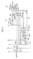
- Fig. 3 is a circuit diagram showing a specific example of the configuration of an asynchronous counter, which is one mechanism of the configuration of an up/down counter according to the present embodiment.
- Fig. 4 is a timing chart of operations of the counter of Fig. 3 .
- the counter 152 is constituted by an LSB circuit 210 that operates at the same frequency as the input clock CK and that sets the output thereof to be the LSB data of the counter 152, and a so-called ripple counter 220 configured in such a manner that circuits that divide-by-two the input signal at the immediately subsequent and following stages of the LSB circuit 210 are cascade-connected.
- the counter 152 is configured in such a form that, in addition to the LSB circuit 210 and the ripple counter 220, a logic gate part 230, such as an output logic changeover switch, for realizing a function of switching up/down while the count is held is added.
- a logic gate part 230 such as an output logic changeover switch
- the ripple counter 220 includes D-type FFs 221 to 223 and selectors 224 to 229.
- the clock terminal of the negative input of the FF 221 is connected to the supply line of the output D[0] of the selector 212 of the LSB circuit 210, and the Q output is connected to the positive and negative inputs of the selectors 224 and 225.
- the output of the selector 224 is connected to the D input of the FF 221, and the output D[1] of the selector 225 is supplied to the negative input clock terminal of the FF 222 at the next stage.
- the Q output of the FF 222 is connected to the positive and negative inputs of the selectors 226 and 227.
- the output of the selector 226 is connected to the D input of the FF 222, and the output D[2] of the selector 227 is supplied to the negative input clock terminal of the FF 223 at the next stage.
- the Q output of the FF 223 is connected to the positive and negative inputs of the selectors 228 and 229.
- the output of the selector 228 is connected to the D input of the FF 223.
- the output switching of the selectors 224 and 226 is selectively controlled in accordance with a hold signal HLD, and the output switching of the selectors 227 and 229 is selectively controlled in accordance with a control signal UD.
- the control signal UD is used to invert the output logic of each bit, with the result that data that is up-counted previously is inverted so as to be converted into complement data, thereby being changed to a down-counted result.
- the input/output of each bit is temporarily changed from negative feedback to positive feedback in accordance with the hold signal HLD, and the data of the FFs 221 to 223 is fixed in advance.
- the LSB circuit 210 includes a latch circuit 211, a selector 212, and a D-type flip-flop (FF) 213 serving as a holding unit (memory).
- FF D-type flip-flop
- the ripple counter 220 includes D-type FFs 221 to 223 and selectors 224 to 229.
- the logic gate part 230 includes two-input NAND gates 231 and 232.
- the D input of the latch circuit 211 is connected to the supply line of the clock CK, and the G input thereof is connected to the output of the logic gate part 230, and the Q output thereof is connected to the positive and negative inputs of the selector 212.
- the latch circuit 211 holds data when the G input is logic 0 (low level) and outputs the input data when the G input is logic 1 (high level).
- the output of the selector 212 is connected to the negative clock input terminal of the FF 221 of the ripple counter 220.
- the negative clock input terminal of the FF 213 is connected to the input line of the signal LL, and the Q output is connected to the switching control terminal of the selector 212.
- the output switching of the selector 212 is selectively controlled on the basis of the output of the FF 213.
- one of the input terminals of the NAND gate 231 is connected to the supply line of the output signal CompOut of the comparator 151 at the previous stage, the other input terminal is connected to the supply line of the signal EN, and the output is connected to one of the input terminals of the NAND gate 232.
- the other input terminal of the NAND gate 232 is connected to the supply line of the signal XLBD, and the output is connected to the G input of the latch circuit 211 of the LSB circuit 210.
- the latch circuit 211 upon receiving the output CompOut signal of the comparator 151 at the previous stage of the counter 152, the latch circuit 211 latches the input clock CK as is.
- a function of forcibly allowing the latch circuit 211 to be placed in a through state is effected in accordance with a signal XLBD.
- the signal EN is a control signal that causes the latch circuit 211 to be placed in a latched state by ignoring the comparator output CompOut in a case where the output of the comparator 151 enters an unstable state in a state other than the counting operation time.
- a selector 212 for switching output logic and an FF 213 for storing the output signal of the selector 212 are arranged.
- the latch circuit 211 enters a data held state from the through state of the input clock CK. Therefore, the input clock CK up to that point is counted by the counter 152.
- a data inversion operation is performed in the same manner as in the circuits other than the LSB circuit. This operation is realized by using a signal LL and a signal XLBD.
- the output data (D[0]) of the selector 212 is stored in the FF 213.
- the state of the selector is maintained.
- the latch is temporarily placed in a through state in response to the signal XLBD, thereby loading a clock initial state. In consequence, the data is inverted.
- the above control enables the operations of the LSB circuit 210 that switches output logic to be realized on the basis of the data latched in accordance with the comparator output CompOut.
- the ripple counter 220 which is a circuit for bits of other than the LSB circuit, causes the data of the FFs 221 to 223 to be placed in a held state in accordance with the hold signal HLD. In consequence, the data inversion operation of the entire counter, including the LSB, is performed without damaging the data.
- the logic switching selector 212 of the LSB circuit 210 is considered to be placed in front of the latch circuit 211. Since this counter 152 is part of the A/D conversion circuit 15A and components up to the latch circuit 211 affect the characteristics of A/D conversion (more specifically, differentiation linearity of LSB data), changes in the state up to that point cause A/D conversion characteristics to be changed, which is undesirable.
- the circuit configuration that constantly operates in the same state up to the latch circuit as in the present method has a merit of facilitating maintenance of characteristics.
- Fig. 5 is a circuit diagram showing a more specific example of the configuration of the LSB circuit according to the present embodiment.
- the latch circuit 211 is constituted by clocked inverters CINV1 and CINV2, and inverters INV1 and INV2.
- the input terminal of the clocked inverter CINV1 is connected to the supply line of the clock CK, and the output thereof is connected to the input terminal of the inverter INV2.
- the input T terminal of the inverter INV1, the negative-side control terminal of the clocked inverter CINV1, and the positive-side control terminal of the clocked inverter CINV2 are connected to the output terminals of the logic gate part 230 and the NAND gate 232.
- the output terminal of the inverter INV1 is connected to the positive-side control terminal of the clocked inverter CINV1 and the negative-side control terminal of the clocked inverter CINV2.
- the output terminal of the inverter INV2 is connected to the input terminal of the clocked inverter CINV2 and the input terminal of the selector 212.
- the selector 212 is constituted by clocked inverters CINV3, CINV4, and CINV5, and an inverter INV3.
- the input terminals of the clocked inverters CINV3 and CINV4 are connected to the output terminal of the inverter INV2 of the latch circuit 211.
- the input terminal of the inverter INV3, the negative-side control terminal of the clocked inverter CINV3, and the positive-side control terminals of the clocked inverters CINV4 and CINV5 are connected to the output terminal of the FF 213.
- the output terminal of the inverter INV3 is connected to the positive-side control terminal of the clocked inverter CINV3 and the negative-side control terminals of the clocked inverters CINV4 and CINV5.
- the output terminal of the clocked inverter CINV4 is connected to the input terminal of the clocked inverter CINV5, and the output terminals of the clocked inverters CINV3 and CINV5 are connected to each other.
- the FF 213 is constituted by clocked inverters CINV6 and CINV7, inverters INV4 to INV6, NAND gates NA1 and NA2, and transfer gates TMG1 and TMG2 in which the sources and the drains of a p-channel MOS (PMOS) transistor and an n-channel MOS (NMOS) transistor are connected.
- PMOS p-channel MOS
- NMOS n-channel MOS
- the input terminal of the inverter INV4 is connected to the supply line of the signal LL, and one of the input terminals of the NAND gate NA1 and one of the input terminals of the NAND gate NA2 are connected to the supply line of a reset signal RST.
- the output terminal of the inverter INV4 is connected to the input terminal of the inverter INV5, the positive-side control terminal of the clocked inverter CINV6, the negative-side control terminal of the clocked inverter CINV7, and the NMOS transistor of the transfer gate TMG1.
- the output terminal of the inverter INV5 is connected to the input terminal of the inverter INV6, the negative-side control terminal of the clocked inverter CINV6, the positive-side control terminal of the clocked inverter CINV7, the gate of the PMOS transistor of the transfer gate TMG1, and the gate of the NMOS transistor of the transfer gate TMG2.
- the other input terminal of the NAND gate NA1 is connected to one of the input/output terminals of the transfer gate TMG2, and the output terminal is connected to the input terminal of the clocked inverter CINV6.
- the output terminal of the clocked inverter CINV6 is connected to one of the input/output terminals of the transfer gate TMG1, and the other input/output terminal of the transfer gate TMG1 is connected to the other input terminal of the NAND gate NA2.
- the output terminal of the NAND gate NA2 is connected to the input terminal of the clocked inverter CINV7, and the output terminal of the clocked inverter CINV7 is connected to the input terminal of the selector 212.
- the output terminal of the inverter INV6 is connected to the gate of the PMOS transistor of the transfer gate TMG2, and the other input/output terminal of the transfer gate TMG2 is connected to the output side of the inverter INV2 of the latch circuit 211.
- the selector 212 is configured with a switched circuit for switching a first stage and a second stage of a clocked inverter.
- circuit diagram of Fig. 5 also schematically shows the circuit arrangement configuration as a layout.
- the FF 213 for storing data of the selector 212 is arranged at a stage preceding the input unit of the input clock CK. In consequence, it is possible to reduce the length of wiring through which a high-speed operation is performed, thereby reducing consumption of electrical current and improving a high-speed operation margin.
- the latch circuit 211 is formed by positive feedback using an inversion amplifier of a two-stage inverter, the input voltage settles to one of the voltage states in a short period.
- the realization of a counter circuit capable of performing a counting operation at both edges of an input clock and switching the up/down mode while data is held is shown. Furthermore, the counter circuit is a circuit in which the linearity of A/D is considered.
- a circuit is used as an example in which counter bits of other than the LSB circuit are made up of selectors 225, 227, and 229 that invert the output, and selectors 224, 226, and 228 that perform positive feedback on data in order to fix the data.
- Fig. 6 is a circuit diagram showing a specific example of the configuration of a bit circuit in a ripple counter according to the present embodiment.
- the FF 221 (222, 223) is constituted by clocked inverters CINV11, CINV12, and CINV13, inverters INV11 and INV12, two-input NAND gates NA11 and NA12, and a transfer gate TMG11.
- the input terminal of the inverter INV11 is connected to the supply line of the output data CIN of the LSB circuit, and one of the input terminals of the NAND gate NA11 and one of the input terminals of the NAND gate NA12 are connected to the supply line of the inversion reset signal XRST.
- the output terminal of the inverter INV11 is connected to the input terminal of the inverter INV12, the positive-side control terminal of the clocked inverters CINV11 and CINV12, the negative-side control terminal of the clocked inverter CINV13, and the gate of the PMOS transistor of the transfer gate TMG11.
- the output terminal of the inverter INV12 is connected to the negative-side control terminal of the clocked inverters CINV11 and CINV12, the positive-side control terminal of the clocked inverter CINV13, and the gate of the NMOS transistor of the transfer gate TMG11.
- One of the input/output terminals of the transfer gate TMG11 is connected to the output side of the selector 224 (226, 228), and the other input/output terminal is connected to the other input terminal of the NAND gate NA11.
- the output terminal of the NAND gate NA11 is connected to the input terminal of the clocked inverter CINV11, and the output terminal of the clocked inverter CINV11 is connected to the other input terminal of the NAND gate NA12.
- the output of the NAND gate NA12 is connected to the input side of the selectors 224 and 225 and the input terminal of the clocked inverter CINV13.
- the output terminal of the clocked inverter CINV13 is connected to the other input terminal side of the NAND gate NA12.
- the input terminal of the clocked inverter CINV12 is connected to the output side of the NAND gate NA11, and the output terminal is connected to the other input terminal side of the NAND gate NA11.
- the selector 224 (226, 228) is constituted by a clocked inverter CINV14 and a transfer gate TMG12.
- One of the input/output terminals of the transfer gate TMG12 and the input terminal of the clocked inverter CINV14 are connected to the output side of the FF 221.
- the other input/output terminal of the transfer gate TMG12 and the output terminal of the clocked inverter CINV14 are connected to one of the input/output terminals of the transfer gate TMG11 of the FF 221.
- the gate of the PMOS transistor of the transfer gate TMG12 and the positive-side control terminal of the clocked inverter CINV14 are connected to the supply line of the hold signal HOLD, and the gate of the NMOS transistor of the transfer gate TMG12 and the negative-side control terminal of the clocked inverter CINV14 are connected to the supply line of an inversion signal XHOLD of the hold signal HOLD.
- the selector 225 (227, 229) is constituted by a clocked inverter CINV15 and a transfer gate TMG13.
- One of the input/output terminals of the transfer gate TMG13 and the input terminal of the clocked inverter CINV15 are connected to the output side of the FF 221.
- the other input/output terminal of the transfer gate TMG13 is connected to the output terminal of the clocked inverter CINV15.
- the gate of the PMOS transistor of the transfer gate TMG13 and the positive-side control terminal of the clocked inverter CINV15 are connected to the supply line of the control signal UD, and the gate of the NMOS transistor of the transfer gate TMG13 and the negative-side control terminal of the clocked inverter CINV15 are connected to the supply line of the inversion signal XUD of the control signal UD.
- the input/output in the FF 221 is temporarily subjected to positive feedback in response to the hold signal HOLD, thereby blocking a counting operation (data inversion) of the next FF at the output COUT inversion in response to the up/down control signal UD.
- Fig. 7 is a circuit diagram showing another specific example of the configuration of a bit circuit in the ripple counter according to the present embodiment.
- a two-input OR gate OR21 and a two-input NAND gate NA21 are arranged at the input stage of the FF 221 (222, 223).
- One of the input terminals of the OR gate OR21 is connected to the supply line of the output data CIN of the LSB circuit, and the other input terminal is connected to the supply line of a signal HLDCK.
- One of the input terminals of the NAND gate NA21 is connected to the output terminal of the OR gate OR21, the other input terminal is connected to the supply line of the signal XRVDCK, and the output is connected to the clock input terminal of the FF 221 (222, 223).
- the FF 221 (222, 223) is constituted by clocked inverters CINV21, CINV22, and CINV23, inverters INV21, INV22, a two-input NAND gate NA22, and a transfer gate TMG21.
- One of the input terminals of the NAND gate NA22 is connected to the supply line of the inversion reset signal XRST.
- the input terminal of the inverter INV21, the negative-side control terminal of the clocked inverters CINV21 and CINV23, the positive-side control terminal of the clocked inverter CINV22, and the gate of the NMOS transistor of the transfer gate TMG21 are connected to the output terminal of the NAND gate NA21.
- the output terminal of the inverter INV21 is connected to the positive-side control terminals of the clocked inverters CINV21 and CINV23, the negative-side control terminal of the clocked inverter CINV22, and the gate of the PMOS transistor of the transfer gate TMG21.
- the input terminals of the clocked inverters CINV21 and CINV23 are connected to the output terminal of the inverter INV22.
- the output terminal of the clocked inverter CINV21 is connected to the other input terminal of the NAND gate NA22.
- the output terminal of the NAND gate NA22 is connected to one of the input/output terminals of the transfer gate TMG21 and the input terminal of the clocked inverter CINV22.
- the other input/output terminal of the transfer gate TMG21 is connected to the input terminal of the inverter INV22.
- the output terminal of the clocked inverter CINV23 is connected to the input terminal side of the inverter INV22.
- the input terminal of the clocked inverter CINV22 is connected to the output side of the NAND gate NA22, and the output terminal is connected to the other input terminal side of the NAND gate NA22.
- Fig. 8 shows the timing charts of the bit circuits of Fig. 6 and Fig. 7 in such a manner as to be associated with each other.
- circuit scale of the bit circuit of Fig. 6 differs from that of the bit circuit of Fig. 7 .
- the bit circuit of Fig. 6 can be configured using 38 transistors, whereas the bit circuit of Fig. 7 can be configured using 28 transistors.
- the bit circuit of Fig. 7 has advantages that the circuit area can be reduced and the consumption of power can be reduced, and the high-speed operation margin is expanded.
- the A/D conversion circuit using a counter capable of shifting from an up count to a down count or from a down count to an up-count mode while data is being held becomes possible to perform a counting operation at both edges of an input clock.
- the DAC 16 After the first reading from the unit pixel 111 at an arbitrary row Hx to the column lines V0, V1... is stabilized, the DAC 16 inputs, to the comparator 151, a stepped ramp waveform PAMP in which the reference voltage is changed over time, and a comparison with the voltage of an arbitrary column line Vx is performed by the comparator 151.
- the counter 152 performs a first count.
- reset components ⁇ V of the unit pixel 111 are read.
- noise that is varied for each unit pixel 111 is contained as an offset.
- the comparison period by adjusting the ramp waveform (RAMP) voltage.
- the comparison of ⁇ V is performed in the counting period (128 clocks) for 7 bits.
- the DAC 16 inputs, to the comparator 151, a stepped wave ramp waveform RAMP in which the reference voltage is changed over time, and the comparator 151 compares the RAMP with the voltage of an arbitrary column line Vx.
- the counter 152 performs a second count.
- the count value is held at different places between the first count and the second count.
- the column scanning circuit 13 causes first and second n-bit digital signals that are held to be detected by the data output circuit 17 after passing through the data transfer line 18.
- (Second signal) - (first signal) is performed in sequence by the subtraction circuit, and then the signal is output to the outside. Thereafter, the same operation is repeated for each row in sequence, and a two-dimensional image is generated.
- each operation is continuously performed in such a manner that, within 1H, a first reading from the unit pixel 111 of an arbitrary row Hx to the column lines V0, V1... is performed by a P-phase reading PR, a first comparison in the comparator 151 is performed by a P-phase comparison PC, a second reading is performed by a D-phase reading DR, a comparison in the comparator 151 is performed by a D-phase comparison DC, and post-processing after the process of the D phase is performed by a D-phase post-processing DAP.
- the ADC 15A is configured as an integrating-type A/D conversion circuit using the comparator 151 and the counter 152.
- the counter 152 has a function of capable of switching from an up count to a down count or from a down count to an up count while a value is held, a function of performing counting at a frequency twice that of the input clock, at which counting is performed at both the rising and falling edges of the input clock CK, and a function of asynchronously latching the input clock CK in response to an asynchronous signal of the output of the comparator 151 and setting the non-inverted or inverted data of the latched data to be the LSB data.
- an A/D conversion circuit can be realized in which it is possible to allow the counter to perform counting at both edges of a clock and to allow an up/down count value to be switched while the up/down count value is held, and the duty of the counting operation is difficult to be distorted even with the both-edge counting.
- a solid-state image sensor having such advantages can be applied as an image-capturing device of a digital camera and a video camera.
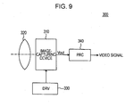
- Fig. 9 shows an example of the configuration of a camera system to which a solid-state image sensor according to an embodiment of the present invention is applied.
- the present camera system 300 includes an image-capturing device 310 to which the solid-state image sensor 10 according to the present embodiment can be applied, an optical system that guides incident light to a pixel area of the image-capturing device 310 (subject image is formed), for example, a lens 320 that forms incident light (image light) into an image on the imaging plane, a driving circuit (DRV) 330 for driving the image-capturing device 310, and a signal processing circuit (PRC) 340 for processing an output signal of the image-capturing device 310.
- an optical system that guides incident light to a pixel area of the image-capturing device 310 (subject image is formed)
- a lens 320 that forms incident light (image light) into an image on the imaging plane
- a driving circuit (DRV) 330 for driving the image-capturing device 310
- PRC signal processing circuit
- the driving circuit 330 has a timing generator (not shown) for generating various kinds of timing signals including a start pulse and a clock pulse with which circuits in the image-capturing device 310 are driven, and drives the image-capturing device 310 in accordance with a predetermined timing signal.
- a timing generator (not shown) for generating various kinds of timing signals including a start pulse and a clock pulse with which circuits in the image-capturing device 310 are driven, and drives the image-capturing device 310 in accordance with a predetermined timing signal.
- the signal processing circuit 340 performs signal processing, such as correlated double sampling (CDS), on the output signal of the image-capturing device 310.
- signal processing such as correlated double sampling (CDS)
- the image signal processed by the signal processing circuit 340 is recorded on, for example, a recording medium, such as a memory.
- the image information recorded on a recording medium is printed in hard copy form by using a printer or the like.
- the image signal processed by the signal processing circuit 340 is displayed as a moving image on a monitor formed of a liquid-crystal display or the like.
- the image sensor 10 described above as the image-capturing device 310 in an image-capturing apparatus, such as a digital still camera, a high-accuracy camera can be realized.
Landscapes
- Engineering & Computer Science (AREA)
- Theoretical Computer Science (AREA)
- Multimedia (AREA)
- Signal Processing (AREA)
- Transforming Light Signals Into Electric Signals (AREA)
- Analogue/Digital Conversion (AREA)
Applications Claiming Priority (2)
| Application Number | Priority Date | Filing Date | Title |
|---|---|---|---|
| JP2007256555A JP4853445B2 (ja) | 2007-09-28 | 2007-09-28 | A/d変換回路、固体撮像素子、およびカメラシステム |
| PCT/JP2008/067253 WO2009041474A1 (ja) | 2007-09-28 | 2008-09-25 | A/d変換回路、固体撮像素子、およびカメラシステム |
Publications (3)
| Publication Number | Publication Date |
|---|---|
| EP2197118A1 EP2197118A1 (en) | 2010-06-16 |
| EP2197118A4 EP2197118A4 (en) | 2012-11-14 |
| EP2197118B1 true EP2197118B1 (en) | 2014-01-15 |
Family
ID=40511357
Family Applications (1)
| Application Number | Title | Priority Date | Filing Date |
|---|---|---|---|
| EP08834294.4A Not-in-force EP2197118B1 (en) | 2007-09-28 | 2008-09-25 | A/d converting circuit, solid-state image sensing device and camera system |
Country Status (7)
| Country | Link |
|---|---|
| US (2) | US8330635B2 (enExample) |
| EP (1) | EP2197118B1 (enExample) |
| JP (1) | JP4853445B2 (enExample) |
| KR (1) | KR101481853B1 (enExample) |
| CN (1) | CN101803199B (enExample) |
| TW (1) | TWI392354B (enExample) |
| WO (1) | WO2009041474A1 (enExample) |
Families Citing this family (42)
| Publication number | Priority date | Publication date | Assignee | Title |
|---|---|---|---|---|
| JP4853445B2 (ja) * | 2007-09-28 | 2012-01-11 | ソニー株式会社 | A/d変換回路、固体撮像素子、およびカメラシステム |
| JP2009159331A (ja) * | 2007-12-26 | 2009-07-16 | Panasonic Corp | 固体撮像装置、その駆動方法およびカメラ |
| JP5254140B2 (ja) * | 2009-07-14 | 2013-08-07 | 株式会社東芝 | A/d変換器及びそれを備えた固体撮像装置 |
| KR101647366B1 (ko) * | 2009-09-25 | 2016-08-11 | 삼성전자주식회사 | 카운터 회로, 이를 포함하는 장치 및 카운팅 방법 |
| JP5619434B2 (ja) * | 2010-02-26 | 2014-11-05 | パナソニック株式会社 | 固体撮像装置および撮像装置 |
| JP5507309B2 (ja) * | 2010-03-30 | 2014-05-28 | 本田技研工業株式会社 | 信号処理方法及び固体撮像装置 |
| KR101211082B1 (ko) | 2010-12-03 | 2012-12-12 | 동국대학교 산학협력단 | 컬럼 고정 패턴 노이즈를 제거하기 위한 adc 및 이를 포함하는 cmos 이미지 센서 |
| KR101758090B1 (ko) * | 2010-12-06 | 2017-07-17 | 삼성전자주식회사 | 이미지 센서 및 이미지 센서를 포함하는 카메라 시스템 |
| JP5631781B2 (ja) * | 2011-03-08 | 2014-11-26 | オリンパス株式会社 | Ad変換回路および撮像装置 |
| JP5784377B2 (ja) * | 2011-06-14 | 2015-09-24 | オリンパス株式会社 | Ad変換回路および撮像装置 |
| JP5808162B2 (ja) * | 2011-06-23 | 2015-11-10 | キヤノン株式会社 | 撮像素子、撮像装置及び撮像素子の駆動方法 |
| JP5854673B2 (ja) | 2011-07-12 | 2016-02-09 | キヤノン株式会社 | 固体撮像装置 |
| JP5659112B2 (ja) * | 2011-09-12 | 2015-01-28 | オリンパス株式会社 | Ad変換回路および撮像装置 |
| US8576979B2 (en) * | 2011-10-11 | 2013-11-05 | Omnivision Technologies, Inc. | Arithmetic counter circuit, configuration and application for high performance CMOS image sensors |
| JP2013255101A (ja) * | 2012-06-07 | 2013-12-19 | Olympus Corp | 撮像装置 |
| JP6019793B2 (ja) | 2012-06-20 | 2016-11-02 | ソニー株式会社 | カウンタ、カウント方法、ad変換装置、固体撮像素子、および電子装置 |
| JP5980080B2 (ja) * | 2012-10-02 | 2016-08-31 | キヤノン株式会社 | 光電変換装置、撮像システム、光電変換装置の検査方法および撮像システムの製造方法 |
| JP5941816B2 (ja) * | 2012-10-04 | 2016-06-29 | オリンパス株式会社 | Ad変換回路および固体撮像装置 |
| JP5990080B2 (ja) * | 2012-10-05 | 2016-09-07 | キヤノン株式会社 | 撮像システム、および撮像システムの駆動方法 |
| GB201300999D0 (en) * | 2013-01-21 | 2013-03-06 | Cmosis Nv | Analog-to-digital conversation in pixel arrays |
| KR101985701B1 (ko) * | 2013-05-20 | 2019-06-04 | 에스케이하이닉스 주식회사 | 비닝 모드 시 전력 소모 감소를 위한 카운팅 장치 및 그 방법 |
| KR102057575B1 (ko) | 2013-07-25 | 2019-12-20 | 삼성전자주식회사 | 이미지 센서 및 그것의 제어 방법 |
| KR102123432B1 (ko) | 2013-11-04 | 2020-06-16 | 삼성전자주식회사 | 카운터 회로 및 이를 포함하는 이미지 센서 |
| US9749555B2 (en) * | 2014-02-04 | 2017-08-29 | Semiconductor Components Industries, Llc | Arithmetic memory with horizontal binning capabilities for imaging systems |
| JP6411795B2 (ja) * | 2014-02-13 | 2018-10-24 | ソニーセミコンダクタソリューションズ株式会社 | 信号処理装置および方法、撮像素子、並びに、撮像装置 |
| KR102230446B1 (ko) * | 2014-07-31 | 2021-03-23 | 에스케이하이닉스 주식회사 | 전자 장치 및 그를 포함하는 전자 시스템 |
| CN107079123B (zh) * | 2014-10-06 | 2021-05-14 | 索尼半导体解决方案公司 | 信号处理装置、信号处理方法、摄像元件和电子设备 |
| DE102015111752B4 (de) * | 2015-07-20 | 2025-11-13 | Infineon Technologies Ag | Verfahren zur verwendung in einem messsystem, sowie messsystem, steuerungseinheit und schnittstelle dazu |
| JP6702821B2 (ja) * | 2016-07-28 | 2020-06-03 | キヤノン株式会社 | 撮像装置及びその制御方法、プログラム、記憶媒体 |
| KR101758602B1 (ko) * | 2016-08-04 | 2017-07-17 | 삼성전자주식회사 | 카운터 회로, 이를 포함하는 장치 및 카운팅 방법 |
| US10191124B2 (en) * | 2016-08-26 | 2019-01-29 | Sii Semiconductor Corporation | Sensor circuit |
| JP6868381B2 (ja) * | 2016-12-09 | 2021-05-12 | ローム株式会社 | 電圧変動検知回路、半導体集積回路、車両 |
| JP6871815B2 (ja) * | 2017-06-30 | 2021-05-12 | キヤノン株式会社 | 撮像装置及びその駆動方法 |
| US10659055B1 (en) * | 2018-11-14 | 2020-05-19 | Omnivision Technologies, Inc. | Two stage gray code counter with a redundant bit |
| KR20210046897A (ko) * | 2019-10-18 | 2021-04-29 | 삼성전자주식회사 | 카운터 회로 및 그것을 포함하는 이미지 센서 |
| JP7463767B2 (ja) * | 2020-03-02 | 2024-04-09 | 株式会社リコー | 受光装置及び距離計測装置 |
| WO2021236021A1 (en) * | 2020-05-22 | 2021-11-25 | Brillnics Singapore Pte. Ltd. | System, method, device and data structure for digital pixel sensors |
| JP7600862B2 (ja) * | 2021-05-25 | 2024-12-17 | 株式会社Jvcケンウッド | コンパレータ回路、及び駆動回路 |
| CN113162609B (zh) * | 2021-05-26 | 2024-06-04 | 中国科学院微电子研究所 | 一种异步计数器 |
| JP2023023877A (ja) * | 2021-08-06 | 2023-02-16 | ブリルニクス シンガポール プライベート リミテッド | 固体撮像装置、固体撮像装置の駆動方法、および電子機器 |
| CN115134548B (zh) * | 2022-06-30 | 2025-11-25 | 上海集成电路装备材料产业创新中心有限公司 | 双沿计数电路、读出电路及图像传感器 |
| CN118381607B (zh) * | 2024-06-21 | 2024-08-20 | 湖北工业大学 | 一种新型静态隐匿的dff-puf复合电路 |
Family Cites Families (24)
| Publication number | Priority date | Publication date | Assignee | Title |
|---|---|---|---|---|
| US4521898A (en) * | 1982-12-28 | 1985-06-04 | Motorola, Inc. | Ripple counter circuit having reduced propagation delay |
| JPH06311025A (ja) * | 1993-04-27 | 1994-11-04 | Oki Micro Design Miyazaki:Kk | アップダウンカウンタ回路 |
| US5887715A (en) * | 1997-08-08 | 1999-03-30 | Maxtech, Inc. | Tool case with snap-in modules |
| US5920274A (en) * | 1997-08-05 | 1999-07-06 | International Business Machines Corporation | Image sensor employing non-uniform A/D conversion |
| EP1001534A2 (en) * | 1998-10-07 | 2000-05-17 | Yozan Inc. | Analog to digital converter |
| US7129883B2 (en) * | 2004-02-23 | 2006-10-31 | Sony Corporation | Method and apparatus for AD conversion, semiconductor device for detecting distribution of physical quantity, and electronic apparatus |
| JP4470700B2 (ja) | 2004-02-23 | 2010-06-02 | ソニー株式会社 | Ad変換方法およびad変換装置並びに物理量分布検知の半導体装置および電子機器 |
| JP4107269B2 (ja) * | 2004-02-23 | 2008-06-25 | ソニー株式会社 | 固体撮像装置 |
| JP4655500B2 (ja) | 2004-04-12 | 2011-03-23 | ソニー株式会社 | Ad変換装置並びに物理量分布検知の半導体装置および電子機器 |
| JP4289206B2 (ja) * | 2004-04-26 | 2009-07-01 | ソニー株式会社 | カウンタ回路 |
| JP2005313331A (ja) * | 2004-04-27 | 2005-11-10 | Ricoh Co Ltd | 位置情報の異常対策手段を備えた記録装置 |
| DE602005013469D1 (de) | 2004-11-08 | 2009-05-07 | Sony Corp | Verfahren zur Analog-Digital-Wandlung, Analog-Digital-Wandler, Halbleitervorrichtung zur Detektierung der Verteilung von physikalischen Grössen und elektronisches Gerät |
| JP4442515B2 (ja) * | 2005-06-02 | 2010-03-31 | ソニー株式会社 | 固体撮像装置、固体撮像装置におけるアナログ−デジタル変換方法および撮像装置 |
| JP4524652B2 (ja) * | 2005-07-06 | 2010-08-18 | ソニー株式会社 | Ad変換装置並びに半導体装置 |
| KR100723517B1 (ko) * | 2005-12-14 | 2007-05-30 | 삼성전자주식회사 | 카운팅 값을 유지한 후 출력하는 카운터 및 상기 카운터를 구비하는 위상 고정 루프 |
| JP4615472B2 (ja) * | 2006-04-03 | 2011-01-19 | ソニー株式会社 | 物理量分布検出装置および撮像装置 |
| JP5076568B2 (ja) * | 2007-03-12 | 2012-11-21 | ソニー株式会社 | データ処理方法、データ処理装置、固体撮像装置、撮像装置、電子機器 |
| JP4853445B2 (ja) * | 2007-09-28 | 2012-01-11 | ソニー株式会社 | A/d変換回路、固体撮像素子、およびカメラシステム |
| JP4946761B2 (ja) * | 2007-09-28 | 2012-06-06 | ソニー株式会社 | 固体撮像素子およびカメラシステム |
| JP2009159331A (ja) * | 2007-12-26 | 2009-07-16 | Panasonic Corp | 固体撮像装置、その駆動方法およびカメラ |
| JP5347341B2 (ja) * | 2008-06-06 | 2013-11-20 | ソニー株式会社 | 固体撮像装置、撮像装置、電子機器、ad変換装置、ad変換方法 |
| KR101621244B1 (ko) * | 2009-02-13 | 2016-05-16 | 삼성전자주식회사 | 카운터 회로, 이를 포함하는 장치 및 카운팅 방법 |
| KR101365408B1 (ko) * | 2009-03-03 | 2014-02-19 | 삼성전자주식회사 | 카운터 회로, 이를 포함하는 물리량 측정 장치 및 카운팅 방법 |
| JP5251778B2 (ja) * | 2009-08-03 | 2013-07-31 | ソニー株式会社 | 固体撮像装置、固体撮像装置のアナログ−デジタル変換方法および電子機器 |
-
2007
- 2007-09-28 JP JP2007256555A patent/JP4853445B2/ja not_active Expired - Fee Related
-
2008
- 2008-09-25 WO PCT/JP2008/067253 patent/WO2009041474A1/ja not_active Ceased
- 2008-09-25 EP EP08834294.4A patent/EP2197118B1/en not_active Not-in-force
- 2008-09-25 KR KR1020107006083A patent/KR101481853B1/ko not_active Expired - Fee Related
- 2008-09-25 CN CN200880107809.7A patent/CN101803199B/zh not_active Expired - Fee Related
- 2008-09-25 US US12/678,807 patent/US8330635B2/en not_active Expired - Fee Related
- 2008-09-26 TW TW097137293A patent/TWI392354B/zh not_active IP Right Cessation
-
2012
- 2012-11-08 US US13/672,252 patent/US8981983B2/en active Active
Also Published As
| Publication number | Publication date |
|---|---|
| EP2197118A4 (en) | 2012-11-14 |
| JP2009089066A (ja) | 2009-04-23 |
| US20130147999A1 (en) | 2013-06-13 |
| US8330635B2 (en) | 2012-12-11 |
| KR20100072199A (ko) | 2010-06-30 |
| US20100194949A1 (en) | 2010-08-05 |
| KR101481853B1 (ko) | 2015-01-12 |
| JP4853445B2 (ja) | 2012-01-11 |
| WO2009041474A1 (ja) | 2009-04-02 |
| TW200922310A (en) | 2009-05-16 |
| CN101803199A (zh) | 2010-08-11 |
| US8981983B2 (en) | 2015-03-17 |
| EP2197118A1 (en) | 2010-06-16 |
| CN101803199B (zh) | 2013-08-28 |
| TWI392354B (zh) | 2013-04-01 |
Similar Documents
| Publication | Publication Date | Title |
|---|---|---|
| EP2197118B1 (en) | A/d converting circuit, solid-state image sensing device and camera system | |
| CN101826867B (zh) | 计数器、模数转换方法和转换器、半导体器件及电子装置 | |
| US8130295B2 (en) | Analog-to-digital converter, solid-state image pickup device, and camera system | |
| EP1655840B1 (en) | Analog-to-digital conversion method, analog-to-digital converter, semiconductor device for detecting distribution of physical quantity, and electronic apparatus | |
| US9871986B2 (en) | Counter, counting method, ad converter, solid-state imaging device, and electronic device | |
| JP2012165168A (ja) | 半導体装置、物理情報取得装置、及び、信号読出し方法 | |
| JP4743227B2 (ja) | Ad変換方法およびad変換装置、並びに物理量分布検知の半導体装置および電子機器 | |
| JP2009038781A (ja) | 固体撮像装置、固体撮像装置のアナログ−デジタル変換方法および撮像装置 | |
| JP4978795B2 (ja) | 固体撮像装置、駆動制御方法、および撮像装置 | |
| JP5234157B2 (ja) | A/d変換方法およびカメラシステム |
Legal Events
| Date | Code | Title | Description |
|---|---|---|---|
| PUAI | Public reference made under article 153(3) epc to a published international application that has entered the european phase |
Free format text: ORIGINAL CODE: 0009012 |
|
| 17P | Request for examination filed |
Effective date: 20100319 |
|
| AK | Designated contracting states |
Kind code of ref document: A1 Designated state(s): AT BE BG CH CY CZ DE DK EE ES FI FR GB GR HR HU IE IS IT LI LT LU LV MC MT NL NO PL PT RO SE SI SK TR |
|
| AX | Request for extension of the european patent |
Extension state: AL BA MK RS |
|
| DAX | Request for extension of the european patent (deleted) | ||
| A4 | Supplementary search report drawn up and despatched |
Effective date: 20121017 |
|
| RIC1 | Information provided on ipc code assigned before grant |
Ipc: H03K 23/62 20060101ALI20121011BHEP Ipc: H03M 1/12 20060101ALI20121011BHEP Ipc: H04N 5/335 20110101ALI20121011BHEP Ipc: H01L 27/148 20060101ALI20121011BHEP Ipc: H03M 1/10 20060101ALI20121011BHEP Ipc: H04N 5/378 20110101ALI20121011BHEP Ipc: H03M 1/20 20060101ALI20121011BHEP Ipc: H03M 1/56 20060101AFI20121011BHEP |
|
| GRAP | Despatch of communication of intention to grant a patent |
Free format text: ORIGINAL CODE: EPIDOSNIGR1 |
|
| INTG | Intention to grant announced |
Effective date: 20130808 |
|
| GRAS | Grant fee paid |
Free format text: ORIGINAL CODE: EPIDOSNIGR3 |
|
| GRAA | (expected) grant |
Free format text: ORIGINAL CODE: 0009210 |
|
| AK | Designated contracting states |
Kind code of ref document: B1 Designated state(s): AT BE BG CH CY CZ DE DK EE ES FI FR GB GR HR HU IE IS IT LI LT LU LV MC MT NL NO PL PT RO SE SI SK TR |
|
| REG | Reference to a national code |
Ref country code: CH Ref legal event code: EP Ref country code: GB Ref legal event code: FG4D |
|
| REG | Reference to a national code |
Ref country code: AT Ref legal event code: REF Ref document number: 650206 Country of ref document: AT Kind code of ref document: T Effective date: 20140215 |
|
| REG | Reference to a national code |
Ref country code: IE Ref legal event code: FG4D |
|
| REG | Reference to a national code |
Ref country code: DE Ref legal event code: R096 Ref document number: 602008029981 Country of ref document: DE Effective date: 20140227 |
|
| REG | Reference to a national code |
Ref country code: NL Ref legal event code: VDEP Effective date: 20140115 |
|
| REG | Reference to a national code |
Ref country code: AT Ref legal event code: MK05 Ref document number: 650206 Country of ref document: AT Kind code of ref document: T Effective date: 20140115 |
|
| REG | Reference to a national code |
Ref country code: LT Ref legal event code: MG4D |
|
| PG25 | Lapsed in a contracting state [announced via postgrant information from national office to epo] |
Ref country code: NO Free format text: LAPSE BECAUSE OF FAILURE TO SUBMIT A TRANSLATION OF THE DESCRIPTION OR TO PAY THE FEE WITHIN THE PRESCRIBED TIME-LIMIT Effective date: 20140415 Ref country code: IS Free format text: LAPSE BECAUSE OF FAILURE TO SUBMIT A TRANSLATION OF THE DESCRIPTION OR TO PAY THE FEE WITHIN THE PRESCRIBED TIME-LIMIT Effective date: 20140515 Ref country code: LT Free format text: LAPSE BECAUSE OF FAILURE TO SUBMIT A TRANSLATION OF THE DESCRIPTION OR TO PAY THE FEE WITHIN THE PRESCRIBED TIME-LIMIT Effective date: 20140115 |
|
| PG25 | Lapsed in a contracting state [announced via postgrant information from national office to epo] |
Ref country code: SE Free format text: LAPSE BECAUSE OF FAILURE TO SUBMIT A TRANSLATION OF THE DESCRIPTION OR TO PAY THE FEE WITHIN THE PRESCRIBED TIME-LIMIT Effective date: 20140115 Ref country code: CY Free format text: LAPSE BECAUSE OF FAILURE TO SUBMIT A TRANSLATION OF THE DESCRIPTION OR TO PAY THE FEE WITHIN THE PRESCRIBED TIME-LIMIT Effective date: 20140115 Ref country code: AT Free format text: LAPSE BECAUSE OF FAILURE TO SUBMIT A TRANSLATION OF THE DESCRIPTION OR TO PAY THE FEE WITHIN THE PRESCRIBED TIME-LIMIT Effective date: 20140115 Ref country code: PT Free format text: LAPSE BECAUSE OF FAILURE TO SUBMIT A TRANSLATION OF THE DESCRIPTION OR TO PAY THE FEE WITHIN THE PRESCRIBED TIME-LIMIT Effective date: 20140515 Ref country code: NL Free format text: LAPSE BECAUSE OF FAILURE TO SUBMIT A TRANSLATION OF THE DESCRIPTION OR TO PAY THE FEE WITHIN THE PRESCRIBED TIME-LIMIT Effective date: 20140115 Ref country code: ES Free format text: LAPSE BECAUSE OF FAILURE TO SUBMIT A TRANSLATION OF THE DESCRIPTION OR TO PAY THE FEE WITHIN THE PRESCRIBED TIME-LIMIT Effective date: 20140115 Ref country code: FI Free format text: LAPSE BECAUSE OF FAILURE TO SUBMIT A TRANSLATION OF THE DESCRIPTION OR TO PAY THE FEE WITHIN THE PRESCRIBED TIME-LIMIT Effective date: 20140115 |
|
| PG25 | Lapsed in a contracting state [announced via postgrant information from national office to epo] |
Ref country code: HR Free format text: LAPSE BECAUSE OF FAILURE TO SUBMIT A TRANSLATION OF THE DESCRIPTION OR TO PAY THE FEE WITHIN THE PRESCRIBED TIME-LIMIT Effective date: 20140115 Ref country code: LV Free format text: LAPSE BECAUSE OF FAILURE TO SUBMIT A TRANSLATION OF THE DESCRIPTION OR TO PAY THE FEE WITHIN THE PRESCRIBED TIME-LIMIT Effective date: 20140115 Ref country code: BE Free format text: LAPSE BECAUSE OF FAILURE TO SUBMIT A TRANSLATION OF THE DESCRIPTION OR TO PAY THE FEE WITHIN THE PRESCRIBED TIME-LIMIT Effective date: 20140115 |
|
| REG | Reference to a national code |
Ref country code: DE Ref legal event code: R097 Ref document number: 602008029981 Country of ref document: DE |
|
| PG25 | Lapsed in a contracting state [announced via postgrant information from national office to epo] |
Ref country code: EE Free format text: LAPSE BECAUSE OF FAILURE TO SUBMIT A TRANSLATION OF THE DESCRIPTION OR TO PAY THE FEE WITHIN THE PRESCRIBED TIME-LIMIT Effective date: 20140115 Ref country code: DK Free format text: LAPSE BECAUSE OF FAILURE TO SUBMIT A TRANSLATION OF THE DESCRIPTION OR TO PAY THE FEE WITHIN THE PRESCRIBED TIME-LIMIT Effective date: 20140115 Ref country code: RO Free format text: LAPSE BECAUSE OF FAILURE TO SUBMIT A TRANSLATION OF THE DESCRIPTION OR TO PAY THE FEE WITHIN THE PRESCRIBED TIME-LIMIT Effective date: 20140115 Ref country code: CZ Free format text: LAPSE BECAUSE OF FAILURE TO SUBMIT A TRANSLATION OF THE DESCRIPTION OR TO PAY THE FEE WITHIN THE PRESCRIBED TIME-LIMIT Effective date: 20140115 |
|
| PLBE | No opposition filed within time limit |
Free format text: ORIGINAL CODE: 0009261 |
|
| STAA | Information on the status of an ep patent application or granted ep patent |
Free format text: STATUS: NO OPPOSITION FILED WITHIN TIME LIMIT |
|
| PG25 | Lapsed in a contracting state [announced via postgrant information from national office to epo] |
Ref country code: SK Free format text: LAPSE BECAUSE OF FAILURE TO SUBMIT A TRANSLATION OF THE DESCRIPTION OR TO PAY THE FEE WITHIN THE PRESCRIBED TIME-LIMIT Effective date: 20140115 Ref country code: PL Free format text: LAPSE BECAUSE OF FAILURE TO SUBMIT A TRANSLATION OF THE DESCRIPTION OR TO PAY THE FEE WITHIN THE PRESCRIBED TIME-LIMIT Effective date: 20140115 |
|
| PGFP | Annual fee paid to national office [announced via postgrant information from national office to epo] |
Ref country code: GB Payment date: 20140919 Year of fee payment: 7 Ref country code: FR Payment date: 20140919 Year of fee payment: 7 |
|
| 26N | No opposition filed |
Effective date: 20141016 |
|
| REG | Reference to a national code |
Ref country code: DE Ref legal event code: R097 Ref document number: 602008029981 Country of ref document: DE Effective date: 20141016 |
|
| PG25 | Lapsed in a contracting state [announced via postgrant information from national office to epo] |
Ref country code: LU Free format text: LAPSE BECAUSE OF FAILURE TO SUBMIT A TRANSLATION OF THE DESCRIPTION OR TO PAY THE FEE WITHIN THE PRESCRIBED TIME-LIMIT Effective date: 20140925 Ref country code: MC Free format text: LAPSE BECAUSE OF FAILURE TO SUBMIT A TRANSLATION OF THE DESCRIPTION OR TO PAY THE FEE WITHIN THE PRESCRIBED TIME-LIMIT Effective date: 20140115 |
|
| REG | Reference to a national code |
Ref country code: CH Ref legal event code: PL |
|
| PG25 | Lapsed in a contracting state [announced via postgrant information from national office to epo] |
Ref country code: SI Free format text: LAPSE BECAUSE OF FAILURE TO SUBMIT A TRANSLATION OF THE DESCRIPTION OR TO PAY THE FEE WITHIN THE PRESCRIBED TIME-LIMIT Effective date: 20140115 |
|
| REG | Reference to a national code |
Ref country code: IE Ref legal event code: MM4A |
|
| PG25 | Lapsed in a contracting state [announced via postgrant information from national office to epo] |
Ref country code: CH Free format text: LAPSE BECAUSE OF NON-PAYMENT OF DUE FEES Effective date: 20140930 Ref country code: LI Free format text: LAPSE BECAUSE OF NON-PAYMENT OF DUE FEES Effective date: 20140930 |
|
| PG25 | Lapsed in a contracting state [announced via postgrant information from national office to epo] |
Ref country code: IE Free format text: LAPSE BECAUSE OF NON-PAYMENT OF DUE FEES Effective date: 20140925 |
|
| GBPC | Gb: european patent ceased through non-payment of renewal fee |
Effective date: 20150925 |
|
| PG25 | Lapsed in a contracting state [announced via postgrant information from national office to epo] |
Ref country code: BG Free format text: LAPSE BECAUSE OF FAILURE TO SUBMIT A TRANSLATION OF THE DESCRIPTION OR TO PAY THE FEE WITHIN THE PRESCRIBED TIME-LIMIT Effective date: 20140115 |
|
| PG25 | Lapsed in a contracting state [announced via postgrant information from national office to epo] |
Ref country code: GR Free format text: LAPSE BECAUSE OF FAILURE TO SUBMIT A TRANSLATION OF THE DESCRIPTION OR TO PAY THE FEE WITHIN THE PRESCRIBED TIME-LIMIT Effective date: 20140416 Ref country code: MT Free format text: LAPSE BECAUSE OF FAILURE TO SUBMIT A TRANSLATION OF THE DESCRIPTION OR TO PAY THE FEE WITHIN THE PRESCRIBED TIME-LIMIT Effective date: 20140115 Ref country code: IT Free format text: LAPSE BECAUSE OF FAILURE TO SUBMIT A TRANSLATION OF THE DESCRIPTION OR TO PAY THE FEE WITHIN THE PRESCRIBED TIME-LIMIT Effective date: 20140115 |
|
| REG | Reference to a national code |
Ref country code: FR Ref legal event code: ST Effective date: 20160531 |
|
| PG25 | Lapsed in a contracting state [announced via postgrant information from national office to epo] |
Ref country code: HU Free format text: LAPSE BECAUSE OF FAILURE TO SUBMIT A TRANSLATION OF THE DESCRIPTION OR TO PAY THE FEE WITHIN THE PRESCRIBED TIME-LIMIT; INVALID AB INITIO Effective date: 20080925 Ref country code: TR Free format text: LAPSE BECAUSE OF FAILURE TO SUBMIT A TRANSLATION OF THE DESCRIPTION OR TO PAY THE FEE WITHIN THE PRESCRIBED TIME-LIMIT Effective date: 20140115 Ref country code: GB Free format text: LAPSE BECAUSE OF NON-PAYMENT OF DUE FEES Effective date: 20150925 |
|
| PG25 | Lapsed in a contracting state [announced via postgrant information from national office to epo] |
Ref country code: FR Free format text: LAPSE BECAUSE OF NON-PAYMENT OF DUE FEES Effective date: 20150930 |
|
| PGFP | Annual fee paid to national office [announced via postgrant information from national office to epo] |
Ref country code: DE Payment date: 20220616 Year of fee payment: 15 |
|
| P01 | Opt-out of the competence of the unified patent court (upc) registered |
Effective date: 20230527 |
|
| REG | Reference to a national code |
Ref country code: DE Ref legal event code: R119 Ref document number: 602008029981 Country of ref document: DE |
|
| PG25 | Lapsed in a contracting state [announced via postgrant information from national office to epo] |
Ref country code: DE Free format text: LAPSE BECAUSE OF NON-PAYMENT OF DUE FEES Effective date: 20240403 |