EP2133448B1 - Verfahren und vorrichtung zur herstellung einer oberflächenaufgerauhten kupferplatte - Google Patents
Verfahren und vorrichtung zur herstellung einer oberflächenaufgerauhten kupferplatte Download PDFInfo
- Publication number
- EP2133448B1 EP2133448B1 EP08721206.4A EP08721206A EP2133448B1 EP 2133448 B1 EP2133448 B1 EP 2133448B1 EP 08721206 A EP08721206 A EP 08721206A EP 2133448 B1 EP2133448 B1 EP 2133448B1
- Authority
- EP
- European Patent Office
- Prior art keywords
- copper
- copper plate
- therefor
- electrodes
- plate
- Prior art date
- Legal status (The legal status is an assumption and is not a legal conclusion. Google has not performed a legal analysis and makes no representation as to the accuracy of the status listed.)
- Active
Links
- RYGMFSIKBFXOCR-UHFFFAOYSA-N Copper Chemical compound [Cu] RYGMFSIKBFXOCR-UHFFFAOYSA-N 0.000 title claims description 405
- 229910052802 copper Inorganic materials 0.000 title claims description 379
- 239000010949 copper Substances 0.000 title claims description 379
- 238000007788 roughening Methods 0.000 title description 18
- 238000004519 manufacturing process Methods 0.000 title description 2
- 238000011282 treatment Methods 0.000 claims description 158
- 238000000034 method Methods 0.000 claims description 146
- 238000007747 plating Methods 0.000 claims description 64
- 238000009713 electroplating Methods 0.000 claims description 50
- 229910052751 metal Inorganic materials 0.000 claims description 49
- 239000002184 metal Substances 0.000 claims description 49
- 239000010419 fine particle Substances 0.000 claims description 23
- 230000008878 coupling Effects 0.000 claims 1
- 238000010168 coupling process Methods 0.000 claims 1
- 238000005859 coupling reaction Methods 0.000 claims 1
- 239000000758 substrate Substances 0.000 description 41
- 239000011889 copper foil Substances 0.000 description 16
- 230000003746 surface roughness Effects 0.000 description 16
- 238000012545 processing Methods 0.000 description 15
- 230000000052 comparative effect Effects 0.000 description 14
- 229920000298 Cellophane Polymers 0.000 description 13
- 239000003795 chemical substances by application Substances 0.000 description 11
- 238000012360 testing method Methods 0.000 description 11
- 238000005259 measurement Methods 0.000 description 10
- 239000000126 substance Substances 0.000 description 10
- 239000011888 foil Substances 0.000 description 9
- QAOWNCQODCNURD-UHFFFAOYSA-N Sulfuric acid Chemical compound OS(O)(=O)=O QAOWNCQODCNURD-UHFFFAOYSA-N 0.000 description 8
- 238000004026 adhesive bonding Methods 0.000 description 8
- 239000002245 particle Substances 0.000 description 8
- 229910000679 solder Inorganic materials 0.000 description 8
- 239000011347 resin Substances 0.000 description 7
- 229920005989 resin Polymers 0.000 description 7
- 238000005406 washing Methods 0.000 description 7
- VEXZGXHMUGYJMC-UHFFFAOYSA-N Hydrochloric acid Chemical compound Cl VEXZGXHMUGYJMC-UHFFFAOYSA-N 0.000 description 6
- 239000000853 adhesive Substances 0.000 description 6
- 230000001070 adhesive effect Effects 0.000 description 6
- 238000010438 heat treatment Methods 0.000 description 6
- 150000002500 ions Chemical class 0.000 description 6
- 239000000463 material Substances 0.000 description 6
- BASFCYQUMIYNBI-UHFFFAOYSA-N platinum Chemical compound [Pt] BASFCYQUMIYNBI-UHFFFAOYSA-N 0.000 description 6
- 238000003825 pressing Methods 0.000 description 6
- XLYOFNOQVPJJNP-UHFFFAOYSA-N water Substances O XLYOFNOQVPJJNP-UHFFFAOYSA-N 0.000 description 6
- 238000005282 brightening Methods 0.000 description 5
- 238000005553 drilling Methods 0.000 description 5
- 238000002474 experimental method Methods 0.000 description 5
- 238000005554 pickling Methods 0.000 description 5
- RTAQQCXQSZGOHL-UHFFFAOYSA-N Titanium Chemical compound [Ti] RTAQQCXQSZGOHL-UHFFFAOYSA-N 0.000 description 4
- 238000004140 cleaning Methods 0.000 description 4
- 238000013461 design Methods 0.000 description 4
- 230000006866 deterioration Effects 0.000 description 4
- 238000005530 etching Methods 0.000 description 4
- 239000000047 product Substances 0.000 description 4
- 239000010936 titanium Substances 0.000 description 4
- 229910052719 titanium Inorganic materials 0.000 description 4
- 229910000881 Cu alloy Inorganic materials 0.000 description 3
- 229910000831 Steel Inorganic materials 0.000 description 3
- QAOWNCQODCNURD-UHFFFAOYSA-L Sulfate Chemical compound [O-]S([O-])(=O)=O QAOWNCQODCNURD-UHFFFAOYSA-L 0.000 description 3
- 239000002253 acid Substances 0.000 description 3
- 230000000694 effects Effects 0.000 description 3
- 239000003792 electrolyte Substances 0.000 description 3
- 230000001965 increasing effect Effects 0.000 description 3
- JEIPFZHSYJVQDO-UHFFFAOYSA-N iron(III) oxide Inorganic materials O=[Fe]O[Fe]=O JEIPFZHSYJVQDO-UHFFFAOYSA-N 0.000 description 3
- 229910052697 platinum Inorganic materials 0.000 description 3
- 230000002265 prevention Effects 0.000 description 3
- 239000010959 steel Substances 0.000 description 3
- JPVYNHNXODAKFH-UHFFFAOYSA-N Cu2+ Chemical compound [Cu+2] JPVYNHNXODAKFH-UHFFFAOYSA-N 0.000 description 2
- 239000004593 Epoxy Substances 0.000 description 2
- 239000000654 additive Substances 0.000 description 2
- 230000000996 additive effect Effects 0.000 description 2
- 239000000956 alloy Substances 0.000 description 2
- 238000004873 anchoring Methods 0.000 description 2
- -1 borate ions Chemical class 0.000 description 2
- 229910001430 chromium ion Inorganic materials 0.000 description 2
- JOPOVCBBYLSVDA-UHFFFAOYSA-N chromium(6+) Chemical compound [Cr+6] JOPOVCBBYLSVDA-UHFFFAOYSA-N 0.000 description 2
- 150000001875 compounds Chemical class 0.000 description 2
- 229910001431 copper ion Inorganic materials 0.000 description 2
- 238000004090 dissolution Methods 0.000 description 2
- 238000005868 electrolysis reaction Methods 0.000 description 2
- 230000002708 enhancing effect Effects 0.000 description 2
- 230000017525 heat dissipation Effects 0.000 description 2
- 239000005340 laminated glass Substances 0.000 description 2
- 229910001092 metal group alloy Inorganic materials 0.000 description 2
- 239000000203 mixture Substances 0.000 description 2
- 238000004080 punching Methods 0.000 description 2
- 230000000452 restraining effect Effects 0.000 description 2
- 229910000838 Al alloy Inorganic materials 0.000 description 1
- QPLDLSVMHZLSFG-UHFFFAOYSA-N Copper oxide Chemical compound [Cu]=O QPLDLSVMHZLSFG-UHFFFAOYSA-N 0.000 description 1
- 239000005751 Copper oxide Substances 0.000 description 1
- 241000219094 Vitaceae Species 0.000 description 1
- 230000002159 abnormal effect Effects 0.000 description 1
- 229910052782 aluminium Inorganic materials 0.000 description 1
- XAGFODPZIPBFFR-UHFFFAOYSA-N aluminium Chemical compound [Al] XAGFODPZIPBFFR-UHFFFAOYSA-N 0.000 description 1
- 230000033228 biological regulation Effects 0.000 description 1
- 230000005587 bubbling Effects 0.000 description 1
- 238000006243 chemical reaction Methods 0.000 description 1
- 239000011248 coating agent Substances 0.000 description 1
- 238000000576 coating method Methods 0.000 description 1
- 239000013065 commercial product Substances 0.000 description 1
- 150000001879 copper Chemical class 0.000 description 1
- 229910000431 copper oxide Inorganic materials 0.000 description 1
- 229910000365 copper sulfate Inorganic materials 0.000 description 1
- BERDEBHAJNAUOM-UHFFFAOYSA-N copper(I) oxide Inorganic materials [Cu]O[Cu] BERDEBHAJNAUOM-UHFFFAOYSA-N 0.000 description 1
- ARUVKPQLZAKDPS-UHFFFAOYSA-L copper(II) sulfate Chemical compound [Cu+2].[O-][S+2]([O-])([O-])[O-] ARUVKPQLZAKDPS-UHFFFAOYSA-L 0.000 description 1
- BQJTUDIVKSVBDU-UHFFFAOYSA-L copper;sulfuric acid;sulfate Chemical compound [Cu+2].OS(O)(=O)=O.[O-]S([O-])(=O)=O BQJTUDIVKSVBDU-UHFFFAOYSA-L 0.000 description 1
- KRFJLUBVMFXRPN-UHFFFAOYSA-N cuprous oxide Chemical compound [O-2].[Cu+].[Cu+] KRFJLUBVMFXRPN-UHFFFAOYSA-N 0.000 description 1
- 229940112669 cuprous oxide Drugs 0.000 description 1
- 230000003247 decreasing effect Effects 0.000 description 1
- 238000009792 diffusion process Methods 0.000 description 1
- 238000009429 electrical wiring Methods 0.000 description 1
- 230000007613 environmental effect Effects 0.000 description 1
- 239000012467 final product Substances 0.000 description 1
- 239000011521 glass Substances 0.000 description 1
- 235000021021 grapes Nutrition 0.000 description 1
- 238000007731 hot pressing Methods 0.000 description 1
- 238000002513 implantation Methods 0.000 description 1
- 238000009413 insulation Methods 0.000 description 1
- 238000010030 laminating Methods 0.000 description 1
- 230000014759 maintenance of location Effects 0.000 description 1
- 229910044991 metal oxide Inorganic materials 0.000 description 1
- 150000004706 metal oxides Chemical class 0.000 description 1
- 125000001477 organic nitrogen group Chemical group 0.000 description 1
- 230000003647 oxidation Effects 0.000 description 1
- 238000007254 oxidation reaction Methods 0.000 description 1
- 230000002093 peripheral effect Effects 0.000 description 1
- 238000005096 rolling process Methods 0.000 description 1
- 238000002791 soaking Methods 0.000 description 1
- 238000005476 soldering Methods 0.000 description 1
- 239000002904 solvent Substances 0.000 description 1
Images


Classifications
-
- C—CHEMISTRY; METALLURGY
- C25—ELECTROLYTIC OR ELECTROPHORETIC PROCESSES; APPARATUS THEREFOR
- C25D—PROCESSES FOR THE ELECTROLYTIC OR ELECTROPHORETIC PRODUCTION OF COATINGS; ELECTROFORMING; APPARATUS THEREFOR
- C25D5/00—Electroplating characterised by the process; Pretreatment or after-treatment of workpieces
- C25D5/60—Electroplating characterised by the structure or texture of the layers
- C25D5/615—Microstructure of the layers, e.g. mixed structure
- C25D5/617—Crystalline layers
-
- C—CHEMISTRY; METALLURGY
- C25—ELECTROLYTIC OR ELECTROPHORETIC PROCESSES; APPARATUS THEREFOR
- C25D—PROCESSES FOR THE ELECTROLYTIC OR ELECTROPHORETIC PRODUCTION OF COATINGS; ELECTROFORMING; APPARATUS THEREFOR
- C25D17/00—Constructional parts, or assemblies thereof, of cells for electrolytic coating
-
- C—CHEMISTRY; METALLURGY
- C25—ELECTROLYTIC OR ELECTROPHORETIC PROCESSES; APPARATUS THEREFOR
- C25D—PROCESSES FOR THE ELECTROLYTIC OR ELECTROPHORETIC PRODUCTION OF COATINGS; ELECTROFORMING; APPARATUS THEREFOR
- C25D5/00—Electroplating characterised by the process; Pretreatment or after-treatment of workpieces
- C25D5/02—Electroplating of selected surface areas
-
- C—CHEMISTRY; METALLURGY
- C25—ELECTROLYTIC OR ELECTROPHORETIC PROCESSES; APPARATUS THEREFOR
- C25D—PROCESSES FOR THE ELECTROLYTIC OR ELECTROPHORETIC PRODUCTION OF COATINGS; ELECTROFORMING; APPARATUS THEREFOR
- C25D5/00—Electroplating characterised by the process; Pretreatment or after-treatment of workpieces
- C25D5/10—Electroplating with more than one layer of the same or of different metals
-
- C—CHEMISTRY; METALLURGY
- C25—ELECTROLYTIC OR ELECTROPHORETIC PROCESSES; APPARATUS THEREFOR
- C25D—PROCESSES FOR THE ELECTROLYTIC OR ELECTROPHORETIC PRODUCTION OF COATINGS; ELECTROFORMING; APPARATUS THEREFOR
- C25D5/00—Electroplating characterised by the process; Pretreatment or after-treatment of workpieces
- C25D5/34—Pretreatment of metallic surfaces to be electroplated
-
- C—CHEMISTRY; METALLURGY
- C25—ELECTROLYTIC OR ELECTROPHORETIC PROCESSES; APPARATUS THEREFOR
- C25D—PROCESSES FOR THE ELECTROLYTIC OR ELECTROPHORETIC PRODUCTION OF COATINGS; ELECTROFORMING; APPARATUS THEREFOR
- C25D5/00—Electroplating characterised by the process; Pretreatment or after-treatment of workpieces
- C25D5/48—After-treatment of electroplated surfaces
-
- C—CHEMISTRY; METALLURGY
- C25—ELECTROLYTIC OR ELECTROPHORETIC PROCESSES; APPARATUS THEREFOR
- C25D—PROCESSES FOR THE ELECTROLYTIC OR ELECTROPHORETIC PRODUCTION OF COATINGS; ELECTROFORMING; APPARATUS THEREFOR
- C25D5/00—Electroplating characterised by the process; Pretreatment or after-treatment of workpieces
- C25D5/60—Electroplating characterised by the structure or texture of the layers
- C25D5/605—Surface topography of the layers, e.g. rough, dendritic or nodular layers
-
- C—CHEMISTRY; METALLURGY
- C25—ELECTROLYTIC OR ELECTROPHORETIC PROCESSES; APPARATUS THEREFOR
- C25D—PROCESSES FOR THE ELECTROLYTIC OR ELECTROPHORETIC PRODUCTION OF COATINGS; ELECTROFORMING; APPARATUS THEREFOR
- C25D7/00—Electroplating characterised by the article coated
-
- C—CHEMISTRY; METALLURGY
- C25—ELECTROLYTIC OR ELECTROPHORETIC PROCESSES; APPARATUS THEREFOR
- C25F—PROCESSES FOR THE ELECTROLYTIC REMOVAL OF MATERIALS FROM OBJECTS; APPARATUS THEREFOR
- C25F3/00—Electrolytic etching or polishing
- C25F3/02—Etching
-
- H—ELECTRICITY
- H05—ELECTRIC TECHNIQUES NOT OTHERWISE PROVIDED FOR
- H05K—PRINTED CIRCUITS; CASINGS OR CONSTRUCTIONAL DETAILS OF ELECTRIC APPARATUS; MANUFACTURE OF ASSEMBLAGES OF ELECTRICAL COMPONENTS
- H05K3/00—Apparatus or processes for manufacturing printed circuits
- H05K3/0085—Apparatus for treatments of printed circuits with liquids not provided for in groups H05K3/02 - H05K3/46; conveyors and holding means therefor
-
- H—ELECTRICITY
- H05—ELECTRIC TECHNIQUES NOT OTHERWISE PROVIDED FOR
- H05K—PRINTED CIRCUITS; CASINGS OR CONSTRUCTIONAL DETAILS OF ELECTRIC APPARATUS; MANUFACTURE OF ASSEMBLAGES OF ELECTRICAL COMPONENTS
- H05K3/00—Apparatus or processes for manufacturing printed circuits
- H05K3/38—Improvement of the adhesion between the insulating substrate and the metal
- H05K3/382—Improvement of the adhesion between the insulating substrate and the metal by special treatment of the metal
- H05K3/384—Improvement of the adhesion between the insulating substrate and the metal by special treatment of the metal by plating
-
- C—CHEMISTRY; METALLURGY
- C25—ELECTROLYTIC OR ELECTROPHORETIC PROCESSES; APPARATUS THEREFOR
- C25D—PROCESSES FOR THE ELECTROLYTIC OR ELECTROPHORETIC PRODUCTION OF COATINGS; ELECTROFORMING; APPARATUS THEREFOR
- C25D3/00—Electroplating: Baths therefor
- C25D3/02—Electroplating: Baths therefor from solutions
- C25D3/38—Electroplating: Baths therefor from solutions of copper
-
- H—ELECTRICITY
- H05—ELECTRIC TECHNIQUES NOT OTHERWISE PROVIDED FOR
- H05K—PRINTED CIRCUITS; CASINGS OR CONSTRUCTIONAL DETAILS OF ELECTRIC APPARATUS; MANUFACTURE OF ASSEMBLAGES OF ELECTRICAL COMPONENTS
- H05K1/00—Printed circuits
- H05K1/02—Details
- H05K1/03—Use of materials for the substrate
- H05K1/05—Insulated conductive substrates, e.g. insulated metal substrate
- H05K1/056—Insulated conductive substrates, e.g. insulated metal substrate the metal substrate being covered by an organic insulating layer
-
- H—ELECTRICITY
- H05—ELECTRIC TECHNIQUES NOT OTHERWISE PROVIDED FOR
- H05K—PRINTED CIRCUITS; CASINGS OR CONSTRUCTIONAL DETAILS OF ELECTRIC APPARATUS; MANUFACTURE OF ASSEMBLAGES OF ELECTRICAL COMPONENTS
- H05K2201/00—Indexing scheme relating to printed circuits covered by H05K1/00
- H05K2201/03—Conductive materials
- H05K2201/0332—Structure of the conductor
- H05K2201/0335—Layered conductors or foils
- H05K2201/0355—Metal foils
-
- H—ELECTRICITY
- H05—ELECTRIC TECHNIQUES NOT OTHERWISE PROVIDED FOR
- H05K—PRINTED CIRCUITS; CASINGS OR CONSTRUCTIONAL DETAILS OF ELECTRIC APPARATUS; MANUFACTURE OF ASSEMBLAGES OF ELECTRICAL COMPONENTS
- H05K2203/00—Indexing scheme relating to apparatus or processes for manufacturing printed circuits covered by H05K3/00
- H05K2203/03—Metal processing
- H05K2203/0307—Providing micro- or nanometer scale roughness on a metal surface, e.g. by plating of nodules or dendrites
-
- H—ELECTRICITY
- H05—ELECTRIC TECHNIQUES NOT OTHERWISE PROVIDED FOR
- H05K—PRINTED CIRCUITS; CASINGS OR CONSTRUCTIONAL DETAILS OF ELECTRIC APPARATUS; MANUFACTURE OF ASSEMBLAGES OF ELECTRICAL COMPONENTS
- H05K2203/00—Indexing scheme relating to apparatus or processes for manufacturing printed circuits covered by H05K3/00
- H05K2203/07—Treatments involving liquids, e.g. plating, rinsing
- H05K2203/0703—Plating
- H05K2203/0723—Electroplating, e.g. finish plating
-
- H—ELECTRICITY
- H05—ELECTRIC TECHNIQUES NOT OTHERWISE PROVIDED FOR
- H05K—PRINTED CIRCUITS; CASINGS OR CONSTRUCTIONAL DETAILS OF ELECTRIC APPARATUS; MANUFACTURE OF ASSEMBLAGES OF ELECTRICAL COMPONENTS
- H05K2203/00—Indexing scheme relating to apparatus or processes for manufacturing printed circuits covered by H05K3/00
- H05K2203/15—Position of the PCB during processing
- H05K2203/1572—Processing both sides of a PCB by the same process; Providing a similar arrangement of components on both sides; Making interlayer connections from two sides
-
- Y—GENERAL TAGGING OF NEW TECHNOLOGICAL DEVELOPMENTS; GENERAL TAGGING OF CROSS-SECTIONAL TECHNOLOGIES SPANNING OVER SEVERAL SECTIONS OF THE IPC; TECHNICAL SUBJECTS COVERED BY FORMER USPC CROSS-REFERENCE ART COLLECTIONS [XRACs] AND DIGESTS
- Y10—TECHNICAL SUBJECTS COVERED BY FORMER USPC
- Y10S—TECHNICAL SUBJECTS COVERED BY FORMER USPC CROSS-REFERENCE ART COLLECTIONS [XRACs] AND DIGESTS
- Y10S205/00—Electrolysis: processes, compositions used therein, and methods of preparing the compositions
- Y10S205/92—Electrolytic coating of circuit board or printed circuit, other than selected area coating
-
- Y—GENERAL TAGGING OF NEW TECHNOLOGICAL DEVELOPMENTS; GENERAL TAGGING OF CROSS-SECTIONAL TECHNOLOGIES SPANNING OVER SEVERAL SECTIONS OF THE IPC; TECHNICAL SUBJECTS COVERED BY FORMER USPC CROSS-REFERENCE ART COLLECTIONS [XRACs] AND DIGESTS
- Y10—TECHNICAL SUBJECTS COVERED BY FORMER USPC
- Y10T—TECHNICAL SUBJECTS COVERED BY FORMER US CLASSIFICATION
- Y10T428/00—Stock material or miscellaneous articles
- Y10T428/12—All metal or with adjacent metals
- Y10T428/12361—All metal or with adjacent metals having aperture or cut
Definitions
- the present invention relates to a process for producing a copper plate to be roughened a surface thereof, that is made use for such as a metal core or the like in a metal core substrate for a circuit board, to an equipment for producing the same.
- US4552627A discloses a technique for improving the adhesive properties of a metal or metal alloy material by reducing the number of bare spots and unplated regions on each treated surface of the metal or metal alloy material.
- the technique comprises electrolytically forming a substantially uniform metal oxide layer on at least one surface of the material, chemically converting the oxide layer into a substantially uniform layer of fresh metal, and thereafter electrolytically forming a plurality of dendritic structures on the at least one surface.
- the technique of the present invention has particular utility in improving the adhesive properties of wrought copper and copper alloy foils. An apparatus for performing the technique is also described.
- JPS6333600 discloses methods to carry out pickling and to obtain a steel strip having a fine surface when oxide on the surface of a steel strip is removed by electrolytic pickling in a pickling solution by arranging anode plates and cathode plates having different lengths in the pickling solution so that they confront each other on both sides of the steel strip which is passed through the pickling solution.
- EP0709494A2 discloses a method of surface-roughening treatment of a copper foil by subjecting at least one side of the copper foil to electro-plating treatment using an alternating current, wherein a sulfuric acid bath or a sulfuric acid-copper sulfate bath is used as an electrolyte.
- JP03082800 discloses a method for surface roughening treatment of a material to be treated by specific voltage for electrolytic treatment when AC is supplied between the material and a counter electrode in electrolytic bath.
- a metal core substrate for a circuit board to be enhanced a heat uniformity therein and a heat dissipation therefrom, by implanting a plate of metal, that is superior in thermal conductivity, into an inner portion of an insulating substrate . And then by such the implantation of the plate of metal thereinto, there becomes to be improved a thermal characteristic of such the substrate. Hence, it becomes able to flow an electric current as a larger amount therethrough even with making use of a circuit pattern as similar to therebetween. And then thereby it becomes able to design such as a circuit, a component part as peripheral therefor, or the like, to be as a smaller in size thereof.
- FIG. 15 is a cross sectional view for showing one example of such a metal core substrate for a circuit board.
- (11 ) designates an insulating substrate (a member to be hardened by pressing with heating a prepreg)
- (12) designates a plate of metal that is implanted into an inner portion of the insulating substrate (11)
- (13) designates a circuit pattern that is formed on a surface of the insulating substrate (11)
- (14) designates a plating for a through hole
- (15) designates a solder resist therefore.
- a plate of metal to be a core of a metal core substrate for a circuit board
- a plate of metal to be a core of a metal core substrate for a circuit board
- a plate of copper to be a core of a metal core substrate for a circuit board
- the metal core substrate for the circuit board to function the heat uniformity and the heat dissipation as sufficiently thereby respectively, even in the case where there is designed the core therefor to be made use of such the copper plate, it is designed to be selected a thickness thereof as approximately between 100 ⁇ m and 500 ⁇ m.
- a soldering onto such the metal core substrate for the circuit board by making use of such as a reflow furnace or the like at a process of mounting a component thereon. And then it is required for an interface of between the core metal plate (12) and the insulating substrate (11) as not to happen any peeling off therebetween due to the heating at the period thereof. Still further, regarding a heat to be occurred at a period of making use of the circuit, there is required a sufficient adhesive property (an adherence) and also a heat resisting property for such the core metal plate and for the insulating substrate as not to be peeled off therebetween.
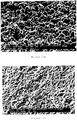
- a foil of copper as an electric conducting medium in a circuit for a circuit board in general is an electrolytic copper foil, that there is designed one surface thereof to be as a roughened surface and the opposite surface therefrom to be as a brightened surface by making use of an electroplating. Still further, there becomes to be produced such the electrolytic copper foil in usual, by generating the roughened surface thereof by making use of the electroplating, and then by further performing such as a plating of copper or the like thereon to be grown a protrusion as a fine bump shape thereon. Still further, there is shown in FIG. 16 a photo according to a scanning electron microscope regarding a roughened surface of such the electrolytic copper foil for a circuit board.
- the foil of copper with having a thickness as between 35 ⁇ m and 70 ⁇ m that it is able to produce the same by making use of the electroplating.
- it is not able to make use of a foil of copper with having the thickness as thicker than the above mentioned range of therebetween, due to becoming a period of time for plating to be so excessively longer that it excessively increases the cost for producing such the foil of copper.
- it is required for such the core in the metal core substrate for the circuit board to be as the roughened surfaces for the both surfaces thereof.
- a process for roughening a surface of a copper plate there is provided a process for roughening the surface of the copper plate by performing such as an etching therefor, a chemical treatment therefor, or the like. And then as a typical example thereof, it is able to be provided the CZ treatment that is proposed by MEC COMPANY LTD. Further, such the CZ treatment is a process to form a particle of copper to be etched and a coating film layer that is comprised of chemical compound of organic nitrogen on a surface of a copper plate, by making use of a reaction of oxidation or of reduction according to a chemical compound of bivalent copper.
- an object of the present invention is to provide a process for producing a copper plate to be roughened a surface thereof, and to provide an equipment for producing the same, by which a deterioration of an electroplating solution for plating copper thereon becomes hard to progress therein, and by which it becomes able to roughen the both surfaces of the copper plate at the same time therefor, that is independent of an existence or a nonexistence of any of holes thereon for individual through holes.
- a process for producing a copper plate to be roughened a surface thereof, for roughening the surface of the copper plate by forming a protrusion as a fine bump shape on the surface of the copper plate, according to the present invention is characterized in that it becomes able to form the protrusion as the fine bump shape thereon by comprising the following steps of: arranging electrodes as a similar pole for therebetween to be opposed to each other in an electroplating solution for plating copper; arranging the copper plate at between the electrodes; performing an anodic treatment for generating a fine particle of copper on both surfaces of the copper plate, by performing an electrolytic process with the copper plate as a positive electrode therefor and the electrodes as negative electrodes therefor; performing a cathodic treatment after performing the anodic treatment, by performing an electroplating of copper with the copper plate as a negative electrode therefor and the electrodes as positive electrodes therefor, for the fine particle of copper to be fixed onto the surfaces of the copper plate; and performing the anodic treatment and then the cathodic treatment,
- the process for producing the copper plate according to the present invention there may be designed to be performed a process for a plating of copper, for adjusting a thickness of the plate, with the copper plate as the negative electrode therefor and the electrodes as the positive electrodes therefor in an electroplating solution for plating copper in which there becomes to be performed the anodic treatment therefor and then the cathodic treatment therefor, before performing the anodic treatment for the first time.
- a process of roughening for the thickness of the plate after performing the process for the plating of copper for the adjustment of the thickness of the plate.
- the process for producing the copper plate according to the present invention may be able to produce a copper plate to be roughened a surface thereof as well, by comprising the following steps of: arranging one pair of electrodes as a similar pole for therebetween to be opposed to each other in an electroplating solution for plating copper; arranging a copper plate at between the one pair of the electrodes as the similar pole for therebetween; and performing the anodic treatment therefor and then the cathodic treatment therefor as not less than the one cycle thereof, without moving the copper plate at all for the electrodes as the similar pole for therebetween.
- the process for producing the copper plate according to the present invention may be able to produce a copper plate to be roughened a surface thereof as well, by comprising the following steps of: arranging one pair of positive electrodes to be opposed to each other in an electroplating solution for plating copper and one pair of negative electrodes to be opposed to each other in the similar solution to be in a tandem manner; arranging a copper plate at between the negative electrodes; performing an anodic treatment therefor with the copper plate as a positive electrode therefor; moving the copper plate relatively for between the positive electrodes; performing a cathodic treatment therefor with the copper plate as a negative electrode therefor; and performing the anodic treatment therefor and then the cathodic treatment therefor, that are defined to be as one cycle, as not less than the one cycle thereof.
- the process for producing the copper plate according to the present invention may be able to produce a copper plate to be roughened a surface thereof as well, by comprising the following steps of: arranging one pair or pairs as a plurality of positive electrodes (a group) to be opposed to each other in an electroplating solution for plating copper and one pair or pairs as a plurality of negative electrodes (a group) to be opposed to each other in the similar solution to be alternately in a tandem manner with having a number thereof as corresponding to a number of the cycles of the treatments therefor; moving a copper plate from between the electrodes at a side for one end thereof to between the electrodes at a side for the other end thereof as relatively one after the other; and performing the anodic treatment therefor and then the cathodic treatment therefor as one after the other.
- the process for producing the copper plate according to the present invention may be able to obtain the copper plates as the two sheets that become to be individually roughened one side of the surfaces for each thereof as well, by comprising the following steps of: performing an anodic treatment for a copper plate to be combined, that copper plates as two sheets are overlapped to be formed as a form of one sheet, by performing any one of the processes as defined above; performing a cathodic treatment therefor, by performing the processes in a similar manner; and separating the combined copper plate into each one of the copper plates.
- the anodic treatment therefor prefferably be performed with an electric current density of between 1 A/dm 2 and 8 A/dm 2 for between three minutes and ten minutes
- the cathodic treatment therefor to be performed with an electric current density of between 1 A/dm 2 and 8 A/dm 2 for between three minutes and ten minutes as well.
- the electroplating solution for plating copper it is desirable for the electroplating solution for plating copper to be maintained a temperature thereof as between 18 °C and 32 °C. Still further, it is further preferable for the electroplating solution for plating copper to be maintained the temperature thereof as between 24 °C and 30 °C.
- the process for producing the copper plate according to the present invention it is desirable to form beforehand a predetermined hole at a predetermined position on a copper plate, before performing any one of the anodic treatments therefor or of the cathodic treatments therefor.
- an equipment for producing a copper plate to be roughened a surface thereof it is desirable to be designed the same as comprising the following configuration of: an electrolytic bath for housing an electroplating solution for plating copper; one pair of positive electrodes to be opposed to each other in the electrolytic bath and to be arranged in a tandem manner therein; one pair of negative electrodes to be opposed to each other in the electrolytic bath and to be arranged in a tandem manner therein; a bus bar for a negative electrode, that is designed to be arranged horizontally at an upper side for between the one pair of the positive electrodes, and that is for hanging the copper plate; a bus bar for a positive electrode, that is designed to be arranged horizontally at an upper side for between the one pair of the negative electrodes, and that is for hanging the copper plate; and an insulating bar for connecting to between the bus bar for the negative electrode and the bus bar for the positive electrode.
- an equipment for producing a copper plate to be roughened a surface thereof it is further preferable to be designed the same as comprising the following configuration of: an electrolytic bath for housing an electroplating solution for plating copper; one pair or pairs as a plurality of positive electrodes (a group) to be opposed to each other in the electrolytic bath and one pair or pairs as a plurality of negative electrodes (a group) to be opposed to each other in the similar bath and to be arranged alternately in a tandem manner with having a number thereof as corresponding to a number of the cycles of the treatments therefor; a bus bar for a negative electrode, that is designed to be arranged horizontally at an upper side for between each of the individual pairs of the positive electrodes, and that is for hanging the copper plate; a bus bar for a positive electrode, that is designed to be arranged horizontally at an upper side for between each of the individual pairs of the negative electrodes, and that is for hanging the copper plate; and an insulating bar for connecting to between the bus bar for the
- a copper plate to be roughened a surface thereof is characterized in that a predetermined hole is designed to be formed at a predetermined position on the copper plate to be roughened a surface thereof, a grain size of a protrusion as a fine bump shape to be formed on the surface of the copper plate is designed to be as not larger than 10 ⁇ m, and a surface roughness thereof as an Rz is designed to be as between 3 ⁇ m and 20 ⁇ m.
- an inner face of the hole thereon it is desirable for an inner face of the hole thereon to be roughened, and then it is desirable as well for a height of a protrusion as a fine bump shape to be formed at the inner face of the hole thereon is designed to be as not higher than 20 ⁇ m.
- the present invention it becomes able to form the protrusion as the fine bump shape on both of the surfaces of the copper plate and then thereby to roughen both of such the surfaces of the copper plate, by comprising the following steps of: performing the anodic treatment for generating such the fine particle of copper on both of the surfaces of the copper plate, by performing the electrolytic process with the copper plate as the positive electrode therefor and the above mentioned electrodes as the negative electrodes therefor; performing the cathodic treatment therefor, by performing the plating of copper with the above mentioned copper plate as the negative electrode therefor and the above mentioned electrodes as the positive electrodes therefor, for the above mentioned fine particle of copper to be fixed onto the surfaces of the copper plate.
- the plates of copper as the two sheets that become to be individually roughened each one side of the surfaces for each thereof as well, by comprising the following steps of: performing the anodic treatment for the plate of copper to be combined, that the plates of copper as the two sheets are overlapped to be formed as the form of one sheet; performing the cathodic treatment therefor; and then thereafter separating such the combined plate of copper into each one of the plates of copper.
- FIG. 1 shows one embodiment according to the present invention.
- (1 ) designates an electrolytic bath
- (2) designates an electroplating solution for plating copper that is housed in the electrolytic bath (1)
- (3) and the other (3) designates electrodes as one pair that are arranged to be opposed to each other in the electroplating solution for plating copper (2)
- (4) designates a plate of copper that is arranged at between the electrodes as (3) and the other (3) to be roughened a surface thereof
- (5) designates a frame body for holding the plate of copper (4)
- (6) designates a hanger metal fitting therefor
- (7) designates a bus bar for maintaining the plate of copper (4) to be as a positive electrode or as a negative electrode via the hanger metal fitting (6) and the frame body (5).
- any electrical wiring to be shown in such the figure that is designed to maintain the electrodes as (3) and the other (3) to be an electric pole as opposite to that of the plate of copper (4).
- a plate of copper or a bar of copper for such the electrodes as (3) and the other (3) therein.
- an insoluble electrode to be on the market as well (such as an insoluble electrode of oxide based with making use of titanium to be as a base material therefor, an insoluble electrode of platinum based, or the like).
- the electrode normally to be made use of a member that has an area as opposed and then similar to one surface of the copper plate to be roughened thereby. However, it is all right to perform an increase or a decrease in such the area thereof, or to perform a division into a plurality of sheets therefor, as pursuant to the circumstances corresponding thereto.
- the electroplating solution for plating copper (2) is an electroplating solution for plating copper to be on the market .
- a composition of the solution for plating copper (2) to be as for example: sulfate of copper of between 40 g/l and 250 g/l; sulfuric acid of between 30 g/l and 210 g/l; hydrochloric acid of between 10 ppm and 80 ppm; and an additive agent, such as a brightening agent or the like, with a quantity to be specified by a maker therefor (as approximately between 2 ml/l and 10 ml/l).
- the solution for plating copper (2) to be agitated by making use of such as a unit for agitating pneumatically (a bubbling) that is arranged at a bottom part of the electrolytic bath (1), a jet nozzle to be arranged at between the electrode in the bath (1) and the plate of copper to be roughened the surface thereof, or the like (that are omitted to be shown in the figures).
- a unit for agitating pneumatically a bubbling
- a jet nozzle to be arranged at between the electrode in the bath (1) and the plate of copper to be roughened the surface thereof, or the like (that are omitted to be shown in the figures).
- such the fine particle of copper to be generated according to the process of the anodic treatment therefor is so called an anode slime as a nuisance in general at the period of the electroplating of copper, that is considered to be generated due to a retention of such as copper, copper oxide, ions of copper, or the like, with a concentration to be as higher on the surface of the copper plate, because of a difference between a rate of the copper ions to be precipitated from the plate of copper and a diffusion rate of the ions into the solution for plating thereof according to such the anodic treatment therefor.
- the fine particle of copper to be generated therein cannot help but be removed from the surface of the copper plate in a case where there is the quantity thereof as excessively larger, and then thereby it is not able to form the protrusion as the fine bump shape thereon. Still further, it is not able to form the protrusion as the fine bump shape thereon in a case where there is the quantity thereof as excessively smaller.
- a condition of the anodic treatment for the fine particle of copper to be generated therein with the quantity thereof to be required for forming the protrusion as the fine bump shape on the surface of the copper plate it is different from every case thereof due to such as a density of an electric current therethrough, an amount of time for processing thereof, a temperature of the solution therefor, or the like, and then it is evaluated experimentally.
- the condition of such the anodic treatment as preferred thereto according to the experiment therefor there are obtained that the density of the electric current therethrough as between 1 A/dm 2 and 8 A/dm 2 , the temperature of the solution therefor as between 18 °C and 32 °C, and that the amount of time for processing thereof as between three minutes and ten minutes.
- the cathodic treatment for such the fine particle of copper that becomes to be generated thereby, to be fixed onto the surfaces of the copper plate, it is evaluated experimentally as similar thereto. Still further, regarding the condition of such the cathodic treatment as preferred thereto according to the experiment therefor, there are obtained that the density of the electric current therethrough as between 1 A/dm 2 and 8 A/dm 2 , the temperature of the solution therefor as between 18 °C and 32 °C, and that the amount of time for processing thereof as between three minutes and ten minutes. Thus, such the individual conditions thereof are approximately similar to the individual conditions of the ordinary electroplating of copper respectively.
- an important point according to the present invention is that there becomes found out that it becomes able to form such the protrusion as the fine bump shape thereon, not by performing any processes of the electroplating of copper with the density of the electric current therethrough as higher, such as the process for roughening the surface of the electrolytic copper foil, but by performing the process for generating the fine particle of copper and then by performing the process for fixing the same thereon with making use of the individually conditions of the ordinary electroplating of copper.
- the copper plates as the two sheets that become to be individually roughened each one side of the surfaces for each thereof as well, by comprising the following steps of: performing the anodic treatment for the copper plate to be combined, that the copper plates as the two sheets are overlapped to be formed as the form of one sheet; performing the cathodic treatment therefor; and then thereafter separating such the combined copper plate into each one of the copper plates (it is similar for the embodiments as described below).
- FIG. 2 shows another embodiment according to the present invention. And then in FIG. 2 , there is made use of a similar symbol for a part therein as similar to that according to FIG. 1 .
- a point according to this embodiment to be different from that according to the first embodiment is that there are designed to be longer the electrolytic bath (1), to be arranged one pair of positive electrodes as (3a) and the other (3a) for becoming opposed to each other, and to be arranged one pair of negative electrodes as (3c) and the other (3c) for becoming opposed to each other, that are arranged in a tandem manner in the electroplating solution for plating copper (2) respectively.
- bus bar for a negative electrode (7c) that is designed to be arranged horizontally at an upper side for intermediately between the above mentioned one pair of the positive electrodes as (3a) and the other (3a) therein.
- bus bar for a positive electrode (7a) that is designed to be arranged horizontally at an upper side for intermediately between the above mentioned one pair of the negative electrodes as (3c) and the other (3c) therein.
- bus bar for the negative electrode (7c) and the bus bar for the positive electrode (7a) to be connected to therebetween in a linear form via an insulating bar (8).
- a copper plate to be roughened a surface thereof For producing a copper plate to be roughened a surface thereof by making use of such the equipment therefor, there is designed to be arranged the plate of copper (4) at between the negative electrodes therefor as (3c) and the other (3c) first of all with being hung up by making use of the bus bar for the positive electrode (7a) as shown in FIG. 2 (A) and in (B), and then to be performed an anodic treatment therefor with such the plate of copper (4) to be as the positive electrode therein. And then thereby there is designed to be generated a fine particle of copper with a quantity to be required for forming a protrusion as a fine bump shape on both of the surfaces of the copper plate (4).
- the hanger metal fitting (6) to be moved from the bus bar for the positive electrode (7a) over the insulating bar (8) and then to the bus bar for the negative electrode (7c), there is designed to be arranged the plate of copper (4) at between the positive electrodes as (3a) and the other (3a) thereafter, and then there is designed to be performed a cathodic treatment therefor with such the plate of copper (4) to be as the negative electrode therein under such the state thereof. And then by performing the process of such the cathodic treatment therefor (plating of copper thereon), there becomes to be fixed such the fine particle of copper onto the plate of copper, that is generated on the surfaces of the copper plate.
- FIG. 3 shows further another embodiment according to the present invention. And then in FIG. 3 , there is made use of a similar symbol for a part therein as similar to that according to FIG. 2 . Moreover, there is designed to be longer for a length of the electrolytic bath (1) as approximately two times as that of the equipment as shown in FIG.
- bus bar for the positive electrode (7a) that is designed to be arranged horizontally at the upper side for intermediately between the one pair of the negative electrodes as (3c) and the other (3c) therein. Furthermore, there are designed such the bus bar for the negative electrode (7c) and the bus bar for the positive electrode (7a), that are adjacent to each other, to be connected to therebetween in a linear form via the insulating bar (8).
- a copper plate to be roughened a surface thereof For producing a copper plate to be roughened a surface thereof by making use of such the equipment therefor, there may be designed to be moved the plate of copper (4) from between the negative electrodes as (3c) and the other (3c) at a side of one end in the electrolytic bath (1) (at left side in such the figure) to between the positive electrodes as (3a) and the other (3a) at a side of the other end therein as one after the other thereof, and then to be performed such the anodic treatment therefor and then the cathodic treatment therefor as one after the other thereof.
- a plate of copper or a bar of copper for such the negative electrodes as (3c) and the other (3c) therein. Still further, it may be able to make use of a plate of copper or a bar of copper for such the positive electrodes as (3a) and the other (3a) therein, however, it is desirable to make use of an insoluble electrode (such as an insoluble electrode of oxide based with making use of titanium to be as a base material therefor, an insoluble electrode of platinum based, or the like). Still further, there are designed for both of such the negative electrodes and such the positive electrodes normally to be individually made use of a member that has an area as opposed and then similar to one surface of the copper plate to be roughened thereby respectively. However, it is all right to perform an increase or a decrease in such the area thereof, or to perform a division into a plurality of sheets therefor, as pursuant to the circumstances corresponding thereto.
- it may be available to perform the individual processes of such the anodic treatment therefor and then such the cathodic treatment therefor as not less than three cycles thereof as required therefor. Furthermore, in the case of performing such the processes as not less than the three cycles thereof, it may be available to design to be arranged therein one pair of positive electrodes as (3a) and the other (3a) for becoming opposed to each other, and to be arranged therein one pair of negative electrodes as (3c) and the other (3c) for becoming opposed to each other, that are arranged alternately in a tandem manner as not less than three sets for each of such the pairs thereof respectively.
- the amount of time for such the anodic treatment therefor is longer than ten minutes, it is found out that there becomes a tendency that it becomes unable to form the protrusion as the fine bump shape thereon in a preferred way due to the quantity of the fine particles of copper to be formed on the surface of the copper plate as excessively larger.
- the density of the electric current therethrough is higher than 8 A/dm 2 , it is found out that there becomes a tendency that it becomes unable to form the protrusion as the fine bump shape thereon in a preferred way, because there becomes to be occurred a peeling off at such as an end face thereof or the like due to the quantity of the fine particles of copper to be formed on the surface of the copper plate as excessively larger.
- the density of the electric current therethrough is higher than 8 A/dm 2 , it is found out that there becomes a tendency that it becomes unable to form the protrusion as the fine bump shape thereon in a preferred way, because there becomes to be covered such the protrusion as the fine bump shape by a layer to be plated thereon due to the amount of the plating of copper thereon as excessively larger.
- the protrusion as the bump shape thereon means a form to be precipitated, such as attaching to each other with having a necking (constricted part) at between a base for the plate of copper and a particle or at between a particle and another particle. And then according to such the necking therebetween, there becomes to be functioned an effect of anchoring with between a resin of an insulating substrate. Hence, it becomes able to be improved thereby a strength of adhesive bonding for therebetween.
- such the form includes a case where there becomes to be a bump as a cluster shape (a bunch shape of grapes) by attaching the particles to each other, that a size thereof becomes to be as approximately between 1 ⁇ m and 20 ⁇ m.
- the grain size of such the protrusion as the bump shape thereon it is desirable therefor to be as not larger than 10 ⁇ m, because there becomes to be better the adherence of between such the protrusion and the base for the plate of copper in such the range thereof, and because there becomes to be better the strength of adhesive bonding with between the insulating substrate therein as well. Still further, in a case where the grain size of such the protrusion of the fine bump shape is between 0.5 ⁇ m and 3 ⁇ m, there becomes to be further preferable because there becomes to be enhanced a uniformity thereof and then thereby because there becomes to be further improved the strength of adhesive bonding for between such the protrusion and the base therefor.
- an Rz as a roughness that it is able to be measured as macroscopically. And then it is desirable for such the Rz thereon to be as between 3 ⁇ m and 20 ⁇ m, because there becomes to be better the adherence of between such the protrusion and the base therefor in such the range thereof, and because there becomes to be better the strength of adhesive bonding with between the insulating substrate therein as well. Still further, it becomes to be further preferable in a case where such the Rz thereon is between 7 ⁇ m and 16 ⁇ m, because there becomes to be enhanced a uniformity thereof and then thereby because there becomes to be further improved the strength of adhesive bonding for between such the particles and the base therefor.
- a height of such the bump in a case of a cluster shape thereof, it is considered that a height regarding a whole of such the cluster thereof is defined to be a height of the bump), it is desirable therefor to be as not higher than 20 ⁇ m. And then in such the range thereof, there is not happened at all for any of the holes to be smaller in the diameter thereof, there is not happened at all for any of the bumps thereon to be peeled off therefrom, or the like.
- a jig as arbitrary with corresponding to the requirement therefor, for performing a holding of the plate of copper to be performed roughening the surface thereof.
- a metal such as copper, an alloy of copper, a stainless metal, titanium, or the like.
- the plate of copper that is made use for each of the present examples is a rolled plate of tough pitch copper with having a dimension of 500 mm as a length thereof, 380 mm as a width thereof, and 400 ⁇ m or 200 ⁇ m as a thickness thereof.
- a composition of the electroplating solution therefor to be made use for the processes thereof is: sulfate of copper as 90 g/l; sulfuric acid as 180 g/l; and hydrochloric acid as 60 ppm. Still further, there is added a brightening agent and a restraining agent as the supplementary agents thereinto respectively, that are made use for a plating of bright copper in general, with a quantity to be specified by a maker therefor respectively.
- the grain size of the protrusion as the fine bump shape on the primary surface thereof is not larger than 3 ⁇ m, and that there becomes to be covered substantially all over the surface thereof uniformly with such the protrusion as the fine bump shape thereon. Still further, there becomes able to be recognized thereby that there is a part thereon to become the bump shape as the cluster shape, however, each of the grain size of such the part thereon and the height thereof is not more than 10 ⁇ m respectively.
- the surface roughness thereof is designed to be measured by making use of the microscope of color 3D for super deep shape measurement as the type of VK-9510, that is produced by KEYENCE CORPORATION. And then according thereto, the surface roughness thereof as the Rz becomes to be 7.5 ⁇ m.
- such the copper plate is designed for such the copper plate to be roughened the surface thereof to be attached a cellophane tape that is on the market and has a width of 10 mm approximately, and then thereafter there is designed the same to be performed a pulling off test therefor.
- a pulling off test therefor there is not found any peeling off of such the protrusion as the fine bump shape thereon at all, but there becomes to be peeled off only the adhesive agent of the cellophane tape from the interface of such the cellophane tape, and then there becomes to be remained such the adhesive agent of the cellophane tape on such the copper plate to be roughened the surface thereof.
- the surface roughness thereof is designed to be measured by making use of the microscope of color 3D for super deep shape measurement as the type of VK-9510, that is produced by KEYENCE CORPORATION. And then according thereto, the surface roughness thereof as the Rz becomes to be 11.0 ⁇ m.
- such the copper plate is designed for such the copper plate to be roughened the surface thereof to be attached a cellophane tape that is on the market and has the width of 10 mm approximately, and then thereafter there is designed the same to be performed a pulling off test therefor.
- a pulling off test therefor there is not found any peeling off of such the protrusion as the fine bump shape thereon at all, but there becomes to be peeled off only the adhesive agent of the cellophane tape from the interface of such the cellophane tape, and then there becomes to be remained such the adhesive agent of the cellophane tape on such the copper plate to be roughened the surface thereof.
- the surface roughness thereof is designed to be measured by making use of the microscope of color 3D for super deep shape measurement as the type of VK-9510, that is produced by KEYENCE CORPORATION. And then according thereto, the surface roughness thereof as the Rz becomes to be 15.0 ⁇ m.
- such the copper plate is designed for such the copper plate to be roughened the surface thereof to be attached a cellophane tape that is on the market and has the width of 10 mm approximately, and then thereafter there is designed the same to be performed a pulling off test therefor.
- a pulling off test therefor there is not found any peeling off of such the protrusion as the fine bump shape thereon at all, but there becomes to be peeled off only the adhesive agent of the cellophane tape from the interface of such the cellophane tape, and then there becomes to be remained such the adhesive agent of the cellophane tape on such the copper plate to be roughened the surface thereof.
- the strength against peeling therefrom after performing the process for the solder to be heat resistant there becomes to be obtained the minimum value for all over such the plate as 1.9 kN/m, the maximum value therefor as 2.8 kN/m, and the mean value therefor as 2.4 kN/m. Furthermore, there becomes to be obtained such the strength against peeling therefrom, with sufficiently satisfying the strength of adhesive bonding for between the metal core and the insulating substrate, that is required for the metal core substrate for the circuit board (as not weaker than 1 kN/m).
- the surface roughness thereof is designed to be measured by making use of the microscope of color 3D for super deep shape measurement as the type of VK-9510, that is produced by KEYENCE CORPORATION. And then according thereto, the surface roughness thereof as the Rz becomes to be 4.0 ⁇ m.
- holes as a plurality thereof individually for the through holes on a plate of copper for a core that has a thickness of between 200 ⁇ m and 400 ⁇ m by making use of a drill, with having individual diameters of between 3 mm and 5 mm respectively.
- it may be available to be formed such the holes by punching out with making use of a press machine, because there may become to be required such the holes as a significant number thereof that may depend on a specification of a design for a substrate.
- each of (A) shows the primary surface thereof with a multiplying factor of 3000 times therefor according to the SEM respectively
- each of (B) shows an inner face of a hole thereon with a multiplying factor of 3000 times therefor according to the SEM respectively
- each of (C) shows an edge part of a hole thereon with a multiplying factor of 125 times therefor according to the SEM respectively.
- Example 5 it becomes clear that the grain size of the protrusion as the fine bump shape on the primary surface thereof is not larger than 3 ⁇ m, and that there is a part thereon to become the bump shape as the cluster shape, and then that each of the grain size of such the part thereon and the height thereof is not more than 10 ⁇ m respectively. Still further, it becomes clear that the surface roughness thereof as the Rz becomes to be 8.0 ⁇ m. Still further, there becomes to be roughened the inner face of such the hole thereon as well, and then it becomes clear that the height of such the protrusion as the bump shape at such the inner face thereof is not higher than 15 ⁇ m respectively.
- Example 6 it becomes clear that the grain size of the protrusion as the fine bump shape on the primary surface thereof is not larger than 3 ⁇ m, and that there is a part thereon to become the bump shape as the cluster shape, and then that each of the grain size of such the part thereon and the height thereof is not more than 10 ⁇ m respectively. Still further, it becomes clear that the surface roughness thereof as the Rz becomes to be 7.0 ⁇ m. Still further, there becomes to be roughened the inner face of such the hole thereon as well, and then it becomes clear that the height of such the protrusion as the bump shape at such the inner face thereof is not higher than 10 ⁇ m respectively.
- Example 7 it becomes clear that the grain size of the protrusion as the fine bump shape on the primary surface thereof is not larger than 3 ⁇ m, and that there is a part thereon to become the bump shape as the cluster shape, and then that each of the grain size of such the part thereon and the height thereof is not more than 10 ⁇ m respectively. Still further, it becomes clear that the surface roughness thereof as the Rz becomes to be 11.0 ⁇ m. Still further, there becomes to be roughened the inner face of such the hole thereon as well, and then it becomes clear that the height of such the protrusion as the bump shape at such the inner face thereof is not higher than 5 ⁇ m respectively.
- the surface roughness as the Rz on the primary surface thereof becomes to be 2.5 ⁇ m.
- the surface roughness as the Rz on the primary surface thereof becomes to be 2.0 ⁇ m.
- such the copper plate there is designed for such the copper plate to be roughened the surface thereof to be attached a cellophane tape that is on the market and has the width of 10 mm approximately, and then thereafter there is designed the same to be performed a pulling off test therefor. As a result thereof, there becomes to be peeled off such the part of the black color therefrom. And then thereby it becomes unable to be made use of such the plate for a metal core.
- the plate of copper there becomes to be as not smaller than 20 ⁇ m for a size of the protrusion as the bump shape at the inner face thereof, that is a difference between a concave thereon and a convex thereon, comparing to that according to the primary surface thereof. Still further, even in the case of performing an adjustment of the condition for such the electroplating thereof, it becomes unable to form any of the protrusion as the bump shape as uniformly thereon with including such the two of the faces thereof.
- a cause of such the matter is that there is designed to be made use of the density of the electric current as a larger amount therethrough according to such the process of the conventional electroplating thereof, and then thereby that there becomes to be convergent such the electric current as the larger amount from the electrode to each of the inner faces of the individual holes thereon, that have the surfaces with an area in total as smaller, at the places that each of such the holes passes therethrough comparing to other places on the surfaces of such the plate of copper that is designed to be faced to the electrode therefor.
- the plate of copper for the metal core that has any of the holes individually for the through holes in particular, it becomes able to form the protrusion as the fine bump shape on the surface of the copper plate, by making use of such the processes according to the present invention, after forming any of the holes on such the plate of copper, and then thereby that it becomes able to perform the process of roughening as uniformly for the surface thereof and for the inner face of any of the holes thereon, therefore that it is the optimum therefor.
Landscapes
- Chemical & Material Sciences (AREA)
- Engineering & Computer Science (AREA)
- Organic Chemistry (AREA)
- Electrochemistry (AREA)
- Materials Engineering (AREA)
- Metallurgy (AREA)
- Chemical Kinetics & Catalysis (AREA)
- Crystallography & Structural Chemistry (AREA)
- Manufacturing & Machinery (AREA)
- Microelectronics & Electronic Packaging (AREA)
- Electroplating Methods And Accessories (AREA)
- Electroplating And Plating Baths Therefor (AREA)
- Parts Printed On Printed Circuit Boards (AREA)
Claims (10)
- Verfahren zur Herstellung einer Kupferplatte (4) mit einer aufgerauten Oberfläche, bei dem Vorsprünge mit einer feinen Buckelform auf einer Oberfläche einer Kupferplatte gebildet werden, um die Oberfläche der Kupferplatte aufzurauen, wobei die Vorsprünge mit einer feinen Buckelform gebildet werden durch:Anordnen eines Elektrodenpaares (3, 3a, 3c) gleicher Polarität gegenüber voneinander in einer Galvanisierungslösung zur Kupferbeschichtung;Anordnen der Kupferplatte zwischen den Elektroden;Durchführen mindestens eines Zyklus einer anodischen Behandlung und einer kathodischen Behandlung, wobei ein Zyklus aus einer anodischen Behandlung, bei der feine Kupferpartikel auf beiden Oberflächen der Kupferplatte erzeugt werden, indem ein elektrolytisches Verfahren mit der Kupferplatte als eine positive Elektrode und den Elektroden als negative Elektroden durchgeführt wird, und aus einer nach der anodischen Behandlung durchgeführten kathodischen Behandlung besteht, bei der die feinen Kupferpartikel auf den Oberflächen der Kupferplatte befestigt werden, indem eine Kupfergalvanisierung mit der Kupferplatte als einer negativen Elektrode und den Elektroden als positive Elektroden durchgeführt wird, ohne die Kupferplatte in Bezug auf die Elektroden zu bewegen.
- Verfahren zur Herstellung einer Kupferplatte (4) mit einer aufgerauten Oberfläche, bei dem Vorsprünge mit einer feinen Buckelform auf einer Oberfläche einer Kupferplatte gebildet werden, um die Oberfläche der Kupferplatte aufzurauen, wobei die Vorsprünge mit einer feinen Buckelform gebildet werden durch:Anordnen von mindestens zwei Elektrodenpaaren (3, 3a, 3c), welche ein Paar positive Elektroden und ein Paar negative Elektroden enthalten, in derselben Galvanisierungslösung zur Kupferbeschichtung, wobei die Elektroden jedes Paares die gleiche Polarität aufweisen und gegenüber voneinander angeordnet sind;Anordnen der Kupferplatte zwischen den Elektroden eines der Elektrodenpaare;Durchführen mindestens eines Zyklus einer anodischen Behandlung und einer kathodischen Behandlung, wobei der Zyklus aus dem Durchführen einer anodischen Behandlung, wobei die Kupferplatte stationär zwischen den Elektroden des negativen Elektrodenpaares angeordnet ist, und wobei die Kupferplatte als eine positive Elektrode dient, aus dem anschließenden Bewegen der Kupferplatte zu einer stationären Position zwischen den Elektroden des positiven Elektrodenpaares und aus dem Durchführen einer kathodischen Behandlung mit der Kupferplatte als eine negative Elektrode besteht.
- Verfahren zur Herstellung einer Kupferplatte mit einer aufgerauten Oberfläche nach Anspruch 2, umfassend:abwechselndes Anordnen eines Paares oder einer Vielzahl von Paaren positiver Elektroden gegenüber voneinander und eines Paares oder einer Vielzahl von Paaren negativer Elektroden gegenüber voneinander in einer Galvanisierungslösung zur Kupferbeschichtung, wobei sich die Elektrodenpaare auf zwei parallelen Linien erstrecken;sukzessives Bewegen der Kupferplatte von einer Position zwischen den Elektroden an einem Ende zu einer Position zwischen den Elektroden am anderen Ende und abwechselndes Durchführen der anodischen Behandlung und der kathodischen Behandlung.
- Verfahren zur Herstellung einer Kupferplatte mit einer aufgerauten Oberfläche, umfassend:Durchführen des in einem der Ansprüche 1 bis 3 definierten Verfahrens an einer kombinierten Kupferplatte, bei der zwei Kupferplatten übereinandergelegt werden, um ein Blatt zu bilden; undErhalten von zwei Kupferplatten, die jeweils auf einer Seite eine aufgeraute Oberfläche aufweisen, durch Trennen der kombinierten Kupferplatte in einzelne Kupferplatten.
- Verfahren zur Herstellung einer Kupferplatte mit einer aufgerauten Oberfläche nach einem der Ansprüche 1 bis 4, wobei die anodische Behandlung mit einer elektrischen Stromdichte zwischen 1 A/dm2 und 8 A/dm2 zwischen drei und zehn Minuten lang durchgeführt wird und die kathodische Behandlung mit einer elektrischen Stromdichte zwischen 1 A/dm2 und 8 A/dm2 zwischen drei und zehn Minuten lang durchgeführt wird.
- Verfahren zur Herstellung einer Kupferplatte mit einer aufgerauten Oberfläche nach Anspruch 5, wobei die Galvanisierungslösung zur Kupferbeschichtung bei einer Temperatur von 18°C bis 32°C gehalten wird.
- Verfahren zur Herstellung einer Kupferplatte mit einer aufgerauten Oberfläche nach einem der Ansprüche 1 bis 6, umfassend:
Bilden, im Voraus, eines vorbestimmten Lochs an einer vorbestimmten Position auf einer Kupferplatte, bevor die anodische Behandlung oder die kathodische Behandlung durchgeführt wird. - Verfahren zur Herstellung einer Kupferplatte mit einer aufgerauten Oberfläche nach einem der Ansprüche 1 bis 7, wobei ein Kupferbeschichtungsverfahren mit der Kupferplatte als die negative Elektrode und den Elektroden als die positiven Elektroden in einer Galvanisierungslösung zur Kupferbeschichtung durchgeführt wird, bevor die anodische Behandlung zum ersten Mal durchgeführt wird.
- Vorrichtung zum Herstellen einer Kupferplatte (4) mit einer aufgerauten Oberfläche, umfassend:ein elektrolytisches Bad (1) zur Aufnahme einer Galvanisierungslösung zur Kupferbeschichtung;ein Paar oder eine Vielzahl von Paaren von positiven Elektroden (3a), die im elektrolytischen Bad gegenüber voneinander angeordnet sind, wobei sich die positiven Elektrodenpaare auf zwei parallelen Linien erstrecken;ein Paar oder eine Vielzahl von Paaren von negativen Elektroden (3c), die im elektrolytischen Bad gegenüber voneinander angeordnet sind, wobei sich die negativen Elektrodenpaare auf zwei parallelen Linien erstrecken;eine negative Elektrodensammelschiene (7c), die horizontal über einer Stelle zwischen dem Paar oder den Paaren von positiven Elektroden angeordnet ist und die zum Aufhängen der Kupferplatte dient;eine positive Elektrodensammelschiene (7a), die horizontal über einer Stelle zwischen dem Paar oder den Paaren von negativen Elektroden angeordnet ist und die zum Aufhängen der Kupferplatte dient;eine Isolierschiene (8), die die negative Elektrodenschiene und die positive Elektrodenschiene koppelt;einen Rahmenkörper (5) zum Halten der Kupferplatte (4); undeine Metallbeschlagaufhängung (6) für den Rahmenkörper (5).
- Vorrichtung nach Anspruch 9,
wobei die positiven und negativen Elektrodenpaare abwechselnd angeordnet sind, und
wobei die Isolierschiene benachbarte negative und positive Elektrodensammelschienen koppelt.
Applications Claiming Priority (2)
| Application Number | Priority Date | Filing Date | Title |
|---|---|---|---|
| JP2007052568 | 2007-03-02 | ||
| PCT/JP2008/053786 WO2008108341A1 (ja) | 2007-03-02 | 2008-03-03 | 表面粗化銅板の製造方法及び装置、並びに表面粗化銅板 |
Publications (3)
| Publication Number | Publication Date |
|---|---|
| EP2133448A1 EP2133448A1 (de) | 2009-12-16 |
| EP2133448A4 EP2133448A4 (de) | 2011-04-27 |
| EP2133448B1 true EP2133448B1 (de) | 2019-10-30 |
Family
ID=39738219
Family Applications (1)
| Application Number | Title | Priority Date | Filing Date |
|---|---|---|---|
| EP08721206.4A Active EP2133448B1 (de) | 2007-03-02 | 2008-03-03 | Verfahren und vorrichtung zur herstellung einer oberflächenaufgerauhten kupferplatte |
Country Status (5)
| Country | Link |
|---|---|
| US (2) | US8815072B2 (de) |
| EP (1) | EP2133448B1 (de) |
| JP (2) | JP5323677B2 (de) |
| CN (2) | CN101622380B (de) |
| WO (1) | WO2008108341A1 (de) |
Families Citing this family (18)
| Publication number | Priority date | Publication date | Assignee | Title |
|---|---|---|---|---|
| JP2832894B2 (ja) | 1988-07-26 | 1998-12-09 | 日立建機株式会社 | 圧力センサ及びその製造方法、並びに圧力センサを備える油圧機器 |
| JP5448710B2 (ja) * | 2009-10-19 | 2014-03-19 | 古河電気工業株式会社 | 表面粗化銅板の製造方法および製造装置 |
| US9058973B2 (en) * | 2011-04-13 | 2015-06-16 | International Business Machines Corporation | Passive devices fabricated on glass substrates, methods of manufacture and design structures |
| JP5839876B2 (ja) * | 2011-07-27 | 2016-01-06 | 古河電気工業株式会社 | レーザ加工用銅板および該レーザ加工用銅板を用いたプリント基板、並びに銅板のレーザ加工方法 |
| EP2818579A4 (de) * | 2012-02-24 | 2015-11-11 | Jfe Steel Corp | Metallmaterial und oberflächenbehandlungsverfahren sowie vorrichtung |
| JP6062341B2 (ja) * | 2013-10-23 | 2017-01-18 | 古河電気工業株式会社 | 銅・樹脂複合体、及びその製造方法 |
| DE102014211298A1 (de) * | 2014-06-13 | 2015-12-17 | Robert Bosch Gmbh | Substrat mit einer Oberflächenbeschichtung und Verfahren zum Beschichten einer Oberfläche eines Substrates |
| JP6867102B2 (ja) * | 2014-10-22 | 2021-04-28 | Jx金属株式会社 | 銅放熱材、キャリア付銅箔、コネクタ、端子、積層体、シールド材、プリント配線板、金属加工部材、電子機器、及び、プリント配線板の製造方法 |
| KR101615552B1 (ko) * | 2014-11-17 | 2016-04-27 | 에스피텍 주식회사 | 다공성 구조를 가지는 도금층의 제조방법 |
| JP6188959B2 (ja) | 2015-02-26 | 2017-08-30 | コーニンクレッカ フィリップス エヌ ヴェKoninklijke Philips N.V. | アタッチメントコーム及びヘアカッティング器具 |
| CN106637318A (zh) * | 2015-10-29 | 2017-05-10 | 神华集团有限责任公司 | 一种纳米结构阵列及其制备方法 |
| CN108432352B (zh) * | 2015-12-25 | 2019-11-26 | 太阳诱电株式会社 | 印刷布线板和摄像组件 |
| JP7068341B2 (ja) * | 2017-12-26 | 2022-05-16 | Jx金属株式会社 | 放熱用銅箔及び放熱部材 |
| CN108330489A (zh) * | 2018-04-20 | 2018-07-27 | 云南惠铜新材料科技有限公司 | 一种平滑轮廓铜箔表面粗化处理方法 |
| CN114521069B (zh) * | 2020-11-19 | 2024-02-23 | 健鼎(无锡)电子有限公司 | 铜块棕化治具及其制造方法 |
| KR102454686B1 (ko) * | 2020-12-30 | 2022-10-13 | 에스케이씨 주식회사 | 표면 처리 동박 및 이를 포함하는 회로 기판 |
| CN114108055A (zh) * | 2021-12-30 | 2022-03-01 | 四会富仕电子科技股份有限公司 | 一种电解粗化铜面的方法 |
| CN117956692B (zh) * | 2024-03-27 | 2024-05-28 | 深圳市板明科技股份有限公司 | 一种线路板碱性去悬铜液及其制备方法与去悬铜方法 |
Citations (1)
| Publication number | Priority date | Publication date | Assignee | Title |
|---|---|---|---|---|
| EP0709494A2 (de) * | 1994-10-06 | 1996-05-01 | Circuit Foil Japan Co., Ltd. | Verfahren zur Oberflächen-Aufrauhung von Kupferfolie |
Family Cites Families (25)
| Publication number | Priority date | Publication date | Assignee | Title |
|---|---|---|---|---|
| GB1199089A (en) * | 1967-11-22 | 1970-07-15 | Nippon Kokan Kk | A Method of Electrolytically Treating Metal Articles |
| JPS5937760B2 (ja) * | 1978-10-25 | 1984-09-11 | 株式会社フジクラ | 交流電解メツキによる表面処理方法 |
| JPS58151465A (ja) * | 1982-03-03 | 1983-09-08 | Sanwa Bousei Kk | 片面めつき方法 |
| JPS58164797A (ja) * | 1982-03-05 | 1983-09-29 | オリン・コ−ポレ−シヨン | 結合強さを改良する銅の電気化学的処理 |
| US4443304A (en) * | 1982-10-01 | 1984-04-17 | Micro-Plate, Inc. | Plating system and method |
| FR2542766B1 (fr) * | 1983-03-16 | 1987-07-03 | Cegedur | Procede et dispositif de traitement electrochimique de la surface de produits metalliques de forme allongee |
| US4552627A (en) * | 1984-11-13 | 1985-11-12 | Olin Corporation | Preparation for improving the adhesion properties of metal foils |
| JPS6333600A (ja) | 1986-07-29 | 1988-02-13 | Nippon Steel Corp | 鋼ストリツプの電解酸洗法 |
| JPS63273790A (ja) * | 1987-05-06 | 1988-11-10 | Mitsubishi Metal Corp | 伝熱体およびその製造方法 |
| JP2662011B2 (ja) * | 1989-02-02 | 1997-10-08 | 古河電気工業株式会社 | 早期に緑青が形成する屋根板材 |
| JP2660583B2 (ja) * | 1989-08-24 | 1997-10-08 | 富士写真フイルム株式会社 | 印刷版用アルミニウム支持体の電解処理方法 |
| JPH0382880A (ja) | 1989-08-25 | 1991-04-08 | Shigenori Sakuma | 絞染め方法 |
| JPH03202500A (ja) * | 1989-08-28 | 1991-09-04 | Matsushita Electric Works Ltd | 銅箔の粗面化方法 |
| CN1174252A (zh) * | 1996-08-16 | 1998-02-25 | 柯建信 | 滚轮输送式印刷电路板铜表面反电解清洁粗化法 |
| US5863410A (en) * | 1997-06-23 | 1999-01-26 | Circuit Foil Usa, Inc. | Process for the manufacture of high quality very low profile copper foil and copper foil produced thereby |
| JPH11298103A (ja) * | 1998-04-10 | 1999-10-29 | Mitsubishi Plastics Ind Ltd | 銅コア銅張積層板および銅コアプリント基板 |
| JP2001011694A (ja) * | 1999-06-25 | 2001-01-16 | Fuji Photo Film Co Ltd | 電解処理方法 |
| JP2001210932A (ja) * | 2000-01-26 | 2001-08-03 | Matsushita Electric Works Ltd | プリント配線板の製造方法 |
| JP2002332544A (ja) * | 2001-05-08 | 2002-11-22 | Hitachi Metals Ltd | メタルコア基板用金属板およびその製造方法およびそれを用いたメタルコア基板、ビルドアップ基板 |
| US6969557B2 (en) * | 2002-06-04 | 2005-11-29 | Mitsui Mining & Smelting Co., Ltd. | Surface-treated copper foil low-dielectric substrate and copper-clad laminate and printed wiring board using the same |
| CN1534112A (zh) * | 2003-04-02 | 2004-10-06 | 联华电子股份有限公司 | 一种避免电镀沉积铜薄膜生成空穴的装置及其使用方法 |
| JP2005008973A (ja) | 2003-06-20 | 2005-01-13 | Hitachi Cable Ltd | 銅箔の表面粗化方法 |
| JP2005072184A (ja) * | 2003-08-22 | 2005-03-17 | Osamu Nagai | メタルコアと多層基板の複合基板 |
| EP1678352A2 (de) * | 2003-10-22 | 2006-07-12 | Nexx Systems, Inc. | Verfahren und vorrichtung zur fluidverarbeitung eines werkstücks |
| JP4609850B2 (ja) * | 2005-08-01 | 2011-01-12 | 古河電気工業株式会社 | 積層回路基板 |
-
2008
- 2008-03-03 EP EP08721206.4A patent/EP2133448B1/de active Active
- 2008-03-03 CN CN2008800069014A patent/CN101622380B/zh active Active
- 2008-03-03 CN CN201110441836.1A patent/CN102517617B/zh active Active
- 2008-03-03 JP JP2009502576A patent/JP5323677B2/ja active Active
- 2008-03-03 WO PCT/JP2008/053786 patent/WO2008108341A1/ja not_active Ceased
- 2008-03-03 US US12/529,560 patent/US8815072B2/en active Active
-
2013
- 2013-06-06 JP JP2013120000A patent/JP5684328B2/ja active Active
-
2014
- 2014-07-22 US US14/337,264 patent/US9758890B2/en active Active
Patent Citations (1)
| Publication number | Priority date | Publication date | Assignee | Title |
|---|---|---|---|---|
| EP0709494A2 (de) * | 1994-10-06 | 1996-05-01 | Circuit Foil Japan Co., Ltd. | Verfahren zur Oberflächen-Aufrauhung von Kupferfolie |
Also Published As
| Publication number | Publication date |
|---|---|
| EP2133448A1 (de) | 2009-12-16 |
| CN102517617B (zh) | 2014-12-31 |
| EP2133448A4 (de) | 2011-04-27 |
| CN102517617A (zh) | 2012-06-27 |
| JPWO2008108341A1 (ja) | 2010-06-17 |
| CN101622380B (zh) | 2012-05-30 |
| US8815072B2 (en) | 2014-08-26 |
| JP2013177695A (ja) | 2013-09-09 |
| US9758890B2 (en) | 2017-09-12 |
| JP5323677B2 (ja) | 2013-10-23 |
| US20100304176A1 (en) | 2010-12-02 |
| US20140339094A1 (en) | 2014-11-20 |
| WO2008108341A1 (ja) | 2008-09-12 |
| JP5684328B2 (ja) | 2015-03-11 |
| CN101622380A (zh) | 2010-01-06 |
Similar Documents
| Publication | Publication Date | Title |
|---|---|---|
| EP2133448B1 (de) | Verfahren und vorrichtung zur herstellung einer oberflächenaufgerauhten kupferplatte | |
| KR100407732B1 (ko) | 결절상구리/니켈합금피막을포함하는복합호일,이를포함하는인쇄회로기판및결절상구리/니켈합금피막의전착방법 | |
| KR100371524B1 (ko) | 동박의표면조화처리방법 | |
| EP0405369B1 (de) | Verfahren zur Herstellung eines kupferkaschierten Laminats | |
| US6777108B1 (en) | Electrolytic copper foil with carrier foil and method for manufacturing the same and copper-clad laminate using the electrolytic copper foil with carrier foil | |
| US6827833B2 (en) | Electrodeposition of metals in high-aspect ratio cavities using modulated reverse electric fields | |
| CN101695215A (zh) | 具有低断面的结合增强的铜箔 | |
| WO2010093009A1 (ja) | 金属箔およびその製造方法,絶縁基板,配線基板 | |
| US4961828A (en) | Treatment of metal foil | |
| US4551210A (en) | Dendritic treatment of metallic surfaces for improving adhesive bonding | |
| US20040108211A1 (en) | Surface treatment for a wrought copper foil for use on a flexible printed circuit board (FPCB) | |
| JP4429539B2 (ja) | ファインパターン用電解銅箔 | |
| EP0495468B1 (de) | Verfahren zur Herstellung behandelter Kupfer-Folien, daraus hergestellte Produkte sowie Elektrolyt zur Verwendung in einem solchen Verfahren | |
| EP0250195A2 (de) | Kupferfolie mit einer matten Oberfläche auf beiden Seiten | |
| WO2001034880A1 (en) | Electrolytic copper foil with carrier foil and method for manufacturing the same | |
| JPH09272994A (ja) | ファインパターン用電解銅箔 | |
| CN100572608C (zh) | 铜箔的粗面化处理方法以及粗面化处理液 | |
| JP3361914B2 (ja) | 印刷回路用銅箔の製造方法 | |
| US4552627A (en) | Preparation for improving the adhesion properties of metal foils | |
| JPH0328389A (ja) | 銅張積層板用銅箔層、その製造方法およびそれに用いるめっき浴 | |
| CN110528042A (zh) | 一种半导体器件电镀方法及用于电镀的活化槽 | |
| JP2927968B2 (ja) | 高密度多層プリント回路内層用銅箔および該銅箔を内層回路用に用いた高密度多層プリント回路基板 | |
| JPH0397876A (ja) | 銅箔の表面処理方法 | |
| JP2002105699A (ja) | 銅張り積層板用電解銅箔及びその製造方法 | |
| JP2004099950A (ja) | 銅箔の連続電解厚めっき方法及び装置 |
Legal Events
| Date | Code | Title | Description |
|---|---|---|---|
| PUAI | Public reference made under article 153(3) epc to a published international application that has entered the european phase |
Free format text: ORIGINAL CODE: 0009012 |
|
| 17P | Request for examination filed |
Effective date: 20090930 |
|
| AK | Designated contracting states |
Kind code of ref document: A1 Designated state(s): AT BE BG CH CY CZ DE DK EE ES FI FR GB GR HR HU IE IS IT LI LT LU LV MC MT NL NO PL PT RO SE SI SK TR |
|
| RAP1 | Party data changed (applicant data changed or rights of an application transferred) |
Owner name: FURUKAWA ELECTRIC CO., LTD. |
|
| DAX | Request for extension of the european patent (deleted) | ||
| A4 | Supplementary search report drawn up and despatched |
Effective date: 20110330 |
|
| 17Q | First examination report despatched |
Effective date: 20150318 |
|
| STAA | Information on the status of an ep patent application or granted ep patent |
Free format text: STATUS: EXAMINATION IS IN PROGRESS |
|
| GRAP | Despatch of communication of intention to grant a patent |
Free format text: ORIGINAL CODE: EPIDOSNIGR1 |
|
| STAA | Information on the status of an ep patent application or granted ep patent |
Free format text: STATUS: GRANT OF PATENT IS INTENDED |
|
| INTG | Intention to grant announced |
Effective date: 20190318 |
|
| GRAJ | Information related to disapproval of communication of intention to grant by the applicant or resumption of examination proceedings by the epo deleted |
Free format text: ORIGINAL CODE: EPIDOSDIGR1 |
|
| STAA | Information on the status of an ep patent application or granted ep patent |
Free format text: STATUS: EXAMINATION IS IN PROGRESS |
|
| INTC | Intention to grant announced (deleted) | ||
| GRAJ | Information related to disapproval of communication of intention to grant by the applicant or resumption of examination proceedings by the epo deleted |
Free format text: ORIGINAL CODE: EPIDOSDIGR1 |
|
| GRAR | Information related to intention to grant a patent recorded |
Free format text: ORIGINAL CODE: EPIDOSNIGR71 |
|
| GRAS | Grant fee paid |
Free format text: ORIGINAL CODE: EPIDOSNIGR3 |
|
| STAA | Information on the status of an ep patent application or granted ep patent |
Free format text: STATUS: GRANT OF PATENT IS INTENDED |
|
| GRAA | (expected) grant |
Free format text: ORIGINAL CODE: 0009210 |
|
| STAA | Information on the status of an ep patent application or granted ep patent |
Free format text: STATUS: THE PATENT HAS BEEN GRANTED |
|
| INTC | Intention to grant announced (deleted) | ||
| INTG | Intention to grant announced |
Effective date: 20190919 |
|
| AK | Designated contracting states |
Kind code of ref document: B1 Designated state(s): AT BE BG CH CY CZ DE DK EE ES FI FR GB GR HR HU IE IS IT LI LT LU LV MC MT NL NO PL PT RO SE SI SK TR |
|
| REG | Reference to a national code |
Ref country code: GB Ref legal event code: FG4D |
|
| REG | Reference to a national code |
Ref country code: CH Ref legal event code: EP |
|
| REG | Reference to a national code |
Ref country code: AT Ref legal event code: REF Ref document number: 1196231 Country of ref document: AT Kind code of ref document: T Effective date: 20191115 |
|
| REG | Reference to a national code |
Ref country code: DE Ref legal event code: R096 Ref document number: 602008061525 Country of ref document: DE |
|
| REG | Reference to a national code |
Ref country code: IE Ref legal event code: FG4D |
|
| REG | Reference to a national code |
Ref country code: LT Ref legal event code: MG4D |
|
| PG25 | Lapsed in a contracting state [announced via postgrant information from national office to epo] |
Ref country code: PT Free format text: LAPSE BECAUSE OF FAILURE TO SUBMIT A TRANSLATION OF THE DESCRIPTION OR TO PAY THE FEE WITHIN THE PRESCRIBED TIME-LIMIT Effective date: 20200302 Ref country code: NO Free format text: LAPSE BECAUSE OF FAILURE TO SUBMIT A TRANSLATION OF THE DESCRIPTION OR TO PAY THE FEE WITHIN THE PRESCRIBED TIME-LIMIT Effective date: 20200130 Ref country code: FI Free format text: LAPSE BECAUSE OF FAILURE TO SUBMIT A TRANSLATION OF THE DESCRIPTION OR TO PAY THE FEE WITHIN THE PRESCRIBED TIME-LIMIT Effective date: 20191030 Ref country code: BG Free format text: LAPSE BECAUSE OF FAILURE TO SUBMIT A TRANSLATION OF THE DESCRIPTION OR TO PAY THE FEE WITHIN THE PRESCRIBED TIME-LIMIT Effective date: 20200130 Ref country code: LV Free format text: LAPSE BECAUSE OF FAILURE TO SUBMIT A TRANSLATION OF THE DESCRIPTION OR TO PAY THE FEE WITHIN THE PRESCRIBED TIME-LIMIT Effective date: 20191030 Ref country code: SE Free format text: LAPSE BECAUSE OF FAILURE TO SUBMIT A TRANSLATION OF THE DESCRIPTION OR TO PAY THE FEE WITHIN THE PRESCRIBED TIME-LIMIT Effective date: 20191030 Ref country code: PL Free format text: LAPSE BECAUSE OF FAILURE TO SUBMIT A TRANSLATION OF THE DESCRIPTION OR TO PAY THE FEE WITHIN THE PRESCRIBED TIME-LIMIT Effective date: 20191030 Ref country code: GR Free format text: LAPSE BECAUSE OF FAILURE TO SUBMIT A TRANSLATION OF THE DESCRIPTION OR TO PAY THE FEE WITHIN THE PRESCRIBED TIME-LIMIT Effective date: 20200131 Ref country code: ES Free format text: LAPSE BECAUSE OF FAILURE TO SUBMIT A TRANSLATION OF THE DESCRIPTION OR TO PAY THE FEE WITHIN THE PRESCRIBED TIME-LIMIT Effective date: 20191030 Ref country code: LT Free format text: LAPSE BECAUSE OF FAILURE TO SUBMIT A TRANSLATION OF THE DESCRIPTION OR TO PAY THE FEE WITHIN THE PRESCRIBED TIME-LIMIT Effective date: 20191030 Ref country code: NL Free format text: LAPSE BECAUSE OF FAILURE TO SUBMIT A TRANSLATION OF THE DESCRIPTION OR TO PAY THE FEE WITHIN THE PRESCRIBED TIME-LIMIT Effective date: 20191030 |
|
| REG | Reference to a national code |
Ref country code: NL Ref legal event code: MP Effective date: 20191030 |
|
| PG25 | Lapsed in a contracting state [announced via postgrant information from national office to epo] |
Ref country code: HR Free format text: LAPSE BECAUSE OF FAILURE TO SUBMIT A TRANSLATION OF THE DESCRIPTION OR TO PAY THE FEE WITHIN THE PRESCRIBED TIME-LIMIT Effective date: 20191030 Ref country code: IS Free format text: LAPSE BECAUSE OF FAILURE TO SUBMIT A TRANSLATION OF THE DESCRIPTION OR TO PAY THE FEE WITHIN THE PRESCRIBED TIME-LIMIT Effective date: 20200229 |
|
| PG25 | Lapsed in a contracting state [announced via postgrant information from national office to epo] |
Ref country code: DK Free format text: LAPSE BECAUSE OF FAILURE TO SUBMIT A TRANSLATION OF THE DESCRIPTION OR TO PAY THE FEE WITHIN THE PRESCRIBED TIME-LIMIT Effective date: 20191030 Ref country code: EE Free format text: LAPSE BECAUSE OF FAILURE TO SUBMIT A TRANSLATION OF THE DESCRIPTION OR TO PAY THE FEE WITHIN THE PRESCRIBED TIME-LIMIT Effective date: 20191030 Ref country code: RO Free format text: LAPSE BECAUSE OF FAILURE TO SUBMIT A TRANSLATION OF THE DESCRIPTION OR TO PAY THE FEE WITHIN THE PRESCRIBED TIME-LIMIT Effective date: 20191030 Ref country code: CZ Free format text: LAPSE BECAUSE OF FAILURE TO SUBMIT A TRANSLATION OF THE DESCRIPTION OR TO PAY THE FEE WITHIN THE PRESCRIBED TIME-LIMIT Effective date: 20191030 |
|
| REG | Reference to a national code |
Ref country code: DE Ref legal event code: R097 Ref document number: 602008061525 Country of ref document: DE |
|
| REG | Reference to a national code |
Ref country code: AT Ref legal event code: MK05 Ref document number: 1196231 Country of ref document: AT Kind code of ref document: T Effective date: 20191030 |
|
| PG25 | Lapsed in a contracting state [announced via postgrant information from national office to epo] |
Ref country code: IT Free format text: LAPSE BECAUSE OF FAILURE TO SUBMIT A TRANSLATION OF THE DESCRIPTION OR TO PAY THE FEE WITHIN THE PRESCRIBED TIME-LIMIT Effective date: 20191030 Ref country code: SK Free format text: LAPSE BECAUSE OF FAILURE TO SUBMIT A TRANSLATION OF THE DESCRIPTION OR TO PAY THE FEE WITHIN THE PRESCRIBED TIME-LIMIT Effective date: 20191030 |
|
| PLBE | No opposition filed within time limit |
Free format text: ORIGINAL CODE: 0009261 |
|
| STAA | Information on the status of an ep patent application or granted ep patent |
Free format text: STATUS: NO OPPOSITION FILED WITHIN TIME LIMIT |
|
| 26N | No opposition filed |
Effective date: 20200731 |
|
| PG25 | Lapsed in a contracting state [announced via postgrant information from national office to epo] |
Ref country code: MC Free format text: LAPSE BECAUSE OF FAILURE TO SUBMIT A TRANSLATION OF THE DESCRIPTION OR TO PAY THE FEE WITHIN THE PRESCRIBED TIME-LIMIT Effective date: 20191030 |
|
| REG | Reference to a national code |
Ref country code: CH Ref legal event code: PL |
|
| PG25 | Lapsed in a contracting state [announced via postgrant information from national office to epo] |
Ref country code: AT Free format text: LAPSE BECAUSE OF FAILURE TO SUBMIT A TRANSLATION OF THE DESCRIPTION OR TO PAY THE FEE WITHIN THE PRESCRIBED TIME-LIMIT Effective date: 20191030 Ref country code: SI Free format text: LAPSE BECAUSE OF FAILURE TO SUBMIT A TRANSLATION OF THE DESCRIPTION OR TO PAY THE FEE WITHIN THE PRESCRIBED TIME-LIMIT Effective date: 20191030 |
|
| REG | Reference to a national code |
Ref country code: BE Ref legal event code: MM Effective date: 20200331 |
|
| PG25 | Lapsed in a contracting state [announced via postgrant information from national office to epo] |
Ref country code: LU Free format text: LAPSE BECAUSE OF NON-PAYMENT OF DUE FEES Effective date: 20200303 |
|
| PG25 | Lapsed in a contracting state [announced via postgrant information from national office to epo] |
Ref country code: FR Free format text: LAPSE BECAUSE OF NON-PAYMENT OF DUE FEES Effective date: 20200331 Ref country code: LI Free format text: LAPSE BECAUSE OF NON-PAYMENT OF DUE FEES Effective date: 20200331 Ref country code: IE Free format text: LAPSE BECAUSE OF NON-PAYMENT OF DUE FEES Effective date: 20200303 Ref country code: CH Free format text: LAPSE BECAUSE OF NON-PAYMENT OF DUE FEES Effective date: 20200331 |
|
| PG25 | Lapsed in a contracting state [announced via postgrant information from national office to epo] |
Ref country code: BE Free format text: LAPSE BECAUSE OF NON-PAYMENT OF DUE FEES Effective date: 20200331 |
|
| GBPC | Gb: european patent ceased through non-payment of renewal fee |
Effective date: 20200303 |
|
| PG25 | Lapsed in a contracting state [announced via postgrant information from national office to epo] |
Ref country code: GB Free format text: LAPSE BECAUSE OF NON-PAYMENT OF DUE FEES Effective date: 20200303 |
|
| PG25 | Lapsed in a contracting state [announced via postgrant information from national office to epo] |
Ref country code: TR Free format text: LAPSE BECAUSE OF FAILURE TO SUBMIT A TRANSLATION OF THE DESCRIPTION OR TO PAY THE FEE WITHIN THE PRESCRIBED TIME-LIMIT Effective date: 20191030 Ref country code: MT Free format text: LAPSE BECAUSE OF FAILURE TO SUBMIT A TRANSLATION OF THE DESCRIPTION OR TO PAY THE FEE WITHIN THE PRESCRIBED TIME-LIMIT Effective date: 20191030 Ref country code: CY Free format text: LAPSE BECAUSE OF FAILURE TO SUBMIT A TRANSLATION OF THE DESCRIPTION OR TO PAY THE FEE WITHIN THE PRESCRIBED TIME-LIMIT Effective date: 20191030 |
|
| P01 | Opt-out of the competence of the unified patent court (upc) registered |
Effective date: 20230512 |
|
| PGFP | Annual fee paid to national office [announced via postgrant information from national office to epo] |
Ref country code: DE Payment date: 20250128 Year of fee payment: 18 |