EP2011147B1 - U-shaped access transistor and corresponding manufacturing method - Google Patents
U-shaped access transistor and corresponding manufacturing method Download PDFInfo
- Publication number
- EP2011147B1 EP2011147B1 EP07752033.6A EP07752033A EP2011147B1 EP 2011147 B1 EP2011147 B1 EP 2011147B1 EP 07752033 A EP07752033 A EP 07752033A EP 2011147 B1 EP2011147 B1 EP 2011147B1
- Authority
- EP
- European Patent Office
- Prior art keywords
- trenches
- layer
- substrate
- depth
- gate
- Prior art date
- Legal status (The legal status is an assumption and is not a legal conclusion. Google has not performed a legal analysis and makes no representation as to the accuracy of the status listed.)
- Active
Links
- 238000004519 manufacturing process Methods 0.000 title description 13
- 238000000034 method Methods 0.000 claims description 73
- 239000000463 material Substances 0.000 claims description 70
- 239000004065 semiconductor Substances 0.000 claims description 62
- 239000000758 substrate Substances 0.000 claims description 60
- 125000006850 spacer group Chemical group 0.000 claims description 56
- 150000004767 nitrides Chemical class 0.000 claims description 24
- 238000005530 etching Methods 0.000 claims description 23
- 229910021420 polycrystalline silicon Inorganic materials 0.000 claims description 20
- 238000000151 deposition Methods 0.000 claims description 19
- 229910052581 Si3N4 Inorganic materials 0.000 claims description 16
- 230000000873 masking effect Effects 0.000 claims description 14
- 238000000059 patterning Methods 0.000 claims description 14
- 238000000206 photolithography Methods 0.000 claims description 14
- 239000003990 capacitor Substances 0.000 claims description 12
- WQJQOUPTWCFRMM-UHFFFAOYSA-N tungsten disilicide Chemical compound [Si]#[W]#[Si] WQJQOUPTWCFRMM-UHFFFAOYSA-N 0.000 claims description 12
- 229910021342 tungsten silicide Inorganic materials 0.000 claims description 12
- 229910052751 metal Inorganic materials 0.000 claims description 11
- 239000002184 metal Substances 0.000 claims description 11
- 229910021332 silicide Inorganic materials 0.000 claims description 11
- FVBUAEGBCNSCDD-UHFFFAOYSA-N silicide(4-) Chemical compound [Si-4] FVBUAEGBCNSCDD-UHFFFAOYSA-N 0.000 claims description 11
- HQVNEWCFYHHQES-UHFFFAOYSA-N silicon nitride Chemical compound N12[Si]34N5[Si]62N3[Si]51N64 HQVNEWCFYHHQES-UHFFFAOYSA-N 0.000 claims description 8
- 229910021341 titanium silicide Inorganic materials 0.000 claims description 3
- RTAQQCXQSZGOHL-UHFFFAOYSA-N Titanium Chemical compound [Ti] RTAQQCXQSZGOHL-UHFFFAOYSA-N 0.000 claims description 2
- 229920005591 polysilicon Polymers 0.000 claims description 2
- 229910052719 titanium Inorganic materials 0.000 claims description 2
- 239000010936 titanium Substances 0.000 claims description 2
- 239000011810 insulating material Substances 0.000 claims 3
- 239000002210 silicon-based material Substances 0.000 claims 1
- XUIMIQQOPSSXEZ-UHFFFAOYSA-N Silicon Chemical compound [Si] XUIMIQQOPSSXEZ-UHFFFAOYSA-N 0.000 description 15
- 229910052710 silicon Inorganic materials 0.000 description 15
- 239000010703 silicon Substances 0.000 description 15
- 238000002955 isolation Methods 0.000 description 10
- 238000010276 construction Methods 0.000 description 8
- 230000008021 deposition Effects 0.000 description 7
- VYPSYNLAJGMNEJ-UHFFFAOYSA-N Silicium dioxide Chemical compound O=[Si]=O VYPSYNLAJGMNEJ-UHFFFAOYSA-N 0.000 description 6
- 230000001965 increasing effect Effects 0.000 description 6
- 238000005240 physical vapour deposition Methods 0.000 description 6
- 238000005137 deposition process Methods 0.000 description 5
- 239000003989 dielectric material Substances 0.000 description 4
- 230000010354 integration Effects 0.000 description 4
- 230000002093 peripheral effect Effects 0.000 description 4
- 238000001020 plasma etching Methods 0.000 description 4
- 229910052814 silicon oxide Inorganic materials 0.000 description 4
- 238000003860 storage Methods 0.000 description 4
- WGTYBPLFGIVFAS-UHFFFAOYSA-M tetramethylammonium hydroxide Chemical compound [OH-].C[N+](C)(C)C WGTYBPLFGIVFAS-UHFFFAOYSA-M 0.000 description 4
- 239000004020 conductor Substances 0.000 description 3
- 238000011109 contamination Methods 0.000 description 3
- 239000000126 substance Substances 0.000 description 3
- BOTDANWDWHJENH-UHFFFAOYSA-N Tetraethyl orthosilicate Chemical compound CCO[Si](OCC)(OCC)OCC BOTDANWDWHJENH-UHFFFAOYSA-N 0.000 description 2
- 230000001419 dependent effect Effects 0.000 description 2
- 230000000694 effects Effects 0.000 description 2
- 239000000945 filler Substances 0.000 description 2
- 239000007769 metal material Substances 0.000 description 2
- 229920002120 photoresistant polymer Polymers 0.000 description 2
- 230000003068 static effect Effects 0.000 description 2
- 230000001360 synchronised effect Effects 0.000 description 2
- 229910052715 tantalum Inorganic materials 0.000 description 2
- GUVRBAGPIYLISA-UHFFFAOYSA-N tantalum atom Chemical compound [Ta] GUVRBAGPIYLISA-UHFFFAOYSA-N 0.000 description 2
- OKTJSMMVPCPJKN-UHFFFAOYSA-N Carbon Chemical compound [C] OKTJSMMVPCPJKN-UHFFFAOYSA-N 0.000 description 1
- KJTLSVCANCCWHF-UHFFFAOYSA-N Ruthenium Chemical compound [Ru] KJTLSVCANCCWHF-UHFFFAOYSA-N 0.000 description 1
- 229910020286 SiOxNy Inorganic materials 0.000 description 1
- NRTOMJZYCJJWKI-UHFFFAOYSA-N Titanium nitride Chemical compound [Ti]#N NRTOMJZYCJJWKI-UHFFFAOYSA-N 0.000 description 1
- 229910003481 amorphous carbon Inorganic materials 0.000 description 1
- 238000003491 array Methods 0.000 description 1
- QVGXLLKOCUKJST-UHFFFAOYSA-N atomic oxygen Chemical compound [O] QVGXLLKOCUKJST-UHFFFAOYSA-N 0.000 description 1
- 230000015572 biosynthetic process Effects 0.000 description 1
- 229910052799 carbon Inorganic materials 0.000 description 1
- 239000005387 chalcogenide glass Substances 0.000 description 1
- 238000003486 chemical etching Methods 0.000 description 1
- 238000005229 chemical vapour deposition Methods 0.000 description 1
- 229910017052 cobalt Inorganic materials 0.000 description 1
- 239000010941 cobalt Substances 0.000 description 1
- GUTLYIVDDKVIGB-UHFFFAOYSA-N cobalt atom Chemical compound [Co] GUTLYIVDDKVIGB-UHFFFAOYSA-N 0.000 description 1
- 239000013078 crystal Substances 0.000 description 1
- 239000002019 doping agent Substances 0.000 description 1
- 230000002708 enhancing effect Effects 0.000 description 1
- 230000006870 function Effects 0.000 description 1
- 239000007943 implant Substances 0.000 description 1
- 238000009413 insulation Methods 0.000 description 1
- 230000005055 memory storage Effects 0.000 description 1
- 238000001465 metallisation Methods 0.000 description 1
- 150000002739 metals Chemical class 0.000 description 1
- 239000000203 mixture Substances 0.000 description 1
- 229910003465 moissanite Inorganic materials 0.000 description 1
- 229910021421 monocrystalline silicon Inorganic materials 0.000 description 1
- 229910021334 nickel silicide Inorganic materials 0.000 description 1
- RUFLMLWJRZAWLJ-UHFFFAOYSA-N nickel silicide Chemical compound [Ni]=[Si]=[Ni] RUFLMLWJRZAWLJ-UHFFFAOYSA-N 0.000 description 1
- 230000003287 optical effect Effects 0.000 description 1
- 230000003647 oxidation Effects 0.000 description 1
- 238000007254 oxidation reaction Methods 0.000 description 1
- 229910052760 oxygen Inorganic materials 0.000 description 1
- 239000001301 oxygen Substances 0.000 description 1
- 230000005855 radiation Effects 0.000 description 1
- 229910052707 ruthenium Inorganic materials 0.000 description 1
- 238000000926 separation method Methods 0.000 description 1
- 229910010271 silicon carbide Inorganic materials 0.000 description 1
- 235000012239 silicon dioxide Nutrition 0.000 description 1
- 239000000377 silicon dioxide Substances 0.000 description 1
- WNUPENMBHHEARK-UHFFFAOYSA-N silicon tungsten Chemical compound [Si].[W] WNUPENMBHHEARK-UHFFFAOYSA-N 0.000 description 1
- 238000000992 sputter etching Methods 0.000 description 1
- MZLGASXMSKOWSE-UHFFFAOYSA-N tantalum nitride Chemical compound [Ta]#N MZLGASXMSKOWSE-UHFFFAOYSA-N 0.000 description 1
- WFKWXMTUELFFGS-UHFFFAOYSA-N tungsten Chemical compound [W] WFKWXMTUELFFGS-UHFFFAOYSA-N 0.000 description 1
- 229910052721 tungsten Inorganic materials 0.000 description 1
- 239000010937 tungsten Substances 0.000 description 1
Images


Classifications
-
- H—ELECTRICITY
- H01—ELECTRIC ELEMENTS
- H01L—SEMICONDUCTOR DEVICES NOT COVERED BY CLASS H10
- H01L21/00—Processes or apparatus adapted for the manufacture or treatment of semiconductor or solid state devices or of parts thereof
- H01L21/70—Manufacture or treatment of devices consisting of a plurality of solid state components formed in or on a common substrate or of parts thereof; Manufacture of integrated circuit devices or of parts thereof
- H01L21/77—Manufacture or treatment of devices consisting of a plurality of solid state components or integrated circuits formed in, or on, a common substrate
- H01L21/78—Manufacture or treatment of devices consisting of a plurality of solid state components or integrated circuits formed in, or on, a common substrate with subsequent division of the substrate into plural individual devices
- H01L21/82—Manufacture or treatment of devices consisting of a plurality of solid state components or integrated circuits formed in, or on, a common substrate with subsequent division of the substrate into plural individual devices to produce devices, e.g. integrated circuits, each consisting of a plurality of components
- H01L21/822—Manufacture or treatment of devices consisting of a plurality of solid state components or integrated circuits formed in, or on, a common substrate with subsequent division of the substrate into plural individual devices to produce devices, e.g. integrated circuits, each consisting of a plurality of components the substrate being a semiconductor, using silicon technology
- H01L21/8232—Field-effect technology
- H01L21/8234—MIS technology, i.e. integration processes of field effect transistors of the conductor-insulator-semiconductor type
- H01L21/823431—MIS technology, i.e. integration processes of field effect transistors of the conductor-insulator-semiconductor type with a particular manufacturing method of transistors with a horizontal current flow in a vertical sidewall of a semiconductor body, e.g. FinFET, MuGFET
-
- H—ELECTRICITY
- H01—ELECTRIC ELEMENTS
- H01L—SEMICONDUCTOR DEVICES NOT COVERED BY CLASS H10
- H01L27/00—Devices consisting of a plurality of semiconductor or other solid-state components formed in or on a common substrate
- H01L27/02—Devices consisting of a plurality of semiconductor or other solid-state components formed in or on a common substrate including semiconductor components specially adapted for rectifying, oscillating, amplifying or switching and having at least one potential-jump barrier or surface barrier; including integrated passive circuit elements with at least one potential-jump barrier or surface barrier
- H01L27/04—Devices consisting of a plurality of semiconductor or other solid-state components formed in or on a common substrate including semiconductor components specially adapted for rectifying, oscillating, amplifying or switching and having at least one potential-jump barrier or surface barrier; including integrated passive circuit elements with at least one potential-jump barrier or surface barrier the substrate being a semiconductor body
- H01L27/08—Devices consisting of a plurality of semiconductor or other solid-state components formed in or on a common substrate including semiconductor components specially adapted for rectifying, oscillating, amplifying or switching and having at least one potential-jump barrier or surface barrier; including integrated passive circuit elements with at least one potential-jump barrier or surface barrier the substrate being a semiconductor body including only semiconductor components of a single kind
- H01L27/085—Devices consisting of a plurality of semiconductor or other solid-state components formed in or on a common substrate including semiconductor components specially adapted for rectifying, oscillating, amplifying or switching and having at least one potential-jump barrier or surface barrier; including integrated passive circuit elements with at least one potential-jump barrier or surface barrier the substrate being a semiconductor body including only semiconductor components of a single kind including field-effect components only
- H01L27/088—Devices consisting of a plurality of semiconductor or other solid-state components formed in or on a common substrate including semiconductor components specially adapted for rectifying, oscillating, amplifying or switching and having at least one potential-jump barrier or surface barrier; including integrated passive circuit elements with at least one potential-jump barrier or surface barrier the substrate being a semiconductor body including only semiconductor components of a single kind including field-effect components only the components being field-effect transistors with insulated gate
-
- H—ELECTRICITY
- H01—ELECTRIC ELEMENTS
- H01L—SEMICONDUCTOR DEVICES NOT COVERED BY CLASS H10
- H01L21/00—Processes or apparatus adapted for the manufacture or treatment of semiconductor or solid state devices or of parts thereof
- H01L21/70—Manufacture or treatment of devices consisting of a plurality of solid state components formed in or on a common substrate or of parts thereof; Manufacture of integrated circuit devices or of parts thereof
- H01L21/71—Manufacture of specific parts of devices defined in group H01L21/70
- H01L21/76—Making of isolation regions between components
- H01L21/762—Dielectric regions, e.g. EPIC dielectric isolation, LOCOS; Trench refilling techniques, SOI technology, use of channel stoppers
- H01L21/76224—Dielectric regions, e.g. EPIC dielectric isolation, LOCOS; Trench refilling techniques, SOI technology, use of channel stoppers using trench refilling with dielectric materials
- H01L21/76229—Concurrent filling of a plurality of trenches having a different trench shape or dimension, e.g. rectangular and V-shaped trenches, wide and narrow trenches, shallow and deep trenches
-
- H—ELECTRICITY
- H01—ELECTRIC ELEMENTS
- H01L—SEMICONDUCTOR DEVICES NOT COVERED BY CLASS H10
- H01L21/00—Processes or apparatus adapted for the manufacture or treatment of semiconductor or solid state devices or of parts thereof
- H01L21/70—Manufacture or treatment of devices consisting of a plurality of solid state components formed in or on a common substrate or of parts thereof; Manufacture of integrated circuit devices or of parts thereof
- H01L21/71—Manufacture of specific parts of devices defined in group H01L21/70
- H01L21/76—Making of isolation regions between components
- H01L21/762—Dielectric regions, e.g. EPIC dielectric isolation, LOCOS; Trench refilling techniques, SOI technology, use of channel stoppers
- H01L21/76224—Dielectric regions, e.g. EPIC dielectric isolation, LOCOS; Trench refilling techniques, SOI technology, use of channel stoppers using trench refilling with dielectric materials
- H01L21/76232—Dielectric regions, e.g. EPIC dielectric isolation, LOCOS; Trench refilling techniques, SOI technology, use of channel stoppers using trench refilling with dielectric materials of trenches having a shape other than rectangular or V-shape, e.g. rounded corners, oblique or rounded trench walls
-
- H—ELECTRICITY
- H01—ELECTRIC ELEMENTS
- H01L—SEMICONDUCTOR DEVICES NOT COVERED BY CLASS H10
- H01L21/00—Processes or apparatus adapted for the manufacture or treatment of semiconductor or solid state devices or of parts thereof
- H01L21/70—Manufacture or treatment of devices consisting of a plurality of solid state components formed in or on a common substrate or of parts thereof; Manufacture of integrated circuit devices or of parts thereof
- H01L21/77—Manufacture or treatment of devices consisting of a plurality of solid state components or integrated circuits formed in, or on, a common substrate
- H01L21/78—Manufacture or treatment of devices consisting of a plurality of solid state components or integrated circuits formed in, or on, a common substrate with subsequent division of the substrate into plural individual devices
- H01L21/82—Manufacture or treatment of devices consisting of a plurality of solid state components or integrated circuits formed in, or on, a common substrate with subsequent division of the substrate into plural individual devices to produce devices, e.g. integrated circuits, each consisting of a plurality of components
- H01L21/822—Manufacture or treatment of devices consisting of a plurality of solid state components or integrated circuits formed in, or on, a common substrate with subsequent division of the substrate into plural individual devices to produce devices, e.g. integrated circuits, each consisting of a plurality of components the substrate being a semiconductor, using silicon technology
- H01L21/8232—Field-effect technology
- H01L21/8234—MIS technology, i.e. integration processes of field effect transistors of the conductor-insulator-semiconductor type
- H01L21/823437—MIS technology, i.e. integration processes of field effect transistors of the conductor-insulator-semiconductor type with a particular manufacturing method of the gate conductors, e.g. particular materials, shapes
-
- H—ELECTRICITY
- H01—ELECTRIC ELEMENTS
- H01L—SEMICONDUCTOR DEVICES NOT COVERED BY CLASS H10
- H01L21/00—Processes or apparatus adapted for the manufacture or treatment of semiconductor or solid state devices or of parts thereof
- H01L21/70—Manufacture or treatment of devices consisting of a plurality of solid state components formed in or on a common substrate or of parts thereof; Manufacture of integrated circuit devices or of parts thereof
- H01L21/77—Manufacture or treatment of devices consisting of a plurality of solid state components or integrated circuits formed in, or on, a common substrate
- H01L21/78—Manufacture or treatment of devices consisting of a plurality of solid state components or integrated circuits formed in, or on, a common substrate with subsequent division of the substrate into plural individual devices
- H01L21/82—Manufacture or treatment of devices consisting of a plurality of solid state components or integrated circuits formed in, or on, a common substrate with subsequent division of the substrate into plural individual devices to produce devices, e.g. integrated circuits, each consisting of a plurality of components
- H01L21/822—Manufacture or treatment of devices consisting of a plurality of solid state components or integrated circuits formed in, or on, a common substrate with subsequent division of the substrate into plural individual devices to produce devices, e.g. integrated circuits, each consisting of a plurality of components the substrate being a semiconductor, using silicon technology
- H01L21/8232—Field-effect technology
- H01L21/8234—MIS technology, i.e. integration processes of field effect transistors of the conductor-insulator-semiconductor type
- H01L21/823481—MIS technology, i.e. integration processes of field effect transistors of the conductor-insulator-semiconductor type isolation region manufacturing related aspects, e.g. to avoid interaction of isolation region with adjacent structure
-
- H—ELECTRICITY
- H01—ELECTRIC ELEMENTS
- H01L—SEMICONDUCTOR DEVICES NOT COVERED BY CLASS H10
- H01L29/00—Semiconductor devices adapted for rectifying, amplifying, oscillating or switching, or capacitors or resistors with at least one potential-jump barrier or surface barrier, e.g. PN junction depletion layer or carrier concentration layer; Details of semiconductor bodies or of electrodes thereof ; Multistep manufacturing processes therefor
- H01L29/66—Types of semiconductor device ; Multistep manufacturing processes therefor
- H01L29/66007—Multistep manufacturing processes
- H01L29/66075—Multistep manufacturing processes of devices having semiconductor bodies comprising group 14 or group 13/15 materials
- H01L29/66227—Multistep manufacturing processes of devices having semiconductor bodies comprising group 14 or group 13/15 materials the devices being controllable only by the electric current supplied or the electric potential applied, to an electrode which does not carry the current to be rectified, amplified or switched, e.g. three-terminal devices
- H01L29/66409—Unipolar field-effect transistors
- H01L29/66477—Unipolar field-effect transistors with an insulated gate, i.e. MISFET
- H01L29/66545—Unipolar field-effect transistors with an insulated gate, i.e. MISFET using a dummy, i.e. replacement gate in a process wherein at least a part of the final gate is self aligned to the dummy gate
-
- H—ELECTRICITY
- H01—ELECTRIC ELEMENTS
- H01L—SEMICONDUCTOR DEVICES NOT COVERED BY CLASS H10
- H01L29/00—Semiconductor devices adapted for rectifying, amplifying, oscillating or switching, or capacitors or resistors with at least one potential-jump barrier or surface barrier, e.g. PN junction depletion layer or carrier concentration layer; Details of semiconductor bodies or of electrodes thereof ; Multistep manufacturing processes therefor
- H01L29/66—Types of semiconductor device ; Multistep manufacturing processes therefor
- H01L29/66007—Multistep manufacturing processes
- H01L29/66075—Multistep manufacturing processes of devices having semiconductor bodies comprising group 14 or group 13/15 materials
- H01L29/66227—Multistep manufacturing processes of devices having semiconductor bodies comprising group 14 or group 13/15 materials the devices being controllable only by the electric current supplied or the electric potential applied, to an electrode which does not carry the current to be rectified, amplified or switched, e.g. three-terminal devices
- H01L29/66409—Unipolar field-effect transistors
- H01L29/66477—Unipolar field-effect transistors with an insulated gate, i.e. MISFET
- H01L29/66787—Unipolar field-effect transistors with an insulated gate, i.e. MISFET with a gate at the side of the channel
- H01L29/66795—Unipolar field-effect transistors with an insulated gate, i.e. MISFET with a gate at the side of the channel with a horizontal current flow in a vertical sidewall of a semiconductor body, e.g. FinFET, MuGFET
-
- H—ELECTRICITY
- H01—ELECTRIC ELEMENTS
- H01L—SEMICONDUCTOR DEVICES NOT COVERED BY CLASS H10
- H01L29/00—Semiconductor devices adapted for rectifying, amplifying, oscillating or switching, or capacitors or resistors with at least one potential-jump barrier or surface barrier, e.g. PN junction depletion layer or carrier concentration layer; Details of semiconductor bodies or of electrodes thereof ; Multistep manufacturing processes therefor
- H01L29/66—Types of semiconductor device ; Multistep manufacturing processes therefor
- H01L29/68—Types of semiconductor device ; Multistep manufacturing processes therefor controllable by only the electric current supplied, or only the electric potential applied, to an electrode which does not carry the current to be rectified, amplified or switched
- H01L29/76—Unipolar devices, e.g. field effect transistors
- H01L29/772—Field effect transistors
- H01L29/78—Field effect transistors with field effect produced by an insulated gate
- H01L29/7827—Vertical transistors
-
- H—ELECTRICITY
- H01—ELECTRIC ELEMENTS
- H01L—SEMICONDUCTOR DEVICES NOT COVERED BY CLASS H10
- H01L29/00—Semiconductor devices adapted for rectifying, amplifying, oscillating or switching, or capacitors or resistors with at least one potential-jump barrier or surface barrier, e.g. PN junction depletion layer or carrier concentration layer; Details of semiconductor bodies or of electrodes thereof ; Multistep manufacturing processes therefor
- H01L29/66—Types of semiconductor device ; Multistep manufacturing processes therefor
- H01L29/68—Types of semiconductor device ; Multistep manufacturing processes therefor controllable by only the electric current supplied, or only the electric potential applied, to an electrode which does not carry the current to be rectified, amplified or switched
- H01L29/76—Unipolar devices, e.g. field effect transistors
- H01L29/772—Field effect transistors
- H01L29/78—Field effect transistors with field effect produced by an insulated gate
- H01L29/785—Field effect transistors with field effect produced by an insulated gate having a channel with a horizontal current flow in a vertical sidewall of a semiconductor body, e.g. FinFET, MuGFET
- H01L29/7851—Field effect transistors with field effect produced by an insulated gate having a channel with a horizontal current flow in a vertical sidewall of a semiconductor body, e.g. FinFET, MuGFET with the body tied to the substrate
-
- H—ELECTRICITY
- H10—SEMICONDUCTOR DEVICES; ELECTRIC SOLID-STATE DEVICES NOT OTHERWISE PROVIDED FOR
- H10B—ELECTRONIC MEMORY DEVICES
- H10B12/00—Dynamic random access memory [DRAM] devices
- H10B12/01—Manufacture or treatment
- H10B12/02—Manufacture or treatment for one transistor one-capacitor [1T-1C] memory cells
- H10B12/05—Making the transistor
- H10B12/053—Making the transistor the transistor being at least partially in a trench in the substrate
-
- H—ELECTRICITY
- H10—SEMICONDUCTOR DEVICES; ELECTRIC SOLID-STATE DEVICES NOT OTHERWISE PROVIDED FOR
- H10B—ELECTRONIC MEMORY DEVICES
- H10B12/00—Dynamic random access memory [DRAM] devices
- H10B12/01—Manufacture or treatment
- H10B12/02—Manufacture or treatment for one transistor one-capacitor [1T-1C] memory cells
- H10B12/05—Making the transistor
- H10B12/056—Making the transistor the transistor being a FinFET
-
- H—ELECTRICITY
- H10—SEMICONDUCTOR DEVICES; ELECTRIC SOLID-STATE DEVICES NOT OTHERWISE PROVIDED FOR
- H10B—ELECTRONIC MEMORY DEVICES
- H10B12/00—Dynamic random access memory [DRAM] devices
- H10B12/01—Manufacture or treatment
- H10B12/09—Manufacture or treatment with simultaneous manufacture of the peripheral circuit region and memory cells
-
- H—ELECTRICITY
- H10—SEMICONDUCTOR DEVICES; ELECTRIC SOLID-STATE DEVICES NOT OTHERWISE PROVIDED FOR
- H10B—ELECTRONIC MEMORY DEVICES
- H10B12/00—Dynamic random access memory [DRAM] devices
- H10B12/30—DRAM devices comprising one-transistor - one-capacitor [1T-1C] memory cells
- H10B12/34—DRAM devices comprising one-transistor - one-capacitor [1T-1C] memory cells the transistor being at least partially in a trench in the substrate
-
- H—ELECTRICITY
- H10—SEMICONDUCTOR DEVICES; ELECTRIC SOLID-STATE DEVICES NOT OTHERWISE PROVIDED FOR
- H10B—ELECTRONIC MEMORY DEVICES
- H10B12/00—Dynamic random access memory [DRAM] devices
- H10B12/30—DRAM devices comprising one-transistor - one-capacitor [1T-1C] memory cells
- H10B12/36—DRAM devices comprising one-transistor - one-capacitor [1T-1C] memory cells the transistor being a FinFET
-
- H—ELECTRICITY
- H01—ELECTRIC ELEMENTS
- H01L—SEMICONDUCTOR DEVICES NOT COVERED BY CLASS H10
- H01L29/00—Semiconductor devices adapted for rectifying, amplifying, oscillating or switching, or capacitors or resistors with at least one potential-jump barrier or surface barrier, e.g. PN junction depletion layer or carrier concentration layer; Details of semiconductor bodies or of electrodes thereof ; Multistep manufacturing processes therefor
- H01L29/66—Types of semiconductor device ; Multistep manufacturing processes therefor
- H01L29/68—Types of semiconductor device ; Multistep manufacturing processes therefor controllable by only the electric current supplied, or only the electric potential applied, to an electrode which does not carry the current to be rectified, amplified or switched
- H01L29/76—Unipolar devices, e.g. field effect transistors
- H01L29/772—Field effect transistors
- H01L29/78—Field effect transistors with field effect produced by an insulated gate
- H01L29/785—Field effect transistors with field effect produced by an insulated gate having a channel with a horizontal current flow in a vertical sidewall of a semiconductor body, e.g. FinFET, MuGFET
- H01L29/7853—Field effect transistors with field effect produced by an insulated gate having a channel with a horizontal current flow in a vertical sidewall of a semiconductor body, e.g. FinFET, MuGFET the body having a non-rectangular crossection
Definitions
- the present invention relates generally to methods for forming semiconductor structures, and relates more specifically to improved methods for forming vertical transistor devices.
- Transistors are used in many different types of integrated circuits, including memory devices and processors.
- a typical transistor comprises a source, a drain, and a gate formed at the substrate surface
- vertical transistor constructions that consume less substrate "real estate", and thus that facilitate increasing the level of device integration, have been developed. Examples of vertical transistor constructions are disclosed in U.S. Patent Publication No. 20061046407 A1 (Application No. 10/933,062 ). While these Improved transistor constructions are smaller and are packed more densely, they also often Involve fabrication processes that are significantly more complex, therefore increasing fabrication time and expense.
- Fabrication complexity is increased even further when high density vertical transistors are formed In an array on the same substrate as logic circuitry that is positioned adjacent to the transistor array.
- conventional fabrication techniques use separate masks to Independently define features In the device array region and in the device periphery region, since different process steps and materials are used to define the devices of these two regions.
- DRAM dynamic random access memory
- Conventional semiconductor-based electronic storage devices such as dynamic random access memory (“DRAM”) devices, include large numbers of transistor and capacitor elements that are grouped Into memory cells.
- the memory cells that comprise a DRAM device are arranged into larger memory arrays that often comprise thousands, if not millions, of individual memory cells. Therefore, there is a continuing effort to reduce the complexity of the processes used to form densely-packed Integrated circuit elements such as vertical transistor constructions.
- DE 103 61 695 discloses a transistor structure which has source/drain regions arranged in a horizontal plane along an x axis and which has a recess structure, which separates the two source/drain regions from one another and increases the effective channel length of the transistor structure.
- a vertical gate electrode with respect to the horizontal plane extends along the x axis and encloses an active zone of the transistor structure from two sides or completely.
- the effective channel width is dependent on the depth to which the gate electrode is formed.
- the transistor structure is integrated into a memory cell array of a DRAM having hole trench capacitors or stacked capacitors.
- WO 2006/028777 which is prior art under Article 54(3) EPC 1973, discloses a semiconductor structure having U-shaped transistors formed by etching a semiconductor substrate.
- the source/drain regions of the transistors are provided at the tops of pairs of pillars defined by crossing trenches in the substrate.
- One pillar is connected to the other pillar in the pair by a ridge that extends above the surrounding trenches.
- the ridge and lower portions of the pillars define U-shaped channels on opposite sides of the U-shaped structure, facing a gate structure in the trenches on those opposite sides, forming a two sided surround transistor.
- One of the source/drain regions of each pair extends to a digit line and the other extends to a memory storage device, such as a capacitor.
- SLIT Straight-line-trench Isolation and Trench-gate Transistor
- GB 2 404 083 discloses a semiconductor memory device in which recessed gate electrodes are formed in the cell area and planar gate electrodes are formed in the peripheral circuit region. Deposition of a gate oxide layer, gate electrode layers and spacer layer is simultaneous in both regions, and simultaneous patterning of the gate stacks in both regions is possible.
- DE 44 08 764 discloses a semiconductor arrangement comprising a semiconductor substrate of a first conduction type.
- a trench-type element-isolation region is formed at a predetermined depth from the surface of the semiconductor substrate.
- An element region of the first conduction type is surrounded by the trench-type element-isolation region.
- a gate trench for producing a gate electrode is formed in the semiconductor substrate with a smaller depth than the element-isolation region and runs through the element region and the element-isolation region.
- a gate electrode is inset or buried in the base region of the gate trench over a gate-insulation film.
- Source and drain zones of a second conduction type are formed in the element region and isolated from one another by the gate trench. The top of the electrode is located between the base planes of the source and drain zones and the surface of the semiconductor layer.
- US 6,844,591 discloses self-aligned recessed gate structures in which field oxide areas for isolation are first formed in a semiconductor substrate.
- a plurality of columns are defined in an insulating layer formed over the semiconductor substrate subsequent to which a thin sacrificial oxide layer is formed over exposed regions of the semiconductor substrate but not over the field oxide areas.
- a dielectric material is then provided on sidewalls of each column and over portions of the sacrificial oxide layer and of the field oxide areas.
- a first etch is conducted to form a first set of trenches within the semiconductor substrate and a plurality of recesses within the field oxide areas.
- a second etch is conducted to remove dielectric residue remaining on the sidewalls of the columns and to form a second set of trenches.
- Polysilicon is then deposited within the second set of trenches and within the recesses to form recessed conductive gates.
- vertical transistor constructions advantageously enable increased levels of device integration.
- the fabrication techniques disclosed herein advantageously use (a) fewer masking processes as compared to conventional fabrication techniques, and/or (b) masking processes that are easier to align.
- certain of the embodiments disclosed herein advantageously enable the forming of active devices in the periphery region and patterning features (for example, intermediate trenches separating rows of transistors) in the array region with a single mask.
- certain embodiments of the vertical transistors disclosed herein have a U-shaped configuration, wherein the channel connecting the source and drain regions is directly connected to the underlying substrate. This advantageously reduces or eliminates the floating body effect that is common in conventional vertical pillar transistors.
- the U-shaped vertical transistor configurations disclosed herein provide several advantages over conventional planar transistors. In addition to consuming less substrate "real estate", certain of the U-shaped vertical transistor configurations disclosed herein form continuous rows and columns during fabrication, thereby enhancing the structural stability of the device. Certain embodiments of the fabrication techniques disclosed herein also advantageously allow use of a simplified reticle set to perform the masking processes employed to fabricate the memory array. Specifically, one embodiment of the reticle set used to fabricate such an array contains parallel lines and spaces, thereby facilitating printing and alignment of the masking processes.
- pitch doubling techniques are used to form relatively smaller devices in an array region
- conventional photolithography techniques are used to form relatively larger devices in a periphery region.
- structures having a feature size between 1/2F and 3/4F are formed in the array region
- structures having a feature size of F or larger are formed in the periphery region, wherein F is the minimum resolvable feature size obtainable using a given photolithography technique. Additional information regarding pitch doubling techniques is provided in U.S. Patent Publication No. 2006/046484 A1 (Application No. 10/934,778 ).
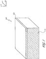
- Figure 1 is a perspective view of a partially formed semiconductor device 100 in which a transistor array is to be formed.
- the device 100 comprises a memory array, such as an array of DRAM cells, although in other embodiments the device 100 comprises an array of other types of memory cells, such as static memory cells, dynamic memory cells, extended data out (“EDO”) memory cells, EDO DRAM, electrically erasable programmable read only memory (“EEPROM”) cells, synchronous dynamic random access memory (“SDRAM”) cells, double data rate (“DDR”) SDRAM cells, synchronous link dynamic random access memory (“SLDRAM”) cells, video dynamic random access memory (“VDRAM”) cells, RDRAMO cells, static random access memory (“SRAM”) cells, phase change or programmable conductor random access memory (“PCRAM”) cells, magnetic random access memory (“MRAM”) cells, and flash memory cells.
- static memory cells such as an array of DRAM cells
- EDO DRAM extended data out
- EEPROM electrically erasable programmable read only memory
- SDRAM synchronous dynamic random access memory
- the device 100 includes a semiconductor substrate 110, which comprises one or more of a wide variety of suitable semiconductor materials.
- the semiconductor substrate 110 includes semiconductor structures that have been fabricated thereon, such as doped silicon platforms. While the illustrated semiconductor substrate 110 comprises an intrinsically doped monocrystalline silicon wafer in the illustrated embodiment, in other embodiments the semiconductor substrate 110 comprises other forms of semiconductor layers, which optionally include other active or operable portions of semiconductor devices.
- an epitaxial layer 104 is grown on the substrate 110.
- the epitaxial layer 104 is a semiconductor layer (for example, comprising silicon) grown on the substrate 110 by an epitaxial growth process that extends the crystal structure of the substrate 110.
- the epitaxial layer 104 has a thickness that is preferably between about 2 ⁇ m and about 6 ⁇ m, and more preferably between about 3 ⁇ m and about 5 ⁇ m. In embodiments wherein the epitaxial layer 104 is grown on the substrate 110 before the subsequent etching steps described herein, the epitaxial layer 104 is considered part of the substrate 110.
- the epitaxial layer 104 is heavily doped with a conductivity type that is opposite that of the substrate 110, thereby enabling the epitaxial layer 104 to serve as an active area for transistors formed thereover, as will be better understood from the final structures disclosed herein.
- the doped implant regions include a lightly doped p - region that is positioned underneath a heavily doped p + region.
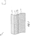
- Figure 2 illustrates a cross-section in the yz plane of the device of Figure 1 after deposition of additional layers over the substrate 110.
- the semiconductor device 100 further comprises an oxide layer 210 formed over the substrate 110 and the optional epitaxial layer 104.
- the oxide layer 210 is selectively etchable with respect to the material comprising the substrate 110 and silicon nitride.
- the oxide layer 210 comprises silicon dioxide and has a thickness that is preferably between about 100 ⁇ and 500 ⁇ , and more preferably between about 200 ⁇ and about 300 ⁇ .
- the oxide layer 210 is a pad oxide layer having a thickness of approximately 200 ⁇ .
- the oxide layer 210 is deposited using a suitable deposition process, such as chemical vapor deposition ("CVD") or physical vapor deposition (“PVD”), or is grown by oxidation of the underlying substrate.
- CVD chemical vapor deposition
- PVD physical vapor deposition
- the semiconductor device 100 further comprises a layer, such as the illustrated nitride layer 211, formed over the oxide layer 210.
- the nitride layer 211 comprises silicon nitride and has a thickness that is preferably between about 200 ⁇ and 2000 ⁇ , and more preferably between about 500 ⁇ and 1000 ⁇ .
- the nitride layer 211 is deposited using a suitable deposition process, such as CVD or PVD.
- the semiconductor device 100 further comprises a further hard mask layer 212 that is formed over the nitride layer 211.
- the hard mask layer 212 comprises amorphous carbon.
- the hard mask layer 212 comprises transparent carbon, tetraethylorthosilicate ("TEOS"), polycrystalline silicon, Si 3 N 4 , SiO x N y , SiC, or another suitable hard mask material.
- TEOS tetraethylorthosilicate
- the hard mask layer 212 is deposited using a suitable deposition process, such as CVD or PVD.
- the optional epitaxial layer 104 is omitted from subsequent illustrations.
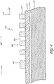
- Figure 3 illustrates a portion of a photo mask 300 to be applied to the device 100 to pattern the underlying hard mask layer 212.
- the shaded portion of the photo mask 300 represents the area in which the hard mask layer 212 will be removed after applying photolithography and etching techniques, and the unshaded portion represents the area in which the hard mask layer 212 will remain.
- the photo mask 300 is a clear field mask that is configured to define a pattern of active area lines 304 separated from each other by gaps 302 in an array region 308.
- the lines 304 and the gaps 302 are approximately 1100 ⁇ to approximately 1300 ⁇ wide.
- the lines 304 and the gaps 302 are approximately 1200 ⁇ wide.
- the photo mask 300 optionally includes a wider line 306 that is provided for optical proximity correction.
- the gaps 302 are used as a contact area for shallow trench isolation.
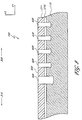
- Figure 4 illustrates a cross-section in the yz plane of the device of Figure 2 after applying the photo mask 300, illustrated in Figure 3 , to pattern the hard mask layer 212.
- the photo mask 300 is applied and transferred to the hard mask layer 212, such that the lines 304 and gaps 302 extend parallel to the x axis.
- the hard mask layer 212 remains over areas of the substrate 110 where the photo mask 300 forms lines 304, including the wider line 306, and is removed form areas of the substrate 110 where the photo mask 300 forms gaps 302.
- lines 304 and gaps 302 are located in an array region 308 of the device, which is surrounded by a periphery region 310 of the device.
- the hard mask layer 212 is patterned using photolithography and etching techniques.
- photoresist material is deposited as a blanket layer over the device 100, and is exposed to radiation through a reticle. Following this exposure, the photoresist material is developed to form the photo mask 300, illustrated in Figure 3 , on the surface of the hard mask layer 212.
- the hard mask layer 212 is then etched through the photo mask 300 to expose the nitride layer 211 of the device 100 in the gaps 302.
- Figure 5 illustrates a cross-section in the yz plane of the device of Figure 4 after blanket depositing a layer of spacer material 214 thereover.
- the spacer material 214 comprises an oxide material, such as silicon oxide having a thickness that is preferably between about 200 ⁇ and about 500 ⁇ , and more preferably between about 300 ⁇ and about 400 ⁇ .
- the spacer material 214 fills approximately 1/20 to approximately 1/3 of the horizontal dimension of the gaps 302.
- the spacer material 214 is deposited using a suitable deposition process, such as CVD or PVD.
- Figure 6 illustrates a cross-section in the yz plane of the device of Figure 5 after preferentially etching the spacer material 214 from horizontal surfaces in a directional spacer etch.
- the resulting structure includes spacers 216 positioned on the vertical sides of the lines 304.
- the spacers 216 which have a width approximately equal to the thickness of the original spacer material 214 deposition, effectively narrow the width of the gaps 302.
- the gaps 302 have a reduced width of between about 500 ⁇ and about 700 ⁇ after the spacers 216 are formed therein.
- the gaps 302 have a reduced width of about 600 ⁇ after the spacers 216 are formed therein.
- Figure 7 illustrates a cross-section in the yz plane of the device of Figure 6 after etching a plurality of deep trenches 400 through the nitride layer 211 and the oxide layer 210, and into the substrate 110.
- the pattern of deep trenches 400 is defined according to the gaps 302 between the spacers in the device array region 308.
- the deep trenches 400 are etched using a process such as ion milling, reactive ion etching ("RIE"), or chemical etching.
- RIE reactive ion etching
- RIE is a directional anisotropic etch having both physical and chemical components.
- a chemical etchant such as RIE
- a variety of etchants are usable, such as Cl 2 .
- the deep trenches 400 are etched to a depth of between about 3000 ⁇ and about 5000 ⁇ based on gaps 302, and are etched to a depth of between about 4000 ⁇ and about 5000 ⁇ adjacent to the wider line 306.
- the etching technique used to define the deep trenches causes the trench depth to be directly proportional to the trench width.
- Figure 8 illustrates a cross-section in the yz plane of the device of Figure 7 after filling the deep trenches 400 with a spin on dielectric ("SOD") material 408.
- SOD spin on dielectric
- An oxygen plasma technique is used to burn off the remaining hard mask layer 212, and a chemical mechanical polish (“CMP") technique is used to remove the remaining spacers 216 and excess SOD material.
- CMP chemical mechanical polish
- the CMP technique also provides the device 100 with a substantially planar surface 402 in the xy plane. As illustrated, the substantially planar surface 402 extends across the device array region 308 and periphery region 310.
- the deep trenches 400 are separated by remaining portions of the nitride layer 211; in a preferred embodiment, the deep trenches are separated by between approximately 1600 ⁇ and approximately 2000 ⁇ of nitride material. In an exemplary embodiment, the deep trenches 400 are separated by approximately 1800 ⁇ of nitride material. In another exemplary embodiment, the deep trenches 400 are separated by 2.25 ⁇ F , wherein F is the minimum resolvable feature size obtainable using a given photolithography technique.
- Figure 9 illustrates a cross-section in the yz plane of the device of Figure 8 after patterning another hard mask layer 312 over the deep trenches 400.
- the hard mask layer 312 is patterned based on a mask similar to that illustrated in Figure 3 , and is patterned using photolithography and etching techniques.
- the patterned hard mask layer 312 defines a plurality of lines 314 over the planar surface 402, with the lines 314 effectively masking the deep trenches 400.
- the lines 314 are separated by a plurality of gaps 318.
- the lines 314 are between about 1100 ⁇ and about 1300 ⁇ wide, and in an exemplary embodiment, the lines are approximately 1200 ⁇ wide.
- the lines 314 have substantially the same width as the lines 304 formed in the masking process illustrated in Figures 3 and 4 .
- Figure 10 illustrates a cross-section in the yz plane of the device of Figure 9 after forming a plurality of spacer loops 316 around the lines 314.
- the spacer loops 316 are formed by first depositing a blanket layer of spacer material over the structure illustrated in Figure 9 .
- the blanket spacer material comprises an oxide material, such as silicon oxide having a thickness that is preferably between about 200 ⁇ and about 500 ⁇ , and more preferably between about 300 ⁇ and about 400 ⁇ .
- the blanket layer of spacer material is deposited using a suitable deposition process, such as CVD or PVD.
- a directional spacer etch is then performed to remove the blanket spacer material from horizontal surfaces.
- the resulting structure is illustrated in Figure 10 .
- the spacer loops 316 which have a width approximately equal to the thickness of the original blanket spacer material deposition, effectively narrow the width of the gaps 318.
- the gaps 318 have a reduced width of between about 500 ⁇ and about 700 ⁇ after the spacer loops 316 are formed. In an exemplary embodiment, the gaps 318 have a reduced width of about 600 ⁇ after the spacer loops 316 are formed.
- Figure 11 illustrates a cross-section in the yz plane of the device of Figure 10 after etching a plurality of shallow trenches 404 through the nitride layer 211 and the oxide layer 210, and into the substrate 110.
- the shallow trenches 404 are formed parallel to the deep trenches 400.
- the shallow trenches 404 have substantially the same width as the deep trenches 400, but instead are etched to a reduced depth that is preferably between about 500 ⁇ and 2000 ⁇ , and more preferably between about 1000 ⁇ and 1500 ⁇ .
- Figure 12 illustrates a cross-section in the yz plane of the device of Figure 11 after filling the shallow trenches 404 with a SOD material 410.
- the shallow trenches are optionally filled with the same SOD material 408 used to fill the deep trenches 400.
- a CMP technique is used to remove the remaining hard mask layer 312, spacer loops 316, and excess SOD material.
- the CMP technique is used to reduce the thickness of the nitride layer 211 to between about 300 ⁇ and about 500 ⁇ .
- the CMP technique is used to reduce the thickness of the nitride layer 211 to about 400 ⁇ .
- the CMP technique also provides the device 100 with a substantially planar surface 406 in the xy plane.
- the substantially planar surface 406 extends across the device array region 308 and periphery region 310.
- Figure 13 illustrates a top-down view in the xy plane of the device 100 of Figure 12 .
- the device 100 illustrated in Figures 12 and 13 comprises a plurality of elongate shallow trenches 404 that are separated from each other by elongate nitride spacers with looped ends, as defined by the remaining nitride layer 211.
- the nitride spacers are separated from each other by the elongate deep trenches 400.
- the structure illustrated in Figures 12 and 13 is obtained using a process that self-aligns in the deep trenches 400 and the shallow trenches 404. As illustrated in Figure 25 , this self-alignment is achieved by first etching the nitride layer 211 in the array region 308. As illustrated in Figure 26 , nitride spacers 520 are then formed around the protruding SOD material 408 structures, which now act as mandrels. The nitride spacers 520 are then used to subsequently pattern shallow trenches, which are etched through the oxide layer 210 and into the substrate 110. The resulting structure is equivalent to the structure illustrated in Figures 12 and 13 , and is obtained without the use of the hard mask layer 312 illustrated in Figure 9 .
- Figure 14 illustrates a cross-section in the yz plane of the device of Figures 12 and 13 after removal of the remaining nitride layer 211 and oxide layer 210.
- the remaining portions of these layers are removed using an etching process, although other techniques are used in other embodiments.
- Subsequently performing a CMP technique results in a substantially planar surface of alternating silicon regions and oxide regions.
- the silicon regions define a plurality of elongate loops 112 that extend parallel to the x axis.
- the elongate loops 112 surround shallow trenches 404, and are separated from each other by the deep trenches 400.
- the elongate loops 112 are separated into individual transistor pillars by etching the loops perpendicular to their length, that is, parallel to the y axis.
- active devices are formed in the device periphery region 310 using the same masking sequence that is used to etch the elongate loops 112 into individual transistor pillars.
- active device layers are blanket deposited over the device illustrated in Figure 14 .
- the resulting structure is shown in Figure 15 , which illustrates a cross-section in the xz plane of the device of Figure 14 after forming an oxide layer 450, a polycrystalline silicon layer 452, and a tungsten silicide layer 454.
- the cross-section illustrated in Figure 15 illustrates these layers formed over a silicon region 114; however because these layers are blanket deposited, they also extend over the deep trenches 400 and the shallow trenches 402. Likewise, the blanket layers also extend over both the device array region 308 and periphery region 310.
- the blanket oxide layer 450 has a thickness between about 50 ⁇ and 80 ⁇ .
- other metallic materials are used in place of tungsten silicide to strap peripheral gates and improve lateral signal speed.
- an optional blanket silicon nitride layer (not shown) is formed over the tungsten silicide layer 454.
- the polycrystalline silicon layer 452 comprises a conductive material, wherein the term "conductive material" includes silicon, even if undoped as deposited.
- the tungsten silicon layer 454 is omitted, and is replaced with additional thickness of the polycrystalline silicon layer 452. This configuration advantageously removes metal from the structure, thereby reducing the likelihood of introducing contamination into other structures during subsequent processing. In such embodiments, the metal is added during a subsequent silicidation process.
- FIG. 16 illustrates a cross-section in the xz plane of the device of Figure 15 after patterning the blanket-deposited layers.
- the layers are patterned using photolithography and masking techniques.
- one or more active devices 460 are formed in the periphery region 310.
- the active devices comprise a stack including a gate oxide 462, a polycrystalline silicon active area 464, and a tungsten silicide strapping layer 466.
- the strapping layer 466 comprises other metallic materials, such as tungsten, titanium nitride, tantalum, and tantalum nitride. Mixtures of metals are also suitable for forming the strapping layer 466.
- the same photolithography and masking technique that is used to form active devices 460 in the periphery region is used to pattern a series of lines 470 in the array region 308.
- the array lines 470 comprise the same materials as the peripheral active devices 460, although the array lines 470 are used as a sacrificial mask to pattern the underlying elongate loops 112 in subsequent processing steps. Additionally, the pattern of lines 470 in the array region 308 has a smaller pitch as compared to the pattern of active devices 460 in the periphery region 310.
- the lines 470 are spaced apart by a spacing F, wherein the active devices 460 are spaced apart by a spacing 2 F , wherein F is the minimum resolvable feature size obtainable using a given photolithography technique.
- the active devices 460 have a spacing that is between about two times and about four times larger than the spacing for lines 470.
- the array lines 470 which extend parallel to the y axis, are perpendicular to the elongate loops 112, which extend parallel to the x axis.
- Figure 17 illustrates a cross-section in the xz plane of the device of Figure 16 after forming silicon nitride spacers 468 around the active devices 460 in the periphery region 310.
- the silicon nitride spacers 468 have a thickness of between about 200 ⁇ and about 800 ⁇ .
- the silicon nitride spacers 468 have a thickness of about 600 ⁇ , and are formed by blanket depositing silicon nitride over the device, followed by a directional etch that removes the deposited material from horizontal surfaces. This technique also results in silicon nitride spacers 468 being formed around the array lines 470 in the array region 308.
- the silicon nitride spacer material 468 fills the region between the lines, thereby forming a pattern of filled gaps 472 between the lines 470.
- An SOD material 474 such as silicon oxide, is formed in the regions of exposed silicon.
- a material other than silicon nitride is used to form the spacers and filled gaps; other suitable materials include materials that are selectively etched with respect to polycrystalline silicon and silicide materials.
- Figure 18 illustrates a cross-section in the xz plane of the device of Figure 17 after masking the device periphery region 310 and etching gate mandrels from the device.
- a mask 478 is formed over the periphery region 310 to protect the active devices 460 in the periphery region 310 during subsequent processing steps.
- the mask 478 is simple as it merely covers the periphery region 310 and opens the array 308, and therefore does not include "critical dimension" features.
- the remaining portions of the tungsten silicide layer 454 and the polycrystalline silicon layer 452 are etched from the exposed portions of the device, such as the array region 308.
- an etchant that is selective for polycrystalline silicon relative to oxide and nitride is used, such as tetramethylammonium hydroxide ("TMAH").
- TMAH tetramethylammonium hydroxide
- Other etchants are used in other embodiments. This results in the creation of trenches 476 between the nitride material of the filled gaps 472.
- the silicon is etched to the oxide layer 450, which acts as an etch stop.
- Figure 19 illustrates a cross-section in the xz plane of the device of Figure 18 after shrinking the remaining nitride portions of the filled gaps 472.
- this is accomplished by isotropically etching nitride from exposed portions of the device.
- the isotropic nitride etch advantageously creates an area of exposed silicon/dielectric 480 as the remainder of the filled gaps 472 are etched away from the remaining oxide layer 450.
- the remainder of the filled gaps 472 are etched to have a width corresponding to the width of the underlying silicon elongate loops 112, illustrated in Figure 14 .
- the remainder of the filled gaps 472 are etched to have a width of about 1/2F, where F is the minimum resolvable feature size obtainable using a given photolithography technique.
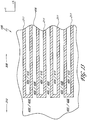
- Figure 20 illustrates a cross-section in the xz plane of the device of Figure 19 after etching the pattern of the trenches 476 into the underlying structure illustrated in Figure 14 .
- the trenches 476 are extended to an intermediate depth that is between the depth of the deep trenches 400 and the shallow trenches 404, illustrated in Figure 14 .
- the pattern of the intermediate trenches 476 is defined by the remaining nitride filled gaps 472. This effectively cuts the silicon elongate loops 112, the deep trenches 400, and the shallow trenches 404 to form a plurality of U-shaped transistor pillars.
- the shallow trenches 404 form the middle gap of the U-shaped transistor pillars.
- the U-shaped transistor pillars function source/drain regions for a U-shaped semiconductor structure.
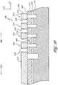
- Figure 21 illustrates a cross-section in the xz plane of the device of Figure 20 after removing excess nitride material and forming a plurality of sidewall spacers 482 in the intermediate trenches 476.
- the sidewall spacers 482 are separated from the silicon substrate 110 by a thin oxide layer 484, such as a thermal oxide.
- a portion of the substrate 110 corresponding to the region of the elongate loops 112 is doped to include a lightly doped n - region 486 that is positioned underneath a heavily doped n + region 488, although p-type doping can be employed in other embodiments.
- a lower portion of the elongate loops 112 is doped oppositely from an upper portion of the elongate loops 112.
- the sidewall spacers 482 have a width that is greater than or equal to half of a width of the elongate loops 112.
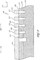
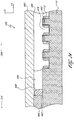
- Figure 22 provides a three-dimensional illustration of a portion of the partially-formed semiconductor device of Figure 21 .
- the device includes a plurality of transistor pillars that form the source 502 and drain 504 regions of a U-shaped transistor 500.
- the source 502 and drain 504 regions are separated by a shallow trench 404 which runs parallel to the x axis.
- the channel length of the transistor is the length extending from the source 502 to the drain 504 through the U-shaped channel region 506.
- the channel characteristics of the device are influenced by tailoring the dopant concentrations and types along the channel surfaces on opposite sides of the U-shaped protrusions.
- Neighboring U-shaped transistors 500 are separated from each other in the y dimension by deep trenches 400, and in the x dimension by lined with gate electrode sidewall spacers 482, which are positioned in the intermediate trenches.
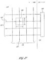
- Figure 27 schematically illustrates the dimensions of a memory cell 520 that is positioned in the array region 308 of a memory device.
- the memory cell 520 is located at the intersection of a selected bit line 522' in a bit line array 522 and a selected word line 524' in a word line array 524.
- the periphery region 310 of the memory device optionally includes logic circuitry 526 that is connected to the bit line array 522 and/or the word line array 524, as schematically illustrated in Figure 27 .
- the memory cell 520 occupies an area of the substrate 110 having dimensions x ⁇ y, and thus size of the memory cell is generally expressed as xyF 2 , where x and y are multiples of the minimum resolvable feature size F obtainable using a given photolithography technique, as described herein.
- the memory cell 520 typically comprises an access device (such as a transistor) and a storage device (such as a capacitor). In an unclaimed cross-point array, the access device can be omitted or an access device can be integrated with the storage device, as in MRAM, EEPROM or PCRAM (for example, silver-doped chalcogenide glass), where the status of a switch acts both as a switch and to store a memory state.
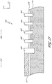
- the memory cell 520 is a DRAM cell employing the structure illustrated in Figure 23 .
- the structure illustrated in Figure 23 includes a single U-shaped transistor 500 having a source 502 and a drain 504 separated by a shallow trench 404.
- the source 502 and drain 504 are connected by a channel region 506, which is contiguous with the silicon substrate 110.
- This configuration advantageously avoids the floating body effect that is common in conventional vertical pillar transistors.
- Gate electrode sidewall spacers 482 are formed perpendicular to the shallow trench 404 and loop around both sides of the U-shaped semiconductor (silicon) protrusion.
- a capacitor 510 or other storage device is formed over the drain 504, and an insulated bit line 512 is formed over the source 502.
- the dimensions of the capacitor 510 and insulated bit line 512 are large compared to the dimensions of the pitch-doubled features of the U-shaped transistor 500.
- the overlying capacitor 510 and insulated bit line 512 advantageously accommodate a misalignment of up to 3 ⁇ 8 F , wherein F is the minimum resolvable feature size obtainable using a given photolithography technique.
- the memory cell 520 occupies a space on the substrate that is preferably between about 4 F 2 and about 8 F 2 , and is more preferably between about 4 F 2 and about 6.5 F 2 .
- the configuration of the U-shaped transistor 500 advantageously allows the dimensions of the transistors that forms a part of a memory cell to be independently scaled in the x and y dimensions, as illustrated in Figures 22 , 23 and 27 .
- this allows a memory cell occupying an area 6 F 2 on the substrate to be formed with a wide variety of different aspect ratios, including a 2.45 F ⁇ 2.45 F square, a 3 F ⁇ 2 F rectangle, and 2 F ⁇ 3 F rectangle.
- the aspect ratio of the transistors comprising the memory device is adjustable by manipulating the dimensions of the intermediate trenches 476 and the deep trenches 400 that separate the transistors.
- the capacitor 510 and insulated bit line 512 are used to interface the device 100 with other electronic circuitry of a larger system, including other devices which rely on memory such as computers and the like.
- computers optionally include processors, program logic, and/or other substrate configurations representing data and instructions.
- the processors optionally comprise controller circuitry, processor circuitry, processors, general purpose single chip or multiple chip microprocessors, digital signal processors, embedded microprocessors, microcontrollers and the like.
- the device 100 is able to be implemented in a wide variety of devices, products and systems.
- wafer contamination and refresh problems are addressed by eliminating the tungsten silicide layer 454 deposition illustrated in Figure 15 .
- the tungsten silicide layer 454 is replaced with an extended thickness polycrystalline silicon layer, illustrated as layer 464 in Figure 24 .
- an insulating layer 490 such as a SOD material, is blanket deposited over the array region 308.
- a CMP process is then performed to expose polycrystalline silicon 464 at the tops of the gate stacks in the device periphery region 310.
- a self-aligned silicidation process is then performed by first depositing a metal layer 492.
- a silicidation anneal is conducted to react the metal 492 (for example, titanium) in a self-aligned manner where it contacts the polycrystalline silicon layer 464.
- unreacted metal 492 can be selectively etched, as in known in the art.
- the exposed polycrystalline silicon is converted to titanium silicide.
- Other silicide materials such as tungsten silicide, ruthenium silicide, tantalum silicide, cobalt silicide or nickel silicide, are formed in other embodiments.
- This configuration advantageously allows the metal deposition step illustrated in Figure 15 to be eliminated, thereby reducing or eliminating metal contamination of the substrate and also simplifying removal of the sacrificial gate material (now just one layer of silicon) in the array 308.
- the embodiment of Figure 24 takes advantage of the fact that an insulating cap layer (for example, silicon nitride) is not needed for the peripheral transistors, because the dimensions of such transistors are not so tight as to require self-aligned contacts in the region 310.
- a three-sided U-shaped transistor is formed.
- the shallow trenches 404 are filled with a non-silicon oxide filler material, such as silicon nitride, at the stage of Figure 11 .
- a selective etch is used to remove the filler material from the shallow trenches 404.
- semiconductor material is also formed in the shallow trenches 404. Because the shallow trenches 404 are narrower than the intermediate trenches 476, the deposition of the sidewall spacers 482 fills the shallow trenches 404.
- the subsequent spacer etch merely recesses the gate material within the shallow trenches 404 below the level of the tops of the source/drain regions.
- This process creates a three-sided transistor structure.
- the gate material bridges the row of U-shaped protrusions forming the sidewall gate regions on both sides and equalizing potential. Additional details regarding this process are provided in Figures 32-35 and the corresponding written description of U.S. Patent Publication No. 2006/046407 A1 (Application No. 10/933,062 ).
- the fabrication techniques disclosed herein advantageously enable the forming of active devices in the periphery region and the patterning of intermediate trenches in the array region with a single mask.
- a second mask is used to separate the periphery and array regions for different subsequent processing steps.
- this second mask is not critical, and thus is easily aligned over existing structures on the substrate.
- the fabrication techniques disclosed herein are also applicable to other applications. For example, such techniques are usable to form single transistor, single capacitor DRAM cells.
- the same materials that are used to form active devices in the periphery region 310 are also used as sacrificial material for subsequent masking processes in the array region 300.
- examples of such materials include the polycrystalline silicon layer 452 and optionally, the tungsten silicide layer 454. This advantageously eliminates the need to use two different critical masks to separately form features in the device periphery region 310 and device array region 308.
- the material used to form the gate electrode sidewall spacers 482 In the device periphery region 310 is also used as a hard mask material in the device array region 308.
- deposition of the silicon nitride spacers 468 fill the gaps between the lines 470 in the array region 308.
Landscapes
- Engineering & Computer Science (AREA)
- Power Engineering (AREA)
- Microelectronics & Electronic Packaging (AREA)
- Manufacturing & Machinery (AREA)
- General Physics & Mathematics (AREA)
- Computer Hardware Design (AREA)
- Physics & Mathematics (AREA)
- Condensed Matter Physics & Semiconductors (AREA)
- Ceramic Engineering (AREA)
- Semiconductor Memories (AREA)
- Insulated Gate Type Field-Effect Transistor (AREA)
- Electrodes Of Semiconductors (AREA)
- Non-Volatile Memory (AREA)
Applications Claiming Priority (2)
| Application Number | Priority Date | Filing Date | Title |
|---|---|---|---|
| US11/366,212 US7476933B2 (en) | 2006-03-02 | 2006-03-02 | Vertical gated access transistor |
| PCT/US2007/005305 WO2007103147A2 (en) | 2006-03-02 | 2007-03-01 | U-shaped transistor and corresponding manufacturing method |
Publications (2)
| Publication Number | Publication Date |
|---|---|
| EP2011147A2 EP2011147A2 (en) | 2009-01-07 |
| EP2011147B1 true EP2011147B1 (en) | 2020-09-09 |
Family
ID=38377328
Family Applications (1)
| Application Number | Title | Priority Date | Filing Date |
|---|---|---|---|
| EP07752033.6A Active EP2011147B1 (en) | 2006-03-02 | 2007-03-01 | U-shaped access transistor and corresponding manufacturing method |
Country Status (6)
| Country | Link |
|---|---|
| US (5) | US7476933B2 (ja) |
| EP (1) | EP2011147B1 (ja) |
| JP (1) | JP5282888B2 (ja) |
| KR (1) | KR101364780B1 (ja) |
| CN (1) | CN101395714B (ja) |
| WO (1) | WO2007103147A2 (ja) |
Families Citing this family (59)
| Publication number | Priority date | Publication date | Assignee | Title |
|---|---|---|---|---|
| US7547945B2 (en) | 2004-09-01 | 2009-06-16 | Micron Technology, Inc. | Transistor devices, transistor structures and semiconductor constructions |
| US7282401B2 (en) | 2005-07-08 | 2007-10-16 | Micron Technology, Inc. | Method and apparatus for a self-aligned recessed access device (RAD) transistor gate |
| US7867851B2 (en) | 2005-08-30 | 2011-01-11 | Micron Technology, Inc. | Methods of forming field effect transistors on substrates |
| US7700441B2 (en) | 2006-02-02 | 2010-04-20 | Micron Technology, Inc. | Methods of forming field effect transistors, methods of forming field effect transistor gates, methods of forming integrated circuitry comprising a transistor gate array and circuitry peripheral to the gate array, and methods of forming integrated circuitry comprising a transistor gate array including first gates and second grounded isolation gates |
| US7897058B2 (en) * | 2006-02-13 | 2011-03-01 | Asml Netherlands B.V. | Device manufacturing method and computer program product |
| US7476933B2 (en) * | 2006-03-02 | 2009-01-13 | Micron Technology, Inc. | Vertical gated access transistor |
| US8852851B2 (en) | 2006-07-10 | 2014-10-07 | Micron Technology, Inc. | Pitch reduction technology using alternating spacer depositions during the formation of a semiconductor device and systems including same |
| US7602001B2 (en) * | 2006-07-17 | 2009-10-13 | Micron Technology, Inc. | Capacitorless one transistor DRAM cell, integrated circuitry comprising an array of capacitorless one transistor DRAM cells, and method of forming lines of capacitorless one transistor DRAM cells |
| US7772632B2 (en) | 2006-08-21 | 2010-08-10 | Micron Technology, Inc. | Memory arrays and methods of fabricating memory arrays |
| KR100791344B1 (ko) * | 2006-08-29 | 2008-01-03 | 삼성전자주식회사 | 반도체 집적 회로 장치의 제조 방법 |
| US7825460B2 (en) | 2006-09-06 | 2010-11-02 | International Business Machines Corporation | Vertical field effect transistor arrays and methods for fabrication thereof |
| US7589995B2 (en) | 2006-09-07 | 2009-09-15 | Micron Technology, Inc. | One-transistor memory cell with bias gate |
| US7859050B2 (en) * | 2007-01-22 | 2010-12-28 | Micron Technology, Inc. | Memory having a vertical access device |
| KR100881513B1 (ko) * | 2007-05-18 | 2009-02-05 | 주식회사 동부하이텍 | 반도체 미세패턴 형성 방법 |
| US7696040B2 (en) * | 2007-05-30 | 2010-04-13 | International Business Machines Corporation | Method for fabrication of fin memory structure |
| US7923373B2 (en) | 2007-06-04 | 2011-04-12 | Micron Technology, Inc. | Pitch multiplication using self-assembling materials |
| US7856613B1 (en) | 2008-01-30 | 2010-12-21 | Cadence Design Systems, Inc. | Method for self-aligned doubled patterning lithography |
| US8866254B2 (en) | 2008-02-19 | 2014-10-21 | Micron Technology, Inc. | Devices including fin transistors robust to gate shorts and methods of making the same |
| US7800965B2 (en) | 2008-03-10 | 2010-09-21 | Micron Technology, Inc. | Digit line equilibration using access devices at the edge of sub-arrays |
| US7989307B2 (en) | 2008-05-05 | 2011-08-02 | Micron Technology, Inc. | Methods of forming isolated active areas, trenches, and conductive lines in semiconductor structures and semiconductor structures including the same |
| US10151981B2 (en) * | 2008-05-22 | 2018-12-11 | Micron Technology, Inc. | Methods of forming structures supported by semiconductor substrates |
| US7824983B2 (en) * | 2008-06-02 | 2010-11-02 | Micron Technology, Inc. | Methods of providing electrical isolation in semiconductor structures |
| JP2009295785A (ja) * | 2008-06-05 | 2009-12-17 | Toshiba Corp | 半導体装置の製造方法 |
| US8101497B2 (en) | 2008-09-11 | 2012-01-24 | Micron Technology, Inc. | Self-aligned trench formation |
| CN101752225B (zh) * | 2008-12-04 | 2011-09-28 | 上海华虹Nec电子有限公司 | 超深沟槽的多级刻蚀与填充方法 |
| US8247302B2 (en) | 2008-12-04 | 2012-08-21 | Micron Technology, Inc. | Methods of fabricating substrates |
| US8273634B2 (en) | 2008-12-04 | 2012-09-25 | Micron Technology, Inc. | Methods of fabricating substrates |
| US8796155B2 (en) | 2008-12-04 | 2014-08-05 | Micron Technology, Inc. | Methods of fabricating substrates |
| KR101559063B1 (ko) * | 2009-02-02 | 2015-10-08 | 삼성전자주식회사 | 반도체 소자의 제조 방법 |
| US8692310B2 (en) | 2009-02-09 | 2014-04-08 | Spansion Llc | Gate fringing effect based channel formation for semiconductor device |
| US8268543B2 (en) | 2009-03-23 | 2012-09-18 | Micron Technology, Inc. | Methods of forming patterns on substrates |
| KR101561061B1 (ko) * | 2009-04-10 | 2015-10-16 | 삼성전자주식회사 | 돌출형 소자 분리막을 가지는 반도체 소자 |
| US9330934B2 (en) | 2009-05-18 | 2016-05-03 | Micron Technology, Inc. | Methods of forming patterns on substrates |
| CN102714142B (zh) * | 2009-10-26 | 2015-08-12 | 桑迪士克3D有限责任公司 | 采用用于四倍半节距凸起图案化的两次侧壁图案化形成存储器线和结构的设备和方法 |
| US8518788B2 (en) | 2010-08-11 | 2013-08-27 | Micron Technology, Inc. | Methods of forming a plurality of capacitors |
| US8455341B2 (en) | 2010-09-02 | 2013-06-04 | Micron Technology, Inc. | Methods of forming features of integrated circuitry |
| KR101723864B1 (ko) * | 2010-10-08 | 2017-04-07 | 삼성전자주식회사 | 수직 채널 트랜지스터를 구비하는 반도체 장치 및 그 제조 방법 |
| US8921899B2 (en) | 2010-11-19 | 2014-12-30 | Micron Technology, Inc. | Double gated 4F2 dram CHC cell and methods of fabricating the same |
| KR101205118B1 (ko) * | 2011-03-11 | 2012-11-26 | 에스케이하이닉스 주식회사 | 반도체 소자 및 그 제조 방법 |
| US8293615B2 (en) * | 2011-03-24 | 2012-10-23 | International Business Machines Corporation | Self-aligned dual depth isolation and method of fabrication |
| US9673102B2 (en) | 2011-04-01 | 2017-06-06 | Micron Technology, Inc. | Methods of forming vertical field-effect transistor with self-aligned contacts for memory devices with planar periphery/array and intermediate structures formed thereby |
| US8575032B2 (en) | 2011-05-05 | 2013-11-05 | Micron Technology, Inc. | Methods of forming a pattern on a substrate |
| US8648414B2 (en) | 2011-07-01 | 2014-02-11 | Micron Technology, Inc. | Semiconductor structures including bodies of semiconductor material, devices including such structures and related methods |
| US9076680B2 (en) | 2011-10-18 | 2015-07-07 | Micron Technology, Inc. | Integrated circuitry, methods of forming capacitors, and methods of forming integrated circuitry comprising an array of capacitors and circuitry peripheral to the array |
| US9177794B2 (en) | 2012-01-13 | 2015-11-03 | Micron Technology, Inc. | Methods of patterning substrates |
| US8912065B2 (en) * | 2012-06-15 | 2014-12-16 | Nanya Technology Corporation | Method of fabricating semiconductor device |
| US8629048B1 (en) | 2012-07-06 | 2014-01-14 | Micron Technology, Inc. | Methods of forming a pattern on a substrate |
| KR102013842B1 (ko) | 2013-02-08 | 2019-08-26 | 삼성전자주식회사 | 반도체 소자의 제조 방법 |
| US9023695B2 (en) * | 2013-03-14 | 2015-05-05 | Taiwan Semiconductor Manufacturing Company, Ltd. | Method of patterning features of a semiconductor device |
| DE112013007058B4 (de) * | 2013-06-28 | 2023-08-24 | Tahoe Research, Ltd. | Herstellung einer defektfreien finnenbasierten Vorrichtung in einem lateralen Epitaxieüberwachsungsgebiet |
| TWI530992B (zh) * | 2013-09-30 | 2016-04-21 | 華亞科技股份有限公司 | 以免光罩方式定義位元線溝槽之半導體基底及其製造方法 |
| US9508719B2 (en) | 2014-11-26 | 2016-11-29 | Taiwan Semiconductor Manufacturing Company, Ltd. | Fin field effect transistor (FinFET) device with controlled end-to-end critical dimension and method for forming the same |
| TWI638385B (zh) | 2015-03-31 | 2018-10-11 | 聯華電子股份有限公司 | 半導體裝置的圖案化結構及其製作方法 |
| US9548243B1 (en) * | 2015-06-30 | 2017-01-17 | International Business Machines Corporation | Self aligned via and pillar cut for at least a self aligned double pitch |
| US10388644B2 (en) | 2016-11-29 | 2019-08-20 | Taiwan Semiconductor Manufacturing Company, Ltd. | Method of manufacturing conductors and semiconductor device which includes conductors |
| US10439047B2 (en) * | 2018-02-14 | 2019-10-08 | Applied Materials, Inc. | Methods for etch mask and fin structure formation |
| US11189712B2 (en) | 2019-08-22 | 2021-11-30 | International Business Machines Corporation | Formation of vertical transport field-effect transistor structure having increased effective width |
| CN114420694A (zh) * | 2020-06-19 | 2022-04-29 | 福建省晋华集成电路有限公司 | 半导体存储器 |
| KR20220005723A (ko) * | 2020-07-07 | 2022-01-14 | 주식회사 프로텍 | 마스크를 이용하는 구리 필러 기판 본딩 방법 |
Family Cites Families (214)
| Publication number | Priority date | Publication date | Assignee | Title |
|---|---|---|---|---|
| US4234362A (en) | 1978-11-03 | 1980-11-18 | International Business Machines Corporation | Method for forming an insulator between layers of conductive material |
| US4508579A (en) | 1981-03-30 | 1985-04-02 | International Business Machines Corporation | Lateral device structures using self-aligned fabrication techniques |
| US4432132A (en) | 1981-12-07 | 1984-02-21 | Bell Telephone Laboratories, Incorporated | Formation of sidewall oxide layers by reactive oxygen ion etching to define submicron features |
| US4419809A (en) | 1981-12-30 | 1983-12-13 | International Business Machines Corporation | Fabrication process of sub-micrometer channel length MOSFETs |
| DE3242113A1 (de) | 1982-11-13 | 1984-05-24 | Ibm Deutschland Gmbh, 7000 Stuttgart | Verfahren zur herstellung einer duennen dielektrischen isolation in einem siliciumhalbleiterkoerper |
| US4716131A (en) | 1983-11-28 | 1987-12-29 | Nec Corporation | Method of manufacturing semiconductor device having polycrystalline silicon layer with metal silicide film |
| US4570325A (en) | 1983-12-16 | 1986-02-18 | Kabushiki Kaisha Toshiba | Manufacturing a field oxide region for a semiconductor device |
| US4984039A (en) | 1985-05-03 | 1991-01-08 | Texas Instruments Incorporated | Tapered trench structure and process |
| US4648937A (en) | 1985-10-30 | 1987-03-10 | International Business Machines Corporation | Method of preventing asymmetric etching of lines in sub-micrometer range sidewall images transfer |
| GB8528967D0 (en) | 1985-11-25 | 1986-01-02 | Plessey Co Plc | Semiconductor device manufacture |
| US5514885A (en) | 1986-10-09 | 1996-05-07 | Myrick; James J. | SOI methods and apparatus |
| US4838991A (en) | 1987-10-30 | 1989-06-13 | International Business Machines Corporation | Process for defining organic sidewall structures |
| US4776922A (en) | 1987-10-30 | 1988-10-11 | International Business Machines Corporation | Formation of variable-width sidewall structures |
| US5328810A (en) | 1990-05-07 | 1994-07-12 | Micron Technology, Inc. | Method for reducing, by a factor or 2-N, the minimum masking pitch of a photolithographic process |
| US5013680A (en) | 1990-07-18 | 1991-05-07 | Micron Technology, Inc. | Process for fabricating a DRAM array having feature widths that transcend the resolution limit of available photolithography |
| US5053105A (en) | 1990-07-19 | 1991-10-01 | Micron Technology, Inc. | Process for creating an etch mask suitable for deep plasma etches employing self-aligned silicidation of a metal layer masked with a silicon dioxide template |
| US5047117A (en) | 1990-09-26 | 1991-09-10 | Micron Technology, Inc. | Method of forming a narrow self-aligned, annular opening in a masking layer |
| DE4034612A1 (de) | 1990-10-31 | 1992-05-07 | Huels Chemische Werke Ag | Verfahren zur herstellung von methacryloxy- oder acryloxygruppen enthaltenden organosilanen |
| IT1243919B (it) | 1990-11-20 | 1994-06-28 | Cons Ric Microelettronica | Procedimento per l'ottenimento di solchi submicrometrici planarizzati in circuiti integrati realizzati con tecnologia ulsi |
| GB9105767D0 (en) * | 1991-03-19 | 1991-11-06 | British Aerospace | Wing root design of forward swept wings |
| US5208172A (en) | 1992-03-02 | 1993-05-04 | Motorola, Inc. | Method for forming a raised vertical transistor |
| US5315142A (en) | 1992-03-23 | 1994-05-24 | International Business Machines Corporation | High performance trench EEPROM cell |
| JPH05343370A (ja) | 1992-06-10 | 1993-12-24 | Toshiba Corp | 微細パタ−ンの形成方法 |
| US5330879A (en) | 1992-07-16 | 1994-07-19 | Micron Technology, Inc. | Method for fabrication of close-tolerance lines and sharp emission tips on a semiconductor wafer |
| JPH0677480A (ja) | 1992-08-24 | 1994-03-18 | Hitachi Ltd | 半導体装置 |
| US5319753A (en) | 1992-09-29 | 1994-06-07 | Zilog, Inc. | Queued interrupt mechanism with supplementary command/status/message information |
| DE4236609A1 (de) | 1992-10-29 | 1994-05-05 | Siemens Ag | Verfahren zur Erzeugung einer Struktur in der Oberfläche eines Substrats |
| US5407785A (en) | 1992-12-18 | 1995-04-18 | Vlsi Technology, Inc. | Method for generating dense lines on a semiconductor wafer using phase-shifting and multiple exposures |
| US5470661A (en) | 1993-01-07 | 1995-11-28 | International Business Machines Corporation | Diamond-like carbon films from a hydrocarbon helium plasma |
| JP3311070B2 (ja) * | 1993-03-15 | 2002-08-05 | 株式会社東芝 | 半導体装置 |
| JPH06318680A (ja) | 1993-05-10 | 1994-11-15 | Nec Corp | 半導体記憶装置およびその製造方法 |
| US6042998A (en) | 1993-09-30 | 2000-03-28 | The University Of New Mexico | Method and apparatus for extending spatial frequencies in photolithography images |
| KR970009054B1 (ko) | 1993-12-29 | 1997-06-03 | 현대전자산업 주식회사 | 평면구조 모스 트랜지스터 및 그 제조방법 |
| JP3720064B2 (ja) | 1994-01-20 | 2005-11-24 | 株式会社ルネサステクノロジ | 半導体集積回路 |
| JPH0855920A (ja) | 1994-08-15 | 1996-02-27 | Toshiba Corp | 半導体装置の製造方法 |
| JPH0855908A (ja) | 1994-08-17 | 1996-02-27 | Toshiba Corp | 半導体装置 |
| US5600153A (en) | 1994-10-07 | 1997-02-04 | Micron Technology, Inc. | Conductive polysilicon lines and thin film transistors |
| US5795830A (en) | 1995-06-06 | 1998-08-18 | International Business Machines Corporation | Reducing pitch with continuously adjustable line and space dimensions |
| KR100190757B1 (ko) | 1995-06-30 | 1999-06-01 | 김영환 | 모스 전계 효과 트랜지스터 형성방법 |
| JP3393286B2 (ja) | 1995-09-08 | 2003-04-07 | ソニー株式会社 | パターンの形成方法 |
| US5789320A (en) | 1996-04-23 | 1998-08-04 | International Business Machines Corporation | Plating of noble metal electrodes for DRAM and FRAM |
| JPH09293793A (ja) | 1996-04-26 | 1997-11-11 | Mitsubishi Electric Corp | 薄膜トランジスタを有する半導体装置およびその製造方法 |
| JP3164026B2 (ja) | 1996-08-21 | 2001-05-08 | 日本電気株式会社 | 半導体装置及びその製造方法 |
| US5989998A (en) | 1996-08-29 | 1999-11-23 | Matsushita Electric Industrial Co., Ltd. | Method of forming interlayer insulating film |
| US5817560A (en) | 1996-09-12 | 1998-10-06 | Advanced Micro Devices, Inc. | Ultra short trench transistors and process for making same |
| US5998256A (en) | 1996-11-01 | 1999-12-07 | Micron Technology, Inc. | Semiconductor processing methods of forming devices on a substrate, forming device arrays on a substrate, forming conductive lines on a substrate, and forming capacitor arrays on a substrate, and integrated circuitry |
| US6395613B1 (en) | 2000-08-30 | 2002-05-28 | Micron Technology, Inc. | Semiconductor processing methods of forming a plurality of capacitors on a substrate, bit line contacts and method of forming bit line contacts |
| US5679591A (en) | 1996-12-16 | 1997-10-21 | Taiwan Semiconductor Manufacturing Company, Ltd | Method of making raised-bitline contactless trenched flash memory cell |
| US6214727B1 (en) | 1997-02-11 | 2001-04-10 | Micron Technology, Inc. | Conductive electrical contacts, capacitors, DRAMs, and integrated circuitry, and methods of forming conductive electrical contacts, capacitors, DRAMs, and integrated circuitry |
| US5981333A (en) | 1997-02-11 | 1999-11-09 | Micron Technology, Inc. | Methods of forming capacitors and DRAM arrays |
| US6309975B1 (en) | 1997-03-14 | 2001-10-30 | Micron Technology, Inc. | Methods of making implanted structures |
| US6288431B1 (en) | 1997-04-04 | 2001-09-11 | Nippon Steel Corporation | Semiconductor device and a method of manufacturing the same |
| US6063688A (en) | 1997-09-29 | 2000-05-16 | Intel Corporation | Fabrication of deep submicron structures and quantum wire transistors using hard-mask transistor width definition |
| US6143476A (en) | 1997-12-12 | 2000-11-07 | Applied Materials Inc | Method for high temperature etching of patterned layers using an organic mask stack |
| DE59814170D1 (de) | 1997-12-17 | 2008-04-03 | Qimonda Ag | Speicherzellenanordnung und Verfahren zu deren Herstellung |
| US6291334B1 (en) | 1997-12-19 | 2001-09-18 | Applied Materials, Inc. | Etch stop layer for dual damascene process |
| US6004862A (en) | 1998-01-20 | 1999-12-21 | Advanced Micro Devices, Inc. | Core array and periphery isolation technique |
| JP2975917B2 (ja) | 1998-02-06 | 1999-11-10 | 株式会社半導体プロセス研究所 | 半導体装置の製造方法及び半導体装置の製造装置 |
| US5933725A (en) | 1998-05-27 | 1999-08-03 | Vanguard International Semiconductor Corporation | Word line resistance reduction method and design for high density memory with relaxed metal pitch |
| US6245662B1 (en) | 1998-07-23 | 2001-06-12 | Applied Materials, Inc. | Method of producing an interconnect structure for an integrated circuit |
| US6191444B1 (en) | 1998-09-03 | 2001-02-20 | Micron Technology, Inc. | Mini flash process and circuit |
| US6319782B1 (en) | 1998-09-10 | 2001-11-20 | Matsushita Electric Industrial Co., Ltd. | Semiconductor device and method of fabricating the same |
| US6333866B1 (en) | 1998-09-28 | 2001-12-25 | Texas Instruments Incorporated | Semiconductor device array having dense memory cell array and heirarchical bit line scheme |
| US6071789A (en) | 1998-11-10 | 2000-06-06 | Vanguard International Semiconductor Corporation | Method for simultaneously fabricating a DRAM capacitor and metal interconnections |
| DE19853268C2 (de) * | 1998-11-18 | 2002-04-11 | Infineon Technologies Ag | Feldeffektgesteuerter Transistor und Verfahren zu dessen Herstellung |
| US6271141B2 (en) | 1999-03-23 | 2001-08-07 | Micron Technology, Inc. | Methods of forming materials over uneven surface topologies, and methods of forming insulative materials over and between conductive lines |
| US6211044B1 (en) | 1999-04-12 | 2001-04-03 | Advanced Micro Devices | Process for fabricating a semiconductor device component using a selective silicidation reaction |
| US6159801A (en) | 1999-04-26 | 2000-12-12 | Taiwan Semiconductor Manufacturing Company | Method to increase coupling ratio of source to floating gate in split-gate flash |
| US6110837A (en) | 1999-04-28 | 2000-08-29 | Worldwide Semiconductor Manufacturing Corp. | Method for forming a hard mask of half critical dimension |
| US6136662A (en) | 1999-05-13 | 2000-10-24 | Lsi Logic Corporation | Semiconductor wafer having a layer-to-layer alignment mark and method for fabricating the same |
| DE19928781C1 (de) | 1999-06-23 | 2000-07-06 | Siemens Ag | DRAM-Zellenanordnung und Verfahren zu deren Herstellung |
| JP2001077196A (ja) | 1999-09-08 | 2001-03-23 | Sony Corp | 半導体装置の製造方法 |
| US6282113B1 (en) | 1999-09-29 | 2001-08-28 | International Business Machines Corporation | Four F-squared gapless dual layer bitline DRAM array architecture |
| US6362057B1 (en) | 1999-10-26 | 2002-03-26 | Motorola, Inc. | Method for forming a semiconductor device |
| US6582891B1 (en) | 1999-12-02 | 2003-06-24 | Axcelis Technologies, Inc. | Process for reducing edge roughness in patterned photoresist |
| KR100311050B1 (ko) | 1999-12-14 | 2001-11-05 | 윤종용 | 커패시터의 전극 제조 방법 |
| JP2001175073A (ja) * | 1999-12-14 | 2001-06-29 | Canon Inc | 現像剤担持体、現像装置及びプロセスカートリッジ並びに画像形成装置 |
| US6573030B1 (en) | 2000-02-17 | 2003-06-03 | Applied Materials, Inc. | Method for depositing an amorphous carbon layer |
| US6967140B2 (en) | 2000-03-01 | 2005-11-22 | Intel Corporation | Quantum wire gate device and method of making same |
| US6297554B1 (en) | 2000-03-10 | 2001-10-02 | United Microelectronics Corp. | Dual damascene interconnect structure with reduced parasitic capacitance |
| US6423474B1 (en) | 2000-03-21 | 2002-07-23 | Micron Technology, Inc. | Use of DARC and BARC in flash memory processing |
| JP3805603B2 (ja) | 2000-05-29 | 2006-08-02 | 富士通株式会社 | 半導体装置及びその製造方法 |
| US6431887B1 (en) | 2000-05-31 | 2002-08-13 | Tyco Electronics Corporation | Electrical connector assembly with an EMI shielded plug and grounding latch member |
| US6632741B1 (en) | 2000-07-19 | 2003-10-14 | International Business Machines Corporation | Self-trimming method on looped patterns |
| US6455372B1 (en) | 2000-08-14 | 2002-09-24 | Micron Technology, Inc. | Nucleation for improved flash erase characteristics |
| US6348380B1 (en) | 2000-08-25 | 2002-02-19 | Micron Technology, Inc. | Use of dilute steam ambient for improvement of flash devices |
| SE517275C2 (sv) | 2000-09-20 | 2002-05-21 | Obducat Ab | Sätt vid våtetsning av ett substrat |
| US6335257B1 (en) | 2000-09-29 | 2002-01-01 | Vanguard International Semiconductor Corporation | Method of making pillar-type structure on semiconductor substrate |
| US6340614B1 (en) | 2000-10-03 | 2002-01-22 | Vanguard International Semiconductor Corporation | Method of forming a DRAM cell |
| US6483154B1 (en) * | 2000-10-05 | 2002-11-19 | Advanced Micro Devices, Inc. | Nitrogen oxide plasma treatment for reduced nickel silicide bridging |
| US6667237B1 (en) | 2000-10-12 | 2003-12-23 | Vram Technologies, Llc | Method and apparatus for patterning fine dimensions |
| JP2002124585A (ja) | 2000-10-17 | 2002-04-26 | Hitachi Ltd | 不揮発性半導体記憶装置およびその製造方法 |
| US6534243B1 (en) | 2000-10-23 | 2003-03-18 | Advanced Micro Devices, Inc. | Chemical feature doubling process |
| US6926843B2 (en) | 2000-11-30 | 2005-08-09 | International Business Machines Corporation | Etching of hard masks |
| US6664028B2 (en) | 2000-12-04 | 2003-12-16 | United Microelectronics Corp. | Method of forming opening in wafer layer |
| JP2002203913A (ja) | 2000-12-28 | 2002-07-19 | Hitachi Ltd | 半導体記憶装置の製造方法および半導体記憶装置 |
| US6531727B2 (en) | 2001-02-09 | 2003-03-11 | Micron Technology, Inc. | Open bit line DRAM with ultra thin body transistors |
| US6424001B1 (en) | 2001-02-09 | 2002-07-23 | Micron Technology, Inc. | Flash memory with ultra thin vertical body transistors |
| US6597203B2 (en) | 2001-03-14 | 2003-07-22 | Micron Technology, Inc. | CMOS gate array with vertical transistors |
| US6545904B2 (en) | 2001-03-16 | 2003-04-08 | Micron Technology, Inc. | 6f2 dram array, a dram array formed on a semiconductive substrate, a method of forming memory cells in a 6f2 dram array and a method of isolating a single row of memory cells in a 6f2 dram array |
| US7176109B2 (en) | 2001-03-23 | 2007-02-13 | Micron Technology, Inc. | Method for forming raised structures by controlled selective epitaxial growth of facet using spacer |
| US6475867B1 (en) | 2001-04-02 | 2002-11-05 | Advanced Micro Devices, Inc. | Method of forming integrated circuit features by oxidation of titanium hard mask |
| US6548347B2 (en) | 2001-04-12 | 2003-04-15 | Micron Technology, Inc. | Method of forming minimally spaced word lines |
| US6740594B2 (en) | 2001-05-31 | 2004-05-25 | Infineon Technologies Ag | Method for removing carbon-containing polysilane from a semiconductor without stripping |
| US6960806B2 (en) | 2001-06-21 | 2005-11-01 | International Business Machines Corporation | Double gated vertical transistor with different first and second gate materials |
| US6737333B2 (en) * | 2001-07-03 | 2004-05-18 | Texas Instruments Incorporated | Semiconductor device isolation structure and method of forming |
| JP2003031686A (ja) | 2001-07-16 | 2003-01-31 | Sony Corp | 半導体記憶装置およびその製造方法 |
| US6522584B1 (en) | 2001-08-02 | 2003-02-18 | Micron Technology, Inc. | Programming methods for multi-level flash EEPROMs |
| US6599684B2 (en) | 2001-08-13 | 2003-07-29 | Eastman Kodak Company | Color photothermographic element comprising a dye-forming system for forming a novel infrared dye |
| US6744094B2 (en) | 2001-08-24 | 2004-06-01 | Micron Technology Inc. | Floating gate transistor with horizontal gate layers stacked next to vertical body |
| TW497138B (en) | 2001-08-28 | 2002-08-01 | Winbond Electronics Corp | Method for improving consistency of critical dimension |
| DE10142590A1 (de) | 2001-08-31 | 2003-04-03 | Infineon Technologies Ag | Verfahren zur Seitenwandverstärkung von Resiststrukturen und zur Herstellung von Strukturen mit reduzierter Strukturgröße |
| JP2003133437A (ja) | 2001-10-24 | 2003-05-09 | Hitachi Ltd | 半導体装置の製造方法および半導体装置 |
| JP2003168749A (ja) | 2001-12-03 | 2003-06-13 | Hitachi Ltd | 不揮発性半導体記憶装置及びその製造方法 |
| US7226853B2 (en) | 2001-12-26 | 2007-06-05 | Applied Materials, Inc. | Method of forming a dual damascene structure utilizing a three layer hard mask structure |
| TW576864B (en) | 2001-12-28 | 2004-02-21 | Toshiba Corp | Method for manufacturing a light-emitting device |
| US6638441B2 (en) | 2002-01-07 | 2003-10-28 | Macronix International Co., Ltd. | Method for pitch reduction |
| DE10207131B4 (de) | 2002-02-20 | 2007-12-20 | Infineon Technologies Ag | Verfahren zur Bildung einer Hartmaske in einer Schicht auf einer flachen Scheibe |
| US6759180B2 (en) | 2002-04-23 | 2004-07-06 | Hewlett-Packard Development Company, L.P. | Method of fabricating sub-lithographic sized line and space patterns for nano-imprinting lithography |
| US6806123B2 (en) | 2002-04-26 | 2004-10-19 | Micron Technology, Inc. | Methods of forming isolation regions associated with semiconductor constructions |
| US20030207584A1 (en) | 2002-05-01 | 2003-11-06 | Swaminathan Sivakumar | Patterning tighter and looser pitch geometries |
| US6951709B2 (en) | 2002-05-03 | 2005-10-04 | Micron Technology, Inc. | Method of fabricating a semiconductor multilevel interconnect structure |
| US6602779B1 (en) | 2002-05-13 | 2003-08-05 | Taiwan Semiconductor Manufacturing Co., Ltd | Method for forming low dielectric constant damascene structure while employing carbon doped silicon oxide planarizing stop layer |
| US6900521B2 (en) | 2002-06-10 | 2005-05-31 | Micron Technology, Inc. | Vertical transistors and output prediction logic circuits containing same |
| US6734107B2 (en) | 2002-06-12 | 2004-05-11 | Macronix International Co., Ltd. | Pitch reduction in semiconductor fabrication |
| US6559017B1 (en) | 2002-06-13 | 2003-05-06 | Advanced Micro Devices, Inc. | Method of using amorphous carbon as spacer material in a disposable spacer process |
| KR100476924B1 (ko) | 2002-06-14 | 2005-03-17 | 삼성전자주식회사 | 반도체 장치의 미세 패턴 형성 방법 |
| US6777725B2 (en) * | 2002-06-14 | 2004-08-17 | Ingentix Gmbh & Co. Kg | NROM memory circuit with recessed bitline |
| US6924191B2 (en) | 2002-06-20 | 2005-08-02 | Applied Materials, Inc. | Method for fabricating a gate structure of a field effect transistor |
| US20030235076A1 (en) | 2002-06-21 | 2003-12-25 | Micron Technology, Inc. | Multistate NROM having a storage density much greater than 1 Bit per 1F2 |
| WO2004003977A2 (en) | 2002-06-27 | 2004-01-08 | Advanced Micro Devices, Inc. | Method of defining the dimensions of circuit elements by using spacer deposition techniques |
| US6835663B2 (en) | 2002-06-28 | 2004-12-28 | Infineon Technologies Ag | Hardmask of amorphous carbon-hydrogen (a-C:H) layers with tunable etch resistivity |
| US6689695B1 (en) | 2002-06-28 | 2004-02-10 | Taiwan Semiconductor Manufacturing Company | Multi-purpose composite mask for dual damascene patterning |
| US20040018738A1 (en) | 2002-07-22 | 2004-01-29 | Wei Liu | Method for fabricating a notch gate structure of a field effect transistor |
| US6734063B2 (en) | 2002-07-22 | 2004-05-11 | Infineon Technologies Ag | Non-volatile memory cell and fabrication method |
| US6913871B2 (en) | 2002-07-23 | 2005-07-05 | Intel Corporation | Fabricating sub-resolution structures in planar lightwave devices |
| US6764949B2 (en) | 2002-07-31 | 2004-07-20 | Advanced Micro Devices, Inc. | Method for reducing pattern deformation and photoresist poisoning in semiconductor device fabrication |
| US6673684B1 (en) | 2002-07-31 | 2004-01-06 | Advanced Micro Devices, Inc. | Use of diamond as a hard mask material |
| US6800930B2 (en) | 2002-07-31 | 2004-10-05 | Micron Technology, Inc. | Semiconductor dice having back side redistribution layer accessed using through-silicon vias, and assemblies |
| US6939808B2 (en) | 2002-08-02 | 2005-09-06 | Applied Materials, Inc. | Undoped and fluorinated amorphous carbon film as pattern mask for metal etch |
| US7071043B2 (en) | 2002-08-15 | 2006-07-04 | Micron Technology, Inc. | Methods of forming a field effect transistor having source/drain material over insulative material |
| US6888187B2 (en) | 2002-08-26 | 2005-05-03 | International Business Machines Corporation | DRAM cell with enhanced SER immunity |
| US6566280B1 (en) | 2002-08-26 | 2003-05-20 | Intel Corporation | Forming polymer features on a substrate |
| US7205598B2 (en) | 2002-08-29 | 2007-04-17 | Micron Technology, Inc. | Random access memory device utilizing a vertically oriented select transistor |
| US6794699B2 (en) | 2002-08-29 | 2004-09-21 | Micron Technology Inc | Annular gate and technique for fabricating an annular gate |
| US6756284B2 (en) | 2002-09-18 | 2004-06-29 | Silicon Storage Technology, Inc. | Method for forming a sublithographic opening in a semiconductor process |
| US6706571B1 (en) | 2002-10-22 | 2004-03-16 | Advanced Micro Devices, Inc. | Method for forming multiple structures in a semiconductor device |
| US6888755B2 (en) | 2002-10-28 | 2005-05-03 | Sandisk Corporation | Flash memory cell arrays having dual control gates per memory cell charge storage element |
| US6804142B2 (en) * | 2002-11-12 | 2004-10-12 | Micron Technology, Inc. | 6F2 3-transistor DRAM gain cell |
| US7119020B2 (en) | 2002-12-04 | 2006-10-10 | Matsushita Electric Industrial Co., Ltd. | Method for fabricating semiconductor device |
| US6686245B1 (en) | 2002-12-20 | 2004-02-03 | Motorola, Inc. | Vertical MOSFET with asymmetric gate structure |
| JP2004214379A (ja) * | 2002-12-27 | 2004-07-29 | Toshiba Corp | 半導体装置、ダイナミック型半導体記憶装置及び半導体装置の製造方法 |
| US7304336B2 (en) | 2003-02-13 | 2007-12-04 | Massachusetts Institute Of Technology | FinFET structure and method to make the same |
| DE10362018B4 (de) | 2003-02-14 | 2007-03-08 | Infineon Technologies Ag | Anordnung und Verfahren zur Herstellung von vertikalen Transistorzellen und transistorgesteuerten Speicherzellen |
| US7084076B2 (en) | 2003-02-27 | 2006-08-01 | Samsung Electronics, Co., Ltd. | Method for forming silicon dioxide film using siloxane |
| US7015124B1 (en) | 2003-04-28 | 2006-03-21 | Advanced Micro Devices, Inc. | Use of amorphous carbon for gate patterning |
| US6773998B1 (en) | 2003-05-20 | 2004-08-10 | Advanced Micro Devices, Inc. | Modified film stack and patterning strategy for stress compensation and prevention of pattern distortion in amorphous carbon gate patterning |
| JP4578785B2 (ja) | 2003-05-21 | 2010-11-10 | ルネサスエレクトロニクス株式会社 | 半導体装置の製造方法 |
| KR100511045B1 (ko) * | 2003-07-14 | 2005-08-30 | 삼성전자주식회사 | 리세스된 게이트 전극을 갖는 반도체 소자의 집적방법 |
| US6835662B1 (en) | 2003-07-14 | 2004-12-28 | Advanced Micro Devices, Inc. | Partially de-coupled core and periphery gate module process |
| DE10332725A1 (de) | 2003-07-18 | 2005-02-24 | Forschungszentrum Jülich GmbH | Verfahren zur selbstjustierenden Verkleinerung von Strukturen |
| US6972988B1 (en) | 2003-08-08 | 2005-12-06 | Micron Technology, Inc. | State save-on-power-down using GMR non-volatile elements |
| US7105431B2 (en) | 2003-08-22 | 2006-09-12 | Micron Technology, Inc. | Masking methods |
| US6844591B1 (en) | 2003-09-17 | 2005-01-18 | Micron Technology, Inc. | Method of forming DRAM access transistors |
| DE10345455A1 (de) | 2003-09-30 | 2005-05-04 | Infineon Technologies Ag | Verfahren zum Erzeugen einer Hartmaske und Hartmasken-Anordnung |
| KR100536801B1 (ko) | 2003-10-01 | 2005-12-14 | 동부아남반도체 주식회사 | 반도체 소자 및 그 제조 방법 |
| US6867116B1 (en) | 2003-11-10 | 2005-03-15 | Macronix International Co., Ltd. | Fabrication method of sub-resolution pitch for integrated circuits |
| DE10361695B3 (de) * | 2003-12-30 | 2005-02-03 | Infineon Technologies Ag | Transistorstruktur mit gekrümmtem Kanal, Speicherzelle und Speicherzellenfeld für DRAMs sowie Verfahren zur Herstellung eines DRAMs |
| US6998332B2 (en) | 2004-01-08 | 2006-02-14 | International Business Machines Corporation | Method of independent P and N gate length control of FET device made by sidewall image transfer technique |
| US6875703B1 (en) | 2004-01-20 | 2005-04-05 | International Business Machines Corporation | Method for forming quadruple density sidewall image transfer (SIT) structures |
| US7372091B2 (en) | 2004-01-27 | 2008-05-13 | Micron Technology, Inc. | Selective epitaxy vertical integrated circuit components |
| US7064078B2 (en) | 2004-01-30 | 2006-06-20 | Applied Materials | Techniques for the use of amorphous carbon (APF) for various etch and litho integration scheme |
| KR100577565B1 (ko) | 2004-02-23 | 2006-05-08 | 삼성전자주식회사 | 핀 전계효과 트랜지스터의 제조방법 |
| US7030012B2 (en) | 2004-03-10 | 2006-04-18 | International Business Machines Corporation | Method for manufacturing tungsten/polysilicon word line structure in vertical DRAM |
| WO2005094231A2 (en) | 2004-03-19 | 2005-10-13 | The Regents Of The University Of California | Methods for fabrication of positional and compositionally controlled nanostructures on substrate |
| US7098105B2 (en) | 2004-05-26 | 2006-08-29 | Micron Technology, Inc. | Methods for forming semiconductor structures |
| US7183205B2 (en) | 2004-06-08 | 2007-02-27 | Macronix International Co., Ltd. | Method of pitch dimension shrinkage |
| US7473644B2 (en) | 2004-07-01 | 2009-01-06 | Micron Technology, Inc. | Method for forming controlled geometry hardmasks including subresolution elements |
| DE102004036461A1 (de) * | 2004-07-28 | 2006-02-16 | Infineon Technologies Ag | Elektronische Datenspeichervorrichtung für hohen Lesestrom |
| KR100704470B1 (ko) | 2004-07-29 | 2007-04-10 | 주식회사 하이닉스반도체 | 비결정성 탄소막을 희생 하드마스크로 이용하는반도체소자 제조 방법 |
| US7151040B2 (en) | 2004-08-31 | 2006-12-19 | Micron Technology, Inc. | Methods for increasing photo alignment margins |
| US7442976B2 (en) * | 2004-09-01 | 2008-10-28 | Micron Technology, Inc. | DRAM cells with vertical transistors |
| US7910288B2 (en) | 2004-09-01 | 2011-03-22 | Micron Technology, Inc. | Mask material conversion |
| US7115525B2 (en) | 2004-09-02 | 2006-10-03 | Micron Technology, Inc. | Method for integrated circuit fabrication using pitch multiplication |
| US7655387B2 (en) | 2004-09-02 | 2010-02-02 | Micron Technology, Inc. | Method to align mask patterns |
| KR100614651B1 (ko) * | 2004-10-11 | 2006-08-22 | 삼성전자주식회사 | 회로 패턴의 노광을 위한 장치 및 방법, 사용되는포토마스크 및 그 설계 방법, 그리고 조명계 및 그 구현방법 |
| US7208379B2 (en) | 2004-11-29 | 2007-04-24 | Texas Instruments Incorporated | Pitch multiplication process |
| KR100596795B1 (ko) | 2004-12-16 | 2006-07-05 | 주식회사 하이닉스반도체 | 반도체 소자의 캐패시터 및 그 형성방법 |
| US7271107B2 (en) | 2005-02-03 | 2007-09-18 | Lam Research Corporation | Reduction of feature critical dimensions using multiple masks |
| US7323379B2 (en) | 2005-02-03 | 2008-01-29 | Mosys, Inc. | Fabrication process for increased capacitance in an embedded DRAM memory |
| US7253118B2 (en) * | 2005-03-15 | 2007-08-07 | Micron Technology, Inc. | Pitch reduced patterns relative to photolithography features |
| US7431927B2 (en) * | 2005-03-24 | 2008-10-07 | Epitomics, Inc. | TNFα-neutralizing antibodies |
| US7611944B2 (en) | 2005-03-28 | 2009-11-03 | Micron Technology, Inc. | Integrated circuit fabrication |
| KR100640639B1 (ko) | 2005-04-19 | 2006-10-31 | 삼성전자주식회사 | 미세콘택을 포함하는 반도체소자 및 그 제조방법 |
| US7429536B2 (en) | 2005-05-23 | 2008-09-30 | Micron Technology, Inc. | Methods for forming arrays of small, closely spaced features |
| US7547599B2 (en) | 2005-05-26 | 2009-06-16 | Micron Technology, Inc. | Multi-state memory cell |
| US7560390B2 (en) | 2005-06-02 | 2009-07-14 | Micron Technology, Inc. | Multiple spacer steps for pitch multiplication |
| US7396781B2 (en) | 2005-06-09 | 2008-07-08 | Micron Technology, Inc. | Method and apparatus for adjusting feature size and position |
| US7541632B2 (en) * | 2005-06-14 | 2009-06-02 | Micron Technology, Inc. | Relaxed-pitch method of aligning active area to digit line |
| US7413981B2 (en) | 2005-07-29 | 2008-08-19 | Micron Technology, Inc. | Pitch doubled circuit layout |
| US7291560B2 (en) | 2005-08-01 | 2007-11-06 | Infineon Technologies Ag | Method of production pitch fractionizations in semiconductor technology |
| US7816262B2 (en) | 2005-08-30 | 2010-10-19 | Micron Technology, Inc. | Method and algorithm for random half pitched interconnect layout with constant spacing |
| US7829262B2 (en) | 2005-08-31 | 2010-11-09 | Micron Technology, Inc. | Method of forming pitch multipled contacts |
| US7572572B2 (en) | 2005-09-01 | 2009-08-11 | Micron Technology, Inc. | Methods for forming arrays of small, closely spaced features |
| US7759197B2 (en) | 2005-09-01 | 2010-07-20 | Micron Technology, Inc. | Method of forming isolated features using pitch multiplication |
| US7776744B2 (en) | 2005-09-01 | 2010-08-17 | Micron Technology, Inc. | Pitch multiplication spacers and methods of forming the same |
| US7393789B2 (en) | 2005-09-01 | 2008-07-01 | Micron Technology, Inc. | Protective coating for planarization |
| US7687342B2 (en) | 2005-09-01 | 2010-03-30 | Micron Technology, Inc. | Method of manufacturing a memory device |
| US8716772B2 (en) * | 2005-12-28 | 2014-05-06 | Micron Technology, Inc. | DRAM cell design with folded digitline sense amplifier |
| US7842558B2 (en) | 2006-03-02 | 2010-11-30 | Micron Technology, Inc. | Masking process for simultaneously patterning separate regions |
| US7476933B2 (en) * | 2006-03-02 | 2009-01-13 | Micron Technology, Inc. | Vertical gated access transistor |
| US20070210449A1 (en) | 2006-03-07 | 2007-09-13 | Dirk Caspary | Memory device and an array of conductive lines and methods of making the same |
| US7537866B2 (en) | 2006-05-24 | 2009-05-26 | Synopsys, Inc. | Patterning a single integrated circuit layer using multiple masks and multiple masking layers |
| US8129289B2 (en) | 2006-10-05 | 2012-03-06 | Micron Technology, Inc. | Method to deposit conformal low temperature SiO2 |
-
2006
- 2006-03-02 US US11/366,212 patent/US7476933B2/en active Active
-
2007
- 2007-03-01 EP EP07752033.6A patent/EP2011147B1/en active Active
- 2007-03-01 KR KR1020087024116A patent/KR101364780B1/ko active IP Right Grant
- 2007-03-01 CN CN2007800071397A patent/CN101395714B/zh active Active
- 2007-03-01 WO PCT/US2007/005305 patent/WO2007103147A2/en active Application Filing
- 2007-03-01 JP JP2008557387A patent/JP5282888B2/ja active Active
-
2008
- 2008-11-26 US US12/324,701 patent/US7736980B2/en active Active
-
2010
- 2010-05-24 US US12/785,712 patent/US8039348B2/en active Active
-
2011
- 2011-10-13 US US13/272,679 patent/US8592898B2/en active Active
-
2013
- 2013-11-21 US US14/086,147 patent/US9184161B2/en active Active
Non-Patent Citations (1)
| Title |
|---|
| M. SAKAO: "A STRAIGHT-LINE-TRENCH ISOLATION AND TRENCH-GATE TRANSISTOR (SLIT) CELL FOR GIGA-BIT DRAMS", DIGEST OF TECHNICAL PAPERS OF THE SYMPOSIUM ON VLSI TECHNOLOGY, 17 May 1993 (1993-05-17), pages 19 - 20, XP010330186 * |
Also Published As
| Publication number | Publication date |
|---|---|
| CN101395714B (zh) | 2013-06-05 |
| US8039348B2 (en) | 2011-10-18 |
| US20100230733A1 (en) | 2010-09-16 |
| US9184161B2 (en) | 2015-11-10 |
| US8592898B2 (en) | 2013-11-26 |
| CN101395714A (zh) | 2009-03-25 |
| JP2009528701A (ja) | 2009-08-06 |
| US20090104744A1 (en) | 2009-04-23 |
| EP2011147A2 (en) | 2009-01-07 |
| JP5282888B2 (ja) | 2013-09-04 |
| US20070205443A1 (en) | 2007-09-06 |
| WO2007103147A3 (en) | 2007-11-01 |
| KR101364780B1 (ko) | 2014-02-21 |
| WO2007103147A2 (en) | 2007-09-13 |
| US7736980B2 (en) | 2010-06-15 |
| KR20090003303A (ko) | 2009-01-09 |
| US20120049246A1 (en) | 2012-03-01 |
| US20140077295A1 (en) | 2014-03-20 |
| US7476933B2 (en) | 2009-01-13 |
Similar Documents
| Publication | Publication Date | Title |
|---|---|---|
| EP2011147B1 (en) | U-shaped access transistor and corresponding manufacturing method | |
| US8772840B2 (en) | Memory device comprising an array portion and a logic portion | |
| EP1794791B1 (en) | Dram cells with vertical u-shaped transistors | |
| US8415738B2 (en) | Semiconductor memory device and manufacturing method thereof | |
| JP4233953B2 (ja) | 垂直型動的ランダム・アクセス・メモリ(dram)・アレイと論理回路部を含む複合型集積回路を作製する方法 | |
| KR100673673B1 (ko) | Dram 셀 장치 및 그 제조 방법 | |
| TW201909341A (zh) | 記憶元件及其製造方法 |
Legal Events
| Date | Code | Title | Description |
|---|---|---|---|
| PUAI | Public reference made under article 153(3) epc to a published international application that has entered the european phase |
Free format text: ORIGINAL CODE: 0009012 |
|
| 17P | Request for examination filed |
Effective date: 20081001 |
|
| AK | Designated contracting states |
Kind code of ref document: A2 Designated state(s): AT BE BG CH CY CZ DE DK EE ES FI FR GB GR HU IE IS IT LI LT LU LV MC MT NL PL PT RO SE SI SK TR |
|
| AX | Request for extension of the european patent |
Extension state: AL BA HR MK RS |
|
| RBV | Designated contracting states (corrected) |
Designated state(s): DE FR GB IT NL |
|
| 17Q | First examination report despatched |
Effective date: 20090403 |
|
| DAX | Request for extension of the european patent (deleted) | ||
| STAA | Information on the status of an ep patent application or granted ep patent |
Free format text: STATUS: EXAMINATION IS IN PROGRESS |
|
| GRAP | Despatch of communication of intention to grant a patent |
Free format text: ORIGINAL CODE: EPIDOSNIGR1 |
|
| STAA | Information on the status of an ep patent application or granted ep patent |
Free format text: STATUS: GRANT OF PATENT IS INTENDED |
|
| RIC1 | Information provided on ipc code assigned before grant |
Ipc: H01L 21/8234 20060101ALI20200311BHEP Ipc: H01L 21/762 20060101ALI20200311BHEP Ipc: H01L 21/8242 20060101AFI20200311BHEP Ipc: H01L 29/66 20060101ALN20200311BHEP Ipc: H01L 27/108 20060101ALI20200311BHEP Ipc: H01L 29/78 20060101ALI20200311BHEP |
|
| INTG | Intention to grant announced |
Effective date: 20200327 |
|
| RIC1 | Information provided on ipc code assigned before grant |
Ipc: H01L 29/78 20060101ALI20200313BHEP Ipc: H01L 29/66 20060101ALN20200313BHEP Ipc: H01L 21/8242 20060101AFI20200313BHEP Ipc: H01L 27/108 20060101ALI20200313BHEP Ipc: H01L 21/762 20060101ALI20200313BHEP Ipc: H01L 21/8234 20060101ALI20200313BHEP |
|
| GRAS | Grant fee paid |
Free format text: ORIGINAL CODE: EPIDOSNIGR3 |
|
| GRAA | (expected) grant |
Free format text: ORIGINAL CODE: 0009210 |
|
| STAA | Information on the status of an ep patent application or granted ep patent |
Free format text: STATUS: THE PATENT HAS BEEN GRANTED |
|
| AK | Designated contracting states |
Kind code of ref document: B1 Designated state(s): DE FR GB IT NL |
|
| REG | Reference to a national code |
Ref country code: GB Ref legal event code: FG4D |
|
| REG | Reference to a national code |
Ref country code: DE Ref legal event code: R096 Ref document number: 602007060623 Country of ref document: DE |
|
| REG | Reference to a national code |
Ref country code: NL Ref legal event code: MP Effective date: 20200909 |
|
| PG25 | Lapsed in a contracting state [announced via postgrant information from national office to epo] |
Ref country code: NL Free format text: LAPSE BECAUSE OF FAILURE TO SUBMIT A TRANSLATION OF THE DESCRIPTION OR TO PAY THE FEE WITHIN THE PRESCRIBED TIME-LIMIT Effective date: 20200909 |
|
| REG | Reference to a national code |
Ref country code: DE Ref legal event code: R097 Ref document number: 602007060623 Country of ref document: DE |
|
| PLBE | No opposition filed within time limit |
Free format text: ORIGINAL CODE: 0009261 |
|
| STAA | Information on the status of an ep patent application or granted ep patent |
Free format text: STATUS: NO OPPOSITION FILED WITHIN TIME LIMIT |
|
| 26N | No opposition filed |
Effective date: 20210610 |
|
| PG25 | Lapsed in a contracting state [announced via postgrant information from national office to epo] |
Ref country code: IT Free format text: LAPSE BECAUSE OF FAILURE TO SUBMIT A TRANSLATION OF THE DESCRIPTION OR TO PAY THE FEE WITHIN THE PRESCRIBED TIME-LIMIT Effective date: 20200909 |
|
| REG | Reference to a national code |
Ref country code: DE Ref legal event code: R079 Ref document number: 602007060623 Country of ref document: DE Free format text: PREVIOUS MAIN CLASS: H01L0021824200 Ipc: H10B0012000000 |
|
| PGFP | Annual fee paid to national office [announced via postgrant information from national office to epo] |
Ref country code: FR Payment date: 20230323 Year of fee payment: 17 |
|
| PGFP | Annual fee paid to national office [announced via postgrant information from national office to epo] |
Ref country code: DE Payment date: 20240328 Year of fee payment: 18 Ref country code: GB Payment date: 20240319 Year of fee payment: 18 |