US6673684B1 - Use of diamond as a hard mask material - Google Patents
Use of diamond as a hard mask material Download PDFInfo
- Publication number
- US6673684B1 US6673684B1 US10/335,726 US33572603A US6673684B1 US 6673684 B1 US6673684 B1 US 6673684B1 US 33572603 A US33572603 A US 33572603A US 6673684 B1 US6673684 B1 US 6673684B1
- Authority
- US
- United States
- Prior art keywords
- layer
- diamond
- mask
- approximately
- feature
- Prior art date
- Legal status (The legal status is an assumption and is not a legal conclusion. Google has not performed a legal analysis and makes no representation as to the accuracy of the status listed.)
- Expired - Lifetime
Links
Images


Classifications
-
- H—ELECTRICITY
- H01—ELECTRIC ELEMENTS
- H01L—SEMICONDUCTOR DEVICES NOT COVERED BY CLASS H10
- H01L21/00—Processes or apparatus adapted for the manufacture or treatment of semiconductor or solid state devices or of parts thereof
- H01L21/02—Manufacture or treatment of semiconductor devices or of parts thereof
- H01L21/04—Manufacture or treatment of semiconductor devices or of parts thereof the devices having at least one potential-jump barrier or surface barrier, e.g. PN junction, depletion layer or carrier concentration layer
- H01L21/18—Manufacture or treatment of semiconductor devices or of parts thereof the devices having at least one potential-jump barrier or surface barrier, e.g. PN junction, depletion layer or carrier concentration layer the devices having semiconductor bodies comprising elements of Group IV of the Periodic System or AIIIBV compounds with or without impurities, e.g. doping materials
- H01L21/30—Treatment of semiconductor bodies using processes or apparatus not provided for in groups H01L21/20 - H01L21/26
- H01L21/31—Treatment of semiconductor bodies using processes or apparatus not provided for in groups H01L21/20 - H01L21/26 to form insulating layers thereon, e.g. for masking or by using photolithographic techniques; After treatment of these layers; Selection of materials for these layers
- H01L21/3205—Deposition of non-insulating-, e.g. conductive- or resistive-, layers on insulating layers; After-treatment of these layers
- H01L21/321—After treatment
- H01L21/3213—Physical or chemical etching of the layers, e.g. to produce a patterned layer from a pre-deposited extensive layer
- H01L21/32139—Physical or chemical etching of the layers, e.g. to produce a patterned layer from a pre-deposited extensive layer using masks
Definitions
- the present invention relates generally to the field of integrated circuits and methods of manufacturing integrated circuits. More particularly, the present invention relates to the use of masks formed of diamond to form features in integrated circuits.
- CMOS Deep-submicron complementary metal oxide semiconductor
- ULSI ultra-large scale integrated
- Transistors e.g., MOSFETs
- MOSFETs Metal Organic Semi-oxide-semiconductor
- the substrate is doped to form source and drain regions, and a conductive layer is provided between the source and drain regions.
- the conductive layer operates as a gate for the transistor; the gate controls current in a channel between the source and the drain regions.
- Ultra-large-scale integrated (ULSI) circuits generally include a multitude of transistors, such as, more than one million transistors and even several million transistors that cooperate to perform various functions for an electronic component.
- the transistors are generally complementary metal oxide semiconductor field effect transistors (CMOSFETs) which include a gate conductor disposed between a source region and a drain region.
- the gate conductor is provided over a thin gate oxide material.
- the gate conductor can be a metal, a polysilicon, or polysilicon/germanium (Si x Ge (1 ⁇ x) ) material that controls charge carriers in a channel region between the drain and the source to turn the transistor on and off.
- Conventional processes typically utilize polysilicon based gate conductors because metal gate conductors are difficult to etch, are less compatible with front-end processing, and have relatively low melting points.
- the transistors can be N-channel MOSFETs or P-channel MOSFETs.
- CMOS complementary metal-oxide-semiconductor
- CMOS complementary metal-oxide-semiconductor
- a reduced gate length a reduced width of the gate conductor
- Gate conductors with reduced widths can be formed more closely together, thereby increasing the transistor density on the IC.
- gate conductors with reduced widths allow smaller transistors to be designed, thereby increasing speed and reducing power requirements for the transistors.
- CDs critical dimensions
- the shape integrity of the structures formed may be lessened where the materials used to form the mask layer include an internal stress.
- a mask material includes an internal compressive or tensile stress by virtue of the microstructure of the material, under certain conditions the mask material may deform. The deformed mask layer will then transfer the deformed pattern into the underlying material when the mask is used during an etch or material removal step.
- This phenomenon is sometimes referred to as line warpage or “wiggle.”
- conductive lines formed that exhibit warpage or wiggle characteristics may appear as a serpentine or curving structure. The warpage or wiggle of the line may increase the distance that electrons must travel through the conductive line (and hence increase the resistance of the conductive line) when compared to conductive lines that do not exhibit warpage or wiggle characteristics.
- a further issue that must be addressed involves reducing the overall thermal budget of the integrated circuit manufacturing process.
- Certain materials used to form masks for producing device features e.g., conductive lines, gates, etc.
- the addition of process steps that must be performed at elevated temperatures may cause detrimental effects to components or devices manufactured as part of an integrated circuit.
- ions e.g., boron or phosphorous ions
- elevated temperatures may result in diffusion of the implanted ions into adjacent regions in the substrate, thus reducing the effectiveness of the doped regions.
- etch materials such as high-k dielectric materials cannot tolerate high thermal budgets.
- An exemplary embodiment relates to a method for producing an integrated circuit.
- the method includes providing a diamond layer above a layer of conductive material and providing a cap layer above the diamond layer.
- the method also includes patterning the cap layer to form a cap feature, patterning the diamond layer according to the cap feature to form a mask, and removing at least a portion of the layer of conductive material according to the mask.
- Another exemplary embodiment relates to a method of forming features in an integrated circuit.
- the method includes depositing a layer including carbon having a generally diamond cubic crystallographic structure above a layer of polysilicon.
- the method also includes depositing a layer of anti-reflective coating (ARC) material over the layer including carbon and removing a portion of the layer including diamond to form a mask feature.
- the method further includes etching the layer of polysilicon according to the mask feature and removing the mask feature.
- ARC anti-reflective coating
- a further exemplary embodiment relates to an integrated circuit manufactured by a method that includes providing a layer of conductive material above a semiconductor substrate and providing a layer comprising diamond material above the layer of conductive material.
- the method also includes providing a layer of anti-reflective coating (ARC) material above the layer comprising diamond material and removing a portion of the layer of ARC material to form an ARC feature.
- the method further includes removing a portion of the layer comprising diamond material according to the ARC feature to form a diamond mask and etching the layer of conductive material according to the diamond mask to form a conductive line.
- ARC anti-reflective coating
- FIG. 1 is a schematic cross-sectional view of a portion of an integrated circuit fabricated in accordance with an exemplary embodiment
- FIG. 2A is a top elevation view of the integrated circuit portion shown in FIG. 1 showing a feature formed without warpage;
- FIG. 2B is a top elevation view of a feature similar to that shown in FIG. 2A showing a warpage phenomenon
- FIG. 3 is a schematic cross-sectional view of the portion shown in FIG. 1 illustrating a polysilicon deposition step
- FIG. 4 is a schematic cross-sectional view of the portion shown in FIG. 1 illustrating a diamond layer deposition step
- FIG. 5 is a schematic cross-sectional view of the portion shown in FIG. 1 illustrating an anti-reflective coating (ARC) layer deposition and mask formation step;
- ARC anti-reflective coating
- FIG. 6 is a schematic cross-sectional view of the portion shown in FIG. 1 illustrating a mask trimming step
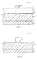
- FIG. 7 is a schematic cross-sectional view of the portion shown in FIG. 1 illustrating the formation of a mask for patterning a diamond layer;
- FIG. 8 is a schematic cross-sectional view of the portion shown in FIG. 1 illustrating the formation of a diamond mask feature
- FIG. 9 is a flow diagram illustrating the process of forming structures in an integrated circuit.
- a portion 10 of an integrated circuit includes a substrate layer 20 , an oxide or dielectric layer 22 , and a line or gate conductor 30 .
- Portion 10 is preferably part of an ultra-large-scale integrated (ULSI) circuit having a million or more transistors, and is manufactured as part of the IC on a wafer made of a semiconducting material (e.g., silicon, gallium arsenide, etc.).
- ULSI ultra-large-scale integrated
- Conductive line 30 can be a metal, a polysilicon, or polysilicon/germanium (Si x Ge (1 ⁇ x) ) material that controls charge carriers in a channel region formed between source and drain regions in substrate 20 to turn the transistor on and off. Conductive line 30 may be doped or undoped. In an exemplary embodiment, conductive line 30 is made of a polysilicon material and has a thickness between approximately 500 and 2000 angstroms and a width of between approximately 30 and 50 nanometers.
- conductive line 30 is preferably formed using a method that maintains the shape integrity of structures formed by reducing or eliminating the phenomenon of warpage or “wiggle.”
- a conductive line formed in an integrated circuit one result is that the tendency to form conductive lines having a generally serpentine or curved shape along their length is reduced or eliminated.
- FIGS. 2A and 2B The warpage phenomenon may be illustrated with reference to FIGS. 2A and 2B.
- FIG. 2A One example of such a conductive line is shown in FIG. 2A, where the sides or lateral edges 32 , 34 of conductive line 30 have a substantially straight or linear configuration along their length.
- FIG. 2B shows a conductive line 40 manufactured by a method that does not reduce or eliminate warpage along the length of conductive line 40 .
- sides or edges 42 , 44 are not linear, but rather include a generally curved or warped shape.
- the amount or magnitude of curvature may vary depending on various conditions, including the properties of the mask or patterning material used, the properties of the material being patterned or etched, and the processing conditions used during the etching operation, among others.
- FIG. 9 is a flow diagram that outlines the process 200 used in the formation of portion 10 .
- a layer 50 of conductive or semiconductive material is provided above or over a layer 22 of dielectric material, which is in turn provided above a silicon wafer 20 .
- Layer 50 may be any of a variety of materials suitable for use in a conductive line or gate structure (e.g., metal, polysilicon, polysilicon/germanium (Si x Ge (1 ⁇ X) ), etc.) and may be doped or undoped.
- Layer 22 may be any of a variety of materials suitable for use as a gate dielectric material (e.g., silicon dioxide, silicon nitride, etc.).
- layer 50 is polysilicon and layer 22 is silicon dioxide thermally grown on silicon substrate 20 .
- layer 50 may include multiple layers of material, one or more of which may include polysilicon.
- layer 50 has a thickness of between approximately 1,500 and 2,000 angstroms and layer 22 has a thickness of between approximately 50 and 200 angstroms. In an alternative embodiment, layer 50 has a thickness of between approximately 1,000 and 2,500 angstroms and layer 22 has a thickness of approximately 10 and 200 angstroms.
- layer 22 can be other types of materials used in the formation of narrow lines or structures.
- Oxide layer 52 When layer 50 is formed, a thin layer 52 of oxide forms on the top or upper surface 54 of polysilicon layer 50 .
- Oxide layer 52 may be referred to as a “native” oxide layer.
- the thickness of oxide layer 52 may vary depending on various processing conditions. In an exemplary embodiment, the thickness of oxide layer 52 is between approximately 50 and 200 angstroms.
- a layer or film 60 of diamond-like material is deposited above or over polysilicon layer 50 .
- Diamond is one of several polymorphic forms of carbon, and is characterized by a diamond cubic crystalline structure in which each carbon atom bonds to four other carbon atoms.
- Layer 60 may have a polycrystalline or single crystalline microstructure. Further, although layer 60 is described as a diamond layer in the disclosure and the claims, it may contain defects and other portions or regions that do not exhibit continuous diamond cubic crystallographic structure. For example, impurities of amorphous carbon and/or graphite forms of carbon may be included in some amounts (e.g., an impurity concentration between approximately 5 and 25 atomic percent). For ease of description, layer 60 may be referred to below simply as a diamond layer.
- Layer 60 is deposited in a plasma-enhanced chemical vapor deposition (PECVD) process using an atmosphere including one or more hydrocarbons such as ethylene, propylene, methane, and the like.
- PECVD plasma-enhanced chemical vapor deposition
- the PECVD process is performed at a temperature of between approximately 250° and 800° C. and a pressure of between approximately 2 and 30 torr with a plasma power of between approximately 100 and 2000 watts. Increasing the temperature, pressure, and/or power increases the diamond-like structure of layer 60 .
- diamond may be deposited in a vapor deposition process at temperatures lower than comparable films (e.g., at temperatures approaching room or ambient temperature).
- the amorphous form of carbon is deposited at elevated temperatures of between approximately 400° and 550° C. In this manner, layer 60 may be deposited without significantly increasing the overall thermal budget of processing.
- the microstructure of the diamond form of carbon provides a film having improved shape integrity, which allows processing of integrated circuits having fewer defects.
- the diamond form of carbon has a relatively high thermal conductivity, which allows the use of a relatively low temperature thermal anneal to relieve internal stresses that may be initially present in the diamond film without adversely increasing the overall thermal budget.
- a diamond material may have an internal stress profile that results in a lesser amount of stress mismatch between the diamond film and adjacent material layers (e.g., adjacent polysilicon or anti-reflective coating materials). As a result, features such as conductive lines may be produced in a manner that reduces or eliminates warpage or wiggle.
- diamond layer 60 has a thickness of between approximately 100 and 1500 angstroms. In alternative embodiments, the thickness of diamond layer 60 may vary depending on various design considerations. For example, the diamond layer may have a thickness of less than 200 angstroms (e.g., between 100 and 200 angstroms or less). In another alternative embodiment, the diamond layer may have a thickness of greater than 1000 angstroms (e.g., between 1000 and 1500 angstroms or greater).
- the diamond layer may be produced in a thickness suitable for patterning polysilicon layer 50 .
- the thickness of the diamond layer may be altered so that the proper amount of mask material is provided over the polysilicon material to compensate for the etch selectivities of the materials used. This allows for increased manufacturing efficiency by eliminating unnecessary material use.
- the diamond layer may be deposited with nitrogen incorporated therein or may be implanted with nitrogen after deposition.
- the diamond layer as deposited may include between approximately 0 and 10 atomic percent nitrogen.
- various other nitrogen concentrations may be achieved by varying the various processing conditions (e.g., increasing or decreasing the gas flow ratio of adjust the level of nitrogen, etc.).
- Cap layer 70 is deposited above or over diamond layer 60 .
- Cap layer 70 may be formed of an anti-reflective material to form an anti-reflective coating (ARC) layer.
- Cap layer 70 may be include silicon nitride (SiN), silicon oxynitride (SiON), silicon-rich oxide (e.g., non-stoichiometric oxide-containing silicon material), silicon-rich nitride, and the like.
- ARC anti-reflective coating
- Cap layer 70 may be include silicon nitride (SiN), silicon oxynitride (SiON), silicon-rich oxide (e.g., non-stoichiometric oxide-containing silicon material), silicon-rich nitride, and the like.
- Cap layer 70 has a thickness of between approximately 200 and 250 angstroms.
- a cap layer formed from an anti-reflective material is that the diamond layer will be protected during deposition and exposure of a photoresist material above diamond layer 60 and that reflection of ultraviolet (UV) rays used in the exposure of the photoresist will be reduced.
- UV ultraviolet
- a layer of photoresist material is deposited above or over cap layer 70 (e.g., by spin-coating) and exposed to form a photoresist feature 80 .
- the layer of photoresist is deposited at a thickness of between approximately 200 and 400 angstroms and is patterned to have a width of between approximately 300 and 800 angstroms. Any of a variety of photoresist materials may be used, including photoresist materials that may be etched using UV rays having wavelengths of 193 or 248 nanometers.
- photoresist feature 80 is trimmed to form a photoresist mask 82 having reduced dimensions. Trimming is accomplished by oxidizing the photoresist feature and removing the oxidized portion, which results in a photoresist mask having reduced dimensions.
- the thickness of the photoresist mask formed may depend on the trim rate. For example, in an exemplary embodiment, a trim etching step may erode or remove between approximately 3 to 4 nanometers per second in the vertical direction and between approximately 1.5 and 2.5 nanometers per second in the lateral direction. Other trim rates may be used, and may depend on the type of photoresist material used. Process 200 is particularly advantageous when narrow gate conductors are formed when using trim etching techniques.
- photoresist mask 82 has a thickness of between approximately 2000 and 8000 angstroms and a width of approximately 30 and 80 nanometers after trim etching.
- photoresist mask 82 is used as a mask to pattern cap layer 70 to form a cap feature 72 .
- a small amount of photoresist material 84 remains through the etching and overetching of cap layer 70 .
- cap layer 70 is etched using a fluorine-based plasma (e.g., CF 4 , CF 4 /CHF 3 , etc.). The etching is performed in an argon or helium atmosphere at a temperature of approximately 20° C. and a pressure of approximately 20 millitorr.
- a diamond mask or mask feature 62 is formed using cap feature 72 as a mask to pattern diamond layer 60 .
- diamond layer 60 is etched using an oxygen-based plasma at a temperature of between approximately ⁇ 10° and 50° C. and a pressure of between approximately 10 and 80 millitorr.
- the plasma used may be an oxygen-hydrogen-bromide plasma, an oxygen-nitrogen plasma, an oxygen-CHF 3 plasma, and the like.
- Argon may also be present in the atmosphere.
- the plasma power may be adjusted so that the ion density power is between approximately 100 and 500 watts and the ion energy control is between approximately 50 and 200 watts.
- diamond mask 62 has a width of between approximately 30 and 60 nanometers.
- diamond mask 62 is formed without the introduction of aqueous etchants, which may damage or destroy mask 62 as processing proceeds.
- aqueous etchants which may damage or destroy mask 62 as processing proceeds.
- the use of phosphoric acid as an etchant is eliminated by using a mask layer of diamond, since portions of the diamond layer may be removed using a plasma etch.
- a breakthrough or native oxide removal etch is performed to remove oxide layer 52 from the surface 54 of polysilicon layer 50 prior to patterning polysilicon layer 50 .
- the breakthrough etch also removes any remaining photoresist and cap material located on top of cap layer 72 .
- the breakthrough etch step is performed using the same conditions as described above with respect to the cap etch (e.g., using a fluorine-based plasma).
- diamond mask 62 is used to pattern or form features in polysilicon layer 50 .
- polysilicon layer 50 may be etched to form conductive line 30 (shown in FIG. 1 ).
- the polysilicon etch is performed using an HBr/CI 2 /HeO 2 /CF 4 mixture at a temperature of between approximately 40 and 70° C. and a pressure of between approximately 3 and 10 millitorr.
- diamond mask 62 is removed after polysilicon layer 50 is patterned (e.g., to form conductive line 30 shown in FIG. 1 ).
- the diamond mask may be removed using a method similar to that described above, in which an oxygen-containing plasma may be used to remove or “ash” away the diamond mask to expose the top surface of conductive line 30 .
- an oxygen-containing plasma may be used to remove or “ash” away the diamond mask to expose the top surface of conductive line 30 .
- other material layers and devices may be added to portion 10 to form a complete integrated circuit.
Abstract
Description
Claims (20)
Priority Applications (1)
| Application Number | Priority Date | Filing Date | Title |
|---|---|---|---|
| US10/335,726 US6673684B1 (en) | 2002-07-31 | 2003-01-02 | Use of diamond as a hard mask material |
Applications Claiming Priority (2)
| Application Number | Priority Date | Filing Date | Title |
|---|---|---|---|
| US39976802P | 2002-07-31 | 2002-07-31 | |
| US10/335,726 US6673684B1 (en) | 2002-07-31 | 2003-01-02 | Use of diamond as a hard mask material |
Publications (1)
| Publication Number | Publication Date |
|---|---|
| US6673684B1 true US6673684B1 (en) | 2004-01-06 |
Family
ID=29739353
Family Applications (1)
| Application Number | Title | Priority Date | Filing Date |
|---|---|---|---|
| US10/335,726 Expired - Lifetime US6673684B1 (en) | 2002-07-31 | 2003-01-02 | Use of diamond as a hard mask material |
Country Status (1)
| Country | Link |
|---|---|
| US (1) | US6673684B1 (en) |
Cited By (65)
| Publication number | Priority date | Publication date | Assignee | Title |
|---|---|---|---|---|
| US20040023502A1 (en) * | 2002-08-02 | 2004-02-05 | Applied Materials Inc. | Undoped and fluorinated amorphous carbon film as pattern mask for metal etch |
| US20040121243A1 (en) * | 2002-12-21 | 2004-06-24 | Manish Chandhok | Damage-resistant coatings for EUV lithography components |
| US6825114B1 (en) * | 2003-04-28 | 2004-11-30 | Advanced Micro Devices, Inc. | Selective stress-inducing implant and resulting pattern distortion in amorphous carbon patterning |
| US6875664B1 (en) | 2002-08-29 | 2005-04-05 | Advanced Micro Devices, Inc. | Formation of amorphous carbon ARC stack having graded transition between amorphous carbon and ARC material |
| US6884733B1 (en) * | 2002-08-08 | 2005-04-26 | Advanced Micro Devices, Inc. | Use of amorphous carbon hard mask for gate patterning to eliminate requirement of poly re-oxidation |
| US20050112506A1 (en) * | 2001-10-29 | 2005-05-26 | Gunter Czech | Photolithographic patterning process using a carbon hard mask layer of diamond-like hardness produced by a plasma-enhanced deposition process |
| US20050277299A1 (en) * | 2004-05-28 | 2005-12-15 | Quang Le | Methods for fabricating read sensor for magnetic heads with reduced read track width |
| US6989332B1 (en) * | 2002-08-13 | 2006-01-24 | Advanced Micro Devices, Inc. | Ion implantation to modulate amorphous carbon stress |
| US20060046422A1 (en) * | 2004-08-31 | 2006-03-02 | Micron Technology, Inc. | Methods for increasing photo alignment margins |
| US20060046201A1 (en) * | 2004-09-02 | 2006-03-02 | Sandhu Gurtej S | Method to align mask patterns |
| US20060046484A1 (en) * | 2004-09-02 | 2006-03-02 | Abatchev Mirzafer K | Method for integrated circuit fabrication using pitch multiplication |
| US20060046200A1 (en) * | 2004-09-01 | 2006-03-02 | Abatchev Mirzafer K | Mask material conversion |
| US7015124B1 (en) | 2003-04-28 | 2006-03-21 | Advanced Micro Devices, Inc. | Use of amorphous carbon for gate patterning |
| US20060145094A1 (en) * | 2004-12-30 | 2006-07-06 | Asml Netherlands B.V. | Optical element, lithographic apparatus including such an optical element, device manufacturing method, and device manufactured thereby |
| US7084071B1 (en) | 2002-09-16 | 2006-08-01 | Advanced Micro Devices, Inc. | Use of multilayer amorphous carbon ARC stack to eliminate line warpage phenomenon |
| US7109101B1 (en) * | 2003-05-06 | 2006-09-19 | Amd, Inc. | Capping layer for reducing amorphous carbon contamination of photoresist in semiconductor device manufacture; and process for making same |
| US20060211260A1 (en) * | 2005-03-15 | 2006-09-21 | Luan Tran | Pitch reduced patterns relative to photolithography features |
| US20060216923A1 (en) * | 2005-03-28 | 2006-09-28 | Tran Luan C | Integrated circuit fabrication |
| US20060231524A1 (en) * | 2004-01-30 | 2006-10-19 | Wei Liu | Techniques for the use of amorphous carbon (apf) for various etch and litho integration schemes |
| US20060263699A1 (en) * | 2005-05-23 | 2006-11-23 | Mirzafer Abatchev | Methods for forming arrays of a small, closely spaced features |
| US20060273456A1 (en) * | 2005-06-02 | 2006-12-07 | Micron Technology, Inc., A Corporation | Multiple spacer steps for pitch multiplication |
| US20060278911A1 (en) * | 2005-06-14 | 2006-12-14 | Eppich Anton P | Relaxed-pitch method of aligning active area to digit line |
| US20060281266A1 (en) * | 2005-06-09 | 2006-12-14 | Wells David H | Method and apparatus for adjusting feature size and position |
| US20070018206A1 (en) * | 2005-07-06 | 2007-01-25 | Leonard Forbes | Surround gate access transistors with grown ultra-thin bodies |
| US20070026672A1 (en) * | 2005-07-29 | 2007-02-01 | Micron Technology, Inc. | Pitch doubled circuit layout |
| US20070045712A1 (en) * | 2005-09-01 | 2007-03-01 | Haller Gordon A | Memory cell layout and process flow |
| US20070049030A1 (en) * | 2005-09-01 | 2007-03-01 | Sandhu Gurtej S | Pitch multiplication spacers and methods of forming the same |
| US20070049040A1 (en) * | 2005-03-15 | 2007-03-01 | Micron Technology, Inc., A Corporation | Multiple deposition for integration of spacers in pitch multiplication process |
| US20070049035A1 (en) * | 2005-08-31 | 2007-03-01 | Tran Luan C | Method of forming pitch multipled contacts |
| US20070049011A1 (en) * | 2005-09-01 | 2007-03-01 | Micron Technology, Inc., A Corporation | Method of forming isolated features using pitch multiplication |
| US20070050748A1 (en) * | 2005-08-30 | 2007-03-01 | Micron Technology, Inc., A Corporation | Method and algorithm for random half pitched interconnect layout with constant spacing |
| US20070051997A1 (en) * | 2005-08-31 | 2007-03-08 | Gordon Haller | Semiconductor memory device |
| US20070090363A1 (en) * | 2005-07-25 | 2007-04-26 | Abbott Todd R | Dram including a vertical surround gate transistor |
| US20070105357A1 (en) * | 2005-09-01 | 2007-05-10 | Micron Technology, Inc. | Silicided recessed silicon |
| US20070205438A1 (en) * | 2006-03-02 | 2007-09-06 | Werner Juengling | Masking process for simultaneously patterning separate regions |
| US20070205443A1 (en) * | 2006-03-02 | 2007-09-06 | Werner Juengling | Vertical gated access transistor |
| US20070238308A1 (en) * | 2006-04-07 | 2007-10-11 | Ardavan Niroomand | Simplified pitch doubling process flow |
| US20070249170A1 (en) * | 2006-04-25 | 2007-10-25 | David Kewley | Process for improving critical dimension uniformity of integrated circuit arrays |
| US20070275332A1 (en) * | 2006-05-25 | 2007-11-29 | Bandic Zvonimir Z | Method for producing high resolution nano-imprinting masters |
| US20070281219A1 (en) * | 2006-06-01 | 2007-12-06 | Sandhu Gurtej S | Masking techniques and contact imprint reticles for dense semiconductor fabrication |
| US20080057724A1 (en) * | 2006-08-31 | 2008-03-06 | Mark Kiehlbauch | Selective etch chemistries for forming high aspect ratio features and associated structures |
| US20080149593A1 (en) * | 2005-08-25 | 2008-06-26 | Micron Technology, Inc. | Multiple deposition for integration of spacers in pitch multiplication process |
| US7393789B2 (en) | 2005-09-01 | 2008-07-01 | Micron Technology, Inc. | Protective coating for planarization |
| US20080299774A1 (en) * | 2007-06-04 | 2008-12-04 | Micron Technology, Inc. | Pitch multiplication using self-assembling materials |
| US20080299753A1 (en) * | 2005-09-01 | 2008-12-04 | Figura Thomas A | Peripheral Gate Stacks and Recessed Array Gates |
| US20090035665A1 (en) * | 2007-07-31 | 2009-02-05 | Micron Technology, Inc. | Process of semiconductor fabrication with mask overlay on pitch multiplied features and associated structures |
| US7521304B1 (en) | 2002-08-29 | 2009-04-21 | Advanced Micro Devices, Inc. | Method for forming integrated circuit |
| US20090152645A1 (en) * | 2007-12-18 | 2009-06-18 | Micron Technology, Inc. | Methods for isolating portions of a loop of pitch-multiplied material and related structures |
| US7572572B2 (en) | 2005-09-01 | 2009-08-11 | Micron Technology, Inc. | Methods for forming arrays of small, closely spaced features |
| US7611980B2 (en) | 2006-08-30 | 2009-11-03 | Micron Technology, Inc. | Single spacer process for multiplying pitch by a factor greater than two and related intermediate IC structures |
| US7659208B2 (en) | 2007-12-06 | 2010-02-09 | Micron Technology, Inc | Method for forming high density patterns |
| US7666578B2 (en) | 2006-09-14 | 2010-02-23 | Micron Technology, Inc. | Efficient pitch multiplication process |
| US20100062579A1 (en) * | 2008-09-11 | 2010-03-11 | Micron Technology, Inc. | Self-aligned trench formation |
| US20100130016A1 (en) * | 2008-11-24 | 2010-05-27 | Micron Technology, Inc. | Methods of forming a masking pattern for integrated circuits |
| US7737039B2 (en) | 2007-11-01 | 2010-06-15 | Micron Technology, Inc. | Spacer process for on pitch contacts and related structures |
| US20100276701A1 (en) * | 2009-04-29 | 2010-11-04 | Hebert Francois | Low thermal resistance and robust chip-scale-package (csp), structure and method |
| US20110121383A1 (en) * | 2005-05-13 | 2011-05-26 | Micron Technology, Inc. | Memory array with surrounding gate access transistors and capacitors with global and staggered local bit lines |
| US20110141696A1 (en) * | 2009-12-15 | 2011-06-16 | Intersil Americas Inc. | Thermal matching in semiconductor devices using heat distribution structures |
| US20110165744A1 (en) * | 2005-05-13 | 2011-07-07 | Micron Technology | Memory array with ultra-thin etched pillar surround gate access transistors and buried data/bit lines |
| US8003310B2 (en) | 2006-04-24 | 2011-08-23 | Micron Technology, Inc. | Masking techniques and templates for dense semiconductor fabrication |
| US8030218B2 (en) | 2008-03-21 | 2011-10-04 | Micron Technology, Inc. | Method for selectively modifying spacing between pitch multiplied structures |
| US8076208B2 (en) | 2008-07-03 | 2011-12-13 | Micron Technology, Inc. | Method for forming transistor with high breakdown voltage using pitch multiplication technique |
| US8114573B2 (en) | 2006-06-02 | 2012-02-14 | Micron Technology, Inc. | Topography based patterning |
| EP2674969A1 (en) * | 2011-02-10 | 2013-12-18 | Think Laboratory Co., Ltd. | Substrate having etching mask and method for producing same |
| US20160064500A1 (en) * | 2014-09-03 | 2016-03-03 | Applied Materials, Inc. | Nanocrystaline diamond carbon film for 3d nand hardmask application |
Citations (7)
| Publication number | Priority date | Publication date | Assignee | Title |
|---|---|---|---|---|
| US5185293A (en) | 1992-04-10 | 1993-02-09 | Eastman Kodak Company | Method of forming and aligning patterns in deposted overlaying on GaAs |
| US5656128A (en) | 1993-03-26 | 1997-08-12 | Fujitsu Limited | Reduction of reflection by amorphous carbon |
| US5759746A (en) | 1996-05-24 | 1998-06-02 | Kabushiki Kaisha Toshiba | Fabrication process using a thin resist |
| US6346747B1 (en) * | 1997-10-14 | 2002-02-12 | International Business Machines Corporation | Method for fabricating a thermally stable diamond-like carbon film as an intralevel or interlevel dielectric in a semiconductor device and device made |
| US6368924B1 (en) | 2000-10-31 | 2002-04-09 | Motorola, Inc. | Amorphous carbon layer for improved adhesion of photoresist and method of fabrication |
| US20020048959A1 (en) * | 2000-06-07 | 2002-04-25 | International Business Machines Corporation | Diamond as a polish-stop layer for chemical-mechanical planarization in a damascene process flow |
| US6388924B1 (en) | 1999-08-02 | 2002-05-14 | Seiko Epson Corporation | Semiconductor integrated device and electronic apparatus mounted with the device |
-
2003
- 2003-01-02 US US10/335,726 patent/US6673684B1/en not_active Expired - Lifetime
Patent Citations (7)
| Publication number | Priority date | Publication date | Assignee | Title |
|---|---|---|---|---|
| US5185293A (en) | 1992-04-10 | 1993-02-09 | Eastman Kodak Company | Method of forming and aligning patterns in deposted overlaying on GaAs |
| US5656128A (en) | 1993-03-26 | 1997-08-12 | Fujitsu Limited | Reduction of reflection by amorphous carbon |
| US5759746A (en) | 1996-05-24 | 1998-06-02 | Kabushiki Kaisha Toshiba | Fabrication process using a thin resist |
| US6346747B1 (en) * | 1997-10-14 | 2002-02-12 | International Business Machines Corporation | Method for fabricating a thermally stable diamond-like carbon film as an intralevel or interlevel dielectric in a semiconductor device and device made |
| US6388924B1 (en) | 1999-08-02 | 2002-05-14 | Seiko Epson Corporation | Semiconductor integrated device and electronic apparatus mounted with the device |
| US20020048959A1 (en) * | 2000-06-07 | 2002-04-25 | International Business Machines Corporation | Diamond as a polish-stop layer for chemical-mechanical planarization in a damascene process flow |
| US6368924B1 (en) | 2000-10-31 | 2002-04-09 | Motorola, Inc. | Amorphous carbon layer for improved adhesion of photoresist and method of fabrication |
Non-Patent Citations (1)
| Title |
|---|
| Sumitomo Derwent Abstracted Publication No. JP 63220524A "Etching diamond semiconductor . . . " Sep. 13, 1988 (abstract only). * |
Cited By (278)
| Publication number | Priority date | Publication date | Assignee | Title |
|---|---|---|---|---|
| US7368390B2 (en) * | 2001-10-29 | 2008-05-06 | Infineon Technologies Ag | Photolithographic patterning process using a carbon hard mask layer of diamond-like hardness produced by a plasma-enhanced deposition process |
| US20050112506A1 (en) * | 2001-10-29 | 2005-05-26 | Gunter Czech | Photolithographic patterning process using a carbon hard mask layer of diamond-like hardness produced by a plasma-enhanced deposition process |
| US6939808B2 (en) * | 2002-08-02 | 2005-09-06 | Applied Materials, Inc. | Undoped and fluorinated amorphous carbon film as pattern mask for metal etch |
| US20040023502A1 (en) * | 2002-08-02 | 2004-02-05 | Applied Materials Inc. | Undoped and fluorinated amorphous carbon film as pattern mask for metal etch |
| US6884733B1 (en) * | 2002-08-08 | 2005-04-26 | Advanced Micro Devices, Inc. | Use of amorphous carbon hard mask for gate patterning to eliminate requirement of poly re-oxidation |
| US6989332B1 (en) * | 2002-08-13 | 2006-01-24 | Advanced Micro Devices, Inc. | Ion implantation to modulate amorphous carbon stress |
| US7521304B1 (en) | 2002-08-29 | 2009-04-21 | Advanced Micro Devices, Inc. | Method for forming integrated circuit |
| US6875664B1 (en) | 2002-08-29 | 2005-04-05 | Advanced Micro Devices, Inc. | Formation of amorphous carbon ARC stack having graded transition between amorphous carbon and ARC material |
| US7084071B1 (en) | 2002-09-16 | 2006-08-01 | Advanced Micro Devices, Inc. | Use of multilayer amorphous carbon ARC stack to eliminate line warpage phenomenon |
| US6982133B2 (en) * | 2002-12-21 | 2006-01-03 | Intel Corporation | Damage-resistant coatings for EUV lithography components |
| US20040121243A1 (en) * | 2002-12-21 | 2004-06-24 | Manish Chandhok | Damage-resistant coatings for EUV lithography components |
| US6825114B1 (en) * | 2003-04-28 | 2004-11-30 | Advanced Micro Devices, Inc. | Selective stress-inducing implant and resulting pattern distortion in amorphous carbon patterning |
| US7015124B1 (en) | 2003-04-28 | 2006-03-21 | Advanced Micro Devices, Inc. | Use of amorphous carbon for gate patterning |
| US7109101B1 (en) * | 2003-05-06 | 2006-09-19 | Amd, Inc. | Capping layer for reducing amorphous carbon contamination of photoresist in semiconductor device manufacture; and process for making same |
| US20060231524A1 (en) * | 2004-01-30 | 2006-10-19 | Wei Liu | Techniques for the use of amorphous carbon (apf) for various etch and litho integration schemes |
| US7718081B2 (en) * | 2004-01-30 | 2010-05-18 | Applied Materials, Inc. | Techniques for the use of amorphous carbon (APF) for various etch and litho integration schemes |
| US20050277299A1 (en) * | 2004-05-28 | 2005-12-15 | Quang Le | Methods for fabricating read sensor for magnetic heads with reduced read track width |
| US7037847B2 (en) | 2004-05-28 | 2006-05-02 | Hitachi Global Storage Technologies Netherlands, B.V. | Methods for fabricating read sensor for magnetic heads with reduced read track width |
| US7361569B2 (en) | 2004-08-31 | 2008-04-22 | Micron Technology, Inc. | Methods for increasing photo-alignment margins |
| US8030222B2 (en) | 2004-08-31 | 2011-10-04 | Round Rock Research, Llc | Structures with increased photo-alignment margins |
| US7368362B2 (en) | 2004-08-31 | 2008-05-06 | Micron Technology, Inc. | Methods for increasing photo alignment margins |
| US20060264001A1 (en) * | 2004-08-31 | 2006-11-23 | Luan Tran | Structures with increased photo-alignment margins |
| US7268054B2 (en) | 2004-08-31 | 2007-09-11 | Micron Technology, Inc. | Methods for increasing photo-alignment margins |
| US7151040B2 (en) | 2004-08-31 | 2006-12-19 | Micron Technology, Inc. | Methods for increasing photo alignment margins |
| US20060228854A1 (en) * | 2004-08-31 | 2006-10-12 | Luan Tran | Methods for increasing photo alignment margins |
| US20060046422A1 (en) * | 2004-08-31 | 2006-03-02 | Micron Technology, Inc. | Methods for increasing photo alignment margins |
| US20060264000A1 (en) * | 2004-08-31 | 2006-11-23 | Luan Tran | Methods for increasing photo-alignment margins |
| WO2006028705A2 (en) * | 2004-09-01 | 2006-03-16 | Micron Technology, Inc. | Mask material conversion |
| WO2006028705A3 (en) * | 2004-09-01 | 2006-04-13 | Micron Technology Inc | Mask material conversion |
| US8486610B2 (en) | 2004-09-01 | 2013-07-16 | Micron Technology, Inc. | Mask material conversion |
| US7910288B2 (en) | 2004-09-01 | 2011-03-22 | Micron Technology, Inc. | Mask material conversion |
| US8895232B2 (en) | 2004-09-01 | 2014-11-25 | Micron Technology, Inc. | Mask material conversion |
| US20060046200A1 (en) * | 2004-09-01 | 2006-03-02 | Abatchev Mirzafer K | Mask material conversion |
| US8216949B2 (en) | 2004-09-02 | 2012-07-10 | Round Rock Research, Llc | Method for integrated circuit fabrication using pitch multiplication |
| US20060262511A1 (en) * | 2004-09-02 | 2006-11-23 | Abatchev Mirzafer K | Method for integrated circuit fabrication using pitch multiplication |
| US7115525B2 (en) | 2004-09-02 | 2006-10-03 | Micron Technology, Inc. | Method for integrated circuit fabrication using pitch multiplication |
| US7455956B2 (en) | 2004-09-02 | 2008-11-25 | Micron Technology, Inc. | Method to align mask patterns |
| US7655387B2 (en) | 2004-09-02 | 2010-02-02 | Micron Technology, Inc. | Method to align mask patterns |
| US7435536B2 (en) | 2004-09-02 | 2008-10-14 | Micron Technology, Inc. | Method to align mask patterns |
| US20070190463A1 (en) * | 2004-09-02 | 2007-08-16 | Micron Technology, Inc. | Method to align mask patterns |
| US20060258162A1 (en) * | 2004-09-02 | 2006-11-16 | Abatchev Mirzafer K | Method for integrated circuit fabrication using pitch multiplication |
| US20100092890A1 (en) * | 2004-09-02 | 2010-04-15 | Micron Technology, Inc. | Method to align mask patterns |
| US8338085B2 (en) | 2004-09-02 | 2012-12-25 | Micron Technology, Inc. | Method to align mask patterns |
| US20060240362A1 (en) * | 2004-09-02 | 2006-10-26 | Sandhu Gurtej S | Method to align mask patterns |
| US7547640B2 (en) | 2004-09-02 | 2009-06-16 | Micron Technology, Inc. | Method for integrated circuit fabrication using pitch multiplication |
| US8674512B2 (en) | 2004-09-02 | 2014-03-18 | Micron Technology, Inc. | Method to align mask patterns |
| US7687408B2 (en) | 2004-09-02 | 2010-03-30 | Micron Technology, Inc. | Method for integrated circuit fabrication using pitch multiplication |
| US20060046484A1 (en) * | 2004-09-02 | 2006-03-02 | Abatchev Mirzafer K | Method for integrated circuit fabrication using pitch multiplication |
| US20100203727A1 (en) * | 2004-09-02 | 2010-08-12 | Micron Technology, Inc. | Method for integrated circuit fabrication using pitch multiplication |
| US7629693B2 (en) | 2004-09-02 | 2009-12-08 | Micron Technology, Inc | Method for integrated circuit fabrication using pitch multiplication |
| US20060046201A1 (en) * | 2004-09-02 | 2006-03-02 | Sandhu Gurtej S | Method to align mask patterns |
| US20070148984A1 (en) * | 2004-09-02 | 2007-06-28 | Micron Technology, Inc. | Method for integrated circuit fabrication using pitch multiplication |
| US7196343B2 (en) * | 2004-12-30 | 2007-03-27 | Asml Netherlands B.V. | Optical element, lithographic apparatus including such an optical element, device manufacturing method, and device manufactured thereby |
| US20060145094A1 (en) * | 2004-12-30 | 2006-07-06 | Asml Netherlands B.V. | Optical element, lithographic apparatus including such an optical element, device manufacturing method, and device manufactured thereby |
| US20070049040A1 (en) * | 2005-03-15 | 2007-03-01 | Micron Technology, Inc., A Corporation | Multiple deposition for integration of spacers in pitch multiplication process |
| US20110117743A1 (en) * | 2005-03-15 | 2011-05-19 | Round Rock Research, Llc | Multiple deposition for integration of spacers in pitch multiplication process |
| US20070161251A1 (en) * | 2005-03-15 | 2007-07-12 | Micron Technology, Inc. | Pitch reduced patterns relative to photolithography features |
| US20070138526A1 (en) * | 2005-03-15 | 2007-06-21 | Micron Technology, Inc. | Pitch reduced patterns relative to photolithography features |
| US7651951B2 (en) | 2005-03-15 | 2010-01-26 | Micron Technology, Inc. | Pitch reduced patterns relative to photolithography features |
| US8207576B2 (en) | 2005-03-15 | 2012-06-26 | Round Rock Research, Llc | Pitch reduced patterns relative to photolithography features |
| US8598632B2 (en) | 2005-03-15 | 2013-12-03 | Round Rock Research Llc | Integrated circuit having pitch reduced patterns relative to photoithography features |
| US20070128856A1 (en) * | 2005-03-15 | 2007-06-07 | Micron Technology, Inc. | Pitch reduced patterns relative to photolithography features |
| US20060211260A1 (en) * | 2005-03-15 | 2006-09-21 | Luan Tran | Pitch reduced patterns relative to photolithography features |
| US8048812B2 (en) | 2005-03-15 | 2011-11-01 | Round Rock Research, Llc | Pitch reduced patterns relative to photolithography features |
| US20100210111A1 (en) * | 2005-03-15 | 2010-08-19 | Round Rock Research, Llc | Pitch reduced patterns relative to photolithography features |
| US8119535B2 (en) | 2005-03-15 | 2012-02-21 | Round Rock Research, Llc | Pitch reduced patterns relative to photolithography features |
| US20100092891A1 (en) * | 2005-03-15 | 2010-04-15 | Micron Technology, Inc. | Pitch reduced patterns relative to photolithography features |
| US7253118B2 (en) | 2005-03-15 | 2007-08-07 | Micron Technology, Inc. | Pitch reduced patterns relative to photolithography features |
| US7390746B2 (en) | 2005-03-15 | 2008-06-24 | Micron Technology, Inc. | Multiple deposition for integration of spacers in pitch multiplication process |
| US7884022B2 (en) | 2005-03-15 | 2011-02-08 | Round Rock Research, Llc | Multiple deposition for integration of spacers in pitch multiplication process |
| US7718540B2 (en) | 2005-03-15 | 2010-05-18 | Round Rock Research, Llc | Pitch reduced patterns relative to photolithography features |
| US9147608B2 (en) | 2005-03-28 | 2015-09-29 | Micron Technology, Inc. | Integrated circuit fabrication |
| US9412594B2 (en) | 2005-03-28 | 2016-08-09 | Micron Technology, Inc. | Integrated circuit fabrication |
| US20080227293A1 (en) * | 2005-03-28 | 2008-09-18 | Micron Technology, Inc. | Integrated circuit fabrication |
| US8859362B2 (en) | 2005-03-28 | 2014-10-14 | Micron Technology, Inc. | Integrated circuit fabrication |
| US7611944B2 (en) | 2005-03-28 | 2009-11-03 | Micron Technology, Inc. | Integrated circuit fabrication |
| US8158476B2 (en) | 2005-03-28 | 2012-04-17 | Micron Technology, Inc. | Integrated circuit fabrication |
| US7776683B2 (en) | 2005-03-28 | 2010-08-17 | Micron Technology, Inc. | Integrated circuit fabrication |
| US20060216923A1 (en) * | 2005-03-28 | 2006-09-28 | Tran Luan C | Integrated circuit fabrication |
| US8507341B2 (en) | 2005-03-28 | 2013-08-13 | Micron Technology, Inc. | Integrated circuit fabrication |
| US7648919B2 (en) | 2005-03-28 | 2010-01-19 | Tran Luan C | Integrated circuit fabrication |
| US8609523B2 (en) | 2005-05-13 | 2013-12-17 | Micron Technology, Inc. | Method of making a memory array with surrounding gate access transistors and capacitors with global staggered local bit lines |
| US8101992B2 (en) | 2005-05-13 | 2012-01-24 | Micron Technology, Inc. | Memory array with surrounding gate access transistors and capacitors with global and staggered local bit lines |
| US8227305B2 (en) | 2005-05-13 | 2012-07-24 | Micron Technology, Inc. | Memory array with ultra-thin etched pillar surround gate access transistors and buried data/bit lines |
| US20110121383A1 (en) * | 2005-05-13 | 2011-05-26 | Micron Technology, Inc. | Memory array with surrounding gate access transistors and capacitors with global and staggered local bit lines |
| US8637362B2 (en) | 2005-05-13 | 2014-01-28 | Micron Technology, Inc. | Memory array with ultra-thin etched pillar surround gate access transistors and buried data/bit lines |
| US20110165744A1 (en) * | 2005-05-13 | 2011-07-07 | Micron Technology | Memory array with ultra-thin etched pillar surround gate access transistors and buried data/bit lines |
| US8350320B2 (en) | 2005-05-13 | 2013-01-08 | Micron Technology, Inc. | Memory array and memory device |
| US9099402B2 (en) | 2005-05-23 | 2015-08-04 | Micron Technology, Inc. | Integrated circuit structure having arrays of small, closely spaced features |
| US7429536B2 (en) | 2005-05-23 | 2008-09-30 | Micron Technology, Inc. | Methods for forming arrays of small, closely spaced features |
| US20060263699A1 (en) * | 2005-05-23 | 2006-11-23 | Mirzafer Abatchev | Methods for forming arrays of a small, closely spaced features |
| US8207614B2 (en) | 2005-05-23 | 2012-06-26 | Micron Technology, Inc. | Methods for forming arrays of small, closely spaced features |
| US9117766B2 (en) | 2005-06-02 | 2015-08-25 | Micron Technology, Inc. | Method for positioning spacers in pitch multiplication |
| US8598041B2 (en) | 2005-06-02 | 2013-12-03 | Micron Technology, Inc. | Method for positioning spacers in pitch multiplication |
| US20060273456A1 (en) * | 2005-06-02 | 2006-12-07 | Micron Technology, Inc., A Corporation | Multiple spacer steps for pitch multiplication |
| US7560390B2 (en) | 2005-06-02 | 2009-07-14 | Micron Technology, Inc. | Multiple spacer steps for pitch multiplication |
| US8173550B2 (en) | 2005-06-02 | 2012-05-08 | Micron Technology, Inc. | Method for positioning spacers for pitch multiplication |
| US20090258492A1 (en) * | 2005-06-02 | 2009-10-15 | Micron Technology, Inc. | Multiple spacer steps for pitch multiplication |
| US8003542B2 (en) | 2005-06-02 | 2011-08-23 | Micron Technology, Inc. | Multiple spacer steps for pitch multiplication |
| US8865598B2 (en) | 2005-06-02 | 2014-10-21 | Micron Technology, Inc. | Method for positioning spacers in pitch multiplication |
| US20060281266A1 (en) * | 2005-06-09 | 2006-12-14 | Wells David H | Method and apparatus for adjusting feature size and position |
| US20080254627A1 (en) * | 2005-06-09 | 2008-10-16 | Micron Technology, Inc. | Method for adjusting feature size and position |
| US8703616B2 (en) | 2005-06-09 | 2014-04-22 | Round Rock Research, Llc | Method for adjusting feature size and position |
| US7396781B2 (en) | 2005-06-09 | 2008-07-08 | Micron Technology, Inc. | Method and apparatus for adjusting feature size and position |
| US8354317B2 (en) | 2005-06-14 | 2013-01-15 | Micron Technology, Inc. | Relaxed-pitch method of aligning active area to digit line |
| US20060278911A1 (en) * | 2005-06-14 | 2006-12-14 | Eppich Anton P | Relaxed-pitch method of aligning active area to digit line |
| US20110156116A1 (en) * | 2005-06-14 | 2011-06-30 | Micron Technology, Inc. | Relaxed-pitch method of aligning active area to digit line |
| US7541632B2 (en) | 2005-06-14 | 2009-06-02 | Micron Technology, Inc. | Relaxed-pitch method of aligning active area to digit line |
| US20090215236A1 (en) * | 2005-06-14 | 2009-08-27 | Micron Technology, Inc. | Relaxed-pitch method of aligning active area to digit line |
| US7915116B2 (en) | 2005-06-14 | 2011-03-29 | Micron Technology, Inc. | Relaxed-pitch method of aligning active area to digit line |
| US7888721B2 (en) | 2005-07-06 | 2011-02-15 | Micron Technology, Inc. | Surround gate access transistors with grown ultra-thin bodies |
| US20070114576A1 (en) * | 2005-07-06 | 2007-05-24 | Leonard Forbes | Surround gate access transistors with grown ultra-thin bodies |
| US20070018206A1 (en) * | 2005-07-06 | 2007-01-25 | Leonard Forbes | Surround gate access transistors with grown ultra-thin bodies |
| US20110140184A1 (en) * | 2005-07-06 | 2011-06-16 | Leonard Forbes | Surround gate access transistors with grown ultra-thin bodies |
| US8115243B2 (en) | 2005-07-06 | 2012-02-14 | Micron Technology, Inc. | Surround gate access transistors with grown ultra-thin bodies |
| US20070090363A1 (en) * | 2005-07-25 | 2007-04-26 | Abbott Todd R | Dram including a vertical surround gate transistor |
| US7768051B2 (en) | 2005-07-25 | 2010-08-03 | Micron Technology, Inc. | DRAM including a vertical surround gate transistor |
| US8264010B2 (en) | 2005-07-29 | 2012-09-11 | Round Rock Research, Llc | Layout for high density conductive interconnects |
| US20070026672A1 (en) * | 2005-07-29 | 2007-02-01 | Micron Technology, Inc. | Pitch doubled circuit layout |
| US7767573B2 (en) | 2005-07-29 | 2010-08-03 | Round Rock Research, Llc | Layout for high density conductive interconnects |
| US20110006347A1 (en) * | 2005-07-29 | 2011-01-13 | Round Rock Research, Llc | Layout for high density conductive interconnects |
| US20080290374A1 (en) * | 2005-07-29 | 2008-11-27 | Micron Technology, Inc. | Layout for high density conductive interconnects |
| US7413981B2 (en) | 2005-07-29 | 2008-08-19 | Micron Technology, Inc. | Pitch doubled circuit layout |
| US20080149593A1 (en) * | 2005-08-25 | 2008-06-26 | Micron Technology, Inc. | Multiple deposition for integration of spacers in pitch multiplication process |
| US8123968B2 (en) | 2005-08-25 | 2012-02-28 | Round Rock Research, Llc | Multiple deposition for integration of spacers in pitch multiplication process |
| US8148247B2 (en) | 2005-08-30 | 2012-04-03 | Micron Technology, Inc. | Method and algorithm for random half pitched interconnect layout with constant spacing |
| US20110034024A1 (en) * | 2005-08-30 | 2011-02-10 | Micron Technology, Inc. | Method and algorithm for random half pitched interconnect layout with constant spacing |
| US20070050748A1 (en) * | 2005-08-30 | 2007-03-01 | Micron Technology, Inc., A Corporation | Method and algorithm for random half pitched interconnect layout with constant spacing |
| US7816262B2 (en) | 2005-08-30 | 2010-10-19 | Micron Technology, Inc. | Method and algorithm for random half pitched interconnect layout with constant spacing |
| US8877639B2 (en) | 2005-08-30 | 2014-11-04 | Micron Technology, Inc. | Method and algorithm for random half pitched interconnect layout with constant spacing |
| US8546215B2 (en) | 2005-08-31 | 2013-10-01 | Micron Technology, Inc. | Methods of fabricating a memory device |
| US20100144107A1 (en) * | 2005-08-31 | 2010-06-10 | Micron Technology, Inc. | Semiconductor Memory Device |
| US8609324B2 (en) | 2005-08-31 | 2013-12-17 | Micron Technology, Inc. | Method of forming pitch multiplied contacts |
| US20070051997A1 (en) * | 2005-08-31 | 2007-03-08 | Gordon Haller | Semiconductor memory device |
| US20110014574A1 (en) * | 2005-08-31 | 2011-01-20 | Micron Technology, Inc. | Method of forming pitch multipled contacts |
| US8481385B2 (en) | 2005-08-31 | 2013-07-09 | Micron Technology, Inc. | Methods of fabricating a memory device |
| US8222105B2 (en) | 2005-08-31 | 2012-07-17 | Micron Technology, Inc. | Methods of fabricating a memory device |
| US7696567B2 (en) | 2005-08-31 | 2010-04-13 | Micron Technology, Inc | Semiconductor memory device |
| US7829262B2 (en) | 2005-08-31 | 2010-11-09 | Micron Technology, Inc. | Method of forming pitch multipled contacts |
| US8426118B2 (en) | 2005-08-31 | 2013-04-23 | Micron Technology, Inc. | Method of forming pitch multiplied contacts |
| US20070049035A1 (en) * | 2005-08-31 | 2007-03-01 | Tran Luan C | Method of forming pitch multipled contacts |
| US8601410B2 (en) | 2005-09-01 | 2013-12-03 | Micron Technology, Inc. | Methods for forming arrays of small, closely spaced features |
| US8043915B2 (en) | 2005-09-01 | 2011-10-25 | Micron Technology, Inc. | Pitch multiplied mask patterns for isolated features |
| US20080261349A1 (en) * | 2005-09-01 | 2008-10-23 | Micron Technology, Inc. | Protective coating for planarization |
| US20070049030A1 (en) * | 2005-09-01 | 2007-03-01 | Sandhu Gurtej S | Pitch multiplication spacers and methods of forming the same |
| US9099314B2 (en) | 2005-09-01 | 2015-08-04 | Micron Technology, Inc. | Pitch multiplication spacers and methods of forming the same |
| US7393789B2 (en) | 2005-09-01 | 2008-07-01 | Micron Technology, Inc. | Protective coating for planarization |
| US20100148249A1 (en) * | 2005-09-01 | 2010-06-17 | Micron Technology, Inc. | Method Of Manufacturing A Memory Device |
| US8266558B2 (en) | 2005-09-01 | 2012-09-11 | Micron Technology, Inc. | Methods for forming arrays of small, closely spaced features |
| US7687342B2 (en) | 2005-09-01 | 2010-03-30 | Micron Technology, Inc. | Method of manufacturing a memory device |
| US20070049011A1 (en) * | 2005-09-01 | 2007-03-01 | Micron Technology, Inc., A Corporation | Method of forming isolated features using pitch multiplication |
| US7935999B2 (en) | 2005-09-01 | 2011-05-03 | Micron Technology, Inc. | Memory device |
| US7939409B2 (en) | 2005-09-01 | 2011-05-10 | Micron Technology, Inc. | Peripheral gate stacks and recessed array gates |
| US9082829B2 (en) | 2005-09-01 | 2015-07-14 | Micron Technology, Inc. | Methods for forming arrays of small, closely spaced features |
| US9076888B2 (en) | 2005-09-01 | 2015-07-07 | Micron Technology, Inc. | Silicided recessed silicon |
| US9003651B2 (en) | 2005-09-01 | 2015-04-14 | Micron Technology, Inc. | Methods for integrated circuit fabrication with protective coating for planarization |
| US20100267240A1 (en) * | 2005-09-01 | 2010-10-21 | Micron Technology, Inc. | Pitch multiplication spacers and methods of forming the same |
| US8252646B2 (en) | 2005-09-01 | 2012-08-28 | Micron Technology, Inc. | Peripheral gate stacks and recessed array gates |
| US20100243161A1 (en) * | 2005-09-01 | 2010-09-30 | Micron Technology, Inc. | Pitch multiplied mask patterns for isolated features |
| US7977236B2 (en) | 2005-09-01 | 2011-07-12 | Micron Technology, Inc. | Method of forming a transistor gate of a recessed access device, method of forming a recessed transistor gate and a non-recessed transistor gate, and method of fabricating an integrated circuit |
| US20110183507A1 (en) * | 2005-09-01 | 2011-07-28 | Micron Technology Inc. | Peripheral Gate Stacks and Recessed Array Gates |
| US20090271758A1 (en) * | 2005-09-01 | 2009-10-29 | Micron Technology, Inc. | Methods for forming arrays of small, closely spaced features |
| US7759197B2 (en) | 2005-09-01 | 2010-07-20 | Micron Technology, Inc. | Method of forming isolated features using pitch multiplication |
| US20070105357A1 (en) * | 2005-09-01 | 2007-05-10 | Micron Technology, Inc. | Silicided recessed silicon |
| US8011090B2 (en) | 2005-09-01 | 2011-09-06 | Micron Technology, Inc. | Method for forming and planarizing adjacent regions of an integrated circuit |
| US20080299753A1 (en) * | 2005-09-01 | 2008-12-04 | Figura Thomas A | Peripheral Gate Stacks and Recessed Array Gates |
| US10396281B2 (en) | 2005-09-01 | 2019-08-27 | Micron Technology, Inc. | Methods for forming arrays of small, closely spaced features |
| US20090239366A1 (en) * | 2005-09-01 | 2009-09-24 | Hasan Nejad | Method Of Forming A Transistor Gate Of A Recessed Access Device, Method Of Forming A Recessed Transistor Gate And A Non-Recessed Transistor Gate, And Method Of Fabricating An Integrated Circuit |
| US8431971B2 (en) | 2005-09-01 | 2013-04-30 | Micron Technology, Inc. | Pitch multiplied mask patterns for isolated features |
| US8479384B2 (en) | 2005-09-01 | 2013-07-09 | Micron Technology, Inc. | Methods for integrated circuit fabrication with protective coating for planarization |
| US7572572B2 (en) | 2005-09-01 | 2009-08-11 | Micron Technology, Inc. | Methods for forming arrays of small, closely spaced features |
| US7776744B2 (en) | 2005-09-01 | 2010-08-17 | Micron Technology, Inc. | Pitch multiplication spacers and methods of forming the same |
| US9679781B2 (en) | 2005-09-01 | 2017-06-13 | Micron Technology, Inc. | Methods for integrated circuit fabrication with protective coating for planarization |
| US20070045712A1 (en) * | 2005-09-01 | 2007-03-01 | Haller Gordon A | Memory cell layout and process flow |
| US9184161B2 (en) | 2006-03-02 | 2015-11-10 | Micron Technology, Inc. | Vertical gated access transistor |
| US8772840B2 (en) | 2006-03-02 | 2014-07-08 | Micron Technology, Inc. | Memory device comprising an array portion and a logic portion |
| US7736980B2 (en) | 2006-03-02 | 2010-06-15 | Micron Technology, Inc. | Vertical gated access transistor |
| US8592898B2 (en) | 2006-03-02 | 2013-11-26 | Micron Technology, Inc. | Vertical gated access transistor |
| US20110042755A1 (en) * | 2006-03-02 | 2011-02-24 | Micron Technology, Inc. | Memory device comprising an array portion and a logic portion |
| US20070205443A1 (en) * | 2006-03-02 | 2007-09-06 | Werner Juengling | Vertical gated access transistor |
| US20090104744A1 (en) * | 2006-03-02 | 2009-04-23 | Micron Technology, Inc. | Vertical gated access transistor |
| US8207583B2 (en) | 2006-03-02 | 2012-06-26 | Micron Technology, Inc. | Memory device comprising an array portion and a logic portion |
| US7842558B2 (en) | 2006-03-02 | 2010-11-30 | Micron Technology, Inc. | Masking process for simultaneously patterning separate regions |
| US20100230733A1 (en) * | 2006-03-02 | 2010-09-16 | Micron Technology, Inc. | Vertical gated access transistor |
| US20070205438A1 (en) * | 2006-03-02 | 2007-09-06 | Werner Juengling | Masking process for simultaneously patterning separate regions |
| US8039348B2 (en) | 2006-03-02 | 2011-10-18 | Micron Technology, Inc. | Vertical gated access transistor |
| US7476933B2 (en) | 2006-03-02 | 2009-01-13 | Micron Technology, Inc. | Vertical gated access transistor |
| US7902074B2 (en) | 2006-04-07 | 2011-03-08 | Micron Technology, Inc. | Simplified pitch doubling process flow |
| US8030217B2 (en) | 2006-04-07 | 2011-10-04 | Micron Technology, Inc. | Simplified pitch doubling process flow |
| US20070238299A1 (en) * | 2006-04-07 | 2007-10-11 | Micron Technology, Inc. | Simplified pitch doubling process flow |
| US9184159B2 (en) | 2006-04-07 | 2015-11-10 | Micron Technology, Inc. | Simplified pitch doubling process flow |
| US7732343B2 (en) | 2006-04-07 | 2010-06-08 | Micron Technology, Inc. | Simplified pitch doubling process flow |
| US20070238308A1 (en) * | 2006-04-07 | 2007-10-11 | Ardavan Niroomand | Simplified pitch doubling process flow |
| US8338959B2 (en) | 2006-04-07 | 2012-12-25 | Micron Technology, Inc. | Simplified pitch doubling process flow |
| US8003310B2 (en) | 2006-04-24 | 2011-08-23 | Micron Technology, Inc. | Masking techniques and templates for dense semiconductor fabrication |
| US8334211B2 (en) | 2006-04-25 | 2012-12-18 | Micron Technology, Inc. | Process for improving critical dimension uniformity of integrated circuit arrays |
| US9553082B2 (en) | 2006-04-25 | 2017-01-24 | Micron Technology, Inc. | Process for improving critical dimension uniformity of integrated circuit arrays |
| US20070249170A1 (en) * | 2006-04-25 | 2007-10-25 | David Kewley | Process for improving critical dimension uniformity of integrated circuit arrays |
| US20090130852A1 (en) * | 2006-04-25 | 2009-05-21 | Micron Technology, Inc. | Process for improving critical dimension uniformity of integrated circuit arrays |
| US7488685B2 (en) | 2006-04-25 | 2009-02-10 | Micron Technology, Inc. | Process for improving critical dimension uniformity of integrated circuit arrays |
| US8889020B2 (en) | 2006-04-25 | 2014-11-18 | Micron Technology, Inc. | Process for improving critical dimension uniformity of integrated circuit arrays |
| US7341825B2 (en) | 2006-05-25 | 2008-03-11 | Hitachi Global Storage Technologies Netherlands B.V. | Method for producing high resolution nano-imprinting masters |
| US20070275332A1 (en) * | 2006-05-25 | 2007-11-29 | Bandic Zvonimir Z | Method for producing high resolution nano-imprinting masters |
| US8663532B2 (en) | 2006-06-01 | 2014-03-04 | Micron Technology, Inc. | Masking techniques and contact imprint reticles for dense semiconductor fabrication |
| US8449805B2 (en) | 2006-06-01 | 2013-05-28 | Micron Technology, Inc. | Masking techniques and contact imprint reticles for dense semiconductor fabrication |
| US20100258966A1 (en) * | 2006-06-01 | 2010-10-14 | Micron Technology, Inc. | Masking techniques and contact imprint reticles for dense semiconductor fabrication |
| US7795149B2 (en) | 2006-06-01 | 2010-09-14 | Micron Technology, Inc. | Masking techniques and contact imprint reticles for dense semiconductor fabrication |
| US20070281219A1 (en) * | 2006-06-01 | 2007-12-06 | Sandhu Gurtej S | Masking techniques and contact imprint reticles for dense semiconductor fabrication |
| US8114573B2 (en) | 2006-06-02 | 2012-02-14 | Micron Technology, Inc. | Topography based patterning |
| US8592940B2 (en) | 2006-06-02 | 2013-11-26 | Micron Technology, Inc. | Topography based patterning |
| US8883644B2 (en) | 2006-08-30 | 2014-11-11 | Micron Technology, Inc. | Single spacer process for multiplying pitch by a factor greater than two and related intermediate IC structures |
| US8557704B2 (en) | 2006-08-30 | 2013-10-15 | Micron Technology, Inc. | Single spacer process for multiplying pitch by a factor greater than two and related intermediate IC structures |
| US7611980B2 (en) | 2006-08-30 | 2009-11-03 | Micron Technology, Inc. | Single spacer process for multiplying pitch by a factor greater than two and related intermediate IC structures |
| US9478497B2 (en) | 2006-08-30 | 2016-10-25 | Micron Technology, Inc. | Single spacer process for multiplying pitch by a factor greater than two and related intermediate IC structures |
| US20100029081A1 (en) * | 2006-08-30 | 2010-02-04 | Micron Technology, Inc. | Single spacer process for multiplying pitch by a factor greater than two and related intermediate ic structures |
| US20090159560A1 (en) * | 2006-08-31 | 2009-06-25 | Micron Technology, Inc. | Selective etch chemistries for forming high aspect ratio features and associated structures |
| US7517804B2 (en) | 2006-08-31 | 2009-04-14 | Micron Technologies, Inc. | Selective etch chemistries for forming high aspect ratio features and associated structures |
| US8088691B2 (en) | 2006-08-31 | 2012-01-03 | Micron Technology, Inc. | Selective etch chemistries for forming high aspect ratio features and associated structures |
| US20080057724A1 (en) * | 2006-08-31 | 2008-03-06 | Mark Kiehlbauch | Selective etch chemistries for forming high aspect ratio features and associated structures |
| US20100112489A1 (en) * | 2006-09-14 | 2010-05-06 | Micron Technology, Inc. | Efficient pitch multiplication process |
| US8012674B2 (en) | 2006-09-14 | 2011-09-06 | Micron Technology, Inc. | Efficient pitch multiplication process |
| US9035416B2 (en) | 2006-09-14 | 2015-05-19 | Micron Technology, Inc. | Efficient pitch multiplication process |
| US8450829B2 (en) | 2006-09-14 | 2013-05-28 | Micron Technology, Inc. | Efficient pitch multiplication process |
| US7666578B2 (en) | 2006-09-14 | 2010-02-23 | Micron Technology, Inc. | Efficient pitch multiplication process |
| US20080299774A1 (en) * | 2007-06-04 | 2008-12-04 | Micron Technology, Inc. | Pitch multiplication using self-assembling materials |
| US7923373B2 (en) | 2007-06-04 | 2011-04-12 | Micron Technology, Inc. | Pitch multiplication using self-assembling materials |
| US10515801B2 (en) | 2007-06-04 | 2019-12-24 | Micron Technology, Inc. | Pitch multiplication using self-assembling materials |
| US20090035665A1 (en) * | 2007-07-31 | 2009-02-05 | Micron Technology, Inc. | Process of semiconductor fabrication with mask overlay on pitch multiplied features and associated structures |
| US9412591B2 (en) | 2007-07-31 | 2016-08-09 | Micron Technology, Inc. | Process of semiconductor fabrication with mask overlay on pitch multiplied features and associated structures |
| US8563229B2 (en) | 2007-07-31 | 2013-10-22 | Micron Technology, Inc. | Process of semiconductor fabrication with mask overlay on pitch multiplied features and associated structures |
| US8211803B2 (en) | 2007-11-01 | 2012-07-03 | Micron Technology, Inc. | Spacer process for on pitch contacts and related structures |
| US8772166B2 (en) | 2007-11-01 | 2014-07-08 | Micron Technology, Inc. | Spacer process for on pitch contacts and related structures |
| US7737039B2 (en) | 2007-11-01 | 2010-06-15 | Micron Technology, Inc. | Spacer process for on pitch contacts and related structures |
| US7659208B2 (en) | 2007-12-06 | 2010-02-09 | Micron Technology, Inc | Method for forming high density patterns |
| US8324107B2 (en) | 2007-12-06 | 2012-12-04 | Micron Technology, Inc. | Method for forming high density patterns |
| US8871648B2 (en) | 2007-12-06 | 2014-10-28 | Micron Technology, Inc. | Method for forming high density patterns |
| US8932960B2 (en) | 2007-12-18 | 2015-01-13 | Micron Technology, Inc. | Methods for isolating portions of a loop of pitch-multiplied material and related structures |
| US9666695B2 (en) | 2007-12-18 | 2017-05-30 | Micron Technology, Inc. | Methods for isolating portions of a loop of pitch-multiplied material and related structures |
| US7790531B2 (en) | 2007-12-18 | 2010-09-07 | Micron Technology, Inc. | Methods for isolating portions of a loop of pitch-multiplied material and related structures |
| US9941155B2 (en) | 2007-12-18 | 2018-04-10 | Micron Technology, Inc. | Methods for isolating portions of a loop of pitch-multiplied material and related structures |
| US8390034B2 (en) | 2007-12-18 | 2013-03-05 | Micron Technology, Inc. | Methods for isolating portions of a loop of pitch-multiplied material and related structures |
| US10497611B2 (en) | 2007-12-18 | 2019-12-03 | Micron Technology, Inc. | Methods for isolating portions of a loop of pitch-multiplied material and related structures |
| US20090152645A1 (en) * | 2007-12-18 | 2009-06-18 | Micron Technology, Inc. | Methods for isolating portions of a loop of pitch-multiplied material and related structures |
| US20100289070A1 (en) * | 2007-12-18 | 2010-11-18 | Micron Technology, Inc. | Methods for isolating portions of a loop of pitch-multiplied material and related structures |
| US8030218B2 (en) | 2008-03-21 | 2011-10-04 | Micron Technology, Inc. | Method for selectively modifying spacing between pitch multiplied structures |
| US9048194B2 (en) | 2008-03-21 | 2015-06-02 | Micron Technology, Inc. | Method for selectively modifying spacing between pitch multiplied structures |
| US8507384B2 (en) | 2008-03-21 | 2013-08-13 | Micron Technology, Inc. | Method for selectively modifying spacing between pitch multiplied structures |
| US8076208B2 (en) | 2008-07-03 | 2011-12-13 | Micron Technology, Inc. | Method for forming transistor with high breakdown voltage using pitch multiplication technique |
| US8928111B2 (en) | 2008-07-03 | 2015-01-06 | Micron Technology, Inc. | Transistor with high breakdown voltage having separated drain extensions |
| US8343875B2 (en) | 2008-09-11 | 2013-01-01 | Micron Technology, Inc. | Methods of forming an integrated circuit with self-aligned trench formation |
| US20100062579A1 (en) * | 2008-09-11 | 2010-03-11 | Micron Technology, Inc. | Self-aligned trench formation |
| US8101497B2 (en) | 2008-09-11 | 2012-01-24 | Micron Technology, Inc. | Self-aligned trench formation |
| US8685859B2 (en) | 2008-09-11 | 2014-04-01 | Micron Technology, Inc. | Self-aligned semiconductor trench structures |
| US8552526B2 (en) | 2008-09-11 | 2013-10-08 | Micron Technology, Inc. | Self-aligned semiconductor trench structures |
| US8492282B2 (en) | 2008-11-24 | 2013-07-23 | Micron Technology, Inc. | Methods of forming a masking pattern for integrated circuits |
| US20100130016A1 (en) * | 2008-11-24 | 2010-05-27 | Micron Technology, Inc. | Methods of forming a masking pattern for integrated circuits |
| US8871646B2 (en) | 2008-11-24 | 2014-10-28 | Micron Technology, Inc. | Methods of forming a masking pattern for integrated circuits |
| US20100276701A1 (en) * | 2009-04-29 | 2010-11-04 | Hebert Francois | Low thermal resistance and robust chip-scale-package (csp), structure and method |
| US20110141696A1 (en) * | 2009-12-15 | 2011-06-16 | Intersil Americas Inc. | Thermal matching in semiconductor devices using heat distribution structures |
| US8859337B2 (en) | 2009-12-15 | 2014-10-14 | Soitec | Thermal matching in semiconductor devices using heat distribution structures |
| US20130337231A1 (en) * | 2011-02-10 | 2013-12-19 | Think Laboratory Co., Ltd. | Substrate having etching mask and method for producing same |
| EP2674969A1 (en) * | 2011-02-10 | 2013-12-18 | Think Laboratory Co., Ltd. | Substrate having etching mask and method for producing same |
| EP2674969A4 (en) * | 2011-02-10 | 2017-04-26 | Think Laboratory Co., Ltd. | Substrate having etching mask and method for producing same |
| RU2562923C2 (en) * | 2011-02-10 | 2015-09-10 | Тинк Лаборатори Ко., Лтд. | Production of substrate with etching mask and making of article with pattern |
| US9188873B2 (en) * | 2011-02-10 | 2015-11-17 | Think Laboratory Co., Ltd. | Substrate having etching mask and method for producing same |
| WO2016036533A1 (en) * | 2014-09-03 | 2016-03-10 | Applied Materials, Inc. | Nanocrystalline diamond carbon film for 3d nand hardmask application |
| KR20170081716A (en) * | 2014-09-03 | 2017-07-12 | 어플라이드 머티어리얼스, 인코포레이티드 | Nanocrystalline diamond carbon film for 3d nand hardmask application |
| JP2017533580A (en) * | 2014-09-03 | 2017-11-09 | アプライド マテリアルズ インコーポレイテッドApplied Materials,Incorporated | Nanocrystalline diamond carbon film for 3D NAND hard mask applications |
| US9865464B2 (en) * | 2014-09-03 | 2018-01-09 | Applied Materials, Inc. | Nanocrystalline diamond carbon film for 3D NAND hardmask application |
| US20160064500A1 (en) * | 2014-09-03 | 2016-03-03 | Applied Materials, Inc. | Nanocrystaline diamond carbon film for 3d nand hardmask application |
| TWI656575B (en) * | 2014-09-03 | 2019-04-11 | 美商應用材料股份有限公司 | Nanocrystalline diamond carbon film for 3D NAND hard mask applications |
| US20170062216A1 (en) * | 2014-09-03 | 2017-03-02 | Applied Materials, Inc. | Nanocrystaline diamond carbon film for 3d nand hardmask application |
| TWI670831B (en) * | 2014-09-03 | 2019-09-01 | 美商應用材料股份有限公司 | Nanocrystalline diamond carbon film for 3d nand hardmask application |
| CN106796883A (en) * | 2014-09-03 | 2017-05-31 | 应用材料公司 | For the nanocrystalline diamond carbon film of three dimensional NAND dura mater application |
| US9502262B2 (en) * | 2014-09-03 | 2016-11-22 | Applied Materials, Inc. | Nanocrystalline diamond carbon film for 3D NAND hardmask application |
| CN106796883B (en) * | 2014-09-03 | 2020-08-28 | 应用材料公司 | Nanocrystalline diamond carbon films for three-dimensional NAND hard film applications |
| CN112053950A (en) * | 2014-09-03 | 2020-12-08 | 应用材料公司 | Nanocrystalline diamond carbon films for three-dimensional NAND hard film applications |
| KR102250012B1 (en) | 2014-09-03 | 2021-05-07 | 어플라이드 머티어리얼스, 인코포레이티드 | Nanocrystalline diamond carbon film for 3d nand hardmask application |
Similar Documents
| Publication | Publication Date | Title |
|---|---|---|
| US6673684B1 (en) | Use of diamond as a hard mask material | |
| US6773998B1 (en) | Modified film stack and patterning strategy for stress compensation and prevention of pattern distortion in amorphous carbon gate patterning | |
| US6884733B1 (en) | Use of amorphous carbon hard mask for gate patterning to eliminate requirement of poly re-oxidation | |
| US7015124B1 (en) | Use of amorphous carbon for gate patterning | |
| US6875664B1 (en) | Formation of amorphous carbon ARC stack having graded transition between amorphous carbon and ARC material | |
| KR100957820B1 (en) | Manufacturing method of fin-type field effect transistor | |
| US6716761B2 (en) | Method of forming fine patterns | |
| US7084071B1 (en) | Use of multilayer amorphous carbon ARC stack to eliminate line warpage phenomenon | |
| US8222100B2 (en) | CMOS circuit with low-k spacer and stress liner | |
| US6555472B2 (en) | Method of producing a semiconductor device using feature trimming | |
| US8629535B2 (en) | Mask for forming integrated circuit | |
| US6100160A (en) | Oxide etch barrier formed by nitridation | |
| JP2009515360A (en) | Electronic device including a transistor structure having an active region adjacent to a stressor layer and method of manufacturing the electronic device | |
| US6541320B2 (en) | Method to controllably form notched polysilicon gate structures | |
| US6989332B1 (en) | Ion implantation to modulate amorphous carbon stress | |
| US6586293B1 (en) | Semiconductor device and method of manufacturing the same | |
| US6509219B2 (en) | Fabrication of notched gates by passivating partially etched gate sidewalls and then using an isotropic etch | |
| US6927135B2 (en) | Methods of fabricating multiple sets of field effect transistors | |
| KR100446302B1 (en) | Semiconductor device having gate with negative slope and fabricating method the same | |
| JP2004134719A (en) | Manufacturing method for semiconductor element | |
| US6423648B2 (en) | Controllable oxidation technique for the formation of high-quality ultra-thin gate oxide using carbon dioxide as the oxidizing agent | |
| US6849508B2 (en) | Method of forming multiple gate insulators on a strained semiconductor heterostructure | |
| US8169032B2 (en) | Gate stacks and semiconductor constructions | |
| US6211054B1 (en) | Method of forming a conductive line and method of forming a local interconnect | |
| US7169714B2 (en) | Method and structure for graded gate oxides on vertical and non-planar surfaces |
Legal Events
| Date | Code | Title | Description |
|---|---|---|---|
| AS | Assignment |
Owner name: ADVANCED MICRO DEVICES, INC., CALIFORNIA Free format text: ASSIGNMENT OF ASSIGNORS INTEREST;ASSIGNORS:HUANG, RICHARD J.;FISHER, PHILIP A.;TABERY, CYRUS E.;REEL/FRAME:013642/0149;SIGNING DATES FROM 20020725 TO 20020807 |
|
| STCF | Information on status: patent grant |
Free format text: PATENTED CASE |
|
| FEPP | Fee payment procedure |
Free format text: PAYOR NUMBER ASSIGNED (ORIGINAL EVENT CODE: ASPN); ENTITY STATUS OF PATENT OWNER: LARGE ENTITY |
|
| FPAY | Fee payment |
Year of fee payment: 4 |
|
| AS | Assignment |
Owner name: GLOBALFOUNDRIES INC., CAYMAN ISLANDS Free format text: AFFIRMATION OF PATENT ASSIGNMENT;ASSIGNOR:ADVANCED MICRO DEVICES, INC.;REEL/FRAME:023119/0083 Effective date: 20090630 |
|
| FPAY | Fee payment |
Year of fee payment: 8 |
|
| FPAY | Fee payment |
Year of fee payment: 12 |
|
| AS | Assignment |
Owner name: WILMINGTON TRUST, NATIONAL ASSOCIATION, DELAWARE Free format text: SECURITY AGREEMENT;ASSIGNOR:GLOBALFOUNDRIES INC.;REEL/FRAME:049490/0001 Effective date: 20181127 |
|
| AS | Assignment |
Owner name: GLOBALFOUNDRIES INC., CAYMAN ISLANDS Free format text: RELEASE BY SECURED PARTY;ASSIGNOR:WILMINGTON TRUST, NATIONAL ASSOCIATION;REEL/FRAME:054636/0001 Effective date: 20201117 |
|
| AS | Assignment |
Owner name: GLOBALFOUNDRIES U.S. INC., NEW YORK Free format text: RELEASE BY SECURED PARTY;ASSIGNOR:WILMINGTON TRUST, NATIONAL ASSOCIATION;REEL/FRAME:056987/0001 Effective date: 20201117 |