EP2010966B1 - Aurichtungsverfahren - Google Patents
Aurichtungsverfahren Download PDFInfo
- Publication number
- EP2010966B1 EP2010966B1 EP07742333A EP07742333A EP2010966B1 EP 2010966 B1 EP2010966 B1 EP 2010966B1 EP 07742333 A EP07742333 A EP 07742333A EP 07742333 A EP07742333 A EP 07742333A EP 2010966 B1 EP2010966 B1 EP 2010966B1
- Authority
- EP
- European Patent Office
- Prior art keywords
- substrate
- alignment
- mold
- mark
- area
- Prior art date
- Legal status (The legal status is an assumption and is not a legal conclusion. Google has not performed a legal analysis and makes no representation as to the accuracy of the status listed.)
- Not-in-force
Links
Images


Classifications
-
- B—PERFORMING OPERATIONS; TRANSPORTING
- B29—WORKING OF PLASTICS; WORKING OF SUBSTANCES IN A PLASTIC STATE IN GENERAL
- B29C—SHAPING OR JOINING OF PLASTICS; SHAPING OF MATERIAL IN A PLASTIC STATE, NOT OTHERWISE PROVIDED FOR; AFTER-TREATMENT OF THE SHAPED PRODUCTS, e.g. REPAIRING
- B29C59/00—Surface shaping of articles, e.g. embossing; Apparatus therefor
- B29C59/02—Surface shaping of articles, e.g. embossing; Apparatus therefor by mechanical means, e.g. pressing
- B29C59/022—Surface shaping of articles, e.g. embossing; Apparatus therefor by mechanical means, e.g. pressing characterised by the disposition or the configuration, e.g. dimensions, of the embossments or the shaping tools therefor
-
- B—PERFORMING OPERATIONS; TRANSPORTING
- B82—NANOTECHNOLOGY
- B82Y—SPECIFIC USES OR APPLICATIONS OF NANOSTRUCTURES; MEASUREMENT OR ANALYSIS OF NANOSTRUCTURES; MANUFACTURE OR TREATMENT OF NANOSTRUCTURES
- B82Y10/00—Nanotechnology for information processing, storage or transmission, e.g. quantum computing or single electron logic
-
- B—PERFORMING OPERATIONS; TRANSPORTING
- B82—NANOTECHNOLOGY
- B82Y—SPECIFIC USES OR APPLICATIONS OF NANOSTRUCTURES; MEASUREMENT OR ANALYSIS OF NANOSTRUCTURES; MANUFACTURE OR TREATMENT OF NANOSTRUCTURES
- B82Y40/00—Manufacture or treatment of nanostructures
-
- G—PHYSICS
- G03—PHOTOGRAPHY; CINEMATOGRAPHY; ANALOGOUS TECHNIQUES USING WAVES OTHER THAN OPTICAL WAVES; ELECTROGRAPHY; HOLOGRAPHY
- G03F—PHOTOMECHANICAL PRODUCTION OF TEXTURED OR PATTERNED SURFACES, e.g. FOR PRINTING, FOR PROCESSING OF SEMICONDUCTOR DEVICES; MATERIALS THEREFOR; ORIGINALS THEREFOR; APPARATUS SPECIALLY ADAPTED THEREFOR
- G03F7/00—Photomechanical, e.g. photolithographic, production of textured or patterned surfaces, e.g. printing surfaces; Materials therefor, e.g. comprising photoresists; Apparatus specially adapted therefor
- G03F7/0002—Lithographic processes using patterning methods other than those involving the exposure to radiation, e.g. by stamping
-
- G—PHYSICS
- G03—PHOTOGRAPHY; CINEMATOGRAPHY; ANALOGOUS TECHNIQUES USING WAVES OTHER THAN OPTICAL WAVES; ELECTROGRAPHY; HOLOGRAPHY
- G03F—PHOTOMECHANICAL PRODUCTION OF TEXTURED OR PATTERNED SURFACES, e.g. FOR PRINTING, FOR PROCESSING OF SEMICONDUCTOR DEVICES; MATERIALS THEREFOR; ORIGINALS THEREFOR; APPARATUS SPECIALLY ADAPTED THEREFOR
- G03F9/00—Registration or positioning of originals, masks, frames, photographic sheets or textured or patterned surfaces, e.g. automatically
- G03F9/70—Registration or positioning of originals, masks, frames, photographic sheets or textured or patterned surfaces, e.g. automatically for microlithography
- G03F9/7003—Alignment type or strategy, e.g. leveling, global alignment
- G03F9/7023—Aligning or positioning in direction perpendicular to substrate surface
- G03F9/703—Gap setting, e.g. in proximity printer
-
- G—PHYSICS
- G03—PHOTOGRAPHY; CINEMATOGRAPHY; ANALOGOUS TECHNIQUES USING WAVES OTHER THAN OPTICAL WAVES; ELECTROGRAPHY; HOLOGRAPHY
- G03F—PHOTOMECHANICAL PRODUCTION OF TEXTURED OR PATTERNED SURFACES, e.g. FOR PRINTING, FOR PROCESSING OF SEMICONDUCTOR DEVICES; MATERIALS THEREFOR; ORIGINALS THEREFOR; APPARATUS SPECIALLY ADAPTED THEREFOR
- G03F9/00—Registration or positioning of originals, masks, frames, photographic sheets or textured or patterned surfaces, e.g. automatically
- G03F9/70—Registration or positioning of originals, masks, frames, photographic sheets or textured or patterned surfaces, e.g. automatically for microlithography
- G03F9/7049—Technique, e.g. interferometric
-
- G—PHYSICS
- G03—PHOTOGRAPHY; CINEMATOGRAPHY; ANALOGOUS TECHNIQUES USING WAVES OTHER THAN OPTICAL WAVES; ELECTROGRAPHY; HOLOGRAPHY
- G03F—PHOTOMECHANICAL PRODUCTION OF TEXTURED OR PATTERNED SURFACES, e.g. FOR PRINTING, FOR PROCESSING OF SEMICONDUCTOR DEVICES; MATERIALS THEREFOR; ORIGINALS THEREFOR; APPARATUS SPECIALLY ADAPTED THEREFOR
- G03F9/00—Registration or positioning of originals, masks, frames, photographic sheets or textured or patterned surfaces, e.g. automatically
- G03F9/70—Registration or positioning of originals, masks, frames, photographic sheets or textured or patterned surfaces, e.g. automatically for microlithography
- G03F9/7088—Alignment mark detection, e.g. TTR, TTL, off-axis detection, array detector, video detection
-
- H10P72/0606—
Definitions
- the present invention relates to an alignment method.
- a resin layer of a photocurable resin material is formed on a substrate (e.g., a semiconductor wafer).
- a mold on which a desired imprint pattern is formed is pressed, followed by irradiation with ultraviolet rays to cure the photocurable resin material.
- the imprint structure is transferred onto the resin layer.
- etching or the like with the resin layer as a mask is effected to form a desired structure on the substrate.
- a tolerance of alignment error due to an apparatus is such a severe degree that it is said to be several nanometers to several tens of nanometers.
- U.S. Patent NO. 6,696,220 has proposed a method in which a mold and a substrate are caused to contact each other, in a state in which a resinous material is interposed therebetween, to effect alignment.
- a photocurable resin material is selectively applied to a portion of the substrate other than an alignment mark provided to the substrate.
- the substrate is moved to a position opposite to the mold.
- a distance between the mold and a work (the substrate provided with the photocurable material) is decreased so that the mold is caused to come near to such a distance that the alignment mark is not filled with the resin material.
- the alignment is effected in this state and thereafter final pressure application is performed.
- an optical system for alignment employs such an observation method that only a portion having a small depth of focus in the neighborhood of the alignment mark on the mold side is observed.
- the marks provided to the mold and the substrate, respectively, are formed into images in a single image pickup device by utilizing chromatic aberration.
- references of the mold and the substrate are actually different from each other in many cases.
- the mark provided to the mold formed of quartz having a high transmittance and the mark provided to the substrate formed of silicon having a high reflectance overlap each other when the marks are projected in a perpendicular direction, the mold-side mark in a pickup image can be optically blocked by the substrate-side mark.
- the imprint lithography apparatus comprises a template, a substrate table and an alignment system arranged to align the template to a substrate alignment mark provided on a substrate.
- the substrate table is arranged to support the substrate having a first surface to be imprinted and a second surface facing the substrate table.
- the substrate alignment mark is provided on the second surface of the substrate, and that the substrate table further comprises a substrate table optical system for allowing the substrate alignment mark to be viewed by the alignment system.
- Document JP 11340120 A discloses an aligner comprising backside alignment. At a part of a mask which is outside the size of a work, a mask alignment mark corresponding to a work alignment mark is provided. The distance between two microscopes or that between two sight-fields of a 2-sight-field microscope comprising two observation parts or two microscopes fixed not to change relative position is allowed to agree with a distance between the mask alignment mark and the work alignment work. With the microscope, the work alignment mark provided on the backside of a work and the mask alignment mark are detected at the same time for alignment between the mask and the work.
- Document US 2005 067379 A1 discloses an imprint lithography template having opaque alignment marks.
- a template is provided with alignment marks that are opaque to selective wavelength of light.
- a template is provided having patterning areas and a template, with the template mark being formed from metal and disposed outside of the patterning areas.
- the alignment marks may be surrounded by a moat to prevent curable liquid from being in superimposition therewith during imprinting.
- Document WO 9514575 A1 discloses alignment systems.
- An apparatus for aligning two objects, such as a board and screen in a screen printer, each having at least one reference mark on a surface thereof, whereby alignment of the objects is indicated by alignment of corresponding reference marks on the surfaces of the objects.
- the apparatus comprises support means for supporting the objects in use with the said surfaces facing one another, and imaging means, mounted for movement between the said surfaces in use, for acquiring, on a single imaging surface thereof, simultaneous images of respective areas of the surfaces of the objects, which areas contain corresponding reference marks.
- the apparatus includes control means for determining the locations of the reference marks in the images and determining therefrom the extent of misalignment of the objects, and means, responsive to the control means, for adjusting the relative positions of the objects to bring the objects into alignment.
- a principal object of the present invention is to provide an improved alignment method which is capable of solving the above described problems.
- the first and second areas by causing the first and second areas to have an identical planar area or the same number of pixels of the image pickup device, signal processing such as Fourier transform in a subsequent step is facilitated.
- Magnification correction of images observed in the first and second areas can be made depending on a change in magnification resulting from heights of the first and second plate-like objects.
- Figure 1(a) is a top view for illustrating an image of an image pickup area 1995 observed through an image pickup device located in a visible range 1999 in a body tube of a microscope.
- Figure 1(b) is a sectional view for illustrating a state of the two plate-like objects disposed opposite to each other when these plate-like objects are viewed in a direction parallel to an in-plane direction thereof.
- Figure 1(c) includes line profiles of marks which are specifically described later.
- a first plate-like object 309 provided with a first alignment mark 104 and a second plate-like object 312 provided with a second alignment mark 113 are disposed opposite to each other.
- a first area 610 and a second area 611 are provided at mutually nonoverlapping positions in the image pickup area 1995 observed through the image pickup device. These two areas have been located within the image pickup area.
- setting is made so that the alignment between the first and second plate-like objects is completed when the first alignment mark 104 of the first plate-like object 309 is located at a position of a center of gravity of or a center of the first area 610 and the second alignment mark 113 of the second plate-like object 312 is located at a position of a center of gravity of or a center of the second area 611.
- the completion of the alignment means that a desired condition (or degree) of the alignment between the two plate-like objects with respect to the in-plane direction of the two plate-like objects is satisfied. Actual alignment is effected in the following manner.
- First information about a deviation of the first alignment mark from a predetermined position in the first area is obtained. Further, second information about a deviation of the second alignment mark from a predetermined position in the second area (e.g., the center of the second area) is obtained.
- the order of obtaining the first information and the second information is not particularly limited. The first information and the second information may also be obtained at the same time. Based on these two pieces of information, alignment control for aligning the first and second plate-like objects with each other in the in-plane direction is performed.
- the alignment control may, e.g., be performed in the following manner.
- the alignment is effected so that each of the alignment marks for the first and second plate-like objects is located at the predetermined position.
- either one of the two plate-like objects is fixed and the other plate-like object movable in the in-plane direction is moved in consideration of two pieces of information consisting of information about a positional deviation of the other plate-like object and information about a positional deviation of the fixed plate-like object.
- the alignment is effected in the following manner.
- the position of the second plate-like object is not moved in the right direction by 2 scales but is moved in the right direction by 7 scales (2+5 scales). This is merely an example.
- an optical axis of an optical system is movable, it is also possible to adopt correction of the optical axis by moving the optical system including a lens and the like into the alignment control.
- a distance (gap) between the first and second plate-like objects is gradually decreased while the alignment control (e.g., feedback control) is performed so as to maintain an adjusted positional relationship between the first and second plate-like objects in the in-plane direction.
- the first and second plate-like objects are brought near to each other so that the gap is 3 ⁇ m or less.
- the gap may preferably be 1 ⁇ m or less.
- the distance (gap) between the first and second plate-like objects may preferably be decreased to 300 nm or less, more preferably 200 nm or less; further preferably 100 nm or less. This is because a film having a thickness corresponding to the distance (gap) remains as a residual film after the resin material is cured or hardened.
- an alignment mark provided to the mold has an increased transmittance.
- the alignment mark is constituted by projections and recesses provided to the quartz mold.
- the second plate-like object as a substrate provided with an alignment mark is formed of, e.g., silicon
- a contrast of the alignment mark of the mold (first plate-like object) is liable to be lower than the alignment mark of the substrate (second plate-like object) due to differences in transmittance and reflectance between the alignment marks of the mold and the substrate. For this reason, the mold side mark can be optically blocked by the substrate side mark.
- the contrast may be adjusted by adjusting light entering the image pickup device by means of the optical system or by changing an exposure time for the image pickup device:
- the reason why the marks are observed from the perpendicular direction is that a change in mark position due to movement of the mold or the substrate in an image pickup range of the image pickup device can be eliminated since the mold or the substrate is moved in z-(axis) direction (a direction perpendicular to the in-plane direction of the plate-like objects) when the imprint is effected.
- a signal processing method corresponding to a mark position change is required to be performed, thus complicating the imprint method.
- the mold as the first plate-like object and the substrate as the second plate-like object are disposed so as not to optically overlap each other.
- a first area A (610) and second area B (611) of the image pickup device are diagonally provided at corner portions.
- a mold-side alignment mark 104 and a substrate-side alignment mark 113 are adjusted in position so as to be disposed, respectively.
- the disposition (arrangement) of these two areas is not particularly limited so long as they do not optically overlap each other.
- a distance between the mold-side alignment mark and the substrate-side alignment mark is several tens of micrometers to several hundreds of micrometers. Further, a gap (distance in z-direction) between the mold and the substrate is several micrometers. For this reason, even in consideration of numerical aperture of the microscope, the distance and the gap do not adversely affect the first area A and the second area B.
- FIG. 1(c) illustrates a state when the marks on both of the mold and substrate sides are observed. More specifically, a left-hand view shows a line profile of the substrate-side alignment mark 113 ( Figure 1(a) ) and a right-hand view shows a line profile of the mold-side alignment mark 104 ( Figure 1(a) ), wherein an abscissa represents a position and an ordinate represents a light intensity. From these line profiles, it is found that the silicon substrate and the quartz mold have largely different reflectances.
- the marks have a line width of, e.g., subnanometers to several micrometers and a depth (height) of, e.g., several tens of nanometers to several micrometers.
- the width and the depth of the marks can be less than a wavelength of light (e.g., 400 - 800 nm), so that edges of the marks are deformed compared with an original shape thereof to have such a shape that lower portions of the edges are trailed.
- the marks do not adversely affect each other.
- magnification correction can be realized by comparing, e.g., the distance between the marks with an original designed value.
- the magnification change is isotropic, so that the correction can be made easily.
- sizes of the patterns on a close side and a distance side are observed so as to be different from each other, so that the correction of magnification is complicated.
- Figure 2(a) shows a constitution in which a contrast is adjustable depending on a position or place in an image pickup area of an image pickup device 3-7 of a CCD (charge coupled device) type or a MOS (metal-oxide-semiconductor) type.
- a first optical device 308 different in characteristic depending on the position is disposed.
- the optical device is constituted by a color filter, an interference filter, an ND (neutral-density) filter, a polarizer, and a combination thereof, or the like.
- a transmission wavelength range of a filter provided on a light source side or the image pickup device side is changed depending on the gap between the mold and the substrate.
- the constitution shown in Figure 2(a) includes a light source 301, an illumination optical system 302, a first beam splitter 303, a first image-forming optical system 304, a second image-forming optical system 306, a mold 309 provided with an imprinting pattern and an alignment mark 310, a substrate 312 such as silicon wafer provided with an alignment mark 311, and a first object position 313.
- Figure 2(b) shows another constitute in which a contrast is adjustable depending on a position or place in an image pickup area of an image pickup device 307.
- a first optical device different in characteristic depending on the position is disposed on a light source side.
- the optical device is constituted by a color filter, an interference filter, an ND filter, a polarizer, and a Combination thereof, or the like.
- Figure 3(a) shows a constitution of an optical system in which a light amount control mechanism 901 for adjusting an amount of light in correspondence with each of marks for the mold and the substrate is used in order to effect contrast adjustment.
- the light amount control can be performed depending on reflectances or the like of the mold and the substrate.
- images of the mold mark and the substrate mark are separately picked up, so that it is necessary to pickup the images two or more times at a first amount of light and a second amount of light.
- An explanation of the constitution common to the constitution shown in Figures 2(a) and 2(b) will be omitted.
- Figure 3(b) shows a constitution in which a rotary shutter 902 for changing an amount of light from the light source 301 is used. Depending on reflectances of the mold and the substrate at their mark positions, a shutter position of the rotary shutter 902 is switched. Also in this constitution, it is necessary to pick up the images two or more times.
- the image pickup operation may be effected by changing the light amount as described above or changing an exposure time or gain of the image pickup device 307 depending on characteristics of the mold and the substrate.
- Figures 4(a) and 4(b) show examples of marks used in a box-in-box type alignment method for effecting alignment between the mold and substrate.
- a mold-side alignment mark 104 is provided in a first area A (610) and a substrate-side alignment mark 113 is provided in a second area B (611).
- an image of the first and second areas is picked up as shown in, e.g., Figure 1(a) .
- image data in the first and second areas are obtained from the image pickup device and, as desired, are subjected to signal processing for obtaining profile data of intensity of reflected light.
- positions of the mold and the substrate in their in-plane directions are adjusted so that the respective alignment marks are located at predetermined positions (e.g., positions of center of gravity or center positions) in the respective areas.
- predetermined positions e.g., positions of center of gravity or center positions
- the above described alignment method is applicable to not only the imprint apparatus but also a contact exposure apparatus and a proximity exposure apparatus. Further, in an apparatus capable of course adjustment and fine adjustment, the course adjustment is made by a known alignment method and then the fine adjustment may be made by the above described alignment method.
- information about a difference between the two image pickup areas is obtained in advance by using a standard (reference) substrate or the like as in Examples described later in order to perform compensation of the areas to be subjected to image pickup by the respective image pickup devices.
- the alignment between the two plate-like objects is effected by using the image pickup device(s) similarly as in the example described above.
- imprint transfer of an imprinting pattern
- imprinting pattern transfer of an imprinting pattern
- the imprinting pattern of a mold as one object is formed on the pattern forming layer as a reverse pattern thereof.
- the mold as a first plate-like object having a first alignment mark and a substrate as a second plate-like object having a second alignment mark are disposed opposite to each other.
- a first area and a second area are provided and then the first and second alignment marks are detected by the image pickup device from a direction substantially perpendicular to in-plane directions of the two plate-like objects.
- first information about a deviation of the first alignment mark from a predetermined position in the first area and second information about a deviation of the second alignment mark from a predetermined position in the second area are utilized. More specifically, on the basis of the two pieces of information, alignment control for aligning the first and second plate-like objects with each other with respect to the in-plane direction is effected.
- the imprinting pattern of the mold as the first plate-like object is transferred (imprinted) onto the substrate as the second plate-like object or the pattern forming layer on the substrate.
- a pressing force is required in the case of direct contact between the substrate and the mold.
- the pressing force may be applied as desired.
- the mold used in this method it is possible to employ a mold of quartz or a mold of silicon nitride.
- the material is constituted in the following manner.
- the alignment structures provided to the mold and the substrate (or a work) can be detected based on the difference in refractive index between the material and the photocurable resin material to permit the high-accuracy alignment.
- the refractive index of the surface layer in the present invention is not less than 1.7, preferably not less than 1.8, more preferably not less than 1.9. Further, the refractive index may, e.g., be not more than 3.5 (upper limit). However, the upper limit of the refractive index is not restricted so long as the resultant mold is usable in the present invention.
- the surface layer may also be coated with another layer.
- the upper limit of the refractive index is not particularly limited as described above.
- Examples of refractive index of representative dielectric members through which ultraviolet light passes may include 1.43 for calcium fluoride (CaF 2 ), 1.45 for quartz (typically represented by SiO 2 ), 1.78 for alumina (typically represented by Al 2 O 3 ), 2.0 for silicon nitride (SiN), and approximately 2.4 for titanium oxide (typically represented by TiO 2 ).
- Examples of transmittances of these substances with respect to ultraviolet light of, e.g., a wavelength of approximately 365 nm may include approximately 97 % for CaF 2 , approximately 90 % for SiO 2 , approximately 80 % for Al 2 O 3 , approximately 60 % for TiO 2 , and approximately 90 % for SiN.
- the upper limit of refractive index of the surface layer-constituting material is not more than 3.5, preferably not more than 3.0.
- the refractive index itself varies depending on a measurement wavelength but the above described data about the refractive index are those with respect to visible light (wavelength: 633 nm).
- the mold includes a layer 5510 formed'of quartz (SiO 2 ) (thickness: 525 ⁇ m) and a surface layer 5000 formed of the high refractive index material such as SiN or TiO 2 .
- the surface layer may have a thickness of, e.g., 50 nm for SiN and 60 nm for TiO 2 .
- the above described substrate is also called a work in the imprint apparatus in some cases.
- the substrate may include a semiconductor substrate such as an Si substrate (Si wafer) or a GaAs substrate; a resinous substrate; a quartz substrate; a glass substrate. It is also possible to use a multi-layer substrate prepared in such a manner that a thin film is caused to grow on these substrates or bonded to these substrates. It is also possible to employ a light transmissive substrate of quartz.
- the resin material is applied onto the substrate by a dispenser.
- the resin material applied onto the substrate is cured by irradiating the substrate with, e.g., ultraviolet rays from the mold side.
- a photocurable resin may include those of urethane-type, epoxy-type, and acrylic-type.
- thermosetting resin such as a phenolic resin, an epoxy resin, a silicone resin, or polyimide
- thermoplastic resin such as polymethyl methacrylate (PMMA), polycarbonate (PC), polyethylene terephthalate (PET), or acrylic resin.
- the member to be processed (substrate) is constituted without containing the resin material
- the member to be processed is physically deformed only by a pressing force.
- a first plate-like object having a first periodic structure with a pitch P 1 as an alignment mark and a second plate-like object having a second periodic structure with a pitch P 2 as an alignment mark are disposed opposite to each other.
- a first area and a second area are provided at mutually nonoverlapping positions in an image pickup area to be observed through the image pickup device.
- images of the first and second periodic structures are picked up in the first and second areas, respectively, from a direction substantially perpendicular to an in-plane direction of the first and second plate-like objects.
- a moire fringe component is extracted. From the extracted moire fringe component, information about positional deviation between the first and second plate-like objects with respect to the in-plane direction. By using this information, alignment between the first and second plate-like objects with respect to the in-plane direction is effected.
- Figures 4(c) and 4(d) are schematic views each showing a constitution in which an alignment mark for the mold or the substrate is constituted by a grating.
- a first periodic structure 701 e.g., projections or recesses
- a second periodic structure 702 e.g., projections or recesses
- a pitch P 2 is provided as a substrate-side alignment mark to be observed through the image pickup device.
- Figure 6(a) is a flow chart for illustrating the case where magnification correction is not effected.
- images of the first area A and the second area B which are observed by a single image pickup device are obtained in step S-1.
- These two areas may desirably be areas in which images in these areas do not overlap each other but may also partially overlap each other so long as the two areas include different portions at which the images are located. It is desirable that the first area A and the second area B have the same size (area). This is because in many cases, the number of sampling for FFT (fast Fourier transform) analysis in the first area A is equal to that in the second area B.
- FFT fast Fourier transform
- Step S-2 signal processing A is effected in the first area A and signal processing B is effected in the second area B.
- Each of the signal processings A and B is ordinary filtering using a low-pass filter, a high-pass filter, a band-pass filter, an FFT-filter, a smoothing filter, a differential filter, etc. Further, gain adjustment is effected so as to optimize a contrast depending on the reflectances of the mold and the substrate and the like factor.
- This Step S-2 can also be omitted. More specifically, it is also possible to directly perform computation in Step S-3 after image information is obtained from the mutually different areas.
- a transmission wavelength range of a filter provided on a light source side or the image pickup device side is changed depending on the gap between the mold and the substrate.
- step S-3 computation is performed.
- the computation may be performed by effecting addition of images, multiplication of images, calculation of a difference between images, or calculation of images using other functions.
- Step S-4 signal processing C is performed by using a filter similar to those used in step S-2.
- step S-5 detection of a position is made.
- Figure 6(b) is a flow chart showing the case where the step S-2 in the case shown in Figure 6(a) is divided into step S-21 for performing magnification correction and step S-22 for performing signal processing A and signal processing B.
- a height of the mold or the substrate is changed.
- an optical magnification is also changed.
- a method of making the magnification correction may, e.g., be one wherein a distance between adjacent bars is compared with a designed value thereof and a coefficient is changed so that the distance coincides with the designed value.
- the signal processings in the step S-2 and the subsequent steps may be performed by using two-dimensional data or by converting the two-dimensional data into one-dimensional data.
- step S-1 images of the area A and the area B are obtained.
- step S-2 magnification correction and filtering using the smoothing filter in each of the area A and the area B are effected to reduce noise. Further, contrasts of the areas A and B are adjusted.
- step S-3 the images of the areas A and B after the signal processing are added. This state is similar to that in the case of optical overlaying (superposition).
- step S-4 further signal processing using the smoothing filter or the like is effected.
- step S-5 the position is detected.
- the method of signal processing it is also possible to directly determine centers of gravity of the marks in the areas A and B in the step S-2. Further, in the step S-3, a difference between the centers of gravity is calculated. In the step S-4, the signal processing is not particularly effected. In the step S-5, the difference is converted into a distance between the mold and the substrate. A condition of completion of the alignment is such that the difference is zero.
- step S-1 images of the areas A and B are obtained.
- step S-2 magnification correction and conversion of two-dimensional data into one-dimensional data by effecting averaging processing are made. Further, by using the FFT filter, components of basic frequency of the periodic structures are obtained.
- ⁇ represents a positional deviation and the second term of the right side represents a component of moire fringes.
- the positional deviation ⁇ is added with respect to the period P2 is shown. Accordingly, it is also possible to add the positional deviation ⁇ with respect to the period P1.
- the alignment it is important that information about relative positional deviation between the two objects. Further, it is also possible to utilize preliminarily determined known values without extracting the pitches P1 and P2 from image information when the components of basic frequency of the periodic structures are obtained.
- step S-4 by the FFT, it is possible to simply divide the right side into the first term representing a low-frequency component and the second term representing a high-frequency component. As a result, as the component of moire fringes, the following term can be extracted.
- step S-5 the following phase component is extracted. - 2 ⁇ ⁇ P 2 ⁇ ⁇
- a condition of completing the alignment is taken as a time at which the phase component is zero in many cases.
- the grating-type marks it is possible to use the grating-type marks 703 and 704 shown in Figures 18 (a) and 18 (b) with different pitches. More specifically, these marks are disposed in parallel to each other and from each of basic frequencies of the gratings, two sets of moire fringes with the same pitch are generated. By using the these moire fringes, it is also possible to effect the alignment between the mold and the substrate. In this case, marks with pitches P 1 and P 2 are disposed on the substrate so as not to overlap each other, and marks with pitches P 1 and P 2 are disposed on the mold so as not to overlap each other.
- two sets of moire fringes are generated by a combination of the substrate-side grating with pitch P 1 and the mold-side grating with pitch P 2 and a combination of the mold-side grating P 1 and:the substrate-side grating with pitch P 2 as shown in Figure 8 .
- the biggest advantage of such generation of the two sets of moire fringes is that it is possible to cancel relative displacement between an image pickup object and the image pickup device.
- the generation of the two sets of moire fringes is also preferable in such a respect that the displacement is doubled in value.
- the phase component is proportional to the displacement. Accordingly, it is.possible to linearly measure a positional displacement between the mold and the substrate. This results in that it is generally possible to linearly measure a relative position displacement between two planes (e.g., measurement of an amount of relative movement in the in-plane direction or measurement of the respective positions themselves).
- Examples of application of the position measurement method may include a linear scale for measuring a position of a stage.
- an ordinary box-in-box type alignment mark is constituted so as to have a high sensitivity at zero point.
- the above described grating-type alignment mark is suitable for the linear measurement.
- the two objects employed in the measurement method generally include a plate-like object.
- the two objects are not particularly limited to the plate-like object so long as it is provided with the above described alignment mark.
- the two objects may be a combination of an object having a curved surface and a plate-like object.
- the moire fringes are generated by the combination of two gratings but may also be generated by numerically multiplying the image pickup result of the alignment mark 701 with pitch P 1 by a sine wave with pitch P 2 . Further, it is also preferable that the image pickup result of the alignment mark 701 with pitch P 1 is multiplied by a sine wave with pitch P 1 and a constant component is extracted with a filter to detect a phase.
- the former (signal processing) overlaying is an ideal state but the latter (optical) overlaying,is adversely affected by multiple reflection or the like. Particularly, in the case where the mold and the substrate have different reflectances, the optical overlaying is adversely affected by the multiple reflection. Accordingly, depending on a detection algorithm, an error can occur in measurement in the case where the two marks are actually overlaid optically. For this reason, as in the present invention, it is possible obtain ideal signals to result in a less occurrence of error by using mutually nonoverlapping areas when the areas are observed from the perpendicular direction.
- Step S-3 it is also possible to extract information about relative positional deviation between the mold and the substrate without extracting the components of basic frequency of the periodic structures from the image information obtained by the image pickup device, i.e., by inputting the basic frequencies themselves as preliminarily determined information.
- the multiplication in Step S-3 is performed by using two sine functions but may also be performed by utilizing cosine functions or other functions.
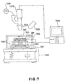
- Figure 7 is a schematic view for illustrating the imprint apparatus.
- the imprint apparatus includes a light source 7000 (halogen lamp), an image pickup device 7010 (CCD: 1.3 megapixels; 12 bit), a lens 7020 (magnification: 10; numerical aperture (NA): 0.28), and an ultraviolet (UV) light source 7030 for during a photocurable resin material.
- the UV light source is inclined with respect to an optical axis of the lens 7020.
- the imprint apparatus further includes a housing 7040 for holding a mold, a mold 7060 provided with an imprint pattern, a wafer substrate 7070 formed of silicon or the like, a vibration isolation table 7080, and a group of stages 7081, 7082, and 7083 which are operable in a perpendicular direction, a lateral direction, and a longitudinal direction, respectively, in order to effect course adjustment. These stages have alignment accuracies of ⁇ 1 ⁇ m or less with respect to XYZ directions and an accuracy of ⁇ 1 m degree or less with respect to ⁇ (a rotation angle about an axis).
- the imprint apparatus further includes a fine adjustment stage 7084 utilizing a piezoelectric element.
- ranges with respect to ⁇ (a rotation axis about x-axis) and ⁇ (a rotation axis about y-axis) are ⁇ 1000 ⁇ rad or less, and a range of ⁇ is ⁇ 800 ⁇ rad.
- the imprint apparatus further includes a computer 7050 for performing signal processing and sending control signals.
- the mold 7060 is formed of quartz and provided in advance with a rectangular or cross alignment mark and a grating with pitch P 1 .
- the mold has a 50 nm-thick surface layer of SiN.
- the alignment mark has grooves having a depth of 166 nm.
- the substrate 7070 formed of silicon wafer is provided with an alignment mark and a grating with pitch P 2 .
- the alignment mark for the substrate has grooves having a depth of 150 nm.
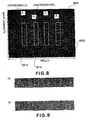
- Figure 8 shows a state in which a mold-side alignment mark 8000 (enclosed by a solid line) and a substrate-side alignment mark 8500 (enclosed by dotted line) observed through an image pickup device overlap each other.
- the mold is also provided with the grating with pitch P 2 .
- the substrate is also provided with the grating with pitch P 1 .
- the gratings with pitches P 1 and P 2 provided each of the substrate and the mold are disposed so as not to optically overlap each other. Further, at mutually nonoverlapping positions, a first area (region) 8010 and a second area (region) 8510 are determined.
- a resist as the photocurable resin is interposed between the mold and the substrate.
- Figure 9(a) shows the first area 8010 extracted from the image data in Figure 8
- Figure 9(b) shows the second area 8050 extracted from the image data in Figure 8 .
- image data are selected and extracted from the first and second areas (steps 2910 and 2920 in Figure 10 ).
- the positional deviation ⁇ is represented by an equation attributable to the positions on the substrate side.
- the equation is used for performing the signal processing on the presumption that the mold-side positions are located at desired positions.
- the computation may also be performed on the presumption that the substrate-side positions are located at desired positions. It is also possible to perform the computation using both of positional deviations d1 and d2 attributable to the positions on the mold side and the substrate side, respectively.
- step 2930 By the computation (step 2930), it is possible to obtain a component of moire fringes represented by the following term (step 2940). cos 2 ⁇ ⁇ ⁇ 1 P 1 - 1 P 2 ⁇ x - 2 ⁇ ⁇ P 2 ⁇ ⁇
- phase component (-(2 ⁇ /P 2 ) ⁇ ) is extracted.
- Figure 11 shows profiles of the moire fringe component, wherein a dotted line 3000 represents the case where there is no out-of-phase component, and a solid line 3010 represents the case where the moire fringe component is actually deviated by the above-described phase component 3500.
- the imprint method is characterized in that when an alignment mark provided to the mold is observed through the image pickup device, a wavelength of light entering the image pickup device is controlled depending on the gap between the mold and the substrate or a thickness of a member constituting the alignment mark. More specifically, in the imprint method, the resin material onto which the pattern is to be transferred is interposed between the mold and the substrate. In the case where refractive indices of the resin material and the mold are close to each other, a phenomenon which is called index matching such that the alignment mark including projections and recesses formed on the mold disappears is caused to occur. In an actual observation, it is difficult to perform the observation of the alignment mark for the mold.
- the gap between the mold and the substrate can be several tens of nanometers to several hundreds of nanometers.
- the contrast of the mark can be lowered by an interference effect of light, thus being required to be further improved.
- the reflectance is largely improved by using SiN as the material for the mold mark.
- the gap between the mold and the substrate and the thickness of the film of the high-refractive index material can be several tens of nanometers to several hundreds of nanometers. In such a case, the light interference effect is remarkably obtained.
- Figure 19 is a graph showing a relationship between a wavelength and a reflected light intensity in the case where the mold mark has a four-layer structure including layers of SiO 2 , SiN, a resin material (thickness (gap): 100 nm), and Si, and a thickness of SiN layer is variable. More specifically, Figure 12 shows a result of simulation with the four-layer structure including an Si layer having an infinite thickness, a 100 nm-thick resin material layer formed on the Si layer, an SiN layer (thickness: 20 nm, 50 nm, 150 nm) formed on the resin material layer, and an SiO 2 layer which has an infinite thickness and is disposed on the SiN layer.
- Calculation of values is made by using a model for Fresnel reflection.
- a three-layer structure including three layers (SiO 2 layer/resin material layer/Si layer) prepared by omitting the SiN layer from the above descried four-layer structure is employed.
- a resultant contrast when the mark is observed is better with a larger difference between the four-layer structure including the SiN layer and the three-layer (reference) structure lacking the SiN layer.
- a reflected light intensity is 0.27 when the SiN layer has a thickness of 50 nm and is 0.11 when the SiN layer has a thickness of 150 nm.
- the reference structure provides a reflected light intensity of 0.11 at the wavelengths of 400 - 800 nm, so that a contrast at the wavelength of 600 nm is increased in the order of the SiN layer thicknesses of 150 nm, 20 nm, and 50 nm.
- a contrast is increased in the order of 20 nm, 50 nm, and 150 nm (SiN layer thickness).
- a contrast is highest at the SiN layer thickness of 20 nm.
- Figure 20 is a graph showing a relationship between a wavelength and a reflected light intensity in the case where the mold mark has a four-layer structure including layers of SiO 2 , SiN (thickness: 50 nm), a resin material, and Si, and a thickness of the resin material layer as a gap layer is variable. More specifically, values of the thickness (gap) are 50 nm, 100 nm, and 200 nm.
- the intensity values are 0.273 for the gap (resin material layer thickness) of 100 nm, 0.099 for the gap of 50 nm, and 0.033 for the gap of 200 nm. Since the intensity of the reference structure is 0.11 at the wavelengths of 400 - 800 nm ( Figure 19 ), a contrast at the wavelength of 600 nm is increased in the order of the gaps of 50 nm, 200 nm, and 100 nm. A contrast at the wavelength of 500 nm is increased in the order of the gaps of 200 nm, 50 nm, and 100 nm. Further, a contrast at the wavelength of 800 nm is increased in the order of the gaps of 100 nm, 50 nm and 200 nm.
- the reflectance is changed depending on the wavelength in the case where the SiN layer thickness or the gap (resin material layer thickness) is several tens of nanometers to several hundreds of nanometers (a fraction of the wavelength of light for observation to several times the wavelength of light for observation). For this reason, it is desirable that the wavelength of light entering the image pickup device is controlled depending on the SiN layer thickness or the gap.
- a contrast is determined by a difference between an average of the spectra in this range and the reference(intensity:0.11).
- the SiN layer has a thickness of 50 nm in this case.
- the mark is observed at the wavelength of 400 - 450 nm.
- the gap is 100 nm in a further approximated state, the mark is observed at the wavelength of 500 - 550 nm.
- the gap is 50 nm in a still further approximated state, the mark is observed at the wavelength of 400 - 450 nm. Even when the gap is another value, the mark is observed at an optimum wavelength.
- a method of selecting the wavelength may be a method using a color filter or a method using a plurality of laser beams.
- the color filter may be disposed on the illumination optical system side or the image pickup device side.
- the apparatus in the case where optical information is inputted into the image pickup device through a wavelength filter, it is possible to always obtain information about an image having a high contrast by changing a transmission wavelength range of the wavelength filter depending on the gap.
- the apparatus includes an image pickup device for observing the mold and a means for controlling a wavelength of light entering the image pickup device depending on a gap between the mold and the substrate.
- the means for controlling the wavelength is constituted by the color filter or a plurality of light sources (capable of outputting light fluxes at a plurality of wavelengths).
- an optical system for observing a first object position at a processing surface of the mold and a second object position at a portion closer, than the processing surface, to a member to be processed is used and alignment between the mold and the member to be processed is effected by using a means for recognizing a relative relationship of (or a difference in) observation position between a first image pickup device for observing the first object position and a second image pickup device for observing the third object position.
- the reference substrate is used as the means for recognizing the difference in observation position.
- the alignment between the mold and the member to be processed is effected by comparing data obtained in advance by the first and second image pickup devices with data (currently) obtained by the first and second image pickup devices. Further, it is also possible to employ a constitution in which the alignment between the mold and the member to be processed is effected by making comparison in each of several areas in image pickup areas of the first and second image pickup devices.
- an optical system for observing a first object position at a processing surface of the mold and a second object position at a portion closer to the member to be processed with respect to the processing surface of the mold is used.
- the processing method can be constituted so that alignment between the mold and the member to be processed is effected by using a means for recognizing a relative relationship of (or a difference in) observation position between a first image pickup device for observing the first object position and a second image pickup device for observing the second object position.
- the processing method includes a step of recognizing the difference in observation position by the reference substrate and a step of effecting the alignment between the member to be processed and the mold at the second object position. Further, it is possible to employ a constitution in which the alignment between the mold and the member to be processed is effected by comparing data obtained in advance by the first and second image pickup devices with data (currently) obtained by the first and second image pickup devices. Further, it is possible to employ a constitution in which the processing method includes a step of selecting a plurality of areas from an image obtained by the first image pickup device, a step of effecting first signal processing in each of the plurality of areas, and a step of effecting second signal processing on the basis of a result of the first signal processing.
- a relative positional relationship between the respective image pickup ranges at two (first and second) object positions is measured or determined with the reference substrate by using the optical system for observing coaxially the two object positions of the mold and the substrate.
- the pattern transfer apparatus can also be constituted as described below.
- the apparatus means a pattern transfer apparatus for transferring the imprinting pattern formed on the mold onto the substrate or the resin material interposed between the substrate and the mold.
- the pattern transfer apparatus includes a first image pickup portion for obtaining an image at a first depth of focus and a second image pickup portion for obtaining an image at a second depth of focus.
- a first alignment mark provided to the mold and a second alignment mold provided to the substrate are disposed within the first depth of focus and observed through the first image pickup portion to obtain a first image.
- a third mark provided to the mold or the substrate is disposed within the second depth of focus and observed through the second image pickup portion to obtain a second image.
- the pattern transfer apparatus is constituted so as to obtain information about a difference in observation range between the first and second image pickup portions by using the first and second images.
- the third alignment mark may be identical to or different from the first alignment mark or the second alignment mark.
- Example 1 an alignment method of the mold and the substrate will be described.
- Figures 12(a) to 12(d) are schematic views for illustrating the alignment method, in this example, of the mold and the substrate in which the reference substrate is used.
- a reference numeral 101 represents a first object position
- a reference numeral 102 represents a second object position
- a reference numeral 103 represents a mold
- a reference numeral 104 represents a mold mark
- a reference numeral 110 represents a reference substrate
- a reference numeral 111 represents a reference substrate mark
- a reference numeral 112 represents a substrate
- a reference numeral 113 represents a substrate mark.
- an optical system for observing the first object position 101 at a processing surface of the mold 103 and the second object position 102 located in the substrate 112 side with respect to the processing surface is used.
- the mold mark 104 and the substrate mark 113 are observable at the same time.
- the first object position and the second object position are spaced, e.g., several nanometers or more apart, so that the mold and the substrate are in a noncontact positional relationship even when the substrate is moved at high speed in an in-plane direction parallel to the processing surface.
- a central view shows a first observation range 106 at the first object position 101.
- a right-hand view shows a second observation range 107 at the third object position 102.
- the first observation range 106 includes a first image pickup range 108 as a portion for image pickup
- the second observation range 107 includes a second image pickup range 109 as a portion for image pickup.
- a.left-hand view shows a cross section, of the mold 103 and the reference substrate 110 or the substrate 112, taken along a vertical bisecting line, such as A-A' line indicated in the central view of Figure 12(a) .
- the reference substrate 110 is used for the alignment between the mold and the substrate.
- a procedure of the alignment method is as follows.
- Figure 12(a) shows a state in which the reference substrate mark 111 is caused to correspond to the mold mark at the first object position 101.
- This state is realized in the following manner.
- the substrate is disposed at a substrate holding portion and the center of the reference substrate mark 111 can be caused to correspond to (the center of) the mold mark 104 by using the in-plane.moving mechanism.
- the alignment (positional adjustment) at this time can be effected with an accuracy on the order of nanometers by using the in-plane moving mechanism.
- the image at the second object position 102 is not particularly required to be used.
- the reference substrate is moved in the negative direction of z-direction by using a substrate hoisting and lowering mechanism so that the reference substrate mark 111 reaches the second object position 102. During this movement, the reference substrate is not deviated in xy-directions. In the resultant state, the reference substrate mark 111 is observed at the second object position 102 and an image in this state is picked up and stored. At this time, the image at the first object position 101 is not particularly required to be used.
- the substrate holding portion holding the substrate 112 is disposed at a designated position (referred to as "F1-1") opposite to the mold 103 by the in-plane moving mechanism.
- the substrate mark 113 is observed at the second object position 102.
- alignment is effected so that the center of the substrate mark 113 is aligned with the center of the reference substrate mark 111 observed at the second object position 102 shown in Figure 12(b) by using the in-plane moving mechanism.
- This alignment can be effected at high speed since the mold and the substrate are placed in a separation state.
- E1-1 A difference (referred to as "E1-1") between the designated position (F1-1) of the substrate holding portion at this time and a designated position of the substrate holding portion after completion of the alignment (referred to as "S1-1") is stored. In this case, it is not particularly necessary to use the image at the first object position 101.
- the substrate 112 is raised in the positive direction of z-direction, so that the substrate 112 is disposed at the first object position 101.
- the mold and the substrate is basically placed in a completion state of alignment.
- imprint is effected by setting a designated position on the presumption that there is the difference (deviation) (E1-1) with respect to subsequent transfer onto the same substrate. In this case, it is not particularly necessary to use the image at the second object position 102.
- the mold and the substrate are deviated from each other and located outside a tolerable range, it is also possible to effect further alignment between the mold and the substrate. This operation may be required, e.g., in the case where the positions of the mold and the substrate are deviated from each other due to a stress, exerted thereon, caused by the contact between the mold and the substrate via the resin material.
- the positional deviation between the mold and the substrate occurs, when an amount of the deviation between the mold and the substrate is identical irrespective of the position of the substrate, the following processing is performed.
- a difference (referred to as "E1-2") between the designated position (F1-1) of the substrate holding portion at that time and a position of the substrate holding portion at the time of completion of the alignment (referred to as "S1-2") is stored.
- the alignment ha.s already been effected at the second object position as shown in Figure 1(c) , so that a value of the difference (E1-2) is not large.
- imprint is effected by setting a designated position on the presumption that there is the difference (deviation) (E1-2) with respect to subsequent transfer onto the same substrate.
- the above described alignment is effected on the entire surface of the substrate on the basis of information about the positional deviation between the mold and the substrate at a certain point of the substrate.
- the reference substrate it is also possible to use the substrate itself onto which the imprinting pattern is to be transferred. However, in this case, there is apprehension that distortion of the substrate during the process and a difference among individual substrates can occur. For this reason, it is desirable that a stable reference substrate is used.
- a reference substrate 201 shown in Figure 13(a) has a square shape and is constituted so that an area 202 having a size equal to a pattern area of the mold is disposed on the reference substrate 201 and four reference substrate marks 203 are disposed at four corners of the area 202.
- a reference substrate 204 shown in Figure 13(b) has a circular shape and is constitute so as to have a size equal to that of the substrate onto which the imprinting pattern is to be transferred.
- On the reference substrate 204 there are a pattern are 205 in which reference substrate marks are provided and a pattern area 206 in which no reference substrate mark is provided. In this constitution, correction of the positional deviation can be made at several positions at which the reference substrate mark is provided.
- a reference substrate 207 shown in Figure 13(c) is constituted by the substrate itself onto which the imprinting pattern is to be transferred. In this case, the correction may be made at all of positions in pattern areas or at the several positions shown in Figure 13(b) .
- a mold mark 310 is formed as an image on the first image pickup device 307 and a second mark 311 is formed as an image on the second image pickup device 308.
- An image of the first object position 313 is formed on the first image pickup device 307 and an image of the second object position 314 is formed on the second image pickup device 308.
- the processing apparatus includes an exposure light source 401, a body tube 402, a mold holding portion 403, a substrate holding portion 404, a substrate hoisting and lowering mechanism (z-direction) 405, an in-plane moving mechanism (xy-directions) 406, the optical system for measurement shown in Figure 14 , image pickup devices 408, and an analyzing mechanism 409.
- the mold holding portion 403 effects chucking of a mold 411 according to a vacuum chucking method.or the like.
- a substrate 412 is movable to a desired position by the in-plane moving mechanism 406. Further, by the substrate hoisting and lowering mechanism 405, adjustment of a height of the substrate 412 and application of pressure can be effected.
- the in-plane moving mechanism 406 and the substrate hoisting and lowering mechanism 405 are subjected to measurement of distance by an interferometer or the like with a control accuracy on the order of subnanometers. Control of positional movement of the substrate, pressure application, exposure and the like is made by an imprint control mechanism 410.
- Example 2 a method of alignment between the mold and the substrate different from the alignment method of Example1 will be described.
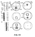
- Figures 16(a) to 16(c) include schematic views for illustrating a mold of alignment between a mold. 502 and a substrate 513.
- a first reference substrate mark 506 and a second reference substrate mark 504 are disposed, respectively. Further, an optical thickness of the reference substrate 505 is made equal to a distance between a first object position 501 and a second object position 503. Based on these features, it is possible to determine a position, to which a substrate mark should be moved at a second object position in order to align the substrate mark with a desired position of a mold mark at a first object position, at one time as described below.
- Figure 16(a) includes schematic views showing the case where the first reference substrate mark 506 of the reference substrate 505 is located at a first object position 501. Further, the second reference substrate mark 504 is located at a second object position 503. The first reference substrate mark 506 is disposed in a first image pickup area 510 provided in a first observation area 509. Further, the second reference substrate mark 504 is disposed in a second pickup area 512 provided in a second observation area 511. A reference numeral 508 represents a difference between center positions in the first and second image pickup ranges 510 and 512.
- the reference substrate 505 is disposed on a substrate holding portion (not shown) and on the basis of a mold mark 507, alignment (positional adjustment) of the first reference substrate mark 506 is effected at the first object position 501 by an in-plane moving mechanism. More specifically, e.g., the alignment is effected so that the center of the first reference substrate mark 507 and the center of the mold mark 506 coincide with each other. At this time, at the second object position 503, the second reference substrate mark 504 is located and an image thereof is stored.
- the reference substrate 505 is removed from the substrate holding portion.
- the substrate holding portion holding the substrate is disposed at a designated position (referred to as "F2-1") opposite to the mold by the in-plane moving mechanism.
- F2-1 a designated position
- a first substrate mark 514 and a second substrate mark 515 are observed at the second object position.
- alignment is effected so that the center of the first substrate mark 514 is aligned with the center of the reference substrate mark 504 observed at the second object position 503 shown in Figure 16(a) by using the in-plane moving mechanism.
- a difference (referred to as "E2-1") between the designated position. (F2-1) of the substrate holding portion at this time and a designated position of the substrate holding portion after completion of the alignment (referred to as "S2-1") is stored.
- Figure 16(c) shows a state in which the substrate holding portion holding the substrate is raised, so that the first and second substrate marks 514 and 515 are disposed at the first object position 501.
- alignment between the mold and the substrate is ordinarily completed.
- imprint is effected by setting a designated position on the presumption that there is the difference (deviation) (E2-1) with respect to subsequent transfer onto the same substrate.
- the second substrate mark 515 is positionally aligned on the basis of the mold mark 507 at the first object position 501 shown in Figure 16(c) by using the in-plane moving mechanism.
- the alignment at the second object position 503 shown in Figure 16(b) has already been effected, so that a degree of the positional deviation is not large.
- a difference (referred to as "E2-2") between the designated position (F2-1) of the substrate holding portion and a position of the substrate holding portion at the time of completion of the alignment (referred to as "S2-2") is stored. Thereafter, imprint is effected by setting a designated position on the presumption that there is the difference (deviation) (E2-2) with respect to subsequent transfer onto the same substrate.
- Example 3 a method of alignment between the mold and the substrate different in image processing method from the alignment method of Example 1 will be described.
- Figures 17(a) to 17(c) include schematic views for illustrating an image processing method in this example.
- Figure 17(a) shows a state in which a reference substrate mark 614 of the reference substrate 613 is located at the first object position 601.
- a first area A 610 is designated as an area including a mold mark 604 of a mold 602 on the basis of the mold mark 604.
- a first area B 611 and a first area C 613 are designated with a certain distance (interval) between adjacent areas.
- the reference substrate mark 614 is positionally adjusted with respect to the first area C 613 by being moved by an in-plane moving mechanism.
- the first area C is disposed at a desired position by effecting signal processing such that the first area A 610 and the first area C 612 are selected or extracted from an image, subjected to contrast adjustment for each extracted image, and the two extracted images are superposed.
- the reference substrate 613 is lowered by a substrate hoisting and lowering mechanism to a second object position 603 at which the reference substrate mark 604 is observed.
- a reference numeral 606 represents a difference between center positions in first and second image pickup ranges 608 and 609.
- Figure 17(b) shows a state in which the reference substrate mark 604 of the reference substrate 613 is located at the second object position 603.
- a second area C 617 is designated on the basis of the reference substrate mark 604 so as to include the reference substrate mark 604. Thereafter, a second area B 616 and a second area A 615 are designated with a certain distance (interval) between adjacent areas. Thereafter, the reference substrate 505 is removed from the substrate holding portion.
- Figure 17(c) includes views for illustrating the case where a substrate 618 is observed at the second object position 603.
- the substrate holding portion holding the substrate is disposed at a designated position (referred to as "F3-1") opposite to the mold by the in-plane moving mechanism.
- F3-1 a designated position
- a substrate mark 619 is observed at the second object position.
- the second area B 616 is selected or extracted from an image and superposed on an image of the second area C 617 obtained in the operation described with reference to Figure 17(b) to effect positional adjustment.
- This positional adjustment can be performed at high speed since the contact between the mold and the substrate is not generated at this time.
- the respective images are subjected to signal processing such as contrast adjustment or the like in advance.
- Figure 17(d) shows a state in which the substrate 618 is raised in the positive direction of z-direction by the hoisting and lowering mechanism to dispose the substrate mark 619 at the first object position 601.
- the alignment between the mold 602 and the substrate 618 is ordinarily completed, so that a resultant positional deviation is expected to be a level within a tolerable range.
- a difference (referred to as "E3-1") between the designated position (F3-1) of the substrate holding portion at this time and a designated position of the substrate holding portion after completion of the alignment (referred to as "S3-1") is stored. Thereafter, imprint is effected by setting a designated position on the presumption that there is the difference (deviation) (E3-1) with respect to subsequent transfer onto the same substrate.
- an effect of using different areas in the image pickup area of the image pickup device is that reflectances of the mold and the substrate are different from each other and thus the images of the mold and the substrate can be independently subjected to signal processing to facilitate an increase in accuracy of alignment. Further, it is not necessary to consider an influence of mutual interference since the mold and the substrate are not vertically overlaid on each other, so that a degree of freedom of the mark can be increased.
- Figures 18(a) to 18(f) are schematic views for illustrating alignment marks used when alignment is effected by image-processing moire fringes in Example 3.
- Figure 18(a) shows a first mark including a bar pattern 701 with a pitch P 1 and a bar pattern 702 with a pitch P 2 .
- Figure 18(b) shows a second mark including the bar pattern 701 with the pitch P 1 and a bar pattern with the pitch P 2 , wherein the bar patterns 701 and 702 have an arrangement opposite to that of the bar patterns 701 and 702 in the first mark shown in Figure 18(a) .
- a composite image 706 as shown in Figure 18(c) is formed. In this composite image 706, left-hand and right-hand moire fringes are in phase with each other.
- Figure 18(c) shows a state in which alignment between the mark and the substrate is completed.
- the left-hand and right-hand moire images are out of phase with each other.
- the moire fringes have a period equal to a pitch P M represented by the following equation.
- P M P 1 ⁇ P 2 P 1 - P 2
- the moire fringes are arranged to constitute a first mark 709 for XY ⁇ measurement as shown in Figure 18(d) , wherein the first mark 709 includes a first area 710, a second area 711, a third area 712, a fourth area 713, a pattern 707 with a pitch P 3 , and a pattern 708 with a pitch P 4 .
- the moire fringes are arranged to constitute a second mark 714 for XY ⁇ measurement as shown in Figure 18(e) , wherein the second mark 714 includes the first to fourth areas 710 - 713 and the patterns 707 and 708 which are arranged opposite to those in Figure 18(d) .
- FIG. 18(f) shows a composite image 716 for XY ⁇ measurement including moire fringes 715 for XY ⁇ measurement at the time after the alignment is completed.
Landscapes
- Engineering & Computer Science (AREA)
- Physics & Mathematics (AREA)
- General Physics & Mathematics (AREA)
- Chemical & Material Sciences (AREA)
- Nanotechnology (AREA)
- Crystallography & Structural Chemistry (AREA)
- Condensed Matter Physics & Semiconductors (AREA)
- Manufacturing & Machinery (AREA)
- Multimedia (AREA)
- Mathematical Physics (AREA)
- Theoretical Computer Science (AREA)
- Mechanical Engineering (AREA)
- Shaping Of Tube Ends By Bending Or Straightening (AREA)
- Exposure Of Semiconductors, Excluding Electron Or Ion Beam Exposure (AREA)
- Length Measuring Devices By Optical Means (AREA)
- Micromachines (AREA)
- Moulds For Moulding Plastics Or The Like (AREA)
Claims (6)
- Ausrichtungsverfahren zur Bewirkung einer Ausrichtung zwischen ersten und zweiten plattenartigen Objekten (309, 312) unter Verwendung von Moire-Interferenzmustern, die erhalten werden, indem eine erste periodische Struktur (701) mit einem ersten Abstand (P1), die auf dem ersten Objekt (309) bereitgestellt ist, und eine zweite periodische Struktur (702) mit einem zweiten Abstand (P2), die auf dem zweiten Objekt (312) bereitgestellt ist, durch eine Bildaufnahmevorrichtung (307) beobachtet werden, wobei das Ausrichtungsverfahren umfasst:ein Bereitstellen der ersten periodischen Struktur (701) und der zweiten periodischen Struktur (702) auf dem ersten Objekt (309) bzw. dem zweiten Objekt (312) bei Positionen, bei denen die erste periodische Struktur (701) und die zweite periodische Struktur (702) in einer wechselweise nicht-überlappender Art und Weise in einem Bildaufnahmebereich der Bildaufnahmevorrichtung (307) beobachtet werden,ein Aufnehmen (S-1) von Bildern der ersten und zweiten periodischen Strukturen (701, 702) unter Verwendung der Bildaufnahmevorrichtung (307), um erste Bildinformationen eines ersten Bereichs (A), der die erste periodische Struktur (701) umfasst, und zweite Bildinformationen eines zweiten Bereichs (B), der die zweite periodische Struktur (702) umfasst, zu erhalten, undein Bewirken (S-3, S-4, S-5) einer Ausrichtung zwischen den ersten und zweiten Objekten (309, 312), indem Grundfrequenzen, die den ersten und zweiten periodischen Strukturen (701, 702) entsprechen, von den erhaltenen ersten Informationen bzw. den erhaltenen zweiten Informationen extrahiert werden, eine Berechnung mit den Grundfrequenzen ausgeführt wird, um eine Moire-Interferenzmusterkomponente zu extrahieren, und Informationen über eine Positionsabweichung zwischen den ersten und zweiten Objekten (309, 312), die von der Moire-Interferenzmusterkomponente erhalten werden, verwendet werden.
- Verfahren nach Anspruch 1, wobei ein Bereich des ersten Bereichs (A) gleich zu dem des zweiten Bereichs (B) ist.
- Verfahren nach Anspruch 1, wobei, wenn der Bereich des ersten Bereichs (A) unterschiedlich zu dem des zweiten Bereichs (B) ist, eine Bildverarbeitung derart ausgeführt wird, dass der Bereich des ersten Bereichs (A) gleich dem des zweiten Bereichs (B) ist, nachdem die ersten Bildinformationen des ersten Bereichs (A) und die zweiten Bildinformationen des zweiten Bereichs (B) erhalten worden sind.
- Verfahren nach einem der Ansprüche 1 bis 3, wobei die Berechnung ausgeführt wird, indem eine Multiplikation der Grundfrequenzen, die den ersten und zweiten periodischen Strukturen (701, 702) entsprechen, ausgeführt wird.
- Verfahren nach einem der Ansprüche 1 bis 4, wobei jedes des ersten Objekts (309) und des zweiten Objekts (312) die erste periodische Struktur (701) und die zweite periodische Struktur (702) bei Positionen aufweist, in denen die erste periodische Struktur (701) und die zweite periodische Struktur (702) in der wechselweise nicht-überlappenden Art und Weise beobachtet werden, und
wobei die Moire-Interferenzmusterkomponente von der ersten periodischen Struktur (701) des ersten Objekts (309) und der zweiten periodischen Struktur (702) des zweiten Objekts (312) extrahiert wird und von der zweiten periodischen Struktur (702) des ersten Objekts (309) und der ersten periodischen Struktur (701) des zweiten Objekts (312) extrahiert wird. - Verfahren nach einem der Ansprüche 1 bis 5, wobei das erste Objekt (309) eine Form ist und das zweite Objekt (312) ein Substrat ist, und
wobei die Ausrichtung in Bezug auf eine in der Ebene liegende Richtung des Substrats bewirkt wird.
Applications Claiming Priority (4)
| Application Number | Priority Date | Filing Date | Title |
|---|---|---|---|
| JP2006114093 | 2006-04-18 | ||
| JP2006305239 | 2006-11-10 | ||
| JP2007036598 | 2007-02-16 | ||
| PCT/JP2007/058898 WO2007123249A2 (en) | 2006-04-18 | 2007-04-18 | Alignment method, imprint method, alignment apparatus, and position measurement method |
Publications (2)
| Publication Number | Publication Date |
|---|---|
| EP2010966A2 EP2010966A2 (de) | 2009-01-07 |
| EP2010966B1 true EP2010966B1 (de) | 2012-08-01 |
Family
ID=38226383
Family Applications (1)
| Application Number | Title | Priority Date | Filing Date |
|---|---|---|---|
| EP07742333A Not-in-force EP2010966B1 (de) | 2006-04-18 | 2007-04-18 | Aurichtungsverfahren |
Country Status (6)
| Country | Link |
|---|---|
| US (1) | US8845317B2 (de) |
| EP (1) | EP2010966B1 (de) |
| JP (2) | JP4795300B2 (de) |
| KR (1) | KR101045434B1 (de) |
| CN (1) | CN102053490B (de) |
| WO (1) | WO2007123249A2 (de) |
Families Citing this family (62)
| Publication number | Priority date | Publication date | Assignee | Title |
|---|---|---|---|---|
| GB0622691D0 (en) * | 2006-11-14 | 2006-12-27 | Airbus Uk Ltd | Method and apparatus for controlling the geometry of a composite component |
| US7837907B2 (en) * | 2007-07-20 | 2010-11-23 | Molecular Imprints, Inc. | Alignment system and method for a substrate in a nano-imprint process |
| US8237133B2 (en) * | 2008-10-10 | 2012-08-07 | Molecular Imprints, Inc. | Energy sources for curing in an imprint lithography system |
| US8628712B2 (en) * | 2008-10-27 | 2014-01-14 | Molecular Imprints, Inc. | Misalignment management |
| US8345242B2 (en) | 2008-10-28 | 2013-01-01 | Molecular Imprints, Inc. | Optical system for use in stage control |
| NL2003871A (en) * | 2009-02-04 | 2010-08-05 | Asml Netherlands Bv | Imprint lithography. |
| NL2004932A (en) * | 2009-07-27 | 2011-01-31 | Asml Netherlands Bv | Imprint lithography template. |
| JP5800456B2 (ja) * | 2009-12-16 | 2015-10-28 | キヤノン株式会社 | 検出器、インプリント装置及び物品の製造方法 |
| NL2005975A (en) | 2010-03-03 | 2011-09-06 | Asml Netherlands Bv | Imprint lithography. |
| JP2011209064A (ja) * | 2010-03-29 | 2011-10-20 | Fuji Xerox Co Ltd | 物品認識装置及びこれを用いた物品処理装置 |
| JP2011209959A (ja) * | 2010-03-29 | 2011-10-20 | Fuji Xerox Co Ltd | 組付受部品の認識構造及びこれを用いた組立情報認識装置並びに組立処理装置 |
| JP5539011B2 (ja) * | 2010-05-14 | 2014-07-02 | キヤノン株式会社 | インプリント装置、検出装置、位置合わせ装置、及び物品の製造方法 |
| US9864279B2 (en) * | 2010-08-05 | 2018-01-09 | Asml Netherlands B.V. | Imprint lithography |
| JP5850717B2 (ja) * | 2010-12-02 | 2016-02-03 | キヤノン株式会社 | インプリント装置、及びそれを用いた物品の製造方法 |
| JP5776266B2 (ja) * | 2011-03-29 | 2015-09-09 | 大日本印刷株式会社 | インプリント方法およびそれを実施するためのインプリント装置 |
| US9182627B2 (en) * | 2011-04-11 | 2015-11-10 | Engineering System Co., Ltd. | Liquid-discharging device with observation optical system |
| JP6306501B2 (ja) * | 2011-04-25 | 2018-04-04 | キヤノン ナノテクノロジーズ,インコーポレーテッド | テンプレートおよびテンプレートを基板と位置合わせするための方法 |
| JP5637931B2 (ja) * | 2011-05-17 | 2014-12-10 | キヤノン株式会社 | インプリント装置、インプリント方法およびデバイス製造方法 |
| JP5864929B2 (ja) * | 2011-07-15 | 2016-02-17 | キヤノン株式会社 | インプリント装置および物品の製造方法 |
| US9213227B2 (en) * | 2011-08-18 | 2015-12-15 | Nikon Corporation | Custom color or polarization sensitive CCD for separating multiple signals in autofocus projection system |
| JP6159072B2 (ja) | 2011-11-30 | 2017-07-05 | キヤノン株式会社 | インプリント装置、インプリント方法及び物品の製造方法 |
| KR101414830B1 (ko) * | 2011-11-30 | 2014-07-03 | 다이닛뽕스크린 세이조오 가부시키가이샤 | 얼라이먼트 방법, 전사 방법 및 전사장치 |
| JP5901655B2 (ja) * | 2011-12-22 | 2016-04-13 | キヤノン株式会社 | インプリント装置及びデバイス製造方法 |
| JP6045363B2 (ja) | 2012-01-27 | 2016-12-14 | キヤノン株式会社 | インプリント装置、それを用いた物品の製造方法 |
| JP5832345B2 (ja) * | 2012-03-22 | 2015-12-16 | 株式会社ニューフレアテクノロジー | 検査装置および検査方法 |
| JP5793457B2 (ja) * | 2012-03-26 | 2015-10-14 | 株式会社Screenホールディングス | 転写方法および転写装置 |
| JP2013222791A (ja) * | 2012-04-16 | 2013-10-28 | Fujifilm Corp | ナノインプリント方法およびナノインプリント用基板並びにそれらを用いたパターン化基板の製造方法 |
| US9190100B2 (en) * | 2012-04-25 | 2015-11-17 | Seagate Technology | Determining at least one of alignment and bond line thickness between an optical component and a mounting surface |
| JP6039917B2 (ja) * | 2012-05-22 | 2016-12-07 | キヤノン株式会社 | インプリント装置、インプリント方法及び物品の製造方法 |
| NL2010971A (en) * | 2012-07-10 | 2014-01-13 | Asml Netherlands Bv | Lithographic cluster system, method for calibrating a positioning device of a lithographic apparatus and measurement apparatus. |
| JP2014203917A (ja) * | 2013-04-03 | 2014-10-27 | 株式会社ディスコ | 板状物 |
| JP5909210B2 (ja) * | 2013-07-11 | 2016-04-26 | キヤノン株式会社 | インプリント装置及び物品の製造方法 |
| JP6420606B2 (ja) * | 2013-11-05 | 2018-11-07 | キヤノン株式会社 | インプリント装置、インプリント方法及び物品製造方法 |
| JP6097704B2 (ja) * | 2014-01-06 | 2017-03-15 | キヤノン株式会社 | インプリント装置、インプリント方法及び物品の製造方法 |
| JP6294680B2 (ja) | 2014-01-24 | 2018-03-14 | キヤノン株式会社 | インプリント装置、および物品の製造方法 |
| KR101986258B1 (ko) | 2014-08-29 | 2019-06-07 | 에이에스엠엘 네델란즈 비.브이. | 메트롤로지 방법, 타겟 및 기판 |
| JP5800977B2 (ja) * | 2014-10-23 | 2015-10-28 | キヤノン株式会社 | インプリント装置、インプリント方法およびデバイス製造方法 |
| KR101980464B1 (ko) * | 2014-12-12 | 2019-05-20 | 캐논 가부시끼가이샤 | 임프린트 장치, 임프린트 방법 및 물품의 제조 방법 |
| JP6537277B2 (ja) * | 2015-01-23 | 2019-07-03 | キヤノン株式会社 | インプリント装置、物品製造方法 |
| US10248018B2 (en) * | 2015-03-30 | 2019-04-02 | Canon Kabushiki Kaisha | Imprint apparatus and method of manufacturing article |
| JP6138189B2 (ja) | 2015-04-08 | 2017-05-31 | キヤノン株式会社 | インプリント装置および物品の製造方法 |
| JP2016225433A (ja) * | 2015-05-29 | 2016-12-28 | キヤノン株式会社 | モールド、インプリント方法、インプリント装置および物品の製造方法 |
| JP6039770B2 (ja) * | 2015-08-27 | 2016-12-07 | キヤノン株式会社 | インプリント装置およびデバイス製造方法 |
| JP6685821B2 (ja) * | 2016-04-25 | 2020-04-22 | キヤノン株式会社 | 計測装置、インプリント装置、物品の製造方法、光量決定方法、及び、光量調整方法 |
| JP6758967B2 (ja) * | 2016-07-12 | 2020-09-23 | キヤノン株式会社 | インプリント装置、インプリント方法、及び物品の製造方法 |
| JP6971567B2 (ja) * | 2016-12-16 | 2021-11-24 | キヤノン株式会社 | 位置合わせ装置、位置合わせ方法、リソグラフィ装置、および物品製造方法 |
| EP3339959A1 (de) | 2016-12-23 | 2018-06-27 | ASML Netherlands B.V. | Verfahren zur bestimmung einer position eines merkmals |
| JP7025132B2 (ja) * | 2017-06-05 | 2022-02-24 | キヤノン株式会社 | インプリント装置及び物品の製造方法 |
| KR101943880B1 (ko) * | 2017-06-13 | 2019-04-18 | 주식회사 에이치비테크놀러지 | 표면과 하면에 형성된 패턴간의 상대위치를 결정하는 검사장치 |
| JP6863836B2 (ja) * | 2017-06-28 | 2021-04-21 | キオクシア株式会社 | ナノインプリント用テンプレート及び集積回路装置の製造方法 |
| US11175598B2 (en) * | 2017-06-30 | 2021-11-16 | Canon Kabushiki Kaisha | Imprint apparatus and method of manufacturing article |
| JP7041489B2 (ja) * | 2017-10-19 | 2022-03-24 | キヤノン株式会社 | 評価方法、決定方法、リソグラフィ装置、およびプログラム |
| JP7030533B2 (ja) * | 2018-01-15 | 2022-03-07 | キオクシア株式会社 | インプリント装置、インプリント方法、及び半導体装置の製造方法 |
| JP7116605B2 (ja) * | 2018-06-28 | 2022-08-10 | キヤノン株式会社 | インプリント材のパターンを形成するための方法、インプリント装置、インプリント装置の調整方法、および、物品製造方法 |
| KR102737510B1 (ko) * | 2019-09-18 | 2024-12-05 | 삼성전자주식회사 | 다이 본더 |
| JP6977912B1 (ja) * | 2020-02-06 | 2021-12-08 | 大日本印刷株式会社 | マーカー、マーカーの製造方法、検出対象物 |
| JP7636906B2 (ja) * | 2021-02-22 | 2025-02-27 | キヤノン株式会社 | 計測装置、リソグラフィ装置、および物品の製造方法 |
| US11815811B2 (en) | 2021-03-23 | 2023-11-14 | Canon Kabushiki Kaisha | Magnification ramp scheme to mitigate template slippage |
| CN113910502B (zh) * | 2021-09-15 | 2024-03-26 | 明阳智慧能源集团股份公司 | 一种基于激光跟踪仪的风电叶片模具安装方法 |
| US12124165B2 (en) | 2021-10-25 | 2024-10-22 | Canon Kabushiki Kaisha | Apparatus and method for optimizing actuator forces |
| EP4390540A1 (de) * | 2022-12-19 | 2024-06-26 | Koninklijke Philips N.V. | Ausrichtungsverfahren |
| AT527414B1 (de) * | 2024-01-16 | 2025-02-15 | Univ Linz | Verfahren zur Detektion von Positionsabweichungen |
Family Cites Families (47)
| Publication number | Priority date | Publication date | Assignee | Title |
|---|---|---|---|---|
| JPS59172724A (ja) * | 1983-03-22 | 1984-09-29 | Canon Inc | マーク検出装置 |
| EP0135597B1 (de) * | 1983-09-23 | 1987-07-22 | Ibm Deutschland Gmbh | Verfahren und Einrichtung zum gegenseitigen Ausrichten von Objekten |
| US4883359A (en) * | 1984-02-28 | 1989-11-28 | Canon Kabushiki Kaisha | Alignment method and pattern forming method using the same |
| JPS62208630A (ja) * | 1986-03-10 | 1987-09-12 | Canon Inc | 露光装置 |
| JPS62262426A (ja) * | 1986-05-09 | 1987-11-14 | Canon Inc | 露光装置 |
| JPH0650714B2 (ja) * | 1986-07-17 | 1994-06-29 | キヤノン株式会社 | 露光方法 |
| JPH02292813A (ja) * | 1989-05-02 | 1990-12-04 | Canon Inc | 自動焦点合せ装置 |
| US5585923A (en) * | 1992-11-14 | 1996-12-17 | Canon Kabushiki Kaisha | Method and apparatus for measuring positional deviation while correcting an error on the basis of the error detection by an error detecting means |
| JP3428705B2 (ja) * | 1993-10-20 | 2003-07-22 | キヤノン株式会社 | 位置検出装置及びそれを用いた半導体素子の製造方法 |
| GB9323978D0 (en) | 1993-11-22 | 1994-01-12 | Dek Printing Machines Ltd | Alignment systems |
| JP3292022B2 (ja) * | 1996-01-17 | 2002-06-17 | キヤノン株式会社 | 位置検出装置及びそれを用いた半導体素子の製造方法 |
| JPH1012530A (ja) * | 1996-06-26 | 1998-01-16 | Nikon Corp | アライメント装置 |
| JPH1022213A (ja) * | 1996-06-28 | 1998-01-23 | Canon Inc | 位置検出装置及びそれを用いたデバイスの製造方法 |
| JP3445100B2 (ja) * | 1997-06-02 | 2003-09-08 | キヤノン株式会社 | 位置検出方法及び位置検出装置 |
| JP4208277B2 (ja) * | 1997-11-26 | 2009-01-14 | キヤノン株式会社 | 露光方法及び露光装置 |
| JPH11241908A (ja) * | 1997-12-03 | 1999-09-07 | Canon Inc | 位置検出装置及びそれを用いたデバイスの製造方法 |
| JP3336955B2 (ja) | 1998-05-26 | 2002-10-21 | ウシオ電機株式会社 | 裏面アライメント機能を備えた露光装置 |
| JP4323636B2 (ja) * | 1999-09-21 | 2009-09-02 | キヤノン株式会社 | 位置計測方法及び位置計測装置 |
| JP2001345250A (ja) * | 2000-06-01 | 2001-12-14 | Canon Inc | 位置合せ方法、位置合せ装置、プロファイラ、露光装置、半導体デバイス製造方法、半導体製造工場、および露光装置の保守方法 |
| JP4511786B2 (ja) * | 2000-07-16 | 2010-07-28 | ボード・オブ・リージエンツ,ザ・ユニバーシテイ・オブ・テキサス・システム | 基板とこの基板から離れたテンプレートを整列させる方法 |
| EP1303793B1 (de) * | 2000-07-17 | 2015-01-28 | Board Of Regents, The University Of Texas System | Verfahren und gerät zur automatischen zufuhr von flüssigen materialien in der imprint-lithogrpahie |
| US7317531B2 (en) * | 2002-12-05 | 2008-01-08 | Kla-Tencor Technologies Corporation | Apparatus and methods for detecting overlay errors using scatterometry |
| KR101031528B1 (ko) * | 2000-10-12 | 2011-04-27 | 더 보드 오브 리전츠 오브 더 유니버시티 오브 텍사스 시스템 | 실온 저압 마이크로- 및 나노- 임프린트 리소그래피용템플릿 |
| US6607527B1 (en) * | 2000-10-17 | 2003-08-19 | Luis Antonio Ruiz | Method and apparatus for precision laser surgery |
| US6955767B2 (en) * | 2001-03-22 | 2005-10-18 | Hewlett-Packard Development Company, Lp. | Scanning probe based lithographic alignment |
| JP2002353099A (ja) * | 2001-05-22 | 2002-12-06 | Canon Inc | 位置検出方法及び装置及び露光装置及びデバイス製造方法 |
| JP4803901B2 (ja) * | 2001-05-22 | 2011-10-26 | キヤノン株式会社 | 位置合わせ方法、露光装置、および半導体デバイス製造方法 |
| US20050064344A1 (en) * | 2003-09-18 | 2005-03-24 | University Of Texas System Board Of Regents | Imprint lithography templates having alignment marks |
| JP4006217B2 (ja) * | 2001-10-30 | 2007-11-14 | キヤノン株式会社 | 露光方法、露光装置及びデバイスの製造方法 |
| JP3603880B2 (ja) * | 2002-05-20 | 2004-12-22 | 株式会社日立製作所 | 重ね露光方法 |
| MY164487A (en) * | 2002-07-11 | 2017-12-29 | Molecular Imprints Inc | Step and repeat imprint lithography processes |
| AU2003261317A1 (en) * | 2002-08-01 | 2004-02-23 | Molecular Imprints, Inc. | Scatterometry alignment for imprint lithography |
| JP4095391B2 (ja) * | 2002-09-24 | 2008-06-04 | キヤノン株式会社 | 位置検出方法 |
| JP4072408B2 (ja) * | 2002-09-24 | 2008-04-09 | キヤノン株式会社 | 位置検出方法 |
| JP3448826B2 (ja) | 2002-12-12 | 2003-09-22 | 株式会社ニコン | 位置合わせ方法、露光方法、及びデバイス製造方法 |
| KR100495428B1 (ko) * | 2003-06-27 | 2005-06-14 | 삼성전자주식회사 | 반도체 기판의 정렬 검사방법 |
| US7136150B2 (en) | 2003-09-25 | 2006-11-14 | Molecular Imprints, Inc. | Imprint lithography template having opaque alignment marks |
| JP2005116978A (ja) * | 2003-10-10 | 2005-04-28 | Sumitomo Heavy Ind Ltd | ナノインプリント装置及び方法 |
| JP4677183B2 (ja) * | 2003-12-05 | 2011-04-27 | キヤノン株式会社 | 位置検出装置、および露光装置 |
| JP4538782B2 (ja) * | 2004-01-09 | 2010-09-08 | 株式会社ニコン | 撮像装置 |
| JP4574240B2 (ja) * | 2004-06-11 | 2010-11-04 | キヤノン株式会社 | 加工装置、加工方法、デバイス製造方法 |
| TWI340875B (en) * | 2004-08-10 | 2011-04-21 | Asml Netherlands Bv | Imprint lithographic apparatus, device manufacturing method and device manufactured thereby |
| US7309225B2 (en) * | 2004-08-13 | 2007-12-18 | Molecular Imprints, Inc. | Moat system for an imprint lithography template |
| US7609858B2 (en) * | 2004-08-31 | 2009-10-27 | Hewlett-Packard Development Company, L.P. | Displacement measurements using phase changes |
| JP2007299909A (ja) * | 2006-04-28 | 2007-11-15 | Nsk Ltd | 半導体ウェハ撮像装置 |
| US7612882B2 (en) * | 2006-10-20 | 2009-11-03 | Hewlett-Packard Development Company, L.P. | Optical gratings, lithography tools including such optical gratings and methods for using same for alignment |
| WO2008099795A2 (en) * | 2007-02-06 | 2008-08-21 | Canon Kabushiki Kaisha | Imprint method and imprint apparatus |
-
2007
- 2007-04-17 JP JP2007108341A patent/JP4795300B2/ja not_active Expired - Fee Related
- 2007-04-18 WO PCT/JP2007/058898 patent/WO2007123249A2/en not_active Ceased
- 2007-04-18 EP EP07742333A patent/EP2010966B1/de not_active Not-in-force
- 2007-04-18 CN CN201010539354.5A patent/CN102053490B/zh not_active Expired - Fee Related
- 2007-04-18 US US11/719,878 patent/US8845317B2/en not_active Expired - Fee Related
- 2007-04-18 KR KR1020087028097A patent/KR101045434B1/ko not_active Expired - Fee Related
-
2011
- 2011-04-18 JP JP2011092154A patent/JP5591173B2/ja not_active Expired - Fee Related
Also Published As
| Publication number | Publication date |
|---|---|
| US20090108483A1 (en) | 2009-04-30 |
| CN102053490A (zh) | 2011-05-11 |
| WO2007123249A2 (en) | 2007-11-01 |
| JP4795300B2 (ja) | 2011-10-19 |
| JP2008221822A (ja) | 2008-09-25 |
| CN102053490B (zh) | 2014-02-05 |
| US8845317B2 (en) | 2014-09-30 |
| KR20090009874A (ko) | 2009-01-23 |
| KR101045434B1 (ko) | 2011-06-30 |
| WO2007123249A3 (en) | 2008-05-22 |
| EP2010966A2 (de) | 2009-01-07 |
| JP2011181944A (ja) | 2011-09-15 |
| JP5591173B2 (ja) | 2014-09-17 |
Similar Documents
| Publication | Publication Date | Title |
|---|---|---|
| EP2010966B1 (de) | Aurichtungsverfahren | |
| EP1847875B1 (de) | Musterübertragungsvorrichtung, Druckvorrichtung und Musterübertragungsverfahren | |
| CN101427185B (zh) | 对准方法、压印方法、对准设备和压印设备 | |
| EP1731963B1 (de) | Stempel, Strukturbildungsverfahren, und Apparat zur Strukturbildung | |
| EP1817545B1 (de) | Interferometrische analyse zur herstellung von vorrichtungen in nanogrösse | |
| US7630067B2 (en) | Interferometric analysis method for the manufacture of nano-scale devices | |
| JP6071221B2 (ja) | インプリント装置、モールド、インプリント方法及び物品の製造方法 | |
| White et al. | Novel alignment system for imprint lithography | |
| EP2090928A2 (de) | Druckgerät, Druckverfahren und Druckform |
Legal Events
| Date | Code | Title | Description |
|---|---|---|---|
| PUAI | Public reference made under article 153(3) epc to a published international application that has entered the european phase |
Free format text: ORIGINAL CODE: 0009012 |
|
| 17P | Request for examination filed |
Effective date: 20081124 |
|
| AK | Designated contracting states |
Kind code of ref document: A2 Designated state(s): AT BE BG CH CY CZ DE DK EE ES FI FR GB GR HU IE IS IT LI LT LU LV MC MT NL PL PT RO SE SI SK TR |
|
| AX | Request for extension of the european patent |
Extension state: AL BA HR MK RS |
|
| 17Q | First examination report despatched |
Effective date: 20090903 |
|
| REG | Reference to a national code |
Ref country code: DE Ref legal event code: R079 Ref document number: 602007024343 Country of ref document: DE Free format text: PREVIOUS MAIN CLASS: G03F0009000000 Ipc: G03F0007000000 |
|
| GRAP | Despatch of communication of intention to grant a patent |
Free format text: ORIGINAL CODE: EPIDOSNIGR1 |
|
| RIC1 | Information provided on ipc code assigned before grant |
Ipc: G03F 7/00 20060101AFI20120124BHEP |
|
| RTI1 | Title (correction) |
Free format text: ALIGNMENT METHOD |
|
| GRAS | Grant fee paid |
Free format text: ORIGINAL CODE: EPIDOSNIGR3 |
|
| GRAA | (expected) grant |
Free format text: ORIGINAL CODE: 0009210 |
|
| AK | Designated contracting states |
Kind code of ref document: B1 Designated state(s): AT BE BG CH CY CZ DE DK EE ES FI FR GB GR HU IE IS IT LI LT LU LV MC MT NL PL PT RO SE SI SK TR |
|
| REG | Reference to a national code |
Ref country code: GB Ref legal event code: FG4D |
|
| DAX | Request for extension of the european patent (deleted) | ||
| REG | Reference to a national code |
Ref country code: AT Ref legal event code: REF Ref document number: 568962 Country of ref document: AT Kind code of ref document: T Effective date: 20120815 Ref country code: CH Ref legal event code: EP |
|
| REG | Reference to a national code |
Ref country code: IE Ref legal event code: FG4D |
|
| REG | Reference to a national code |
Ref country code: DE Ref legal event code: R096 Ref document number: 602007024343 Country of ref document: DE Effective date: 20120927 |
|
| REG | Reference to a national code |
Ref country code: NL Ref legal event code: T3 |
|
| REG | Reference to a national code |
Ref country code: AT Ref legal event code: MK05 Ref document number: 568962 Country of ref document: AT Kind code of ref document: T Effective date: 20120801 |
|
| REG | Reference to a national code |
Ref country code: LT Ref legal event code: MG4D Effective date: 20120801 |
|
| PG25 | Lapsed in a contracting state [announced via postgrant information from national office to epo] |
Ref country code: IS Free format text: LAPSE BECAUSE OF FAILURE TO SUBMIT A TRANSLATION OF THE DESCRIPTION OR TO PAY THE FEE WITHIN THE PRESCRIBED TIME-LIMIT Effective date: 20121201 Ref country code: LT Free format text: LAPSE BECAUSE OF FAILURE TO SUBMIT A TRANSLATION OF THE DESCRIPTION OR TO PAY THE FEE WITHIN THE PRESCRIBED TIME-LIMIT Effective date: 20120801 Ref country code: CY Free format text: LAPSE BECAUSE OF FAILURE TO SUBMIT A TRANSLATION OF THE DESCRIPTION OR TO PAY THE FEE WITHIN THE PRESCRIBED TIME-LIMIT Effective date: 20120801 Ref country code: AT Free format text: LAPSE BECAUSE OF FAILURE TO SUBMIT A TRANSLATION OF THE DESCRIPTION OR TO PAY THE FEE WITHIN THE PRESCRIBED TIME-LIMIT Effective date: 20120801 Ref country code: FI Free format text: LAPSE BECAUSE OF FAILURE TO SUBMIT A TRANSLATION OF THE DESCRIPTION OR TO PAY THE FEE WITHIN THE PRESCRIBED TIME-LIMIT Effective date: 20120801 |
|
| PG25 | Lapsed in a contracting state [announced via postgrant information from national office to epo] |
Ref country code: SI Free format text: LAPSE BECAUSE OF FAILURE TO SUBMIT A TRANSLATION OF THE DESCRIPTION OR TO PAY THE FEE WITHIN THE PRESCRIBED TIME-LIMIT Effective date: 20120801 Ref country code: BE Free format text: LAPSE BECAUSE OF FAILURE TO SUBMIT A TRANSLATION OF THE DESCRIPTION OR TO PAY THE FEE WITHIN THE PRESCRIBED TIME-LIMIT Effective date: 20120801 Ref country code: PT Free format text: LAPSE BECAUSE OF FAILURE TO SUBMIT A TRANSLATION OF THE DESCRIPTION OR TO PAY THE FEE WITHIN THE PRESCRIBED TIME-LIMIT Effective date: 20121203 Ref country code: GR Free format text: LAPSE BECAUSE OF FAILURE TO SUBMIT A TRANSLATION OF THE DESCRIPTION OR TO PAY THE FEE WITHIN THE PRESCRIBED TIME-LIMIT Effective date: 20121102 Ref country code: LV Free format text: LAPSE BECAUSE OF FAILURE TO SUBMIT A TRANSLATION OF THE DESCRIPTION OR TO PAY THE FEE WITHIN THE PRESCRIBED TIME-LIMIT Effective date: 20120801 Ref country code: PL Free format text: LAPSE BECAUSE OF FAILURE TO SUBMIT A TRANSLATION OF THE DESCRIPTION OR TO PAY THE FEE WITHIN THE PRESCRIBED TIME-LIMIT Effective date: 20120801 Ref country code: SE Free format text: LAPSE BECAUSE OF FAILURE TO SUBMIT A TRANSLATION OF THE DESCRIPTION OR TO PAY THE FEE WITHIN THE PRESCRIBED TIME-LIMIT Effective date: 20120801 |
|
| PG25 | Lapsed in a contracting state [announced via postgrant information from national office to epo] |
Ref country code: RO Free format text: LAPSE BECAUSE OF FAILURE TO SUBMIT A TRANSLATION OF THE DESCRIPTION OR TO PAY THE FEE WITHIN THE PRESCRIBED TIME-LIMIT Effective date: 20120801 Ref country code: CZ Free format text: LAPSE BECAUSE OF FAILURE TO SUBMIT A TRANSLATION OF THE DESCRIPTION OR TO PAY THE FEE WITHIN THE PRESCRIBED TIME-LIMIT Effective date: 20120801 Ref country code: EE Free format text: LAPSE BECAUSE OF FAILURE TO SUBMIT A TRANSLATION OF THE DESCRIPTION OR TO PAY THE FEE WITHIN THE PRESCRIBED TIME-LIMIT Effective date: 20120801 Ref country code: DK Free format text: LAPSE BECAUSE OF FAILURE TO SUBMIT A TRANSLATION OF THE DESCRIPTION OR TO PAY THE FEE WITHIN THE PRESCRIBED TIME-LIMIT Effective date: 20120801 |
|
| PG25 | Lapsed in a contracting state [announced via postgrant information from national office to epo] |
Ref country code: SK Free format text: LAPSE BECAUSE OF FAILURE TO SUBMIT A TRANSLATION OF THE DESCRIPTION OR TO PAY THE FEE WITHIN THE PRESCRIBED TIME-LIMIT Effective date: 20120801 Ref country code: IT Free format text: LAPSE BECAUSE OF FAILURE TO SUBMIT A TRANSLATION OF THE DESCRIPTION OR TO PAY THE FEE WITHIN THE PRESCRIBED TIME-LIMIT Effective date: 20120801 |
|
| PLBE | No opposition filed within time limit |
Free format text: ORIGINAL CODE: 0009261 |
|
| STAA | Information on the status of an ep patent application or granted ep patent |
Free format text: STATUS: NO OPPOSITION FILED WITHIN TIME LIMIT |
|
| 26N | No opposition filed |
Effective date: 20130503 |
|
| PG25 | Lapsed in a contracting state [announced via postgrant information from national office to epo] |
Ref country code: BG Free format text: LAPSE BECAUSE OF FAILURE TO SUBMIT A TRANSLATION OF THE DESCRIPTION OR TO PAY THE FEE WITHIN THE PRESCRIBED TIME-LIMIT Effective date: 20121101 |
|
| REG | Reference to a national code |
Ref country code: DE Ref legal event code: R097 Ref document number: 602007024343 Country of ref document: DE Effective date: 20130503 |
|
| PG25 | Lapsed in a contracting state [announced via postgrant information from national office to epo] |
Ref country code: ES Free format text: LAPSE BECAUSE OF FAILURE TO SUBMIT A TRANSLATION OF THE DESCRIPTION OR TO PAY THE FEE WITHIN THE PRESCRIBED TIME-LIMIT Effective date: 20121112 |
|
| PG25 | Lapsed in a contracting state [announced via postgrant information from national office to epo] |
Ref country code: MC Free format text: LAPSE BECAUSE OF FAILURE TO SUBMIT A TRANSLATION OF THE DESCRIPTION OR TO PAY THE FEE WITHIN THE PRESCRIBED TIME-LIMIT Effective date: 20120801 |
|
| REG | Reference to a national code |
Ref country code: CH Ref legal event code: PL |
|
| GBPC | Gb: european patent ceased through non-payment of renewal fee |
Effective date: 20130418 |
|
| REG | Reference to a national code |
Ref country code: IE Ref legal event code: MM4A |
|
| PG25 | Lapsed in a contracting state [announced via postgrant information from national office to epo] |
Ref country code: LI Free format text: LAPSE BECAUSE OF NON-PAYMENT OF DUE FEES Effective date: 20130430 Ref country code: CH Free format text: LAPSE BECAUSE OF NON-PAYMENT OF DUE FEES Effective date: 20130430 Ref country code: GB Free format text: LAPSE BECAUSE OF NON-PAYMENT OF DUE FEES Effective date: 20130418 |
|
| REG | Reference to a national code |
Ref country code: FR Ref legal event code: ST Effective date: 20131231 |
|
| PG25 | Lapsed in a contracting state [announced via postgrant information from national office to epo] |
Ref country code: FR Free format text: LAPSE BECAUSE OF NON-PAYMENT OF DUE FEES Effective date: 20130430 |
|
| PG25 | Lapsed in a contracting state [announced via postgrant information from national office to epo] |
Ref country code: IE Free format text: LAPSE BECAUSE OF NON-PAYMENT OF DUE FEES Effective date: 20130418 |
|
| PG25 | Lapsed in a contracting state [announced via postgrant information from national office to epo] |
Ref country code: MT Free format text: LAPSE BECAUSE OF FAILURE TO SUBMIT A TRANSLATION OF THE DESCRIPTION OR TO PAY THE FEE WITHIN THE PRESCRIBED TIME-LIMIT Effective date: 20120801 |
|
| PG25 | Lapsed in a contracting state [announced via postgrant information from national office to epo] |
Ref country code: TR Free format text: LAPSE BECAUSE OF FAILURE TO SUBMIT A TRANSLATION OF THE DESCRIPTION OR TO PAY THE FEE WITHIN THE PRESCRIBED TIME-LIMIT Effective date: 20120801 |
|
| PG25 | Lapsed in a contracting state [announced via postgrant information from national office to epo] |
Ref country code: HU Free format text: LAPSE BECAUSE OF FAILURE TO SUBMIT A TRANSLATION OF THE DESCRIPTION OR TO PAY THE FEE WITHIN THE PRESCRIBED TIME-LIMIT; INVALID AB INITIO Effective date: 20070418 Ref country code: LU Free format text: LAPSE BECAUSE OF NON-PAYMENT OF DUE FEES Effective date: 20130418 |
|
| PGFP | Annual fee paid to national office [announced via postgrant information from national office to epo] |
Ref country code: NL Payment date: 20200428 Year of fee payment: 14 |
|
| PGFP | Annual fee paid to national office [announced via postgrant information from national office to epo] |
Ref country code: DE Payment date: 20200629 Year of fee payment: 14 |
|
| REG | Reference to a national code |
Ref country code: DE Ref legal event code: R119 Ref document number: 602007024343 Country of ref document: DE |
|
| REG | Reference to a national code |
Ref country code: NL Ref legal event code: MM Effective date: 20210501 |
|
| PG25 | Lapsed in a contracting state [announced via postgrant information from national office to epo] |
Ref country code: DE Free format text: LAPSE BECAUSE OF NON-PAYMENT OF DUE FEES Effective date: 20211103 |
|
| PG25 | Lapsed in a contracting state [announced via postgrant information from national office to epo] |
Ref country code: NL Free format text: LAPSE BECAUSE OF NON-PAYMENT OF DUE FEES Effective date: 20210501 |