EP2009676A2 - Halbleitermaterial-Prüfsystem - Google Patents
Halbleitermaterial-Prüfsystem Download PDFInfo
- Publication number
- EP2009676A2 EP2009676A2 EP08161355A EP08161355A EP2009676A2 EP 2009676 A2 EP2009676 A2 EP 2009676A2 EP 08161355 A EP08161355 A EP 08161355A EP 08161355 A EP08161355 A EP 08161355A EP 2009676 A2 EP2009676 A2 EP 2009676A2
- Authority
- EP
- European Patent Office
- Prior art keywords
- light
- power
- output
- substrate
- solid
- Prior art date
- Legal status (The legal status is an assumption and is not a legal conclusion. Google has not performed a legal analysis and makes no representation as to the accuracy of the status listed.)
- Granted
Links
Images


Classifications
-
- H—ELECTRICITY
- H05—ELECTRIC TECHNIQUES NOT OTHERWISE PROVIDED FOR
- H05B—ELECTRIC HEATING; ELECTRIC LIGHT SOURCES NOT OTHERWISE PROVIDED FOR; CIRCUIT ARRANGEMENTS FOR ELECTRIC LIGHT SOURCES, IN GENERAL
- H05B47/00—Circuit arrangements for operating light sources in general, i.e. where the type of light source is not relevant
- H05B47/10—Controlling the light source
-
- A—HUMAN NECESSITIES
- A61—MEDICAL OR VETERINARY SCIENCE; HYGIENE
- A61L—METHODS OR APPARATUS FOR STERILISING MATERIALS OR OBJECTS IN GENERAL; DISINFECTION, STERILISATION OR DEODORISATION OF AIR; CHEMICAL ASPECTS OF BANDAGES, DRESSINGS, ABSORBENT PADS OR SURGICAL ARTICLES; MATERIALS FOR BANDAGES, DRESSINGS, ABSORBENT PADS OR SURGICAL ARTICLES
- A61L2/00—Methods or apparatus for disinfecting or sterilising materials or objects other than foodstuffs or contact lenses; Accessories therefor
- A61L2/02—Methods or apparatus for disinfecting or sterilising materials or objects other than foodstuffs or contact lenses; Accessories therefor using physical phenomena
- A61L2/08—Radiation
- A61L2/10—Ultraviolet radiation
-
- A—HUMAN NECESSITIES
- A61—MEDICAL OR VETERINARY SCIENCE; HYGIENE
- A61L—METHODS OR APPARATUS FOR STERILISING MATERIALS OR OBJECTS IN GENERAL; DISINFECTION, STERILISATION OR DEODORISATION OF AIR; CHEMICAL ASPECTS OF BANDAGES, DRESSINGS, ABSORBENT PADS OR SURGICAL ARTICLES; MATERIALS FOR BANDAGES, DRESSINGS, ABSORBENT PADS OR SURGICAL ARTICLES
- A61L2/00—Methods or apparatus for disinfecting or sterilising materials or objects other than foodstuffs or contact lenses; Accessories therefor
- A61L2/26—Accessories or devices or components used for biocidal treatment
-
- A61L2103/05—
-
- A—HUMAN NECESSITIES
- A61—MEDICAL OR VETERINARY SCIENCE; HYGIENE
- A61L—METHODS OR APPARATUS FOR STERILISING MATERIALS OR OBJECTS IN GENERAL; DISINFECTION, STERILISATION OR DEODORISATION OF AIR; CHEMICAL ASPECTS OF BANDAGES, DRESSINGS, ABSORBENT PADS OR SURGICAL ARTICLES; MATERIALS FOR BANDAGES, DRESSINGS, ABSORBENT PADS OR SURGICAL ARTICLES
- A61L9/00—Disinfection, sterilisation or deodorisation of air
- A61L9/16—Disinfection, sterilisation or deodorisation of air using physical phenomena
- A61L9/18—Radiation
- A61L9/20—Ultraviolet radiation
-
- C—CHEMISTRY; METALLURGY
- C02—TREATMENT OF WATER, WASTE WATER, SEWAGE, OR SLUDGE
- C02F—TREATMENT OF WATER, WASTE WATER, SEWAGE, OR SLUDGE
- C02F1/00—Treatment of water, waste water, or sewage
- C02F1/30—Treatment of water, waste water, or sewage by irradiation
- C02F1/32—Treatment of water, waste water, or sewage by irradiation with ultraviolet light
- C02F1/325—Irradiation devices or lamp constructions
-
- F—MECHANICAL ENGINEERING; LIGHTING; HEATING; WEAPONS; BLASTING
- F21—LIGHTING
- F21K—NON-ELECTRIC LIGHT SOURCES USING LUMINESCENCE; LIGHT SOURCES USING ELECTROCHEMILUMINESCENCE; LIGHT SOURCES USING CHARGES OF COMBUSTIBLE MATERIAL; LIGHT SOURCES USING SEMICONDUCTOR DEVICES AS LIGHT-GENERATING ELEMENTS; LIGHT SOURCES NOT OTHERWISE PROVIDED FOR
- F21K9/00—Light sources using semiconductor devices as light-generating elements, e.g. using light-emitting diodes [LED] or lasers
-
- F—MECHANICAL ENGINEERING; LIGHTING; HEATING; WEAPONS; BLASTING
- F21—LIGHTING
- F21V—FUNCTIONAL FEATURES OR DETAILS OF LIGHTING DEVICES OR SYSTEMS THEREOF; STRUCTURAL COMBINATIONS OF LIGHTING DEVICES WITH OTHER ARTICLES, NOT OTHERWISE PROVIDED FOR
- F21V29/00—Protecting lighting devices from thermal damage; Cooling or heating arrangements specially adapted for lighting devices or systems
- F21V29/50—Cooling arrangements
- F21V29/56—Cooling arrangements using liquid coolants
- F21V29/57—Cooling arrangements using liquid coolants characterised by control arrangements
-
- F—MECHANICAL ENGINEERING; LIGHTING; HEATING; WEAPONS; BLASTING
- F21—LIGHTING
- F21V—FUNCTIONAL FEATURES OR DETAILS OF LIGHTING DEVICES OR SYSTEMS THEREOF; STRUCTURAL COMBINATIONS OF LIGHTING DEVICES WITH OTHER ARTICLES, NOT OTHERWISE PROVIDED FOR
- F21V29/00—Protecting lighting devices from thermal damage; Cooling or heating arrangements specially adapted for lighting devices or systems
- F21V29/50—Cooling arrangements
- F21V29/60—Cooling arrangements characterised by the use of a forced flow of gas, e.g. air
- F21V29/67—Cooling arrangements characterised by the use of a forced flow of gas, e.g. air characterised by the arrangement of fans
- F21V29/673—Cooling arrangements characterised by the use of a forced flow of gas, e.g. air characterised by the arrangement of fans the fans being used for intake
-
- G—PHYSICS
- G01—MEASURING; TESTING
- G01N—INVESTIGATING OR ANALYSING MATERIALS BY DETERMINING THEIR CHEMICAL OR PHYSICAL PROPERTIES
- G01N21/00—Investigating or analysing materials by the use of optical means, i.e. using sub-millimetre waves, infrared, visible or ultraviolet light
- G01N21/84—Systems specially adapted for particular applications
- G01N21/88—Investigating the presence of flaws or contamination
- G01N21/8806—Specially adapted optical and illumination features
-
- G—PHYSICS
- G03—PHOTOGRAPHY; CINEMATOGRAPHY; ANALOGOUS TECHNIQUES USING WAVES OTHER THAN OPTICAL WAVES; ELECTROGRAPHY; HOLOGRAPHY
- G03F—PHOTOMECHANICAL PRODUCTION OF TEXTURED OR PATTERNED SURFACES, e.g. FOR PRINTING, FOR PROCESSING OF SEMICONDUCTOR DEVICES; MATERIALS THEREFOR; ORIGINALS THEREFOR; APPARATUS SPECIALLY ADAPTED THEREFOR
- G03F7/00—Photomechanical, e.g. photolithographic, production of textured or patterned surfaces, e.g. printing surfaces; Materials therefor, e.g. comprising photoresists; Apparatus specially adapted therefor
- G03F7/70—Microphotolithographic exposure; Apparatus therefor
- G03F7/70008—Production of exposure light, i.e. light sources
- G03F7/7005—Production of exposure light, i.e. light sources by multiple sources, e.g. light-emitting diodes [LED] or light source arrays
-
- A—HUMAN NECESSITIES
- A61—MEDICAL OR VETERINARY SCIENCE; HYGIENE
- A61L—METHODS OR APPARATUS FOR STERILISING MATERIALS OR OBJECTS IN GENERAL; DISINFECTION, STERILISATION OR DEODORISATION OF AIR; CHEMICAL ASPECTS OF BANDAGES, DRESSINGS, ABSORBENT PADS OR SURGICAL ARTICLES; MATERIALS FOR BANDAGES, DRESSINGS, ABSORBENT PADS OR SURGICAL ARTICLES
- A61L2202/00—Aspects relating to methods or apparatus for disinfecting or sterilising materials or objects
- A61L2202/10—Apparatus features
- A61L2202/14—Means for controlling sterilisation processes, data processing, presentation and storage means, e.g. sensors, controllers, programs
-
- A—HUMAN NECESSITIES
- A61—MEDICAL OR VETERINARY SCIENCE; HYGIENE
- A61L—METHODS OR APPARATUS FOR STERILISING MATERIALS OR OBJECTS IN GENERAL; DISINFECTION, STERILISATION OR DEODORISATION OF AIR; CHEMICAL ASPECTS OF BANDAGES, DRESSINGS, ABSORBENT PADS OR SURGICAL ARTICLES; MATERIALS FOR BANDAGES, DRESSINGS, ABSORBENT PADS OR SURGICAL ARTICLES
- A61L2202/00—Aspects relating to methods or apparatus for disinfecting or sterilising materials or objects
- A61L2202/10—Apparatus features
- A61L2202/17—Combination with washing or cleaning means
-
- B—PERFORMING OPERATIONS; TRANSPORTING
- B41—PRINTING; LINING MACHINES; TYPEWRITERS; STAMPS
- B41F—PRINTING MACHINES OR PRESSES
- B41F23/00—Devices for treating the surfaces of sheets, webs, or other articles in connection with printing
- B41F23/04—Devices for treating the surfaces of sheets, webs, or other articles in connection with printing by heat drying, by cooling, by applying powders
- B41F23/0403—Drying webs
- B41F23/0406—Drying webs by radiation
- B41F23/0409—Ultraviolet dryers
-
- B—PERFORMING OPERATIONS; TRANSPORTING
- B41—PRINTING; LINING MACHINES; TYPEWRITERS; STAMPS
- B41F—PRINTING MACHINES OR PRESSES
- B41F23/00—Devices for treating the surfaces of sheets, webs, or other articles in connection with printing
- B41F23/04—Devices for treating the surfaces of sheets, webs, or other articles in connection with printing by heat drying, by cooling, by applying powders
- B41F23/044—Drying sheets, e.g. between two printing stations
- B41F23/045—Drying sheets, e.g. between two printing stations by radiation
- B41F23/0453—Drying sheets, e.g. between two printing stations by radiation by ultraviolet dryers
-
- H—ELECTRICITY
- H05—ELECTRIC TECHNIQUES NOT OTHERWISE PROVIDED FOR
- H05B—ELECTRIC HEATING; ELECTRIC LIGHT SOURCES NOT OTHERWISE PROVIDED FOR; CIRCUIT ARRANGEMENTS FOR ELECTRIC LIGHT SOURCES, IN GENERAL
- H05B47/00—Circuit arrangements for operating light sources in general, i.e. where the type of light source is not relevant
- H05B47/10—Controlling the light source
- H05B47/165—Controlling the light source following a pre-assigned programmed sequence; Logic control [LC]
-
- H—ELECTRICITY
- H10—SEMICONDUCTOR DEVICES; ELECTRIC SOLID-STATE DEVICES NOT OTHERWISE PROVIDED FOR
- H10H—INORGANIC LIGHT-EMITTING SEMICONDUCTOR DEVICES HAVING POTENTIAL BARRIERS
- H10H20/00—Individual inorganic light-emitting semiconductor devices having potential barriers, e.g. light-emitting diodes [LED]
- H10H20/80—Constructional details
- H10H20/85—Packages
- H10H20/858—Means for heat extraction or cooling
-
- H10W90/00—
Definitions
- This invention is generally directed to a solid-state light source having an electromagnetic radiation density sufficient to perform a variety of functions in a variety of production and commercial applications.
- High-pressure arc lamps of various varieties, (for example metal halide, mercury, and halogen) and other high-intensity light sources are used in the majority of commercial and industrial applications involving, for example projection, illumination and displays, inspection, initiation of chemical or biological processes, image reproduction, fluorescence, exposure, sterilization, photopolymer polymerization, irradiation, and cleaning.
- a high irradiation bulb generates a high-intensity broad spectral output of incoherent light that is filtered and spatially modified through the use of complicated optics to allow the emission of a narrow spectral band of light, such as ultraviolet (UV) light with the proper intensity and spatial properties for the desired application.
- UV ultraviolet
- conventional high-intensity light sources have a variety of disadvantages, as illustrated in the following examples.
- UV light is an effective tool in many production applications in many industries.
- UV light is used for photopolymer polymerization, a process used widely for various processes , such as printing, lithography, coatings, adhesives, processes used in semiconductor and circuit board manufacturing, publishing, and packaging.
- UV light due to its high photon energy, is also useful for molecular excitation, chemical initiation and dissociation processes, including, fluorescence for inspection and measurement tasks, cleaning processes, and sterilization, and medical, chemical, and biological initiation processes, and used in a variety of industries, such as electronics, medicine, and chemical industries.
- the efficiency and duration of conventional light sources for these applications is extremely low. For instance, 8000W ultraviolet lamp sources (after filtering) are used in exposure of polymer resists, but they provide only 70W of power in the spectral range required by the process. Therefore, more efficient light sources are needed.
- Arrays of semiconductor light sources such as LEDs and laser diodes are more efficient than high-pressure light sources and offer advantages over lamps and most other high-intensity light sources. For example such arrays of semiconductor light sources are four to five times more efficient than that of high-intensity light sources. Other advantages of semiconductor light source arrays are that they produce a far greater level of spectral purity than high-intensity light sources, they are more safe than high-intensity light sources since voltages and currents associated with such diodes are lower than those associated with high-intensity light sources, and they provide increased power densities due to smaller packaging requirements.
- semiconductor light source arrays emit lower levels of electromagnetic interference, are significantly more reliable, and have more stable outputs over time, requiring less maintenance, intervention, and replacement than with high-intensity light sources.
- Arrays of semiconductor light sources can be configured and controlled to allow individual addressability, produce a variety of wavelengths and intensities, and allow for rapid starting and control from pulsing to continuous operation.
- the present invention overcomes the problems in the prior art by providing a solid-state light source that can be adapted for a variety of applications and/or having relatively high power density output.
- the present invention may be used in material transformation, projection, and illumination applications.
- Certain advantages of the present invention are achieved by a unique array of solid-state light emitters that are arranged in a dense configuration capable of producing high-intensity power output that prior to this invention required inefficient high-intensity lamps and/or expensive and complex laser or solid-state devices.
- the device of this invention is capable of producing power densities greater than about 50 mW/cm 2 for any application requiring such power density.
- the device of this invention may be used to produce power densities within the range of between about 50 mW/cm 2 and 6,000 mW/cm 2 .
- the device may be configured differently for a variety of applications, each of which may have different requirements, such as optical power output density, wavelength, optics, drive circuitry, and heat transfer.
- the device may include a drive circuitry to supply power necessary to achieve the density of power output for a particular application.
- the device may include various optics for applications in which a specific light wavelength is required, such as in fluorescent imaging or backside semiconductor wafer inspection.
- the present invention provides a solid-state light module having a thermally conductive substrate with multiple chips of LEDs mounted in a spatially dense arrangement such that illumination is achieved at sufficient intensities to perform physical processes and/or to be utilized in projection and/or illumination applications.
- the solid-state light source of the present invention can be utilized to perform functions in a variety of applications in such areas of, for example projection, exposure, curing, sterilization, cleaning, and material ablation.
- the solid-state light source achieves high efficiency, spectral purity, power densities, and spatial characteristics for each of the applications described above, as well as other applications that require efficient light production.
- the present invention provides a solid-state light source that is self-contained, thus eliminating the need for intricate optical coupling mechanisms required by many prior art devices. Furthermore, the solid-state light source of the present invention optimizes light output and is advantageous in the design of small, cost effective LED projector systems.
- the present invention provides a lighting module that serves as a solid-state light source capable of performing operations in a variety of applications requiring high-density power output.
- the device of the present invention includes a dense chip-on-board array of solid-state light emitters that produce high-intensity power output and further includes heat transfer; drive circuitry, light intensity, spectral purity, spatial uniformity, and directionality required for a variety of applications.
- Such applications are typically those requiring a power density output of over about 50 mW/cm 2 .
- Most applications typically require between about 50 mW/cm 2 and about 6,000 mW/cm 2 and the present invention can provide power output in this range.
- the lighting module of the present invention may be utilized in applications requiring a power density output greater than about 6,000 mW/cm 2 .
- Applications requiring power density output of between about 50 mW/cm 2 and about 6,000 mW/cm 2 include the following:
- the lighting module of the present invention includes an array of solid-state light emitters that may be selected from commercially available sources or configured to produce the required wavelength and light intensity for each application of use.
- solid-state light emitter means any device that converts electric energy into electro-magnetic radiation through the recombination of holes and electrons.
- solid-state light emitters include semiconductor light emitting diodes (LEDs), semiconductor laser diodes, vertical cavity surface emitting lasers (VCSELs), polymer light emitting diodes, and electro-luminescent devices (i.e., devices that convert electric energy to light by a solid phosphor subjected to an alternating electric field).
- LEDs are used to illustrate solid-state light emitters.
- LEDs are arranged in a dense array on a substrate, as discussed below.
- the density of the chip array or, in other words, the spacing of the chips on the substrate may vary according to the application of intended use.
- Each application of intended use may require a different power density output that may be achieved based on the spacing (or density) of the chips on the substrate, depending on the power of chip used. Additionally, each application may require different light wavelengths.
- Table 1 below shows examples of power density outputs that can be achieved by various chip array densities or spacing using 12 mW and 16 mW chips. For example, an array of 12 mW chips formed on a substrate in a density of 494 chips/cm 2 (22 chips/cm) produces a power density output of 5037 mW/cm 2 .
- This power output density may be required for cleaning applications using light wavelengths of between about 300 nm to about 400 nm.
- an array of about 16 mW chips formed in the same density described above produces a power density output of 6716 mW/cm 2 .
- individually packaged prior art semiconductors like LEDs, VCSELs, and laser diodes are typically arranged on 4mm or larger center-to-center pitches, this invention unexpectedly achieves significant increases in power density by arranging the devices on center-to-center pitches below about 3mm, and more typically between about 1mm and about 2mm center-to-center pitches.
- a dense array of solid state emitters is a plurality of solid-state emitters are arranged in an array of about 3 mm or less center-to-center spacing to preferably provide a power density output of at least about 50 mW/cm 2 .
- FIG. 1 illustrates the basic construction of the solid-state lighting module 10 of the present invention in which a plurality of solid-state light emitters, such as LED chips 12 are mounted or otherwise disposed in a dense array on a substrate 14.
- a variety of LED chips are commercially available across a spectral range of visible and invisible light, and a person skilled in the art may select an LED chip depending on the application of intended use.
- a suitable LED chip for material transformation applications, such as curing is P/N C395-XB290-E0400-X, manufactured by Cree, Inc., located in Durham, North Carolina, USA.
- Module 10 is connected to a power source 16 to power LED chips 12 that produce light output of a wavelength and an intensity to perform a desired operation.
- the spacing or density of LED chips 12 on substrate 14 is determined by the power density output requirements of the desired operation. For example, from Table 1 above it can be seen that to obtain a power density output of about 2412 mW/cm 2 , LED chips 12 must be mounted or otherwise disposed on substrate 14 in an array having a density of 237 LED chips/cm 2 .
- substrate 14 is preferably mounted on a heat sink 18.
- Substrate 14 may be made of a variety of materials, as will be described below.
- Heat sink may be made of any thermally conductive material, such as aluminum.
- individual LED chips may be surface mounted to or formed on the substrate. However, multiple LED arrays may be provided as a single integrated circuit die. Larger LED arrays may be assembled by arranging several of the die into a hybrid circuit array.
- FIG. 2 further illustrates one possible example of a solid-state lighting module 20 capable of producing a power density output that may be used in a material transformation processes.
- Module 20 includes plural solid-state light emitters, such as LED chips 22 mounted on substrate 24 in a dense array 26 to produce a high-density power output to perform a material transformation process.
- LED chips 22 that produce a wavelength capable of performing a material transformation process when constructed in an array to produce a power density output of greater than about 50 mW/cm 2 are commercially available.
- One skilled in the art may select a LED chip depending on its wavelength output for a specific material transformation application. As discussed above, the spacing or density of LED chips 22 depends on the power density output requirement of the material transformation process.
- Substrate 24 may serve as an electrical insulator and is thermally transmissive and can be made of ceramic material, such as Alumina (Al 2 O 3 ), Aluminum Nitride (AlN); sapphire; Silicon Carbide (SiC); diamond; or Berrylium Oxide (BeO); semiconductor materials, such as GaAs; Si; or laminate-based or other substrates that use thermal vias or metal layers to conduct heat.
- a thermally transmissive substrate is one made of any one of these materials.
- Conductive circuitry patterns 28 are formed on one surface of substrate 24 and are formed of electrically conductive materials, such as copper, palladium, gold, silver, aluminum, or alloys or layers thereof.
- LED chips 22 are mounted on substrate 24 by solder, conductive adhesives, or other known metal bonding techniques and are electrically connected to circuitry patterns 28 by appropriate conductive leads, such as wires 30. Alternatively, LED chips 22 may be formed directly on substrate 24.
- Wires 30 are connected to LED chips 22 and substrate 24 through circuitry patterns 28 by any wire bonding or electrical joining technique, including wire bonding, flip chip, surface mount, or other bonding technique.
- Circuitry patterns 28 may include connections to thick or thin film passive components 32. Thick film components 32 can be laser trimmed to achieve uniform light intensities across array 26.
- a power supply 34 is provided and is connected to circuitry patterns 28 to power LED chips 22. Power supply 34 may be connected to or controlled by a computer controller 36 so that LED chips 22 can be turned on, off, or pulsed for variable times or intensities.
- At least one temperature sensor 37 may be connected to circuitry patterns 28 or other aspects of the module in any known manner to monitor the temperature of substrate 24 or other aspects of the module.
- Sensor 37 may be connected through control circuitry to the power supply to prevent the module 20 from overheating.
- the temperature threshold is about 80° C.
- input from temperature sensors 37 may be used to provide real-time in-situ temperature control. Thermal stability and heat dissipation may be achieved, if desired, by mounting substrate 24 onto a heat sink 38 or otherwise thermally coupling the substrate to the heat sink.
- optical element 40 which might include a micro lens array of refractive or diffractive components or other optical redirection technology, as well as spectral filtering.
- Light output 42 from LED chips 22 can be focused, collimated, and/or made more uniform.
- optical efficiency may be achieved by matching the index of refraction of a gas, liquid, or transparent polymer hermetically sealed in a gap or space 44 created between the substrate 24 and optical component 40. Suitable refracting gases are known to persons skilled in the art and may include helium, nitrogen, argon, or air. The gas may further improve thermal dissipation.
- Optical efficiency can also be improved by addition of reflective surface coatings on substrate 24 or by the addition of known thin film coatings on optical component 40.
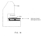
- a solid-state light device 46 capable of curing the coatings on work object 48, such as a CD/DVD storage medium, with a hermetically sealed, air cooled, LED chip array.
- device 46 may provide a power output density of about 30 to about 200 mW/cm 2 of light of a wavelength of between about 300 nm to about 400 nm.
- Device 46 includes a substrate 50 made of any material as discussed above but is preferably made of a ceramic or alumina.
- An array of LED chips 52 is disposed on substrate 50 so as to produce a light pattern slightly larger than work object 48. This larger pattern ensures proper edge cure down the sides of work object 48.
- Substrate 50 may be enclosed or mounted within a module housing 54.
- a bonding agent 56 may be used to mount substrate 50 in housing 54.
- Bonding agent 54 may be selected from known commercially available adhesives.
- bonding agent 54 has heat conductive properties.
- Housing 54 may be made of a metal that is easy to machine and is an excellent thermal conductor for heat dissipation.
- a window 58 of glass or plastic is formed in module housing 54 to allow light produced by LED chips 52 to pass through to work object 48. Window 58 is sealed to module housing 54 by a high light transmission environmental seal 60, which may be any commercially available bonding seal.
- a terminal 62 is attached to or formed on substrate 50 and is connected to a power supply 64 through a stress relief electric connection 66 mounted in an electrical insulator 68 in module housing 54.
- An optional temperature sensor 70 is also provided on substrate 50 and is connected through a terminal 72 and insulator 74 to a temperature sensor read circuit 76. Temperature sensor read circuit 76 is connected to power supply 64 to prevent LED chips 52 from overheating.
- Module housing 54 may be mounted by any connector, such as screws (not shown) on a heat sink 80.
- Heat sink 80 may have a plurality of fins made of any thermally conductive material, such as aluminum.
- a fan 82 may be connected to heat sink 80 so that fan 82 takes in ambient air and blows it through heat sink 80. Heated air is then transported away from module 46.
- LED chips 52 preferably produce light output in a range corresponding to that which activates a curing agent in the curing application of intended use. LED chips 52 may be pulsed to increase their output intensity to achieve a power output density of greater than about 400 mW/cm 2 for a particular curing application. However, other curing applications may require other light wavelengths and other power density outputs.
- Figures 4-6 show an embodiment that incorporates multiple solid-state light modules into a light bar 84 for in-line material transformation applications, such as high-intensity surface modification such as ink or coating curing or image exposure applications.
- Low Viscosity Ultraviolet Curing Ink manufactured by International Ink Co. of Gainsville, Georgia, USA, reacts at around 200mW/cm 2 using a wavelength of between about 350 nm to about 400nm.
- Light bar 84 includes multiple modules arranged in a line or an array and extends along an axis X.
- Light bar 84 is preferably moved relative to a target or work object along an axis Y allowing light output 88 to perform a process on work object 86.
- light bar 84 may be mounted on a support for moving light bar 84 over the work object.
- Light uniformity is improved by moving light bar 84 relative to work object 86 because the movement spread light output 88 evenly across work object 86 along the Y-axis.
- light bar 84 may also be moved along the X-axis to spread light output 86 along that axis.
- Light output 88 may be averaged by moving light bar 84 along both the X and Y axes, such as by vibration.
- a light averaging optical element such as a diffuser (not shown), may be incorporated in light bar 84.
- solid-state light modules may be angled so that the witness line of their joining is not evident in work object 86.
- Light bar 84 may be of various configurations and can be moved by any motive means necessary to achieve the objectives of the process for which it is to be used.
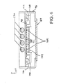
- light bar 84 includes one or more solid-state light modules 90 mounted or otherwise disposed thereon.
- Each module 90 includes a dense array of LED chips 92 mounted or otherwise disposed on a substrate 94.
- LED chips 92 may be surface mounted and wire bonded to substrate 90 in a high-density array according to the power density output of the operation.
- Each substrate 94 is preferably a printed circuit board with optimum heat transfer materials, as described above.
- Substrates 94 may be mounted to a light bar housing 96 through a bonding agent 98, preferably having good thermal conductivity.
- Modules 90 are mounted in a manner so that light output 88 produced by LED chips 92 is directed toward work object 86 through a window 89.
- a power supply 100 ( Fig.
- Each substrate 94 may include a temperature sensor 104.
- Power supply 100 senses the temperature of each substrate 94 through a second set of cables 106.
- the first and second cable sets 102 and 106 are shown simplified.
- each module 90 will have its own set of power cables so that each module 90 can be controlled separately.
- Each temperature sensor 104 is connected to a temperature sensing circuit 108 connected to power supply 100.
- a power-in bus bar 110 and a power-out bus bar 112 serve as the power input and output connections for light bar 84.
- a fluid circulation channel or conduit 114 may be used to circulate fluid around areas of the light bar requiring cooling.
- Light bar housing 96 includes upper and lower metal plates 116 and 118, such as aluminum or copper, between which fluid circulation channel or conduit 114 is positioned so that heat is transferred from light bar housing 96 to the fluid which is then carried out of light bar housing 96.
- light bar housing 96 may be provided with plural channels 120 ( Fig. 6 ) through which coolant is supplied by a first conduit (not shown) so that the coolant is in direct contact with light bar housing 96 and flows out of light bar housing 96 through a second conduit (not shown). This allows for turbulent flow of the coolant, providing greater heat transfer.
- Power supply 101 Fig.
- Light bar 84 is preferably a closed assembly to protect modules 90 from environmental damage, which might result from physical impact or contaminants, either in gas or liquid phase.
- a rigid cover 122 provides structural strength and holds window 89 which may be coated for improved UV light transmission, if desired.
- at least one optical element 124 may be provided adjacent to or otherwise associated with LED chips 92 to align light output 88 to the Z axis.
- Optical element 124 may be single or multiple elements and may be separated for each LED chip 92 or be designed to work for several or many LED chips 92.
- Other material transformation processes within the contemplation of the present invention may include resist exposure for circuit boards that include at least one material that reacts to light wavelengths between about 350 nm to about 425 nm, with an often suitable wavelength being 365 nm at a power density output of greater than 100 mW/cm 2 .
- the substrate may be ceramic or Aluminum Nitride (A1N) using a fluid cooled heat sink.
- a collimating optic micro array may be utilized to collimate light output.
- the LED chips, such as those manufactured by Cree, Inc. as discussed above, may be either be pulsed or driven continuously to obtain a power output density of greater than about 700 mW/cm 2 .
- light wavelengths of between about 300 nm to about 400 nm may be used, as various organic materials can be removed using such a range of wavelengths.
- fingerprint resides may be removed from a semiconductor wafer using a wavelength of about 365 nm and pulsing the LED chips at less than about 100 nsec pulses to obtain a power output density of greater than about 5,000 mW/cm 2 .
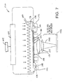
- Figure 7 shows a solid-state light device 130 wherein optical multiplication of the intensity of the light source is achieved for applications such as semiconductor wafer inspection or fluorescent inspection where a higher intensity of a single wavelength is required.
- a dense array of LED chips 132 are surface mounted on a substrate 134 having good heat transfer properties as discussed above. LED chips that produce a wavelength capable of performing an inspection process when constructed in an array providing a power density output of greater than about 50 mW/cm 2 are commercially available. One skilled in the art may select a LED chip depending on its wavelength output for a specific inspection application.
- Substrate 134 is mounted to a heat sink 136 through a bonding agent 13 8.
- Temperature sensors 140 may be provided on substrate 134 and are connected to temperature sensor circuits 142 and are connected to a computer controlled power supply 144 for operation, as discussed above.
- Power supply 144 is controlled by a computer controller 145 with thermal sensing circuitry and is connected to substrate 134 through power-in bus bar 146 and power-out bus bar 148.
- Heat sink 136 can be any possible configuration to effectively remove heat and is shown with a plurality of fins 154 to dissipate heat. Either ambient air or air-flow provided by a fan (not shown) flows over heat sink fins 154 to cool device 130.
- Optical elements 150 and 152 may be provided between LED chips 132 and a work object 156 to focus light 158 to obtain the desired intensity required for the application. For example, optical elements 150 and 152 may increase the light intensity up to between 5 and 10 times. Optical elements 150 and 152 may be any known focusing lens or intensifying optic.
- Power supply 144 can provide a variety of power waveforms, as seen in Fig. 8 , for different applications.
- power supply 144 may supply constant voltage continuously at various current levels (amps) as seen in the graphical illustrations labeled 1.1 and 1.2 for applications, such as backside wafer inspection and resist exposure for circuit boards.
- Power supply 144 can also provide pulsed power waveforms using various time on and off periods represented at C, D, E, and F, and/or current levels (amps) as seen in graphical illustrations labeled 2.1 and 2.2 for applications, such as fluorescent inspection, curing or coating for CD ROMS, and cleaning.
- current levels as seen in Fig.
- LED chips 132 may be pulsed at various frequencies for pulse times as low as 50 nsecs in order to accomplish a specific function.
- solid-state light devices like LEDs can be super pulsed, for example at currents 3 to 5 times their nominal current for short periods to achieve a higher intensity. Pulse ramp shapes allow more reliability by not overly stressing the solid-state light devices beyond what the application requires. Additionally, for material transformations where the physical process takes a period of time, the duration of the pulse can be matched to the process requirements.
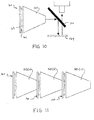
- Figure 10 illustrates another embodiment of a high-intensity light source that utilizes a reflective/transmissive optical element for inspection applications requiring power density output on greater than 50 mW/cm 2 .
- Light from a module 160 is condensed with a first optical element 162, such as a fused taper, telescopic lens pair, or other optical elements.
- Module 160 includes a dense array of LED chips 161 surface mounted on a substrate 163.
- Light is then directed to a work object 164 through a second optical element 166 such as a reflective surface.
- module 160 preferably produces light having a wavelength of between about 300nm to about 400nm.
- Second optical element 166 is preferably a highly reflective mirror that reflects greater than 95% at the light wavelength of about 380 nm and highly transmissive at the fluorescent wavelengths between 450-600 nm. Fluorescent wavelengths from work object 164 are transmitted through second optical element 166 to a camera 168 that detects the fluorescent wavelengths.
- the simplified optics and higher density light output of this embodiment enables applications not possible with prior art inspections devices due to their complicated design and limited uniformity and power density.
- the embodiments of Figs. 10 and 11 provide increased light intensity to perform, for example cleaning, sterilization, and other high power density applications.
- power density could be increased 100 times, ignoring optical losses.
- diode lasers devices in an array could be used instead.
- module 160 For backside inspection of silicon wafers or for micro electromechanical systems (MEMs) seal inspections, module 160 preferably includes LED chips or laser diodes outputting light a about 1050 nm to about 2500 nm having a combined output power density greater than 50 mW/cm 2 .
- Second optical element 166 is preferably a 50% beam splitter at the same wavelength as the light output from module 160, which is typically between 1100-1300 nm. This arrangement is effective for work objects 164 that are transmissive at 1100-1300 nm so that the wavelengths transmitted from work object 164 are propagated through second optical element 166 to camera 168 that is sensitive in the near infrared at the source wavelength.
- Light output may be further extended by stacking modules 160 as seen in Fig. 11 in series or optically in parallel.
- 80% efficiency may be achieved by surface mounting 1,000 1.8 mW LED chips at 1200 nm on substrate 163 in module 162(a); surface mounting 800 similar LED chips of substrate 163 of modules 162(b) and 162(c).
- This provides a potential of 1.44W with one module, 2.59W with two modules, and 3.7W with three modules.
- Figure 12 illustrates a power supply capable of achieving the pulsing and control requirements of the present invention.
- the programmable power supply shown herein is controlled from a general-purpose instrument bus (GPIB) interface circuit board where the output voltage and output current can be remotely programmed and monitored from a computer.
- the power supply can also be programmed to provide arbitrary output voltage and output current waveforms at various pulse repetition rates and duty cycles sufficient to achieve the functionality detailed in the embodiments.
- GPS general-purpose instrument bus
- Figures 13a and 13b show an embodiment of the present invention that allows spectral mixing by having individually addressable light emitters of predetermined colors.
- the emitters can be red, green, and/or blue.
- the emitters can be arranged in color triads.
- LED chips may be adapted to produce other colors by using color-specific phosphors or fluorescing coatings or fillers. Examples of such fillers are described in U.S. Patent No. 6,459,919 , which is incorporated herein by reference.
- each LED in earlier described embodiments may be replaced with three LEDs.
- one white LED may be replaced with three LEDs of different colors, R,G, B (Red, Green, Blue) with each separate LED having separate power coming in so that the drive circuitry would allow them to be pulsed as separate colors.
- R,G, B Red, Green, Blue
- White-light LEDs using phosphor coatings are commercially available.
- a solid-state light module 170 is partially seen in Fig. 13 in which a substrate 172 includes an array of R, G, B LED chips 174 mounted thereon having a high spatial power density so that the resulting illumination is sufficiently intense and uniform to achieve the required projection brightness. Projection applications contemplated by this invention typically would require a very dense arrangement of LED chips, such as about 237 LED chips/cm 2 . Such high density can be achieved by making substrate 172 a multilayer printed circuit board that brings the R, G, B interconnects together. Substrate 172 may include at least one temperature sensor 176 that operates to control temperature as discussed above. Module 170 is similar to module 20 described in Fig.
- Module 170 is preferably mounted on an air cooled heat sink (not shown here) similar to that described in Fig. 3 and includes drive circuitry that produces light intensity and spatial light distribution required for projection applications, such as desktop projectors. Furthermore, the R, G, B LED chips 174 and/or any optics may be controlled to allow single device control.
- Figure 13b shows the addition of an optical element 178 provided adjacent to LED chips 174 to achieve color through intensity.
- Optical element 178 may include phosphors of different colors. The each phosphor may react to a specific light intensity or a range of light intensities so that different colors may be provided by varying the light intensity of the LED array. Thus, a single wavelength light produced by the LED array may produce multiple wavelengths of light depending on the intensity of LED light output 179 intensity so that two, three, or more different wavelengths or colors can be obtained from optical element 178.
- each LED chip 174 may be individually intensity controlled; however, individual control of each LED chip 174 is not required.
- Light output may be R, G, B, and light conversion may or may not be by phosphor layers on optical element 178.
- Figure 14 shows methods of balancing and controlling the light intensity variations across the LED array. This feature may be added (if required) to all embodiments described herein.
- Light output of LED or series of LEDs are controlled by varying line resistance of DC current flow. Control of current flow will control LED light output intensity. Varying intensity provides the ability to balance light intensity evenly over an LED array. Varying intensity allows control over the LED array light output to achieve non-uniform light intensity.
- LEDs 180 are arranged in a series with a laser trim resistor 182 anywhere in the series.
- the circuit current carrying ability inside the LED array is varied. This may be achieved by varying the size of the wire bonding the LEDs 180 to the substrate.
- Wire is available in varying diameter (for example 0.001 in., 0.002 in., and 0.003 in gold wire). Resistance of the power circuit may be controlled by varying the printed circuit board trace width and/or plated thickness. Additionally, different LEDs can have different traces as needed to control current flow. Alternatively, the LEDs can be controlled using a programmable current source implemented as a transistor-based circuit to balance the current among arrays of LEDs connected in series, and/or to arrays of LEDs arranged in rows and columns. The current source may also be implemented as a programmable current output power supply.
- Figure 15 shows one possible embodiment of the present invention for projection lithography
- a module 190 projects an image on a mask or liquid crystal display 192 onto a photopolymer work object 194 forming a positive or negative image of the mask in the cured photopolymer.
- Liquid crystal display 192 may be connected to a power source (not shown) in a manner shown and described with reference to Figs. 4-6 .
- Projection lithography requires a very uniform light source.
- Module 190 includes a substrate 196 with a dense array of LED chips 198 and an air-cooled heat sink 200 as discussed above. LED chips that produce a wavelength capable of performing a projection process at a power density output of greater than 50 mW/cm 2 are commercially available.
- a collimation optic element 202 may be provided to collimate light output from the LED array and either a reducing optic 204 or an enlarging optic 206 is provided depending on the size of the image to be projected.
- FIG 16 shows one possible embodiment of the present invention for cleaning and surface modification where the maximum semiconductor light intensity is further magnified by both optical magnification and pulsing techniques to achieve power densities sufficient for ablation, material or molecular disassociation, and other effects.
- a module 208 includes a substrate 210 with a dense array of LED chips 212 having a power supply similar to that discussed with reference to Figs. 4-6 .
- a single or multiple lens 214 is provided to achieve linear magnification of light output 212 from module 208 to perform an operation on a work object 216.
- the lighting module of the present invention may be utilized in a variety of applications that require high-intensity ultraviolet light.
- the lighting module may be used in fluorescence applications for mineral, polymer, and medical inspection and measurement by using a power output density of between about 10 to about 20 mW/cm 2 of light of a wavelength of less than about 400 nm applied for at least a duration of about 40 msec.
- a power output density of between about 2 to about 42 mW/cm 2 of light of a wavelength of about 254 nm may be provided and for sterilization of blood or other biological material, a power output density of about 80 mW/cm 2 of light of a wavelength of between about 325 nm to about 390 nm may be provided.
- a power output density of between about 25 to about 300 mW/cm 2 of light of wavelengths of about 246 nm, 365 nm, 405 nm, and 436 nm is provided for a duration of between about 6 to about 30 seconds.
- a power output density of greater than about 10mJ/cm 2 of light of wavelengths between about 325 nm to about 355 nm is provided for a duration of about 20 nsec.
- a power output density of about 1 E7 W/cm 2 of light of a wavelength less than about 400 nm is utilized for a duration of about 20 nsec.
- the light might be pulsed by drive circuits and optical elements may provide an improvement of directionality and uniformity, perhaps with gradient index planar lens materials.
- the module may be used to drive fluorescing material to generate the required R, G, B output.
- three phosphors may be used as a target and one or more phosphors may be activated depending on the intensity of the light output.
- This application may be used to create visual interest or for small televisions.
- the present invention also contemplates embodiments of the invention for deformable mirror device (DMD) and LCD based projection devices, which would overcome the problem of light output balancing from R, G, B LEDs.
- DMD deformable mirror device
- LCD LCD based projection devices
- water treatments including splitting, disinfecting, ionizing, and reduction of pollutants; polymerization of medical coatings, conductive inks, controlled release drugs, and furniture coating; sterilization of medical devices, blood products, medicines, and airborne particulates; diagnostic and therapeutic uses of light for dental, skin treatment for a variety of diseases, mental disorders, and identifying particular materials through spectrographic or chromatography methods; agricultural uses including stimulating plant growth or preparing plant transitions from artificial to natural sunlight; environmental applications including the degradation of materials to accelerate biodegradation.
- spectral purity, and/or directionality of light could be achieved by including anti-reflective coated side enclosures for each LED or diode to avoid side reflections and interference effect. This will effectively prevent creative and/or destructive interferences from up-close.
- the modules can be enclosed in a series of reflectors to dramatically increase the distance to the work surface to ensure greater spectral purity.
- micro lenses could be fabricated on the LED pitch spacing to improve collimation. Such lenses might be, for example gradient index diffractive optics or Fresnel lenses.
- distributed Bragg Reflectors formed by dielectric coatings could form a resonant cavity, which would improve light directionality.
- a planar collimator such as an assembly of one or more stacked laminated transparent materials of varying index of refraction formed in any combination, or a gradient index modified glass, perhaps assembled on the LED pitch spacing.
- a power source may be constructed and arranged as seen in Fig. 17 wherein each line of LEDs in an array is powered from a separate programming source for sequencing or to vary the power to each line.
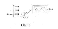
- the power density output of the modules can be tested using a machine vision inspection technique, as seen in Figs. 18 and 19 , where the individual intensity of each light module is measured. This is accomplished by placing a module 218 under an inspection camera 220 such as that shown and described in published U.S. Application US2002/0053589, filed October 2, 2001 , incorporated herein by reference.
- the camera aperture A ( Fig. 19 ) is set so that light output of the module results in pixel gray scale values less than 255.
- the location and region of interest of each individual solid-state light emitter is defined and the intensity of each solid-state light emitter is measured.
- the output intensity of all of the solid-state light emitters are digitally imaged and algorithms are used to measure overall output performance of each module to identify any elements that are not working.
- Camera 220 measures light balancing, light distribution, and overall intensity of each module.
- power density used herein is in mW/cm2. Power density may be measured at the work surface or at the exit of the light source and is typically measured through optical elements.
- An average power meter 222 with an appropriately sensitive detector at the wavelength of the light source is set up with the camera aperture opening so that the light output from the source is larger in area than the diameter of the aperture. The total average power into meter 222 within the aperture opening is recorded on meter 222.
- the optical power density for any area of the LED array is then the ratio of the measured power on the meter in mW and area of detector in cm 2 .
- the intensity of each light source in an array may be measured and the total illumination of the array is simultaneously measured so that the relative intensity of each light source relative to the overall intensity of the array is verified.
Landscapes
- Health & Medical Sciences (AREA)
- Engineering & Computer Science (AREA)
- Life Sciences & Earth Sciences (AREA)
- General Health & Medical Sciences (AREA)
- General Engineering & Computer Science (AREA)
- Veterinary Medicine (AREA)
- Public Health (AREA)
- Animal Behavior & Ethology (AREA)
- Epidemiology (AREA)
- Physics & Mathematics (AREA)
- General Physics & Mathematics (AREA)
- Chemical & Material Sciences (AREA)
- Microelectronics & Electronic Packaging (AREA)
- Optics & Photonics (AREA)
- Immunology (AREA)
- Biochemistry (AREA)
- Analytical Chemistry (AREA)
- Pathology (AREA)
- Toxicology (AREA)
- Hydrology & Water Resources (AREA)
- Environmental & Geological Engineering (AREA)
- Water Supply & Treatment (AREA)
- Organic Chemistry (AREA)
- Led Device Packages (AREA)
- Testing Or Measuring Of Semiconductors Or The Like (AREA)
- Luminescent Compositions (AREA)
- Semiconductor Lasers (AREA)
- Biomedical Technology (AREA)
- Medicinal Chemistry (AREA)
- Molecular Biology (AREA)
- Analysing Materials By The Use Of Radiation (AREA)
- Investigating, Analyzing Materials By Fluorescence Or Luminescence (AREA)
Applications Claiming Priority (2)
| Application Number | Priority Date | Filing Date | Title |
|---|---|---|---|
| US37901902P | 2002-05-08 | 2002-05-08 | |
| EP03724539A EP1508157B1 (de) | 2002-05-08 | 2003-05-08 | Hocheffiziente halbleiter-lichtquelle sowie verfahren zu deren verwendung und herstellung |
Related Parent Applications (2)
| Application Number | Title | Priority Date | Filing Date |
|---|---|---|---|
| EP03724539A Division EP1508157B1 (de) | 2002-05-08 | 2003-05-08 | Hocheffiziente halbleiter-lichtquelle sowie verfahren zu deren verwendung und herstellung |
| EP03724539.6 Division | 2003-05-08 |
Publications (4)
| Publication Number | Publication Date |
|---|---|
| EP2009676A2 true EP2009676A2 (de) | 2008-12-31 |
| EP2009676A3 EP2009676A3 (de) | 2011-06-29 |
| EP2009676B1 EP2009676B1 (de) | 2012-10-17 |
| EP2009676B8 EP2009676B8 (de) | 2012-11-21 |
Family
ID=29420475
Family Applications (2)
| Application Number | Title | Priority Date | Filing Date |
|---|---|---|---|
| EP08161355A Expired - Lifetime EP2009676B8 (de) | 2002-05-08 | 2003-05-08 | Halbleitermaterial-Prüfsystem |
| EP03724539A Revoked EP1508157B1 (de) | 2002-05-08 | 2003-05-08 | Hocheffiziente halbleiter-lichtquelle sowie verfahren zu deren verwendung und herstellung |
Family Applications After (1)
| Application Number | Title | Priority Date | Filing Date |
|---|---|---|---|
| EP03724539A Revoked EP1508157B1 (de) | 2002-05-08 | 2003-05-08 | Hocheffiziente halbleiter-lichtquelle sowie verfahren zu deren verwendung und herstellung |
Country Status (10)
| Country | Link |
|---|---|
| US (3) | US8192053B2 (de) |
| EP (2) | EP2009676B8 (de) |
| JP (1) | JP2005524989A (de) |
| KR (1) | KR20050044865A (de) |
| CN (1) | CN1653297B (de) |
| AT (1) | ATE535009T1 (de) |
| AU (1) | AU2003235489A1 (de) |
| ES (1) | ES2378067T3 (de) |
| TW (1) | TWI229946B (de) |
| WO (1) | WO2003096387A2 (de) |
Cited By (3)
| Publication number | Priority date | Publication date | Assignee | Title |
|---|---|---|---|---|
| DE102009004117A1 (de) * | 2009-01-08 | 2010-07-15 | Osram Gesellschaft mit beschränkter Haftung | Projektionsmodul |
| FR2968097A1 (fr) * | 2010-11-30 | 2012-06-01 | Altix | Machine d'exposition de panneaux. |
| CN115235030A (zh) * | 2021-04-23 | 2022-10-25 | 重庆美的制冷设备有限公司 | 一种空气处理装置及空气处理方法 |
Families Citing this family (375)
| Publication number | Priority date | Publication date | Assignee | Title |
|---|---|---|---|---|
| GB2329756A (en) | 1997-09-25 | 1999-03-31 | Univ Bristol | Assemblies of light emitting diodes |
| ATE535009T1 (de) | 2002-05-08 | 2011-12-15 | Phoseon Technology Inc | Hocheffiziente halbleiter-lichtquelle sowie verfahren zu deren verwendung und herstellung |
| US20060293727A1 (en) * | 2002-05-09 | 2006-12-28 | Greg Spooner | System and method for treating exposed tissue with light emitting diodes |
| EP1551329A4 (de) | 2002-07-25 | 2006-08-16 | Jonathan S Dahm | Verfahren und vorrichtung zur verwendung von leuchtdioden zum aushärten |
| AU2003298561A1 (en) | 2002-08-23 | 2004-05-13 | Jonathan S. Dahm | Method and apparatus for using light emitting diodes |
| US7775685B2 (en) * | 2003-05-27 | 2010-08-17 | Cree, Inc. | Power surface mount light emitting die package |
| US7244965B2 (en) * | 2002-09-04 | 2007-07-17 | Cree Inc, | Power surface mount light emitting die package |
| WO2004051705A2 (en) | 2002-12-02 | 2004-06-17 | 3M Innovative Properties Company | Illumination system using a plurality of light sources |
| US7671346B2 (en) * | 2003-01-09 | 2010-03-02 | Con-Trol-Cure, Inc. | Light emitting apparatus and method for curing inks, coatings and adhesives |
| US20040164325A1 (en) * | 2003-01-09 | 2004-08-26 | Con-Trol-Cure, Inc. | UV curing for ink jet printer |
| US7465909B2 (en) | 2003-01-09 | 2008-12-16 | Con-Trol-Cure, Inc. | UV LED control loop and controller for causing emitting UV light at a much greater intensity for UV curing |
| US7498065B2 (en) * | 2003-01-09 | 2009-03-03 | Con-Trol-Cure, Inc. | UV printing and curing of CDs, DVDs, Golf Balls And Other Products |
| US7211299B2 (en) * | 2003-01-09 | 2007-05-01 | Con-Trol-Cure, Inc. | UV curing method and apparatus |
| US7399982B2 (en) * | 2003-01-09 | 2008-07-15 | Con-Trol-Cure, Inc | UV curing system and process with increased light intensity |
| US7175712B2 (en) * | 2003-01-09 | 2007-02-13 | Con-Trol-Cure, Inc. | Light emitting apparatus and method for curing inks, coatings and adhesives |
| US7137696B2 (en) * | 2003-01-09 | 2006-11-21 | Con-Trol-Cure, Inc. | Ink jet UV curing |
| US20060204670A1 (en) * | 2003-01-09 | 2006-09-14 | Con-Trol-Cure, Inc. | UV curing method and apparatus |
| US20060121208A1 (en) * | 2003-01-09 | 2006-06-08 | Siegel Stephen B | Multiple wavelength UV curing |
| KR20060009021A (ko) * | 2003-06-04 | 2006-01-27 | 가부시키가이샤 미마키 엔지니어링 | Uv 잉크를 사용하는 잉크젯 프린터 |
| JP2005175039A (ja) * | 2003-12-09 | 2005-06-30 | Kenichiro Miyahara | 発光素子搭載用基板及び発光素子 |
| JP4200849B2 (ja) * | 2003-07-17 | 2008-12-24 | 日産自動車株式会社 | 車両用赤外線投光器 |
| KR20050015152A (ko) * | 2003-08-04 | 2005-02-21 | 삼성전자주식회사 | 프로젝터 |
| CA2938411C (en) | 2003-09-12 | 2019-03-05 | Minnow Medical, Llc | Selectable eccentric remodeling and/or ablation of atherosclerotic material |
| EP1678442B8 (de) * | 2003-10-31 | 2013-06-26 | Phoseon Technology, Inc. | LED-Lichtmodul und Herstellungsverfahren |
| WO2005043954A2 (en) * | 2003-10-31 | 2005-05-12 | Phoseon Technology, Inc. | Series wiring of highly reliable light sources |
| US7250611B2 (en) | 2003-12-02 | 2007-07-31 | 3M Innovative Properties Company | LED curing apparatus and method |
| US7403680B2 (en) | 2003-12-02 | 2008-07-22 | 3M Innovative Properties Company | Reflective light coupler |
| US7329887B2 (en) | 2003-12-02 | 2008-02-12 | 3M Innovative Properties Company | Solid state light device |
| US7456805B2 (en) | 2003-12-18 | 2008-11-25 | 3M Innovative Properties Company | Display including a solid state light device and method using same |
| US20050257912A1 (en) * | 2004-01-12 | 2005-11-24 | Litelaser Llc | Laser cooling system and method |
| TWI257718B (en) | 2004-03-18 | 2006-07-01 | Phoseon Technology Inc | Direct cooling of LEDs |
| WO2005091392A1 (en) | 2004-03-18 | 2005-09-29 | Phoseon Technology, Inc. | Micro-reflectors on a substrate for high-density led array |
| US7128421B2 (en) * | 2004-03-29 | 2006-10-31 | Infocus Corporation | Thermal management of projection apparatus |
| EP1743384B1 (de) | 2004-03-30 | 2015-08-05 | Phoseon Technology, Inc. | Led-gruppe mit led-detektoren auf gruppenbasis |
| DK1756876T3 (da) * | 2004-04-12 | 2011-07-18 | Phoseon Technology Inc | LED-opstilling med høj densitet |
| WO2005100961A2 (en) | 2004-04-19 | 2005-10-27 | Phoseon Technology, Inc. | Imaging semiconductor strucutures using solid state illumination |
| GB2413840B (en) * | 2004-05-07 | 2006-06-14 | Savage Marine Ltd | Underwater lighting |
| US7252385B2 (en) * | 2004-05-11 | 2007-08-07 | Infocus Corporation | Projection LED cooling |
| CN100594327C (zh) | 2004-06-15 | 2010-03-17 | 汉高公司 | 大功率led电-光学器件组件 |
| JP2006041406A (ja) * | 2004-07-30 | 2006-02-09 | Matsushita Electric Ind Co Ltd | レーザ加熱設備 |
| US9713730B2 (en) | 2004-09-10 | 2017-07-25 | Boston Scientific Scimed, Inc. | Apparatus and method for treatment of in-stent restenosis |
| US8396548B2 (en) | 2008-11-14 | 2013-03-12 | Vessix Vascular, Inc. | Selective drug delivery in a lumen |
| TWI257992B (en) * | 2004-09-13 | 2006-07-11 | Neobulb Technologies Inc | Lighting device with highly efficient heat dissipation structure |
| US7220040B2 (en) * | 2004-11-12 | 2007-05-22 | Harris Corporation | LED light engine for backlighting a liquid crystal display |
| US20060126346A1 (en) * | 2004-12-10 | 2006-06-15 | Paul R. Mighetto | Apparatus for providing light |
| US7387403B2 (en) * | 2004-12-10 | 2008-06-17 | Paul R. Mighetto | Modular lighting apparatus |
| US8686277B2 (en) * | 2004-12-27 | 2014-04-01 | Intel Corporation | Microelectronic assembly including built-in thermoelectric cooler and method of fabricating same |
| KR101288758B1 (ko) | 2004-12-30 | 2013-07-23 | 포세온 테크날러지 인코퍼레이티드 | 산업 공정에서 광원을 사용하는 시스템 및 방법 |
| US7394479B2 (en) * | 2005-03-02 | 2008-07-01 | Marken Corporation | Pulsed laser printing |
| US8748923B2 (en) * | 2005-03-14 | 2014-06-10 | Philips Lumileds Lighting Company Llc | Wavelength-converted semiconductor light emitting device |
| US7341878B2 (en) * | 2005-03-14 | 2008-03-11 | Philips Lumileds Lighting Company, Llc | Wavelength-converted semiconductor light emitting device |
| JP5080009B2 (ja) * | 2005-03-22 | 2012-11-21 | 日立ビアメカニクス株式会社 | 露光方法 |
| JP4410134B2 (ja) * | 2005-03-24 | 2010-02-03 | 日立ビアメカニクス株式会社 | パターン露光方法及び装置 |
| JP2006310402A (ja) * | 2005-04-26 | 2006-11-09 | Sony Corp | 光源基板製造方法、光源基板、バックライト装置、液晶ディスプレイ装置、調整装置 |
| KR101240999B1 (ko) | 2005-04-27 | 2013-03-08 | 코닌클리즈케 필립스 일렉트로닉스 엔.브이. | 발광 반도체 장치용 냉각 장치 및 그러한 냉각 장치의 제조방법 |
| US8459852B2 (en) | 2007-10-05 | 2013-06-11 | Dental Equipment, Llc | LED-based dental exam lamp |
| JP2006314686A (ja) * | 2005-05-16 | 2006-11-24 | Olympus Medical Systems Corp | 内視鏡 |
| DE102005026662A1 (de) * | 2005-05-31 | 2006-12-07 | Karl Storz Gmbh & Co. Kg | Lichtquelle für die Endoskopie oder Mikroskopie |
| WO2006128317A1 (de) * | 2005-06-03 | 2006-12-07 | Elpatronic Ag | Verfahren zur beleuchtung und beleuchtungsanordnung |
| US7980743B2 (en) * | 2005-06-14 | 2011-07-19 | Cree, Inc. | LED backlighting for displays |
| JP4771402B2 (ja) * | 2005-06-29 | 2011-09-14 | 国立大学法人徳島大学 | 紫外線殺菌装置 |
| KR100671545B1 (ko) * | 2005-07-01 | 2007-01-19 | 삼성전자주식회사 | Led 어레이 모듈 |
| DE102005031792A1 (de) * | 2005-07-07 | 2007-01-11 | Carl Zeiss Smt Ag | Verfahren zur Entfernung von Kontamination von optischen Elementen, insbesondere von Oberflächen optischer Elemente sowie ein optisches System oder Teilsystem hierfür |
| JP4581946B2 (ja) * | 2005-09-29 | 2010-11-17 | セイコーエプソン株式会社 | 画像表示装置 |
| US7479660B2 (en) | 2005-10-21 | 2009-01-20 | Perkinelmer Elcos Gmbh | Multichip on-board LED illumination device |
| CN101313172A (zh) * | 2005-11-22 | 2008-11-26 | 皇家飞利浦电子股份有限公司 | 发光模块和制造方法 |
| DE102005061204A1 (de) * | 2005-12-21 | 2007-07-05 | Perkinelmer Elcos Gmbh | Beleuchtungsvorrichtung, Beleuchtungssteuergerät und Beleuchtungssystem |
| US7642527B2 (en) * | 2005-12-30 | 2010-01-05 | Phoseon Technology, Inc. | Multi-attribute light effects for use in curing and other applications involving photoreactions and processing |
| US20070217199A1 (en) * | 2006-03-17 | 2007-09-20 | Light Dimensions, Inc. | Light-based dermal enhancing apparatus and methods of use |
| GB0606604D0 (en) * | 2006-04-01 | 2006-05-10 | P W Circuts Ltd | Treatment apparatus |
| DE102006015335B4 (de) * | 2006-04-03 | 2013-05-02 | Ivoclar Vivadent Ag | Halbleiter-Strahlungsquelle sowie Lichthärtgerät |
| US8019435B2 (en) | 2006-05-02 | 2011-09-13 | Boston Scientific Scimed, Inc. | Control of arterial smooth muscle tone |
| US8596819B2 (en) | 2006-05-31 | 2013-12-03 | Cree, Inc. | Lighting device and method of lighting |
| USD585997S1 (en) | 2006-10-13 | 2009-02-03 | Light Dimensions, Inc. | Light-based dermal enhancing apparatus |
| EP2992850A1 (de) | 2006-10-18 | 2016-03-09 | Vessix Vascular, Inc. | Herbeiführung gewünschter temperatureffekte auf körpergewebe |
| AU2007310988B2 (en) | 2006-10-18 | 2013-08-15 | Vessix Vascular, Inc. | Tuned RF energy and electrical tissue characterization for selective treatment of target tissues |
| EP2076194B1 (de) | 2006-10-18 | 2013-04-24 | Vessix Vascular, Inc. | System zur herbeiführung gewünschter temperatureffekte in körpergewebe |
| CN102119580A (zh) * | 2006-10-31 | 2011-07-06 | 皇家飞利浦电子股份有限公司 | 发光元件光源及其温度管理系统 |
| KR100846975B1 (ko) | 2006-11-09 | 2008-07-17 | 삼성에스디아이 주식회사 | 밀봉 장치 및 그를 이용한 표시 장치의 제조 방법 |
| TWI345429B (en) | 2006-11-13 | 2011-07-11 | Polytronics Technology Corp | Light emitting diode apparatus |
| ITFI20060307A1 (it) * | 2006-12-05 | 2008-06-06 | Light 4 Tech Firenze S R L | Dispositivo basato su tecnologia led per l'emostasi di vasi sanguigni |
| GB0624453D0 (en) | 2006-12-06 | 2007-01-17 | Sun Chemical Bv | A solid state radiation source array |
| US8221671B2 (en) * | 2007-01-17 | 2012-07-17 | 3D Systems, Inc. | Imager and method for consistent repeatable alignment in a solid imaging apparatus |
| WO2008094607A1 (en) * | 2007-01-30 | 2008-08-07 | Cortron Corporation | Spectrally controlled high energy density light source photopolymer exposure system |
| US8115213B2 (en) | 2007-02-08 | 2012-02-14 | Phoseon Technology, Inc. | Semiconductor light sources, systems, and methods |
| WO2008108210A1 (ja) * | 2007-02-26 | 2008-09-12 | Rohm Co., Ltd. | 線状光源装置およびそれを備えた画像読み取り装置 |
| JP2010522333A (ja) * | 2007-03-23 | 2010-07-01 | パーティクル・メージャーリング・システムズ・インコーポレーテッド | 排出冷却式光源を備えた光学式パーティクルセンサ |
| WO2008119550A1 (en) * | 2007-04-02 | 2008-10-09 | Viscom Ag | Inspection apparatus and method |
| US8203260B2 (en) * | 2007-04-13 | 2012-06-19 | Intematix Corporation | Color temperature tunable white light source |
| WO2008125330A1 (en) * | 2007-04-16 | 2008-10-23 | Viscom Ag | Through-substrate optical imaging device and method |
| US7703943B2 (en) * | 2007-05-07 | 2010-04-27 | Intematix Corporation | Color tunable light source |
| EP1992486B1 (de) * | 2007-05-15 | 2012-10-03 | Komori Corporation | Flüssigkeitshärtungsvorrichtung für eine Flüssigkeitsübertragungsvorrichtung |
| DE102007028860A1 (de) * | 2007-06-22 | 2008-12-24 | Josef Lindthaler | Vorrichtung zur Kontaktbelichtung einer Druckschablone |
| CN101755483B (zh) * | 2007-07-23 | 2012-05-30 | 皇家飞利浦电子股份有限公司 | 发光单元装置及其控制系统和方法 |
| GB0714363D0 (en) * | 2007-07-24 | 2007-09-05 | P W Circuits Ltd | Treatment apparatus |
| EP2025220A1 (de) * | 2007-08-15 | 2009-02-18 | Lemnis Lighting Patent Holding B.V. | LED Beleuchtungsvorrichtung für Pflanzenbau |
| ATE533043T1 (de) * | 2007-08-31 | 2011-11-15 | Icos Vision Systems Nv | Vorrichtung und verfahren zum nachweis von halbleitersubstratanomalien |
| CN101377289A (zh) * | 2007-08-31 | 2009-03-04 | 富准精密工业(深圳)有限公司 | 发光二极管灯具 |
| EP2191655B8 (de) * | 2007-09-13 | 2019-01-09 | Philips Lighting Holding B.V. | Beleuchtungsvorrichtung für gepixelte darstellung |
| US20090071168A1 (en) * | 2007-09-17 | 2009-03-19 | American Environmental Systems, Inc. | Device and methods for internal cooling of an integrated circuit (IC) |
| US20090140271A1 (en) * | 2007-11-30 | 2009-06-04 | Wen-Jyh Sah | Light emitting unit |
| CN101470298B (zh) * | 2007-12-29 | 2012-01-11 | 富士迈半导体精密工业(上海)有限公司 | 背光模组 |
| TWI403259B (zh) * | 2008-02-01 | 2013-07-21 | Foxsemicon Integrated Tech Inc | 發光二極體照明裝置及其散熱方法 |
| JP2009208463A (ja) * | 2008-02-06 | 2009-09-17 | Ryobi Ltd | 印刷機の印刷方法及び印刷機 |
| DE102008038857A1 (de) * | 2008-03-31 | 2009-10-01 | Osram Opto Semiconductors Gmbh | Beleuchtungseinrichtung |
| TWI385340B (zh) * | 2008-04-03 | 2013-02-11 | Foxconn Tech Co Ltd | 發光二極體路燈 |
| DE102008018763A1 (de) * | 2008-04-14 | 2009-11-05 | Kristin Bartsch | Lithografiebelichtungseinrichtung |
| GB0809650D0 (en) * | 2008-05-29 | 2008-07-02 | Integration Technology Ltd | LED Device and arrangement |
| TW200951359A (en) * | 2008-06-06 | 2009-12-16 | Taiwan Solutions Systems Corp | LED lamp module and its fabricating method |
| CN101614386A (zh) * | 2008-06-25 | 2009-12-30 | 富准精密工业(深圳)有限公司 | 发光二极管灯具 |
| US20090322800A1 (en) * | 2008-06-25 | 2009-12-31 | Dolby Laboratories Licensing Corporation | Method and apparatus in various embodiments for hdr implementation in display devices |
| US8070324B2 (en) * | 2008-07-30 | 2011-12-06 | Mp Design Inc. | Thermal control system for a light-emitting diode fixture |
| EP2154419B1 (de) * | 2008-07-31 | 2016-07-06 | Toshiba Lighting & Technology Corporation | Lampe mit eingebautem Vorschaltgerät |
| US8525200B2 (en) * | 2008-08-18 | 2013-09-03 | Taiwan Semiconductor Manufacturing Company, Ltd. | Light-emitting diode with non-metallic reflector |
| US8183585B2 (en) * | 2008-09-16 | 2012-05-22 | Osram Sylvania Inc. | Lighting module |
| WO2010043275A1 (en) * | 2008-10-17 | 2010-04-22 | Huntsman Advanced Materials (Switzerland) Gmbh | Improvements for rapid prototyping apparatus |
| US20100098399A1 (en) * | 2008-10-17 | 2010-04-22 | Kurt Breish | High intensity, strobed led micro-strip for microfilm imaging system and methods |
| EP2355737B1 (de) | 2008-11-17 | 2021-08-11 | Boston Scientific Scimed, Inc. | Selektive akkumulation von energie ohne informationen über eine gewebetopographie |
| US8651704B1 (en) | 2008-12-05 | 2014-02-18 | Musco Corporation | Solid state light fixture with cooling system with heat rejection management |
| US20100149805A1 (en) * | 2008-12-17 | 2010-06-17 | Fridy Joseph | Led lighting laminate with integrated cooling |
| US8390193B2 (en) * | 2008-12-31 | 2013-03-05 | Intematix Corporation | Light emitting device with phosphor wavelength conversion |
| US8314408B2 (en) | 2008-12-31 | 2012-11-20 | Draka Comteq, B.V. | UVLED apparatus for curing glass-fiber coatings |
| US8678612B2 (en) * | 2009-04-14 | 2014-03-25 | Phoseon Technology, Inc. | Modular light source |
| CA2759138C (en) | 2009-04-21 | 2017-05-30 | Purill Bv | Method and device for disinfection and/or purification of a product |
| JP5345443B2 (ja) * | 2009-04-21 | 2013-11-20 | 株式会社日立ハイテクノロジーズ | 露光装置、露光光照射方法、及び表示用パネル基板の製造方法 |
| EP2773167A1 (de) * | 2009-05-14 | 2014-09-03 | 4233999 Canada, Inc. | System und Verfahren zur Ausgabe von hochauflösenden Bildern mithilfe monolithischer LED-Arrays |
| US20120196011A1 (en) * | 2009-08-07 | 2012-08-02 | Felix Perry D | Method and apparatus for surface sanitizing of food products in a cooking appliance using ultraviolet light |
| KR20110001935U (ko) * | 2009-08-19 | 2011-02-25 | 주식회사 영동테크 | 모듈화 된 엘이디 등기구의 냉각 장치 |
| FR2949533B1 (fr) * | 2009-08-28 | 2012-08-24 | Olivier Pinon | Mobilier d'eclairage electrique |
| USD632821S1 (en) | 2009-09-21 | 2011-02-15 | Glowble SSL, Inc. | LED light fixture |
| USD633632S1 (en) | 2009-09-21 | 2011-03-01 | Glowble SSL, Inc. | LED light fixture |
| US8845130B2 (en) * | 2009-12-09 | 2014-09-30 | Tyco Electronics Corporation | LED socket assembly |
| US8878454B2 (en) | 2009-12-09 | 2014-11-04 | Tyco Electronics Corporation | Solid state lighting system |
| US8210715B2 (en) * | 2009-12-09 | 2012-07-03 | Tyco Electronics Corporation | Socket assembly with a thermal management structure |
| US8235549B2 (en) * | 2009-12-09 | 2012-08-07 | Tyco Electronics Corporation | Solid state lighting assembly |
| US8241044B2 (en) * | 2009-12-09 | 2012-08-14 | Tyco Electronics Corporation | LED socket assembly |
| EP2332490B1 (de) * | 2009-12-10 | 2017-10-11 | Ivoclar Vivadent AG | Lichthärtgerät für Dentalzwecke |
| KR101663563B1 (ko) * | 2009-12-24 | 2016-10-07 | 엘지디스플레이 주식회사 | 액정표시장치의 제조방법 |
| JP5820397B2 (ja) * | 2010-01-27 | 2015-11-24 | ヘレウス ノーブルライト アメリカ エルエルシー | マイクロチャンネル冷却型高熱負荷発光装置 |
| US8809820B2 (en) | 2010-01-27 | 2014-08-19 | Heraeus Noblelight Fusion Uv Inc. | Micro-channel-cooled high heat load light emitting device |
| US9825425B2 (en) * | 2013-06-19 | 2017-11-21 | Apple Inc. | Integrated structured-light projector comprising light-emitting elements on a substrate |
| US9740019B2 (en) | 2010-02-02 | 2017-08-22 | Apple Inc. | Integrated structured-light projector |
| JP4814394B2 (ja) * | 2010-03-05 | 2011-11-16 | シャープ株式会社 | 発光装置の製造方法 |
| US9583690B2 (en) * | 2010-04-07 | 2017-02-28 | Shenzhen Qin Bo Core Technology Development Co., Ltd. | LED lampwick, LED chip, and method for manufacturing LED chip |
| KR20130108067A (ko) | 2010-04-09 | 2013-10-02 | 베식스 바스큘라 인코포레이티드 | 조직 치료를 위한 발전 및 제어 장치 |
| US20130003382A1 (en) * | 2010-04-09 | 2013-01-03 | Sharp Kabushiki Kaisha | Lighting device, plant cultivation device, and method for cooling lighting device |
| IT1399490B1 (it) * | 2010-04-09 | 2013-04-19 | Bevilacqua De | Dispositivo di illuminazione a led |
| US9192790B2 (en) | 2010-04-14 | 2015-11-24 | Boston Scientific Scimed, Inc. | Focused ultrasonic renal denervation |
| US20110069502A1 (en) * | 2010-04-14 | 2011-03-24 | David Hum | Mounting Fixture for LED Lighting Modules |
| WO2011139280A1 (en) * | 2010-05-07 | 2011-11-10 | Broan-Nutone, Llc | Range hood lighting arrangement |
| DK2388239T3 (da) | 2010-05-20 | 2017-04-24 | Draka Comteq Bv | Hærdningsapparat, der anvender vinklede UV-LED'er |
| US8871311B2 (en) | 2010-06-03 | 2014-10-28 | Draka Comteq, B.V. | Curing method employing UV sources that emit differing ranges of UV radiation |
| US8473067B2 (en) | 2010-06-11 | 2013-06-25 | Boston Scientific Scimed, Inc. | Renal denervation and stimulation employing wireless vascular energy transfer arrangement |
| US9155589B2 (en) | 2010-07-30 | 2015-10-13 | Boston Scientific Scimed, Inc. | Sequential activation RF electrode set for renal nerve ablation |
| US9408661B2 (en) | 2010-07-30 | 2016-08-09 | Patrick A. Haverkost | RF electrodes on multiple flexible wires for renal nerve ablation |
| US9084609B2 (en) | 2010-07-30 | 2015-07-21 | Boston Scientific Scime, Inc. | Spiral balloon catheter for renal nerve ablation |
| US9358365B2 (en) | 2010-07-30 | 2016-06-07 | Boston Scientific Scimed, Inc. | Precision electrode movement control for renal nerve ablation |
| US9463062B2 (en) | 2010-07-30 | 2016-10-11 | Boston Scientific Scimed, Inc. | Cooled conductive balloon RF catheter for renal nerve ablation |
| EP2418183B1 (de) | 2010-08-10 | 2018-07-25 | Draka Comteq B.V. | Verfahren zur Härtung beschichteter Glasfasern mit erhöhter UVLED-Intensität |
| MX2010009169A (es) * | 2010-08-10 | 2012-02-21 | Andres Abelino Choza Romero | Aparato para desinfectar líquidos, mediante el uso de luz ultravioleta. |
| CN102412359B (zh) * | 2010-09-21 | 2018-12-07 | 亿光电子(中国)有限公司 | 用于一微型投影系统的发光二极管装置 |
| TWM422644U (en) * | 2010-09-27 | 2012-02-11 | chong-yuan Cai | Light-emitting diode capable of dissipating heat and controlling light shape |
| US8974451B2 (en) | 2010-10-25 | 2015-03-10 | Boston Scientific Scimed, Inc. | Renal nerve ablation using conductive fluid jet and RF energy |
| US20120098434A1 (en) * | 2010-10-26 | 2012-04-26 | Wybron, Inc. | Led light assembly and associated method |
| US9220558B2 (en) | 2010-10-27 | 2015-12-29 | Boston Scientific Scimed, Inc. | RF renal denervation catheter with multiple independent electrodes |
| US9028485B2 (en) | 2010-11-15 | 2015-05-12 | Boston Scientific Scimed, Inc. | Self-expanding cooling electrode for renal nerve ablation |
| US9089350B2 (en) | 2010-11-16 | 2015-07-28 | Boston Scientific Scimed, Inc. | Renal denervation catheter with RF electrode and integral contrast dye injection arrangement |
| US9668811B2 (en) | 2010-11-16 | 2017-06-06 | Boston Scientific Scimed, Inc. | Minimally invasive access for renal nerve ablation |
| US9326751B2 (en) | 2010-11-17 | 2016-05-03 | Boston Scientific Scimed, Inc. | Catheter guidance of external energy for renal denervation |
| US9060761B2 (en) | 2010-11-18 | 2015-06-23 | Boston Scientific Scime, Inc. | Catheter-focused magnetic field induced renal nerve ablation |
| US9192435B2 (en) | 2010-11-22 | 2015-11-24 | Boston Scientific Scimed, Inc. | Renal denervation catheter with cooled RF electrode |
| US8376588B2 (en) * | 2010-11-22 | 2013-02-19 | Hsu Li Yen | Gain structure of LED tubular lamp for uniforming light and dissipating heat |
| US9023034B2 (en) | 2010-11-22 | 2015-05-05 | Boston Scientific Scimed, Inc. | Renal ablation electrode with force-activatable conduction apparatus |
| US20120157993A1 (en) | 2010-12-15 | 2012-06-21 | Jenson Mark L | Bipolar Off-Wall Electrode Device for Renal Nerve Ablation |
| WO2012085669A2 (en) | 2010-12-21 | 2012-06-28 | Derose, Anthony | Fluid cooled lighting element |
| KR101167461B1 (ko) * | 2010-12-27 | 2012-07-31 | 삼성전기주식회사 | 레이져 네비게이션 모듈 |
| JP5254308B2 (ja) * | 2010-12-27 | 2013-08-07 | 東京エレクトロン株式会社 | 液処理装置、液処理方法及びその液処理方法を実行させるためのプログラムを記録した記録媒体 |
| WO2012100095A1 (en) | 2011-01-19 | 2012-07-26 | Boston Scientific Scimed, Inc. | Guide-compatible large-electrode catheter for renal nerve ablation with reduced arterial injury |
| US8596815B2 (en) | 2011-04-15 | 2013-12-03 | Dicon Fiberoptics Inc. | Multiple wavelength LED array illuminator for fluorescence microscopy |
| US8979316B2 (en) * | 2011-05-11 | 2015-03-17 | Dicon Fiberoptics Inc. | Zoom spotlight using LED array |
| CN103813745B (zh) | 2011-07-20 | 2016-06-29 | 波士顿科学西美德公司 | 用以可视化、对准和消融神经的经皮装置及方法 |
| JP6106669B2 (ja) | 2011-07-22 | 2017-04-05 | ボストン サイエンティフィック サイムド,インコーポレイテッドBoston Scientific Scimed,Inc. | ヘリカル・ガイド内に配置可能な神経調節要素を有する神経調節システム |
| US8911117B2 (en) * | 2011-07-26 | 2014-12-16 | Mike Hulsman | LED lighting apparatus with a high efficiency convective heat sink |
| KR101970675B1 (ko) * | 2011-08-04 | 2019-04-19 | 가부시키가이샤 한도오따이 에네루기 켄큐쇼 | 발광 장치 및 조명 장치 |
| US20130032325A1 (en) * | 2011-08-05 | 2013-02-07 | Deng wei-shan | Thermostatic control led thermal module |
| US8749796B2 (en) | 2011-08-09 | 2014-06-10 | Primesense Ltd. | Projectors of structured light |
| US9429309B2 (en) | 2011-09-26 | 2016-08-30 | Ideal Industries, Inc. | Device for securing a source of LED light to a heat sink surface |
| US9249955B2 (en) | 2011-09-26 | 2016-02-02 | Ideal Industries, Inc. | Device for securing a source of LED light to a heat sink surface |
| US9423119B2 (en) | 2011-09-26 | 2016-08-23 | Ideal Industries, Inc. | Device for securing a source of LED light to a heat sink surface |
| US9186210B2 (en) | 2011-10-10 | 2015-11-17 | Boston Scientific Scimed, Inc. | Medical devices including ablation electrodes |
| US9420955B2 (en) | 2011-10-11 | 2016-08-23 | Boston Scientific Scimed, Inc. | Intravascular temperature monitoring system and method |
| EP2765940B1 (de) | 2011-10-11 | 2015-08-26 | Boston Scientific Scimed, Inc. | Wandferne elektrodenvorrichtung zur nervenmodulation |
| US9364284B2 (en) | 2011-10-12 | 2016-06-14 | Boston Scientific Scimed, Inc. | Method of making an off-wall spacer cage |
| US9115868B2 (en) | 2011-10-13 | 2015-08-25 | Intematix Corporation | Wavelength conversion component with improved protective characteristics for remote wavelength conversion |
| WO2013059202A1 (en) | 2011-10-18 | 2013-04-25 | Boston Scientific Scimed, Inc. | Integrated crossing balloon catheter |
| US9162046B2 (en) | 2011-10-18 | 2015-10-20 | Boston Scientific Scimed, Inc. | Deflectable medical devices |
| JP2013085737A (ja) * | 2011-10-19 | 2013-05-13 | Sony Corp | 医用装置、治療装置、光プローブの評価方法及び校正方法 |
| US9500340B2 (en) * | 2011-10-25 | 2016-11-22 | A-Dec, Inc. | Dental light using LEDs |
| TWI457517B (zh) * | 2011-10-26 | 2014-10-21 | Global Fiberoptics Inc | Led陣列調焦發光裝置及形成聚焦光束的方法 |
| EP2775948B1 (de) | 2011-11-08 | 2018-04-04 | Boston Scientific Scimed, Inc. | Ostiale nierennervenablation |
| US9119600B2 (en) | 2011-11-15 | 2015-09-01 | Boston Scientific Scimed, Inc. | Device and methods for renal nerve modulation monitoring |
| US9119632B2 (en) | 2011-11-21 | 2015-09-01 | Boston Scientific Scimed, Inc. | Deflectable renal nerve ablation catheter |
| WO2013078106A1 (en) | 2011-11-21 | 2013-05-30 | Nonomura Arthur M | Methods and systems for growing plants using silicate-based substrates, cultivation of enhanced photosynthetic productivity and photosafening by utilization of exogenous glycopyranosides for endogenous glycopyranosyl-protein derivatives, and formulations, processes and systems for the same |
| US9265969B2 (en) | 2011-12-21 | 2016-02-23 | Cardiac Pacemakers, Inc. | Methods for modulating cell function |
| WO2013096922A1 (en) | 2011-12-23 | 2013-06-27 | Vessix Vascular, Inc. | Methods and apparatuses for remodeling tissue of or adjacent to a body passage |
| EP2797534A1 (de) | 2011-12-28 | 2014-11-05 | Boston Scientific Scimed, Inc. | Vorrichtung und verfahren zur nervenmodulation unter verwendung eines neuartigen ablationskatheters mit polymerischen ablationselementen |
| US9050106B2 (en) | 2011-12-29 | 2015-06-09 | Boston Scientific Scimed, Inc. | Off-wall electrode device and methods for nerve modulation |
| US8568001B2 (en) | 2012-02-03 | 2013-10-29 | Tyco Electronics Corporation | LED socket assembly |
| DE102012203442B4 (de) * | 2012-03-05 | 2021-08-05 | Coretronic Corporation | Beleuchtungsvorrichtung mit einer pumplaserreihe und verfahren zum betreiben dieser beleuchtungsvorrichtung |
| JP5962103B2 (ja) * | 2012-03-21 | 2016-08-03 | カシオ計算機株式会社 | 蛍光体デバイス、照明装置及びプロジェクタ装置 |
| US10660703B2 (en) | 2012-05-08 | 2020-05-26 | Boston Scientific Scimed, Inc. | Renal nerve modulation devices |
| US9028115B1 (en) | 2012-05-11 | 2015-05-12 | Musco Corporation | Apparatus, method, and system for lighting fixture cooling |
| AU2013266917C1 (en) | 2012-05-21 | 2017-06-08 | Innovation Hammer Llc | Methods for rendering micellar coordination complexes safe for the treatment of plants and formulations for same |
| US9217561B2 (en) * | 2012-06-15 | 2015-12-22 | Lumencor, Inc. | Solid state light source for photocuring |
| TWI457890B (zh) * | 2012-08-17 | 2014-10-21 | 聚積科技股份有限公司 | Display structure and display |
| CN104540465A (zh) | 2012-08-24 | 2015-04-22 | 波士顿科学西美德公司 | 带有含单独微孔隙区域的球囊的血管内导管 |
| WO2014043687A2 (en) | 2012-09-17 | 2014-03-20 | Boston Scientific Scimed, Inc. | Self-positioning electrode system and method for renal nerve modulation |
| US10398464B2 (en) | 2012-09-21 | 2019-09-03 | Boston Scientific Scimed, Inc. | System for nerve modulation and innocuous thermal gradient nerve block |
| US10549127B2 (en) | 2012-09-21 | 2020-02-04 | Boston Scientific Scimed, Inc. | Self-cooling ultrasound ablation catheter |
| WO2014059165A2 (en) | 2012-10-10 | 2014-04-17 | Boston Scientific Scimed, Inc. | Renal nerve modulation devices and methods |
| US11338048B2 (en) * | 2012-12-11 | 2022-05-24 | Aquisense Technologies Llc | Apparatus for irradiation |
| US20140168961A1 (en) * | 2012-12-18 | 2014-06-19 | Jack Guy Dubord | Retrofit kit for fluorescent lamp fixtures |
| DE102012025396A1 (de) | 2012-12-24 | 2014-06-26 | Dräger Medical GmbH | Ausleuchtvorrichtung für die Ausleuchtung eines Ausleuchtbereichs |
| US9133990B2 (en) | 2013-01-31 | 2015-09-15 | Dicon Fiberoptics Inc. | LED illuminator apparatus, using multiple luminescent materials dispensed onto an array of LEDs, for improved color rendering, color mixing, and color temperature control |
| US20140210880A1 (en) * | 2013-01-31 | 2014-07-31 | Hewlett-Packard Industrial Printing Ltd. | Uniform output of light-emitting diode array |
| US9235039B2 (en) | 2013-02-15 | 2016-01-12 | Dicon Fiberoptics Inc. | Broad-spectrum illuminator for microscopy applications, using the emissions of luminescent materials |
| US11278009B2 (en) | 2013-03-05 | 2022-03-22 | Xiant Technologies, Inc. | Photon modulation management system for stimulation of a desired response in birds |
| US10182557B2 (en) | 2013-03-05 | 2019-01-22 | Xiant Technologies, Inc. | Photon modulation management system for stimulation of a desired response in birds |
| US9560837B1 (en) | 2013-03-05 | 2017-02-07 | Xiant Technologies, Inc. | Photon modulation management system for stimulation of a desired response in birds |
| US9844209B1 (en) | 2014-11-24 | 2017-12-19 | Xiant Technologies, Inc. | Photon modulation management system for stimulation of a desired response in birds |
| US9956033B2 (en) | 2013-03-11 | 2018-05-01 | Boston Scientific Scimed, Inc. | Medical devices for modulating nerves |
| WO2014143571A1 (en) | 2013-03-11 | 2014-09-18 | Boston Scientific Scimed, Inc. | Medical devices for modulating nerves |
| US9808311B2 (en) | 2013-03-13 | 2017-11-07 | Boston Scientific Scimed, Inc. | Deflectable medical devices |
| US10265122B2 (en) | 2013-03-15 | 2019-04-23 | Boston Scientific Scimed, Inc. | Nerve ablation devices and related methods of use |
| EP3932470B1 (de) | 2013-03-15 | 2023-07-12 | Medtronic Ardian Luxembourg S.à.r.l. | Systeme zur gesteuerten neuromodulation |
| US9297845B2 (en) | 2013-03-15 | 2016-03-29 | Boston Scientific Scimed, Inc. | Medical devices and methods for treatment of hypertension that utilize impedance compensation |
| CN105473090B (zh) | 2013-03-15 | 2019-05-03 | 波士顿科学国际有限公司 | 重建身体通道的组织或邻近身体通道的组织的方法及装置 |
| US9943365B2 (en) | 2013-06-21 | 2018-04-17 | Boston Scientific Scimed, Inc. | Renal denervation balloon catheter with ride along electrode support |
| JP2016524949A (ja) | 2013-06-21 | 2016-08-22 | ボストン サイエンティフィック サイムド,インコーポレイテッドBoston Scientific Scimed,Inc. | 回転可能シャフトを有する腎神経アブレーション用医療装置 |
| US9707036B2 (en) | 2013-06-25 | 2017-07-18 | Boston Scientific Scimed, Inc. | Devices and methods for nerve modulation using localized indifferent electrodes |
| EP3016605B1 (de) | 2013-07-01 | 2019-06-05 | Boston Scientific Scimed, Inc. | Medizinische vorrichtungen zur nierennervenablation |
| US10660698B2 (en) | 2013-07-11 | 2020-05-26 | Boston Scientific Scimed, Inc. | Devices and methods for nerve modulation |
| CN105377170A (zh) | 2013-07-11 | 2016-03-02 | 波士顿科学国际有限公司 | 具有可伸展电极组件的医疗装置 |
| US9925001B2 (en) | 2013-07-19 | 2018-03-27 | Boston Scientific Scimed, Inc. | Spiral bipolar electrode renal denervation balloon |
| WO2015013205A1 (en) | 2013-07-22 | 2015-01-29 | Boston Scientific Scimed, Inc. | Medical devices for renal nerve ablation |
| EP3024405A1 (de) | 2013-07-22 | 2016-06-01 | Boston Scientific Scimed, Inc. | Nierennervenablationskatheter mit drehballon |
| WO2015024094A1 (en) * | 2013-08-20 | 2015-02-26 | Khalid Ashraf Najeeb | Uv apparatus and method for air disinfection |
| JP6159888B2 (ja) | 2013-08-22 | 2017-07-05 | ボストン サイエンティフィック サイムド,インコーポレイテッドBoston Scientific Scimed,Inc. | 腎神経変調バルーンへの接着性を向上させたフレキシブル回路 |
| CN105555218B (zh) | 2013-09-04 | 2019-01-15 | 波士顿科学国际有限公司 | 具有冲洗和冷却能力的射频(rf)球囊导管 |
| WO2015038947A1 (en) | 2013-09-13 | 2015-03-19 | Boston Scientific Scimed, Inc. | Ablation balloon with vapor deposited cover layer |
| IL234727B (en) | 2013-09-20 | 2020-09-30 | Asml Netherlands Bv | A light source operated by a laser in an optical system corrected for deviations and the method of manufacturing the system as mentioned |
| IL234729B (en) | 2013-09-20 | 2021-02-28 | Asml Netherlands Bv | A light source operated by a laser and a method using a mode mixer |
| US11246654B2 (en) | 2013-10-14 | 2022-02-15 | Boston Scientific Scimed, Inc. | Flexible renal nerve ablation devices and related methods of use and manufacture |
| EP3057488B1 (de) | 2013-10-14 | 2018-05-16 | Boston Scientific Scimed, Inc. | Elektrodenarraykatheter für hochauflösende kardiale kartierung |
| US9770606B2 (en) | 2013-10-15 | 2017-09-26 | Boston Scientific Scimed, Inc. | Ultrasound ablation catheter with cooling infusion and centering basket |
| AU2014334574B2 (en) | 2013-10-15 | 2017-07-06 | Boston Scientific Scimed, Inc. | Medical device balloon |
| JP6259099B2 (ja) | 2013-10-18 | 2018-01-10 | ボストン サイエンティフィック サイムド,インコーポレイテッドBoston Scientific Scimed,Inc. | 可撓性を備える導電性ワイヤを備えるバルーン・カテーテル、並びに関連する使用および製造方法 |
| WO2015061457A1 (en) | 2013-10-25 | 2015-04-30 | Boston Scientific Scimed, Inc. | Embedded thermocouple in denervation flex circuit |
| CN203552622U (zh) * | 2013-10-30 | 2014-04-16 | 蔡颖 | 一种led 矩阵显示屏 |
| CN103542392A (zh) * | 2013-11-08 | 2014-01-29 | 无锡亮源激光技术有限公司 | 一种带温控的风冷激光照明系统 |
| WO2015103617A1 (en) | 2014-01-06 | 2015-07-09 | Boston Scientific Scimed, Inc. | Tear resistant flex circuit assembly |
| CN104791613A (zh) * | 2014-01-20 | 2015-07-22 | 无锡亮源激光技术有限公司 | 一种小功率便携光栅激光系统 |
| CN106572881B (zh) | 2014-02-04 | 2019-07-26 | 波士顿科学国际有限公司 | 热传感器在双极电极上的替代放置 |
| US11000679B2 (en) | 2014-02-04 | 2021-05-11 | Boston Scientific Scimed, Inc. | Balloon protection and rewrapping devices and related methods of use |
| ES2751367T3 (es) * | 2014-03-26 | 2020-03-31 | Corning Inc | Sistema modular de reactor de flujo fotoquímico |
| US9741553B2 (en) | 2014-05-15 | 2017-08-22 | Excelitas Technologies Corp. | Elliptical and dual parabolic laser driven sealed beam lamps |
| US9748086B2 (en) | 2014-05-15 | 2017-08-29 | Excelitas Technologies Corp. | Laser driven sealed beam lamp |
| US10186416B2 (en) | 2014-05-15 | 2019-01-22 | Excelitas Technologies Corp. | Apparatus and a method for operating a variable pressure sealed beam lamp |
| JP6108565B2 (ja) * | 2014-06-30 | 2017-04-05 | Hoya Candeo Optronics株式会社 | 光照射装置 |
| JP2017528130A (ja) | 2014-08-29 | 2017-09-28 | シャント テクノロジーズ, インコーポレイテッドXiant Technologies,Inc. | 光子変調管理システム |
| KR102214927B1 (ko) | 2014-09-18 | 2021-02-10 | 제넥스 디스인펙션 서비시즈 인코퍼레이티드 | 조절된 파워 플럭스를 갖는 펄스화된 광을 사용하는 룸 및 구역 살균 장치 및 펄스 간의 가시 광 보상을 갖는 광 시스템 |
| EP3009230B1 (de) | 2014-10-15 | 2021-01-13 | Satisloh AG | Aufblockeinrichtung für ein Blockstück für ein Brillenglas und Verfahren zur Aushärtung |
| US10091852B2 (en) * | 2014-10-24 | 2018-10-02 | Phoseon Technology, Inc. | Lighting system and methods for reducing noise at light sensing device |
| CN208637788U (zh) * | 2014-11-24 | 2019-03-22 | 斯特塔思有限公司 | 具有激光器组件的增材制造系统 |
| JP6002261B2 (ja) * | 2015-03-11 | 2016-10-05 | Hoya Candeo Optronics株式会社 | 光照射装置 |
| EP3290186A4 (de) * | 2015-04-28 | 2019-01-02 | Gold Array Technology Beijing LLC | Lichthärtender 3d-drucker und 3d-druckverfahren |
| US9576785B2 (en) | 2015-05-14 | 2017-02-21 | Excelitas Technologies Corp. | Electrodeless single CW laser driven xenon lamp |
| US10057973B2 (en) | 2015-05-14 | 2018-08-21 | Excelitas Technologies Corp. | Electrodeless single low power CW laser driven plasma lamp |
| US10008378B2 (en) | 2015-05-14 | 2018-06-26 | Excelitas Technologies Corp. | Laser driven sealed beam lamp with improved stability |
| TW201641912A (zh) * | 2015-05-29 | 2016-12-01 | 鴻富錦精密工業(武漢)有限公司 | 散熱裝置 |
| US20160375163A1 (en) * | 2015-06-26 | 2016-12-29 | Kenall Manufacturing Company | Method of Providing Doses of Light Sufficient to Deactivate Dangerous Pathogens Throughout a Volumetric Space Over a Period of Time |
| US10363325B2 (en) | 2015-06-26 | 2019-07-30 | Kenall Manufacturing Company | Lighting device that deactivates dangerous pathogens while providing visually appealing light |
| CN105003850A (zh) * | 2015-07-09 | 2015-10-28 | 复旦大学 | 一种具有配光可调功能的集成led光引擎 |
| US11273324B2 (en) | 2015-07-14 | 2022-03-15 | Illumipure Corp | LED structure and luminaire for continuous disinfection |
| US10357582B1 (en) | 2015-07-30 | 2019-07-23 | Vital Vio, Inc. | Disinfecting lighting device |
| KR102104951B1 (ko) | 2015-07-30 | 2020-04-27 | 바이탈 바이오, 잉크. | 단일 다이오드 소독 |
| US10918747B2 (en) | 2015-07-30 | 2021-02-16 | Vital Vio, Inc. | Disinfecting lighting device |
| TWM520148U (zh) * | 2015-08-21 | 2016-04-11 | 高準精密工業股份有限公司 | 結構光產生模組總成 |
| US10283456B2 (en) * | 2015-10-26 | 2019-05-07 | Taiwan Semiconductor Manufacturing Co., Ltd. | Lithography engraving machine for forming water identification marks and aligment marks |
| US10732507B2 (en) * | 2015-10-26 | 2020-08-04 | Esko-Graphics Imaging Gmbh | Process and apparatus for controlled exposure of flexographic printing plates and adjusting the floor thereof |
| US9478587B1 (en) | 2015-12-22 | 2016-10-25 | Dicon Fiberoptics Inc. | Multi-layer circuit board for mounting multi-color LED chips into a uniform light emitter |
| EP3196550B1 (de) * | 2016-01-20 | 2018-10-24 | OSRAM GmbH | Verfahren zur herstellung von beleuchtungsvorrichtungen sowie entsprechende beleuchtungsvorrichtung |
| JP6557611B2 (ja) | 2016-01-26 | 2019-08-07 | Kddi株式会社 | 脈拍測定装置 |
| JP6509751B2 (ja) | 2016-01-28 | 2019-05-08 | Kddi株式会社 | 脈拍測定装置 |
| WO2017132664A1 (en) * | 2016-01-28 | 2017-08-03 | Seurat Technologies, Inc. | Additive manufacturing, spatial heat treating system and method |
| WO2017132668A1 (en) * | 2016-01-29 | 2017-08-03 | Seurat Technologies, Inc. | Additive manufacturing, bond modifying system and method |
| US10257932B2 (en) * | 2016-02-16 | 2019-04-09 | Microsoft Technology Licensing, Llc. | Laser diode chip on printed circuit board |
| DE102016107497B4 (de) * | 2016-03-24 | 2020-01-30 | Tdk Electronics Ag | Multi-LED System und Verfahren zu seiner Herstellung |
| DE102016107419A1 (de) * | 2016-04-21 | 2017-10-26 | Beckhoff Automation Gmbh | Konzept zum Speichern von Energie |
| US11013234B2 (en) | 2016-04-29 | 2021-05-25 | Innovation Hammer Llc | Formulations and methods for treating photosynthetic organisms and enhancing qualities and quantities of yields with glycan composite formulations |
| CA3036345C (en) * | 2016-09-09 | 2023-12-12 | Photoscience Japan Corporation | Ultraviolet irradiation device and method |
| DE102016117262A1 (de) * | 2016-09-14 | 2018-03-15 | Khs Gmbh | Vorrichtung und Verfahren zur telezentrischen Inspektion eines Objekts |
| FR3055943B1 (fr) * | 2016-09-15 | 2020-10-02 | Valeo Vision | Cablage d'une source lumineuse de haute resolution |
| DE102016117583A1 (de) | 2016-09-19 | 2018-03-22 | Hytecon Ag | Dezentrale Wasserdesinfektionsvorrichtung |
| JP6755772B2 (ja) | 2016-10-27 | 2020-09-16 | メタウォーター株式会社 | 水処理装置 |
| US10006619B1 (en) | 2016-12-28 | 2018-06-26 | WLC Enterprises, Inc. | Combination LED lighting and fan apparatus |
| US20180185533A1 (en) | 2016-12-29 | 2018-07-05 | Vital Vio, Inc. | Control systems for disinfecting light systems and methods of regulating operations of disinfecting light systems |
| WO2018160974A1 (en) | 2017-03-03 | 2018-09-07 | Insituform Technologies Llc | Curing device for curing a pipe liner |
| US10317614B1 (en) * | 2017-03-14 | 2019-06-11 | Automatad Assembly Corporation | SSL lighting apparatus |
| US20180288841A1 (en) * | 2017-03-29 | 2018-10-04 | Heraeus Noblelight America Llc | Lighting systems including electrical feedback for failure of light producing elements, curing systems including such lighting systems, and methods of operating the same |
| US11058889B1 (en) | 2017-04-03 | 2021-07-13 | Xiant Technologies, Inc. | Method of using photon modulation for regulation of hormones in mammals |
| US10274369B2 (en) | 2017-07-14 | 2019-04-30 | Phoseon Technology, Inc. | Systems and methods for an absorbance detector with optical reference |
| CA3266143A1 (en) | 2017-08-25 | 2025-03-14 | Agnetix, Inc. | FLUID-COOLED LED LIGHTING METHODS AND APPARATUS FOR ENVIRONMENTALLY CONTROLLED AGRICULTURE |
| US10153614B1 (en) | 2017-08-31 | 2018-12-11 | Apple Inc. | Creating arbitrary patterns on a 2-D uniform grid VCSEL array |
| US11013078B2 (en) * | 2017-09-19 | 2021-05-18 | Agnetix, Inc. | Integrated sensor assembly for LED-based controlled environment agriculture (CEA) lighting, and methods and apparatus employing same |
| US10999976B2 (en) | 2017-09-19 | 2021-05-11 | Agnetix, Inc. | Fluid-cooled lighting systems and kits for controlled agricultural environments, and methods for installing same |
| EP3460927B1 (de) * | 2017-09-26 | 2020-09-23 | Qingdao Hisense Laser Display Co., Ltd. | Laserarray, laserlichtquelle und laserprojektionsvorrichtung |
| CN107639934A (zh) * | 2017-09-30 | 2018-01-30 | 北京印刷学院 | 程控多波长可变频段uvled固化光源 |
| US10617774B2 (en) | 2017-12-01 | 2020-04-14 | Vital Vio, Inc. | Cover with disinfecting illuminated surface |
| US10309614B1 (en) | 2017-12-05 | 2019-06-04 | Vital Vivo, Inc. | Light directing element |
| TWM557344U (zh) * | 2017-12-05 | 2018-03-21 | Hou Jin Ting | 空氣清淨機 |
| CN108227404B (zh) * | 2018-01-11 | 2020-09-22 | 合肥微睿光电科技有限公司 | 液晶显示装备的基板曝光机用台板 |
| EP3740250B1 (de) * | 2018-01-16 | 2023-10-25 | Corning Incorporated | Blauviolette lichtabgabesysteme und verfahren zur blauvioletten lichtinduzierten desinfektion |
| JP6466604B1 (ja) * | 2018-01-24 | 2019-02-06 | 株式会社アイテス | 太陽電池試料検査装置、及び太陽電池試料検査方法 |
| US10109473B1 (en) | 2018-01-26 | 2018-10-23 | Excelitas Technologies Corp. | Mechanically sealed tube for laser sustained plasma lamp and production method for same |
| US10413626B1 (en) | 2018-03-29 | 2019-09-17 | Vital Vio, Inc. | Multiple light emitter for inactivating microorganisms |
| AU2019262676B2 (en) | 2018-05-04 | 2025-03-13 | Agnetix, Inc. | Methods, apparatus, and systems for lighting and distributed sensing in controlled agricultural environments |
| KR20190130919A (ko) * | 2018-05-15 | 2019-11-25 | 현대모비스 주식회사 | 객체 감지 장치 및 그 동작 방법 |
| FI128039B (en) * | 2018-05-21 | 2019-08-15 | Vetrospace Oy | Soundproof and hygienic space |
| CN110566841B (zh) * | 2018-06-05 | 2022-03-29 | 深圳市绎立锐光科技开发有限公司 | 散热结构及照明装置 |
| US11672898B2 (en) * | 2018-06-08 | 2023-06-13 | Oregon State University | Microfluidic removal of excess bilirubin from blood |
| IT201800008161A1 (it) | 2018-08-22 | 2020-02-22 | Lts Italy Societa' A Responsabilita' Limitata Semplificata | Dispositivo di asciugatura a led per uso industriale. |
| DE112018008010B4 (de) * | 2018-09-25 | 2022-08-04 | Carl Zeiss Industrielle Messtechnik Gmbh | Mehrfarboberflächeninspektionssystem, verfahren zum inspizieren einer oberfläche und verfahren zum kalibrieren des mehrfarboberflächeninspektionssystems |
| FR3087246B1 (fr) * | 2018-10-15 | 2022-12-16 | Valeo Vision | Source lumineuse matricielle a architecture ajustable |
| CN109350267B (zh) * | 2018-10-19 | 2021-06-04 | 江苏邦士医疗科技有限公司 | 一种直供冷光源手术器械 |
| JP7112598B2 (ja) | 2018-11-13 | 2022-08-03 | アグネティックス,インコーポレイテッド | 統合されたカメラおよび/またはセンサならびに無線通信を備えた環境制御型農業のための流体冷却式ledベースの照明方法および装置 |
| CN109449746A (zh) * | 2018-11-23 | 2019-03-08 | 东莞旺福电子有限公司 | 一种新型激光传感器封装结构 |
| CN109599369A (zh) * | 2018-12-03 | 2019-04-09 | 中国工程物理研究院应用电子学研究所 | 一种短时发热的大功率器件封装结构及方法 |
| US12194168B2 (en) | 2018-12-19 | 2025-01-14 | Vyv, Inc. | Lighting and dissipation device |
| US10655823B1 (en) | 2019-02-04 | 2020-05-19 | Automated Assembly Corporation | SSL lighting apparatus |
| BR112021017269A2 (pt) * | 2019-03-15 | 2021-11-09 | Ecolab Usa Inc | Sistema, e, método |
| JP7230624B2 (ja) * | 2019-03-25 | 2023-03-01 | 東芝ライテック株式会社 | 流体殺菌装置 |
| US11639897B2 (en) | 2019-03-29 | 2023-05-02 | Vyv, Inc. | Contamination load sensing device |
| EP3718777B1 (de) | 2019-04-02 | 2022-01-19 | Heidelberger Druckmaschinen AG | Vorrichtung zum härten von uv-tinte auf einem bedruckstoff |
| EP3961826B1 (de) * | 2019-04-24 | 2023-10-11 | Panasonic Intellectual Property Management Co., Ltd. | Lichtemittierende vorrichtung und medizinisches system, elektronisches gerät und inspektionsverfahren damit |
| AU2020289456B2 (en) * | 2019-06-06 | 2023-09-28 | Nanoear Corporation, Inc. | Hearing aid implant recharging system |
| US11541135B2 (en) | 2019-06-28 | 2023-01-03 | Vyv, Inc. | Multiple band visible light disinfection |
| US11369704B2 (en) | 2019-08-15 | 2022-06-28 | Vyv, Inc. | Devices configured to disinfect interiors |
| JP7310466B2 (ja) * | 2019-09-10 | 2023-07-19 | 株式会社ニューフレアテクノロジー | マルチ荷電粒子ビーム評価方法 |
| US11878084B2 (en) | 2019-09-20 | 2024-01-23 | Vyv, Inc. | Disinfecting light emitting subcomponent |
| WO2021108295A1 (en) | 2019-11-26 | 2021-06-03 | Ecolab Usa Inc. | Automated sanitization of robotic food equipment using antimicrobial light |
| JP2023505677A (ja) | 2019-12-10 | 2023-02-10 | アグネティックス,インコーポレイテッド | 照射器およびカメラおよび/またはセンサーを使用した、制御された環境園芸のためのマルチ知覚撮像方法および装置 |
| KR20220130115A (ko) * | 2019-12-12 | 2022-09-26 | 아그네틱스, 인크. | 제어 환경 원예용 근접 성장 시스템 내의 유체 냉각식 led 기반 조명 기구 |
| US11499707B2 (en) | 2020-04-13 | 2022-11-15 | Calyxpure, Inc. | Light fixture having a fan and ultraviolet sterilization functionality |
| US11007292B1 (en) | 2020-05-01 | 2021-05-18 | Uv Innovators, Llc | Automatic power compensation in ultraviolet (UV) light emission device, and related methods of use, particularly suited for decontamination |
| JP2023527547A (ja) | 2020-05-29 | 2023-06-29 | エコラボ ユーエスエー インコーポレイティド | 共通接触物品の微生物除染 |
| JP2023528808A (ja) | 2020-05-29 | 2023-07-06 | エコラボ ユーエスエー インコーポレイティド | パッケージターミナルエアコンディショナにおける微生物増殖の低減 |
| US20230026966A1 (en) * | 2020-06-03 | 2023-01-26 | Fdr Patent, S.L. | Machine, system and method for the filtration, disinfection and purification of fuel in contaminated tanks |
| CN111649590B (zh) * | 2020-07-06 | 2025-04-18 | 中国振华集团永光电子有限公司(国营第八七三厂) | 一种硅肖特基二极管的烧结装置及其使用方法 |
| CN111799236B (zh) * | 2020-07-28 | 2022-08-16 | 深圳市航泽电子有限公司 | 一种集成被动元件的芯片封装结构及封装方法 |
| DE102020120593A1 (de) | 2020-08-04 | 2022-02-10 | Endress+Hauser Conducta Gmbh+Co. Kg | Inline-Kompaktmessgerät |
| US10995931B1 (en) | 2020-08-06 | 2021-05-04 | Automated Assembly Corporation | SSL lighting apparatus |
| CN112222721B (zh) * | 2020-09-28 | 2022-07-12 | 东莞市盟拓智能科技有限公司 | Led返修机及led灯珠更换的方法 |
| US12383640B2 (en) * | 2020-12-11 | 2025-08-12 | The Boeing Company | Ultraviolet light-emitting assembly |
| US12377180B2 (en) | 2020-12-11 | 2025-08-05 | The Boeing Company | Ultraviolet light-emitting module and disinfecting system |
| WO2022140444A1 (en) * | 2020-12-22 | 2022-06-30 | Stryker Corporation | Systems and methods for medical imaging illumination |
| US11211538B1 (en) | 2020-12-23 | 2021-12-28 | Joseph L. Pikulski | Thermal management system for electrically-powered devices |
| KR102489053B1 (ko) * | 2021-02-01 | 2023-01-17 | 주식회사 에이엘솔루션 | 비전 검사용 led 조명 |
| US11759540B2 (en) | 2021-05-11 | 2023-09-19 | Calyxpure, Inc. | Portable disinfection unit |
| US20220362432A1 (en) | 2021-05-11 | 2022-11-17 | Calyxpure, Inc. | Sensor System for a Light Fixture Having Ultraviolet Sterilization Functionality |
| WO2023278624A1 (en) * | 2021-06-29 | 2023-01-05 | Jason Dubose | Apparatus and method for surface disinfection using uv light |
| JP7717252B2 (ja) * | 2021-10-13 | 2025-08-01 | タンペレ・ユニバーシティー・ファウンデーション・エスアール | 細胞培養システム |
| CN114937917A (zh) * | 2022-05-20 | 2022-08-23 | 北京京东方技术开发有限公司 | 光学设备、激光光源及制作方法 |
| CN114801460B (zh) * | 2022-05-25 | 2023-09-01 | 湖州新天外绿包印刷有限公司 | 一种uv油墨印刷设备控温系统 |
| CN119619566B (zh) * | 2024-12-19 | 2025-06-20 | 苏州正罡互感器有限公司 | 一种电压互感器一体化测量装置 |
Citations (2)
| Publication number | Priority date | Publication date | Assignee | Title |
|---|---|---|---|---|
| US20020053589A1 (en) | 1999-04-07 | 2002-05-09 | Owen Mark D. | Material inspection |
| US6459919B1 (en) | 1997-08-26 | 2002-10-01 | Color Kinetics, Incorporated | Precision illumination methods and systems |
Family Cites Families (309)
| Publication number | Priority date | Publication date | Assignee | Title |
|---|---|---|---|---|
| GB1218852A (en) | 1968-04-02 | 1971-01-13 | English Electric Co Ltd | High voltage thyristor equipment |
| US3609335A (en) * | 1969-08-08 | 1971-09-28 | American Sterilizer Co | High intensity surgical light |
| US4435732A (en) | 1973-06-04 | 1984-03-06 | Hyatt Gilbert P | Electro-optical illumination control system |
| US3936686A (en) * | 1973-05-07 | 1976-02-03 | Moore Donald W | Reflector lamp cooling and containing assemblies |
| US4011575A (en) | 1974-07-26 | 1977-03-08 | Litton Systems, Inc. | Light emitting diode array having a plurality of conductive paths for each light emitting diode |
| US4194814A (en) | 1977-11-10 | 1980-03-25 | Bausch & Lomb Incorporated | Transparent opthalmic lens having engraved surface indicia |
| JPS556687A (en) * | 1978-06-29 | 1980-01-18 | Handotai Kenkyu Shinkokai | Traffic use display |
| US4321508A (en) * | 1980-08-27 | 1982-03-23 | General Electric Company | Load control and switching circuits and remote/local control systems using such circuits |
| US4439910A (en) | 1980-09-29 | 1984-04-03 | Hughes Aircraft Company | Process for fabrication of monolithic transistor coupled electroluminescent diode |
| US4504776A (en) * | 1980-11-12 | 1985-03-12 | Bei Electronics, Inc. | Power saving regulated light emitting diode circuit |
| JPS57180005A (en) * | 1981-04-30 | 1982-11-05 | Hitachi Ltd | Silicon carbide electric insulator with low dielectric constant |
| JPS5935492A (ja) | 1982-08-23 | 1984-02-27 | Toshiba Corp | 原稿照明装置 |
| AU2935384A (en) | 1983-06-24 | 1985-01-03 | Screen Printing Supplies Pty. Ltd. | Heat curing apparatus |
| US4535247A (en) * | 1983-07-11 | 1985-08-13 | Kurtz Mark E | Water sterilization system |
| US4595289A (en) | 1984-01-25 | 1986-06-17 | At&T Bell Laboratories | Inspection system utilizing dark-field illumination |
| US4530040A (en) * | 1984-03-08 | 1985-07-16 | Rayovac Corporation | Optical focusing system |
| US4680644A (en) | 1984-07-23 | 1987-07-14 | Canon Kabushiki Kaisha | Method and apparatus for reading an image |
| JPH0825302B2 (ja) * | 1984-09-27 | 1996-03-13 | 三洋電機株式会社 | 光学印字装置用の光学印字ヘッド |
| US4913906B1 (en) * | 1985-02-28 | 2000-06-06 | Yissum Res Dev Co | Controlled release dosage form of valproic acid |
| DE3578768D1 (de) | 1985-03-14 | 1990-08-23 | Toppan Printing Co Ltd | Einrichtung zum ueberpruefen von abdruecken. |
| US4684801A (en) | 1986-02-28 | 1987-08-04 | Carroll Touch Inc. | Signal preconditioning for touch entry device |
| KR880014692A (ko) | 1987-05-30 | 1988-12-24 | 강진구 | 반사경이 부착된 반도체 발광장치 |
| GB2224374A (en) | 1988-08-24 | 1990-05-02 | Plessey Co Plc | Temperature control of light-emitting devices |
| DE8815418U1 (de) * | 1988-12-12 | 1989-02-16 | Isensee-Electronic-GmbH, 7012 Fellbach | Infrarot-Scheinwerfer |
| US5006724A (en) * | 1989-03-20 | 1991-04-09 | Liu Ching Chung | Control device for light sets |
| EP0427052B1 (de) * | 1989-11-09 | 1993-03-31 | Oerlikon-Contraves AG | Verfahren zur Herstellung von Hybridschaltungen mit einem Array aus gleichen elektronischen Elementen |
| US5067799A (en) | 1989-12-27 | 1991-11-26 | Honeywell Inc. | Beam combining/splitter cube prism for color polarization |
| DE69124822T2 (de) | 1990-04-27 | 1997-10-09 | Omron Tateisi Electronics Co | Lichtemittierende Halbleitervorrichtung mit Fresnel-Linse |
| US5018853A (en) | 1990-06-04 | 1991-05-28 | Bear Automotive Service Equipment Company | Angle sensor with CCD |
| DE4019928A1 (de) * | 1990-06-22 | 1992-01-02 | Philips Patentverwaltung | Schaltungsanordnung zur netzrueckwirkungsarmen leistungssteuerung |
| US5150623A (en) * | 1990-07-17 | 1992-09-29 | The Boeing Company | Inspection device for flush head bolts and rivets |
| US6736321B2 (en) | 1995-12-18 | 2004-05-18 | Metrologic Instruments, Inc. | Planar laser illumination and imaging (PLIIM) system employing wavefront control methods for reducing the power of speckle-pattern noise digital images acquired by said system |
| US6631842B1 (en) | 2000-06-07 | 2003-10-14 | Metrologic Instruments, Inc. | Method of and system for producing images of objects using planar laser illumination beams and image detection arrays |
| JPH087096B2 (ja) | 1990-11-30 | 1996-01-29 | 防衛庁技術研究本部長 | 赤外検知装置 |
| US5365084A (en) | 1991-02-20 | 1994-11-15 | Pressco Technology, Inc. | Video inspection system employing multiple spectrum LED illumination |
| US5195102A (en) * | 1991-09-13 | 1993-03-16 | Litton Systems Inc. | Temperature controlled laser diode package |
| JP3023883B2 (ja) | 1991-10-26 | 2000-03-21 | ローム株式会社 | サブマウント型レーザ |
| IT1252026B (it) * | 1991-11-29 | 1995-05-27 | Apparecchio di illuminazione in particolare per ambienti privi di luce naturale | |
| JP3025109B2 (ja) | 1992-03-11 | 2000-03-27 | シャープ株式会社 | 光源および光源装置 |
| US5332894A (en) * | 1992-05-06 | 1994-07-26 | Nec Corporation | Optical output control IC and optical input amplifier IC |
| US5724062A (en) | 1992-08-05 | 1998-03-03 | Cree Research, Inc. | High resolution, high brightness light emitting diode display and method and producing the same |
| US5397867A (en) * | 1992-09-04 | 1995-03-14 | Lucas Industries, Inc. | Light distribution for illuminated keyboard switches and displays |
| US5321595A (en) * | 1992-09-04 | 1994-06-14 | Amjo Infra Red Dryers, Inc. | Double bulb mercury vapor lamp apparatus |
| US5731633A (en) | 1992-09-16 | 1998-03-24 | Gary W. Hamilton | Thin multichip module |
| US6497840B1 (en) * | 1992-10-09 | 2002-12-24 | Richard P. Palestro | Ultraviolet germicidal system |
| JPH06301304A (ja) * | 1993-02-19 | 1994-10-28 | Minolta Camera Co Ltd | 定着装置 |
| US6118383A (en) | 1993-05-07 | 2000-09-12 | Hegyi; Dennis J. | Multi-function light sensor for vehicle |
| ATE156739T1 (de) | 1993-05-19 | 1997-08-15 | Fraunhofer Ges Forschung | Verfahren zur materialbearbeitung mit diodenstrahlung |
| FR2707223B1 (fr) | 1993-07-07 | 1995-09-29 | Valeo Vision | Feu de signalisation perfectionné à diodes électroluminescentes. |
| US5420768A (en) | 1993-09-13 | 1995-05-30 | Kennedy; John | Portable led photocuring device |
| US6002792A (en) * | 1993-11-16 | 1999-12-14 | Hamamatsu Photonics Kk | Semiconductor device inspection system |
| US5487662A (en) | 1994-03-22 | 1996-01-30 | Minnesota Mining And Manufacturing Company | Dental impression tray for photocurable impression material |
| JPH07281619A (ja) | 1994-04-04 | 1995-10-27 | Rohm Co Ltd | Ledランプ、およびその基板への取付け構造 |
| US5424544A (en) | 1994-04-29 | 1995-06-13 | Texas Instruments Incorporated | Inter-pixel thermal isolation for hybrid thermal detectors |
| US5449926A (en) | 1994-05-09 | 1995-09-12 | Motorola, Inc. | High density LED arrays with semiconductor interconnects |
| US5632551A (en) * | 1994-07-18 | 1997-05-27 | Grote Industries, Inc. | LED vehicle lamp assembly |
| DE4429913C1 (de) | 1994-08-23 | 1996-03-21 | Fraunhofer Ges Forschung | Vorrichtung und Verfahren zum Plattieren |
| US5698866A (en) * | 1994-09-19 | 1997-12-16 | Pdt Systems, Inc. | Uniform illuminator for phototherapy |
| US6330017B1 (en) | 1994-10-12 | 2001-12-11 | Ricoh Co., Ltd. | Light emitting diode array head including focusing lenses |
| US5555038A (en) * | 1994-10-28 | 1996-09-10 | Bausch & Lomb Incorporated | Unitary lens for eyewear |
| US5660461A (en) | 1994-12-08 | 1997-08-26 | Quantum Devices, Inc. | Arrays of optoelectronic devices and method of making same |
| US5522225A (en) * | 1994-12-19 | 1996-06-04 | Xerox Corporation | Thermoelectric cooler and temperature sensor subassembly with improved temperature control |
| US6329758B1 (en) | 1994-12-20 | 2001-12-11 | Unisplay S.A. | LED matrix display with intensity and color matching of the pixels |
| US5554849A (en) | 1995-01-17 | 1996-09-10 | Flir Systems, Inc. | Micro-bolometric infrared staring array |
| US5633629A (en) | 1995-02-08 | 1997-05-27 | Hochstein; Peter A. | Traffic information system using light emitting diodes |
| US5670780A (en) | 1995-04-14 | 1997-09-23 | Lewis; W. Stan | Device providing real-time orientation and direction of an object |
| US5623510A (en) * | 1995-05-08 | 1997-04-22 | The United States Of America As Represented By The United States Department Of Energy | Tunable, diode side-pumped Er: YAG laser |
| US6709749B1 (en) | 1995-06-06 | 2004-03-23 | Lamina Ceramics, Inc. | Method for the reduction of lateral shrinkage in multilayer circuit boards on a substrate |
| US5568136A (en) | 1995-09-05 | 1996-10-22 | Hochstein; Peter A. | Method and apparatus for identifying and measuring the distance between vehicles |
| US5707139A (en) * | 1995-11-01 | 1998-01-13 | Hewlett-Packard Company | Vertical cavity surface emitting laser arrays for illumination |
| EP0776047B1 (de) | 1995-11-22 | 2011-06-15 | Oki Data Corporation | Lichtemittierende Diode |
| TW409194B (en) | 1995-11-28 | 2000-10-21 | Sharp Kk | Active matrix substrate and liquid crystal display apparatus and method for producing the same |
| US6629641B2 (en) | 2000-06-07 | 2003-10-07 | Metrologic Instruments, Inc. | Method of and system for producing images of objects using planar laser illumination beams and image detection arrays |
| DE19619155C2 (de) | 1995-12-22 | 1998-11-12 | Heraeus Kulzer Gmbh | Bestrahlungsgerät zur Aushärtung von Kunststoffen, sowie Verfahren und Verwendungen |
| SG42307A1 (en) | 1996-01-09 | 1997-08-15 | Peng Seng Toh | Measurement and inspection of leads on integrated circuit packages |
| US5719589A (en) | 1996-01-11 | 1998-02-17 | Motorola, Inc. | Organic light emitting diode array drive apparatus |
| US5940683A (en) | 1996-01-18 | 1999-08-17 | Motorola, Inc. | LED display packaging with substrate removal and method of fabrication |
| US5806965A (en) | 1996-01-30 | 1998-09-15 | R&M Deese, Inc. | LED beacon light |
| US5936353A (en) * | 1996-04-03 | 1999-08-10 | Pressco Technology Inc. | High-density solid-state lighting array for machine vision applications |
| US5777729A (en) | 1996-05-07 | 1998-07-07 | Nikon Corporation | Wafer inspection method and apparatus using diffracted light |
| US5661645A (en) | 1996-06-27 | 1997-08-26 | Hochstein; Peter A. | Power supply for light emitting diode array |
| US5785418A (en) | 1996-06-27 | 1998-07-28 | Hochstein; Peter A. | Thermally protected LED array |
| US5782555A (en) | 1996-06-27 | 1998-07-21 | Hochstein; Peter A. | Heat dissipating L.E.D. traffic light |
| US6045240A (en) | 1996-06-27 | 2000-04-04 | Relume Corporation | LED lamp assembly with means to conduct heat away from the LEDS |
| US5784006A (en) | 1996-07-05 | 1998-07-21 | Hochstein; Peter A. | Annunciator system with mobile receivers |
| IL118872A (en) | 1996-07-16 | 2000-06-01 | Orbot Instr Ltd | Optical inspection method and apparatus |
| US5880828A (en) | 1996-07-26 | 1999-03-09 | Hitachi Electronics Engineering Co., Ltd. | Surface defect inspection device and shading correction method therefor |
| US5790244A (en) * | 1996-08-23 | 1998-08-04 | Laser Technology, Inc. | Pre-biasing technique for a transistor based avalanche circuit in a laser based distance measurement and ranging instrument |
| US6058012A (en) * | 1996-08-26 | 2000-05-02 | Compaq Computer Corporation | Apparatus, method and system for thermal management of an electronic system having semiconductor devices |
| US5857767A (en) | 1996-09-23 | 1999-01-12 | Relume Corporation | Thermal management system for L.E.D. arrays |
| US5715270A (en) * | 1996-09-27 | 1998-02-03 | Mcdonnell Douglas Corporation | High efficiency, high power direct diode laser systems and methods therefor |
| US5910706A (en) | 1996-12-18 | 1999-06-08 | Ultra Silicon Technology (Uk) Limited | Laterally transmitting thin film electroluminescent device |
| TW402856B (en) * | 1996-12-26 | 2000-08-21 | Palite Corp | LED illuminator |
| JPH10198040A (ja) | 1997-01-08 | 1998-07-31 | Brother Ind Ltd | 画像形成装置 |
| US5783909A (en) | 1997-01-10 | 1998-07-21 | Relume Corporation | Maintaining LED luminous intensity |
| JP2996195B2 (ja) * | 1997-02-05 | 1999-12-27 | 日本電気株式会社 | 半導体装置の位置決め方法 |
| CA2197706A1 (en) | 1997-02-14 | 1998-08-14 | Peter Ehbets | Method of fabricating apodized phase mask |
| US6445448B1 (en) * | 1997-03-12 | 2002-09-03 | Corning Applied Technologies, Corp. | System and method for molecular sample measurement |
| US5877899A (en) * | 1997-05-13 | 1999-03-02 | Northeast Robotics Llc | Imaging system and method for imaging indicia on wafer |
| DE19721311C1 (de) | 1997-05-21 | 1998-12-03 | Eka Ges Fuer Medizinisch Tech | Bestrahlungsgerät zur Polymerisation von lichthärtenden Kunststoffen |
| US6319425B1 (en) * | 1997-07-07 | 2001-11-20 | Asahi Rubber Inc. | Transparent coating member for light-emitting diodes and a fluorescent color light source |
| US6211626B1 (en) | 1997-08-26 | 2001-04-03 | Color Kinetics, Incorporated | Illumination components |
| US6577332B2 (en) | 1997-09-12 | 2003-06-10 | Ricoh Company, Ltd. | Optical apparatus and method of manufacturing optical apparatus |
| US6163036A (en) | 1997-09-15 | 2000-12-19 | Oki Data Corporation | Light emitting element module with a parallelogram-shaped chip and a staggered chip array |
| US7028899B2 (en) | 1999-06-07 | 2006-04-18 | Metrologic Instruments, Inc. | Method of speckle-noise pattern reduction and apparatus therefore based on reducing the temporal-coherence of the planar laser illumination beam before it illuminates the target object by applying temporal phase modulation techniques during the transmission of the plib towards the target |
| US6273596B1 (en) | 1997-09-23 | 2001-08-14 | Teledyne Lighting And Display Products, Inc. | Illuminating lens designed by extrinsic differential geometry |
| JPH11224960A (ja) | 1997-11-19 | 1999-08-17 | Unisplay Sa | Ledランプ並びにledチップ |
| FR2772651B1 (fr) | 1997-12-23 | 2000-01-28 | Commissariat Energie Atomique | Procede de conditionnement de dechets industriels, notamment radioactifs, dans des ceramiques apatitiques |
| JPH11186594A (ja) | 1997-12-25 | 1999-07-09 | Hitachi Cable Ltd | 発光ダイオードアレイ |
| US6200134B1 (en) * | 1998-01-20 | 2001-03-13 | Kerr Corporation | Apparatus and method for curing materials with radiation |
| EP0935145A1 (de) * | 1998-02-04 | 1999-08-11 | IMS Industrial Micro System AG | Optische Signal- und Anzeigevorrichtung |
| US6239702B1 (en) | 1998-03-10 | 2001-05-29 | Raytheon Company | Electromagnetic energy detection |
| US6095812A (en) * | 1998-03-11 | 2000-08-01 | Ivoclar Ag | Device for curing with light |
| KR20010042288A (ko) * | 1998-03-31 | 2001-05-25 | 블레어 큐. 퍼거슨 | 신생혈관 형성 질환의 영상화용 약제 |
| US6773608B1 (en) * | 1998-05-13 | 2004-08-10 | Uv Pure Technologies Inc. | Ultraviolet treatment for aqueous liquids |
| US6088185A (en) | 1998-06-05 | 2000-07-11 | Seagate Technology, Inc. | Rotational vibration detection using a velocity sense coil |
| US6536923B1 (en) | 1998-07-01 | 2003-03-25 | Sidler Gmbh & Co. | Optical attachment for a light-emitting diode and brake light for a motor vehicle |
| US6290382B1 (en) | 1998-08-17 | 2001-09-18 | Ppt Vision, Inc. | Fiber bundle combiner and led illumination system and method |
| JP3195294B2 (ja) | 1998-08-27 | 2001-08-06 | スタンレー電気株式会社 | 車両用灯具 |
| US20040201988A1 (en) | 1999-02-12 | 2004-10-14 | Fiber Optic Designs, Inc. | LED light string and arrays with improved harmonics and optimized power utilization |
| US6291839B1 (en) | 1998-09-11 | 2001-09-18 | Lulileds Lighting, U.S. Llc | Light emitting device having a finely-patterned reflective contact |
| US6077073A (en) | 1998-09-15 | 2000-06-20 | Jacob; Gregory S. | Light emitting diode-array light apparatus |
| GB9821311D0 (en) | 1998-10-02 | 1998-11-25 | Koninkl Philips Electronics Nv | Reflective liquid crystal display device |
| US6078148A (en) | 1998-10-09 | 2000-06-20 | Relume Corporation | Transformer tap switching power supply for LED traffic signal |
| EP1001460B1 (de) * | 1998-10-15 | 2001-05-02 | Wacker Siltronic Gesellschaft für Halbleitermaterialien Aktiengesellschaft | Verfahren und Vorrichtung zum Detektieren, Überwachung und Charakterisierung von Kantendefekten in Halbleiterscheiben |
| US6115184A (en) | 1998-11-13 | 2000-09-05 | Xerox Corporation | Light collector for an LED array |
| US6534791B1 (en) | 1998-11-27 | 2003-03-18 | Lumileds Lighting U.S., Llc | Epitaxial aluminium-gallium nitride semiconductor substrate |
| FR2786655B1 (fr) * | 1998-11-27 | 2001-11-23 | Alstom Technology | Dispositif electronique de puissance |
| US6127783A (en) * | 1998-12-18 | 2000-10-03 | Philips Electronics North America Corp. | LED luminaire with electronically adjusted color balance |
| US6373188B1 (en) * | 1998-12-22 | 2002-04-16 | Honeywell International Inc. | Efficient solid-state light emitting device with excited phosphors for producing a visible light output |
| WO2000038740A2 (en) * | 1998-12-23 | 2000-07-06 | Eckhardt Richard A | Method and apparatus for sterilizing small objects |
| US6065854A (en) | 1999-01-07 | 2000-05-23 | Integrated Systems Engineering Inc. | LED modular display system |
| US6325524B1 (en) | 1999-01-29 | 2001-12-04 | Agilent Technologies, Inc. | Solid state based illumination source for a projection display |
| US6320206B1 (en) | 1999-02-05 | 2001-11-20 | Lumileds Lighting, U.S., Llc | Light emitting devices having wafer bonded aluminum gallium indium nitride structures and mirror stacks |
| US20010042866A1 (en) | 1999-02-05 | 2001-11-22 | Carrie Carter Coman | Inxalygazn optical emitters fabricated via substrate removal |
| EP1031326A1 (de) | 1999-02-05 | 2000-08-30 | Jean-Michel Decaudin | Gerät zur Photoaktivierung von lichtempfindlichen Verbundwerkstoffen insbesondere im Dentalbereich |
| US6325961B1 (en) | 1999-02-08 | 2001-12-04 | 3D Systems, Inc. | Stereolithographic method and apparatus with enhanced control of prescribed stimulation and application |
| US6299329B1 (en) | 1999-02-23 | 2001-10-09 | Hewlett-Packard Company | Illumination source for a scanner having a plurality of solid state lamps and a related method |
| US6155699A (en) * | 1999-03-15 | 2000-12-05 | Agilent Technologies, Inc. | Efficient phosphor-conversion led structure |
| JP2000349348A (ja) | 1999-03-31 | 2000-12-15 | Toyoda Gosei Co Ltd | 短波長ledランプユニット |
| US6462669B1 (en) | 1999-04-06 | 2002-10-08 | E. P . Survivors Llc | Replaceable LED modules |
| US6357904B1 (en) | 1999-04-19 | 2002-03-19 | Nec Corporation | Linear illumination device |
| DE19918370B4 (de) | 1999-04-22 | 2006-06-08 | Osram Opto Semiconductors Gmbh | LED-Weißlichtquelle mit Linse |
| US6439888B1 (en) | 1999-05-03 | 2002-08-27 | Pls Liquidating Llc | Optical source and method |
| US6222207B1 (en) | 1999-05-24 | 2001-04-24 | Lumileds Lighting, U.S. Llc | Diffusion barrier for increased mirror reflectivity in reflective solderable contacts on high power LED chip |
| US6705745B1 (en) | 1999-06-08 | 2004-03-16 | 911Ep, Inc. | Rotational led reflector |
| JP4332933B2 (ja) | 1999-06-10 | 2009-09-16 | ソニー株式会社 | 検査装置 |
| DE19931689A1 (de) * | 1999-07-08 | 2001-01-11 | Patent Treuhand Ges Fuer Elektrische Gluehlampen Mbh | Optoelektronische Bauteilgruppe |
| US6366017B1 (en) * | 1999-07-14 | 2002-04-02 | Agilent Technologies, Inc/ | Organic light emitting diodes with distributed bragg reflector |
| US6160354A (en) | 1999-07-22 | 2000-12-12 | 3Com Corporation | LED matrix current control system |
| US6367949B1 (en) | 1999-08-04 | 2002-04-09 | 911 Emergency Products, Inc. | Par 36 LED utility lamp |
| WO2001011343A1 (en) * | 1999-08-06 | 2001-02-15 | Cambridge Research & Instrumentation Inc. | Spectral imaging system |
| US6351079B1 (en) * | 1999-08-19 | 2002-02-26 | Schott Fibre Optics (Uk) Limited | Lighting control device |
| TW457732B (en) | 1999-08-27 | 2001-10-01 | Lumileds Lighting Bv | Luminaire, optical element and method of illuminating an object |
| JP4131891B2 (ja) | 1999-09-03 | 2008-08-13 | ローム株式会社 | レンズアレイ、およびレンズアレイの製造方法 |
| US6331111B1 (en) | 1999-09-24 | 2001-12-18 | Cao Group, Inc. | Curing light system useful for curing light activated composite materials |
| US6719559B2 (en) | 1999-09-24 | 2004-04-13 | Densen Cao | Curing light |
| JP2001101977A (ja) | 1999-09-30 | 2001-04-13 | Toshiba Corp | 真空マイクロ素子 |
| IE20000790A1 (en) | 1999-10-01 | 2001-04-18 | Stockeryale Irl Ltd | Linear illumination |
| US6318996B1 (en) | 1999-10-05 | 2001-11-20 | Noureddine Melikechi | Method for curing a dental composition using a light emitting diode |
| US7006236B2 (en) | 2002-05-22 | 2006-02-28 | Canesta, Inc. | Method and apparatus for approximating depth of an object's placement onto a monitored region with applications to virtual interface devices |
| US7050177B2 (en) | 2002-05-22 | 2006-05-23 | Canesta, Inc. | Method and apparatus for approximating depth of an object's placement onto a monitored region with applications to virtual interface devices |
| US6788895B2 (en) | 1999-12-10 | 2004-09-07 | Altera Corporation | Security mapping and auto reconfiguration |
| US6455930B1 (en) | 1999-12-13 | 2002-09-24 | Lamina Ceramics, Inc. | Integrated heat sinking packages using low temperature co-fired ceramic metal circuit board technology |
| US6362578B1 (en) | 1999-12-23 | 2002-03-26 | Stmicroelectronics, Inc. | LED driver circuit and method |
| JP4741142B2 (ja) | 2000-01-06 | 2011-08-03 | コーニンクレッカ フィリップス エレクトロニクス エヌ ヴィ | 照明装置及び発光パネル |
| JP2001194321A (ja) | 2000-01-12 | 2001-07-19 | Tokyo Seimitsu Co Ltd | 半導体ウエハの検査装置 |
| US6611110B1 (en) | 2001-01-16 | 2003-08-26 | Design Rite, Llc | Photopolymerization apparatus |
| WO2001055037A1 (en) * | 2000-01-28 | 2001-08-02 | Trojan Technologies Inc. | Radiation source module |
| US6318886B1 (en) * | 2000-02-11 | 2001-11-20 | Whelen Engineering Company | High flux led assembly |
| US6224216B1 (en) | 2000-02-18 | 2001-05-01 | Infocus Corporation | System and method employing LED light sources for a projection display |
| TWI249363B (en) | 2000-02-25 | 2006-02-11 | Seiko Epson Corp | Organic electroluminescence device and manufacturing method therefor |
| US7320593B2 (en) | 2000-03-08 | 2008-01-22 | Tir Systems Ltd. | Light emitting diode light source for curing dental composites |
| DE10013207B4 (de) | 2000-03-17 | 2014-03-13 | Tridonic Gmbh & Co Kg | Ansteuerung von Leuchtdioden (LED's) |
| US6419384B1 (en) * | 2000-03-24 | 2002-07-16 | Buztronics Inc | Drinking vessel with indicator activated by inertial switch |
| US6288497B1 (en) | 2000-03-24 | 2001-09-11 | Philips Electronics North America Corporation | Matrix structure based LED array for illumination |
| US6328456B1 (en) | 2000-03-24 | 2001-12-11 | Ledcorp | Illuminating apparatus and light emitting diode |
| US6428189B1 (en) | 2000-03-31 | 2002-08-06 | Relume Corporation | L.E.D. thermal management |
| US6517218B2 (en) | 2000-03-31 | 2003-02-11 | Relume Corporation | LED integrated heat sink |
| WO2001088890A2 (en) | 2000-05-16 | 2001-11-22 | 911 Emergency Products, Inc. | Rotating led sign |
| EP1158761A1 (de) | 2000-05-26 | 2001-11-28 | GRETAG IMAGING Trading AG | Fotografische Bilderfassung mit Leuchtdiodenchips |
| GB2365430B (en) | 2000-06-08 | 2002-08-28 | Ciba Sc Holding Ag | Acylphosphine photoinitiators and intermediates |
| US20020015662A1 (en) * | 2000-06-15 | 2002-02-07 | Hlavinka Dennis J. | Inactivation of contaminants using photosensitizers and pulsed light |
| US6805466B1 (en) * | 2000-06-16 | 2004-10-19 | Applied Materials, Inc. | Lamphead for a rapid thermal processing chamber |
| US6850637B1 (en) | 2000-06-28 | 2005-02-01 | Teradyne, Inc. | Lighting arrangement for automated optical inspection system |
| KR100869866B1 (ko) | 2000-06-29 | 2008-11-24 | 코닌클리즈케 필립스 일렉트로닉스 엔.브이. | 광전 소자 및 그 피복 방법 |
| JP4142234B2 (ja) | 2000-07-04 | 2008-09-03 | 株式会社エンプラス | 面光源装置及び液晶表示装置 |
| DE10034594B4 (de) * | 2000-07-14 | 2006-03-16 | Sirona Dental Systems Gmbh | Zahnärztliche Behandlungsleuchte |
| DE60130995T3 (de) | 2000-08-04 | 2012-12-20 | Kerr Corp. | Gerät zur härtung von materialen mittels lichtstrahlung |
| DE10038213A1 (de) * | 2000-08-04 | 2002-03-07 | Osram Opto Semiconductors Gmbh | Strahlungsquelle und Verfahren zur Herstellung einer Linsensform |
| WO2002026270A2 (en) * | 2000-09-27 | 2002-04-04 | Gambro, Inc. | Inactivation of contaminants using photosensitizers and pulsed light |
| KR100599214B1 (ko) | 2000-09-29 | 2006-07-12 | 마츠시다 덴코 가부시키가이샤 | 보호기능을 구비한 반도체 장치 |
| CN1259732C (zh) | 2000-09-29 | 2006-06-14 | 欧姆龙株式会社 | 光学器件及其应用 |
| US6998281B2 (en) | 2000-10-12 | 2006-02-14 | General Electric Company | Solid state lighting device with reduced form factor including LED with directional emission and package with microoptics |
| US7714301B2 (en) | 2000-10-27 | 2010-05-11 | Molecular Devices, Inc. | Instrument excitation source and calibration method |
| US6882782B2 (en) | 2000-11-01 | 2005-04-19 | Schott Glas | Photonic devices for optical and optoelectronic information processing |
| US6525335B1 (en) | 2000-11-06 | 2003-02-25 | Lumileds Lighting, U.S., Llc | Light emitting semiconductor devices including wafer bonded heterostructures |
| CN2458485Y (zh) | 2000-11-16 | 2001-11-07 | 上海嘉利莱实业有限公司 | 发光二极管照明发光模块 |
| GB2369428B (en) | 2000-11-22 | 2004-11-10 | Imperial College | Detection system |
| US6800870B2 (en) | 2000-12-20 | 2004-10-05 | Michel Sayag | Light stimulating and collecting methods and apparatus for storage-phosphor image plates |
| US6759664B2 (en) | 2000-12-20 | 2004-07-06 | Alcatel | Ultraviolet curing system and bulb |
| US6624839B2 (en) | 2000-12-20 | 2003-09-23 | Polaroid Corporation | Integral organic light emitting diode printhead utilizing color filters |
| US6420839B1 (en) * | 2001-01-19 | 2002-07-16 | Ambit Microsystems Corp. | Power supply system for multiple loads and driving system for multiple lamps |
| CA2332190A1 (en) * | 2001-01-25 | 2002-07-25 | Efos Inc. | Addressable semiconductor array light source for localized radiation delivery |
| US7075112B2 (en) * | 2001-01-31 | 2006-07-11 | Gentex Corporation | High power radiation emitter device and heat dissipating package for electronic components |
| US6541800B2 (en) | 2001-02-22 | 2003-04-01 | Weldon Technologies, Inc. | High power LED |
| US6796994B2 (en) | 2001-02-27 | 2004-09-28 | Quantum Devices, Inc. | Device for the treatment of mucositis |
| US6547249B2 (en) | 2001-03-29 | 2003-04-15 | Lumileds Lighting U.S., Llc | Monolithic series/parallel led arrays formed on highly resistive substrates |
| US6857756B2 (en) | 2001-04-11 | 2005-02-22 | General Manufacturing, Inc. | LED work light |
| US6457823B1 (en) | 2001-04-13 | 2002-10-01 | Vutek Inc. | Apparatus and method for setting radiation-curable ink |
| US20020151941A1 (en) | 2001-04-16 | 2002-10-17 | Shinichi Okawa | Medical illuminator, and medical apparatus having the medical illuminator |
| EP1386357A1 (de) | 2001-04-23 | 2004-02-04 | Plasma Ireland Limited | Beleuchtung |
| US6755647B2 (en) * | 2001-04-26 | 2004-06-29 | New Photonics, Llc | Photocuring device with axial array of light emitting diodes and method of curing |
| US6786273B2 (en) * | 2001-04-27 | 2004-09-07 | Hiroshi Ichigaya | Cooling seat cushion |
| US6607286B2 (en) | 2001-05-04 | 2003-08-19 | Lumileds Lighting, U.S., Llc | Lens and lens cap with sawtooth portion for light emitting diode |
| US6630689B2 (en) | 2001-05-09 | 2003-10-07 | Lumileds Lighting, U.S. Llc | Semiconductor LED flip-chip with high reflectivity dielectric coating on the mesa |
| US6518502B2 (en) | 2001-05-10 | 2003-02-11 | Lamina Ceramics, In | Ceramic multilayer circuit boards mounted on a patterned metal support substrate |
| EP2241803B1 (de) | 2001-05-26 | 2018-11-07 | GE Lighting Solutions, LLC | Hochleistungs LED-Lampe für Spot-Beleuchtung |
| US6567262B2 (en) * | 2001-06-01 | 2003-05-20 | Active Cool Ltd. | Liquid cooled TEC based system and method for cooling heat sensitive elements |
| CN1199010C (zh) * | 2001-06-05 | 2005-04-27 | 株式会社易威奇 | 磁力泵 |
| US7090370B2 (en) | 2001-06-08 | 2006-08-15 | Advanced Leds Limited | Exterior luminaire |
| WO2002103411A2 (en) | 2001-06-19 | 2002-12-27 | Stockeryale, Inc. | Fiber optic possessing shear stress in core |
| US6498423B1 (en) * | 2001-06-27 | 2002-12-24 | Welch Allyn, Inc. | Lamp thermal control by directed air flow |
| US6578986B2 (en) | 2001-06-29 | 2003-06-17 | Permlight Products, Inc. | Modular mounting arrangement and method for light emitting diodes |
| US6799967B2 (en) | 2001-07-10 | 2004-10-05 | Cao Group, Inc. | Light for use in activating light-activated materials, the light having a plurality of light emitting single chip arrays |
| US20030031028A1 (en) | 2001-08-09 | 2003-02-13 | Murray Timothy B. | Vehicle emergency warning light having TIR lens, LED light engine and heat sink |
| US6558021B2 (en) | 2001-08-10 | 2003-05-06 | Leotek Electronics Corporation | Light emitting diode modules for illuminated signs |
| US6785001B2 (en) * | 2001-08-21 | 2004-08-31 | Silicon Light Machines, Inc. | Method and apparatus for measuring wavelength jitter of light signal |
| US20030043582A1 (en) | 2001-08-29 | 2003-03-06 | Ball Semiconductor, Inc. | Delivery mechanism for a laser diode array |
| US6669129B1 (en) | 2001-08-31 | 2003-12-30 | Stocker Yale, Inc. | Fiber optic cable winding tool |
| US6554217B1 (en) | 2001-08-31 | 2003-04-29 | Stocker Yale, Inc. | Fiber optic cable winding tool |
| US6533205B1 (en) | 2001-08-31 | 2003-03-18 | Stocker Yale, Inc. | Fiber optic cable winding tool |
| US6586761B2 (en) | 2001-09-07 | 2003-07-01 | Intel Corporation | Phase change material memory device |
| US6721077B2 (en) | 2001-09-11 | 2004-04-13 | Intel Corporation | Light emitting device addressed spatial light modulator |
| JP4054631B2 (ja) | 2001-09-13 | 2008-02-27 | シャープ株式会社 | 半導体発光素子およびその製造方法、ledランプ並びにled表示装置 |
| JP4067802B2 (ja) | 2001-09-18 | 2008-03-26 | 松下電器産業株式会社 | 照明装置 |
| US6786627B2 (en) | 2001-09-21 | 2004-09-07 | Sumitomo Electric Industries, Ltd. | Light generating module |
| US6561808B2 (en) * | 2001-09-27 | 2003-05-13 | Ceramoptec Industries, Inc. | Method and tools for oral hygiene |
| US6942018B2 (en) | 2001-09-28 | 2005-09-13 | The Board Of Trustees Of The Leland Stanford Junior University | Electroosmotic microchannel cooling system |
| KR100444986B1 (ko) | 2001-09-29 | 2004-08-21 | 삼성전자주식회사 | 조명계 및 이를 채용한 프로젝터 |
| US6498355B1 (en) | 2001-10-09 | 2002-12-24 | Lumileds Lighting, U.S., Llc | High flux LED array |
| US6561640B1 (en) | 2001-10-31 | 2003-05-13 | Xerox Corporation | Systems and methods of printing with ultraviolet photosensitive resin-containing materials using light emitting devices |
| US6966677B2 (en) | 2001-12-10 | 2005-11-22 | Galli Robert D | LED lighting assembly with improved heat management |
| US7178971B2 (en) * | 2001-12-14 | 2007-02-20 | The University Of Hong Kong | High efficiency driver for color light emitting diodes (LED) |
| US6480389B1 (en) | 2002-01-04 | 2002-11-12 | Opto Tech Corporation | Heat dissipation structure for solid-state light emitting device package |
| EP1470742A4 (de) | 2002-01-08 | 2005-02-09 | Lamina Ceramics Inc | Monolithische disk-verzögerungsleitung und verfahren zu ihrer herstellung |
| US6720859B2 (en) | 2002-01-10 | 2004-04-13 | Lamina Ceramics, Inc. | Temperature compensating device with embedded columnar thermistors |
| US6759940B2 (en) | 2002-01-10 | 2004-07-06 | Lamina Ceramics, Inc. | Temperature compensating device with integral sheet thermistors |
| US7440147B2 (en) * | 2002-01-19 | 2008-10-21 | Hewlett-Packard Development Company, L.P. | Optical scanning apparatus having self-propelled light bar assembly |
| EP1335577A3 (de) | 2002-02-08 | 2006-04-05 | Canon Kabushiki Kaisha | Belichtungsgerät und Bildlesegerät |
| JP4036008B2 (ja) | 2002-02-13 | 2008-01-23 | 住友電気工業株式会社 | パラレル送受信モジュール |
| EP1479270B1 (de) | 2002-02-14 | 2006-07-05 | Koninklijke Philips Electronics N.V. | Schaltung um ein leuchtdiodenfeld anzusteuern |
| US6761127B2 (en) | 2002-02-28 | 2004-07-13 | Tennant Company | Apparatus for curing floor coatings using ultraviolet radiation |
| JP3991730B2 (ja) * | 2002-03-13 | 2007-10-17 | チッソ株式会社 | 重合性化合物およびその重合体 |
| US6796690B2 (en) | 2002-03-14 | 2004-09-28 | The Boeing Company | LED light source |
| US6975794B2 (en) | 2002-03-15 | 2005-12-13 | Intel Corporation | Method and apparatus for fabricating a waveguide Bragg grating using pulsed light |
| US6724473B2 (en) | 2002-03-27 | 2004-04-20 | Kla-Tencor Technologies Corporation | Method and system using exposure control to inspect a surface |
| US6796698B2 (en) * | 2002-04-01 | 2004-09-28 | Gelcore, Llc | Light emitting diode-based signal light |
| US6882331B2 (en) | 2002-05-07 | 2005-04-19 | Jiahn-Chang Wu | Projector with array LED matrix light source |
| ATE535009T1 (de) * | 2002-05-08 | 2011-12-15 | Phoseon Technology Inc | Hocheffiziente halbleiter-lichtquelle sowie verfahren zu deren verwendung und herstellung |
| US7659547B2 (en) | 2002-05-22 | 2010-02-09 | Phoseon Technology, Inc. | LED array |
| DE10223201C1 (de) | 2002-05-24 | 2003-05-28 | Fraunhofer Ges Forschung | Optikerfassungsvorrichtung |
| US6573536B1 (en) | 2002-05-29 | 2003-06-03 | Optolum, Inc. | Light emitting diode light source |
| US6670856B1 (en) | 2002-06-06 | 2003-12-30 | Lamina Ceramics | Tunable broadside coupled transmission lines for electromagnetic waves |
| GB2396331A (en) | 2002-12-20 | 2004-06-23 | Inca Digital Printers Ltd | Curing ink |
| US20040134603A1 (en) | 2002-07-18 | 2004-07-15 | Hideo Kobayashi | Method and apparatus for curing adhesive between substrates, and disc substrate bonding apparatus |
| US7279069B2 (en) | 2002-07-18 | 2007-10-09 | Origin Electric Company Limited | Adhesive curing method, curing apparatus, and optical disc lamination apparatus using the curing apparatus |
| EP1551329A4 (de) | 2002-07-25 | 2006-08-16 | Jonathan S Dahm | Verfahren und vorrichtung zur verwendung von leuchtdioden zum aushärten |
| AU2003298561A1 (en) | 2002-08-23 | 2004-05-13 | Jonathan S. Dahm | Method and apparatus for using light emitting diodes |
| US7008795B2 (en) | 2002-09-20 | 2006-03-07 | Mitsubishi Electric Research Labs, Inc. | Multi-way LED-based chemochromic sensor |
| US6822991B2 (en) | 2002-09-30 | 2004-11-23 | Lumileds Lighting U.S., Llc | Light emitting devices including tunnel junctions |
| US6880954B2 (en) | 2002-11-08 | 2005-04-19 | Smd Software, Inc. | High intensity photocuring system |
| US20040101802A1 (en) | 2002-11-21 | 2004-05-27 | Scott Robert R. | Wide bandwidth led curing light |
| WO2004049462A1 (en) | 2002-11-26 | 2004-06-10 | Stockeryale, (Irl), Limited | An illuminator and production method |
| US6708501B1 (en) | 2002-12-06 | 2004-03-23 | Nanocoolers, Inc. | Cooling of electronics by electrically conducting fluids |
| WO2004056581A1 (en) | 2002-12-20 | 2004-07-08 | Inca Digital Printers Limited | Curing |
| TW571449B (en) | 2002-12-23 | 2004-01-11 | Epistar Corp | Light-emitting device having micro-reflective structure |
| US20060121208A1 (en) | 2003-01-09 | 2006-06-08 | Siegel Stephen B | Multiple wavelength UV curing |
| US7465909B2 (en) | 2003-01-09 | 2008-12-16 | Con-Trol-Cure, Inc. | UV LED control loop and controller for causing emitting UV light at a much greater intensity for UV curing |
| US7175712B2 (en) | 2003-01-09 | 2007-02-13 | Con-Trol-Cure, Inc. | Light emitting apparatus and method for curing inks, coatings and adhesives |
| US7211299B2 (en) | 2003-01-09 | 2007-05-01 | Con-Trol-Cure, Inc. | UV curing method and apparatus |
| US20040164325A1 (en) | 2003-01-09 | 2004-08-26 | Con-Trol-Cure, Inc. | UV curing for ink jet printer |
| JP4397394B2 (ja) | 2003-01-24 | 2010-01-13 | ディジタル・オプティクス・インターナショナル・コーポレイション | 高密度照明システム |
| GB0304761D0 (en) | 2003-03-01 | 2003-04-02 | Integration Technology Ltd | Ultraviolet curing |
| US7006223B2 (en) | 2003-03-07 | 2006-02-28 | 3Gen, Llc. | Dermoscopy epiluminescence device employing cross and parallel polarization |
| US6918762B2 (en) | 2003-03-21 | 2005-07-19 | Kerr Corporation | Light-generating instrument |
| US6936851B2 (en) | 2003-03-21 | 2005-08-30 | Tien Yang Wang | Semiconductor light-emitting device and method for manufacturing the same |
| US20040188696A1 (en) | 2003-03-28 | 2004-09-30 | Gelcore, Llc | LED power package |
| US6903380B2 (en) | 2003-04-11 | 2005-06-07 | Weldon Technologies, Inc. | High power light emitting diode |
| US20040206970A1 (en) | 2003-04-16 | 2004-10-21 | Martin Paul S. | Alternating current light emitting device |
| US7095053B2 (en) | 2003-05-05 | 2006-08-22 | Lamina Ceramics, Inc. | Light emitting diodes packaged for high temperature operation |
| JP2005056653A (ja) | 2003-08-01 | 2005-03-03 | Fuji Photo Film Co Ltd | 光源装置 |
| JP4314911B2 (ja) | 2003-08-20 | 2009-08-19 | スタンレー電気株式会社 | 車両前照灯 |
| JP2007503622A (ja) | 2003-08-26 | 2007-02-22 | レッドシフト システムズ コーポレイション | 赤外線カメラシステム |
| US7102172B2 (en) | 2003-10-09 | 2006-09-05 | Permlight Products, Inc. | LED luminaire |
| US7263840B2 (en) | 2003-10-22 | 2007-09-04 | Triumf | Automatic LN2 distribution system for high-purity germanium multi-detector facilities |
| US8264431B2 (en) | 2003-10-23 | 2012-09-11 | Massachusetts Institute Of Technology | LED array with photodetector |
| EP1678442B8 (de) | 2003-10-31 | 2013-06-26 | Phoseon Technology, Inc. | LED-Lichtmodul und Herstellungsverfahren |
| WO2005043954A2 (en) | 2003-10-31 | 2005-05-12 | Phoseon Technology, Inc. | Series wiring of highly reliable light sources |
| WO2005043598A2 (en) | 2003-10-31 | 2005-05-12 | Phoseon Technology, Inc. | Use of potting gels for fabricating microoptic arrays |
| US7179670B2 (en) | 2004-03-05 | 2007-02-20 | Gelcore, Llc | Flip-chip light emitting diode device without sub-mount |
| TWI257718B (en) | 2004-03-18 | 2006-07-01 | Phoseon Technology Inc | Direct cooling of LEDs |
| WO2005091392A1 (en) | 2004-03-18 | 2005-09-29 | Phoseon Technology, Inc. | Micro-reflectors on a substrate for high-density led array |
| EP1743384B1 (de) | 2004-03-30 | 2015-08-05 | Phoseon Technology, Inc. | Led-gruppe mit led-detektoren auf gruppenbasis |
| DK1756876T3 (da) | 2004-04-12 | 2011-07-18 | Phoseon Technology Inc | LED-opstilling med høj densitet |
| WO2005100961A2 (en) | 2004-04-19 | 2005-10-27 | Phoseon Technology, Inc. | Imaging semiconductor strucutures using solid state illumination |
| WO2006009958A2 (en) | 2004-06-18 | 2006-01-26 | Trikke Tech, Inc. | Cambering vehicle with improved handlebar, footboard ergonomics, heel support, and cambering joint |
| US7270748B1 (en) * | 2004-09-21 | 2007-09-18 | Next Energy Wave, Inc. | Sterilizing water faucet |
| KR101288758B1 (ko) | 2004-12-30 | 2013-07-23 | 포세온 테크날러지 인코퍼레이티드 | 산업 공정에서 광원을 사용하는 시스템 및 방법 |
-
2003
- 2003-05-08 AT AT03724539T patent/ATE535009T1/de active
- 2003-05-08 WO PCT/US2003/014625 patent/WO2003096387A2/en not_active Ceased
- 2003-05-08 CN CN038112884A patent/CN1653297B/zh not_active Expired - Lifetime
- 2003-05-08 EP EP08161355A patent/EP2009676B8/de not_active Expired - Lifetime
- 2003-05-08 JP JP2004504270A patent/JP2005524989A/ja active Pending
- 2003-05-08 TW TW092112553A patent/TWI229946B/zh not_active IP Right Cessation
- 2003-05-08 KR KR1020047017888A patent/KR20050044865A/ko not_active Ceased
- 2003-05-08 AU AU2003235489A patent/AU2003235489A1/en not_active Abandoned
- 2003-05-08 ES ES03724539T patent/ES2378067T3/es not_active Expired - Lifetime
- 2003-05-08 EP EP03724539A patent/EP1508157B1/de not_active Revoked
-
2004
- 2004-11-08 US US10/984,589 patent/US8192053B2/en not_active Expired - Fee Related
-
2012
- 2012-05-08 US US13/466,337 patent/US8496356B2/en not_active Expired - Fee Related
-
2013
- 2013-07-17 US US13/944,223 patent/US10401012B2/en not_active Expired - Fee Related
Patent Citations (2)
| Publication number | Priority date | Publication date | Assignee | Title |
|---|---|---|---|---|
| US6459919B1 (en) | 1997-08-26 | 2002-10-01 | Color Kinetics, Incorporated | Precision illumination methods and systems |
| US20020053589A1 (en) | 1999-04-07 | 2002-05-09 | Owen Mark D. | Material inspection |
Cited By (5)
| Publication number | Priority date | Publication date | Assignee | Title |
|---|---|---|---|---|
| DE102009004117A1 (de) * | 2009-01-08 | 2010-07-15 | Osram Gesellschaft mit beschränkter Haftung | Projektionsmodul |
| FR2968097A1 (fr) * | 2010-11-30 | 2012-06-01 | Altix | Machine d'exposition de panneaux. |
| WO2012072914A3 (fr) * | 2010-11-30 | 2012-08-30 | Altix | Machine d'exposition de panneaux |
| CN115235030A (zh) * | 2021-04-23 | 2022-10-25 | 重庆美的制冷设备有限公司 | 一种空气处理装置及空气处理方法 |
| CN115235030B (zh) * | 2021-04-23 | 2024-04-26 | 重庆美的制冷设备有限公司 | 一种空气处理装置及空气处理方法 |
Also Published As
| Publication number | Publication date |
|---|---|
| AU2003235489A1 (en) | 2003-11-11 |
| TWI229946B (en) | 2005-03-21 |
| WO2003096387A3 (en) | 2004-01-29 |
| US8192053B2 (en) | 2012-06-05 |
| EP1508157A2 (de) | 2005-02-23 |
| KR20050044865A (ko) | 2005-05-13 |
| US20130302209A1 (en) | 2013-11-14 |
| CN1653297A (zh) | 2005-08-10 |
| AU2003235489A8 (en) | 2003-11-11 |
| ATE535009T1 (de) | 2011-12-15 |
| US20050152146A1 (en) | 2005-07-14 |
| EP1508157A4 (de) | 2008-01-02 |
| EP2009676A3 (de) | 2011-06-29 |
| WO2003096387A2 (en) | 2003-11-20 |
| JP2005524989A (ja) | 2005-08-18 |
| US20120281408A1 (en) | 2012-11-08 |
| EP2009676B8 (de) | 2012-11-21 |
| US10401012B2 (en) | 2019-09-03 |
| CN1653297B (zh) | 2010-09-29 |
| EP2009676B1 (de) | 2012-10-17 |
| ES2378067T3 (es) | 2012-04-04 |
| TW200402151A (en) | 2004-02-01 |
| US8496356B2 (en) | 2013-07-30 |
| EP1508157B1 (de) | 2011-11-23 |
Similar Documents
| Publication | Publication Date | Title |
|---|---|---|
| EP1508157B1 (de) | Hocheffiziente halbleiter-lichtquelle sowie verfahren zu deren verwendung und herstellung | |
| JP5850542B2 (ja) | 発光ダイオードプロジェクタ | |
| US7989839B2 (en) | Method and apparatus for using light emitting diodes | |
| US7189983B2 (en) | LED modifying apparatus and method | |
| US7841741B2 (en) | LED lighting assembly and lamp utilizing same | |
| CN101238324B (zh) | 用于固化和表面改性的固态光源 | |
| WO2004009318A1 (en) | Addressable semiconductor array light source for localized radiation delivery | |
| JP2005524989A5 (de) | ||
| EP2861342B1 (de) | Festkörperlichtquelle für lichthärtung | |
| JP2007515270A (ja) | 照射装置 | |
| JP5004360B2 (ja) | 検査用照明装置 | |
| KR20060050911A (ko) | 노광용 광원 | |
| US8888328B2 (en) | Light engine |
Legal Events
| Date | Code | Title | Description |
|---|---|---|---|
| PUAI | Public reference made under article 153(3) epc to a published international application that has entered the european phase |
Free format text: ORIGINAL CODE: 0009012 |
|
| AC | Divisional application: reference to earlier application |
Ref document number: 1508157 Country of ref document: EP Kind code of ref document: P |
|
| AK | Designated contracting states |
Kind code of ref document: A2 Designated state(s): AT BE BG CH CY CZ DE DK EE ES FI FR GB GR HU IE IT LI LU MC NL PT RO SE SI SK TR |
|
| AX | Request for extension of the european patent |
Extension state: AL LT LV MK |
|
| PUAL | Search report despatched |
Free format text: ORIGINAL CODE: 0009013 |
|
| AK | Designated contracting states |
Kind code of ref document: A3 Designated state(s): AT BE BG CH CY CZ DE DK EE ES FI FR GB GR HU IE IT LI LU MC NL PT RO SE SI SK TR |
|
| AX | Request for extension of the european patent |
Extension state: AL LT LV MK |
|
| RIC1 | Information provided on ipc code assigned before grant |
Ipc: H01L 27/15 20060101ALI20110520BHEP Ipc: H01L 33/00 20100101ALI20110520BHEP Ipc: H01L 25/075 20060101ALI20110520BHEP Ipc: H01L 21/00 20060101AFI20081127BHEP Ipc: H01L 25/16 20060101ALI20110520BHEP |
|
| RAP1 | Party data changed (applicant data changed or rights of an application transferred) |
Owner name: MCNEIL, TOM Owner name: VLACH, FRANCOIS Owner name: PHOSEON TECHNOLOGY, INC. Owner name: OWEN, MARK D. |
|
| 17P | Request for examination filed |
Effective date: 20111123 |
|
| RIC1 | Information provided on ipc code assigned before grant |
Ipc: A61L 2/26 20060101ALI20111222BHEP Ipc: A61L 2/10 20060101ALI20111222BHEP Ipc: A61L 9/20 20060101ALI20111222BHEP Ipc: H01L 21/00 20060101AFI20111222BHEP Ipc: H01L 27/15 20060101ALI20111222BHEP Ipc: F21K 99/00 20100101ALI20111222BHEP Ipc: H01L 33/00 20100101ALI20111222BHEP Ipc: H01L 25/16 20060101ALI20111222BHEP Ipc: H01L 25/075 20060101ALI20111222BHEP Ipc: G01N 21/88 20060101ALI20111222BHEP Ipc: G03F 7/20 20060101ALI20111222BHEP |
|
| AKX | Designation fees paid |
Designated state(s): AT BE BG CH CY CZ DE DK EE ES FI FR GB GR HU IE IT LI LU MC NL PT RO SE SI SK TR |
|
| GRAP | Despatch of communication of intention to grant a patent |
Free format text: ORIGINAL CODE: EPIDOSNIGR1 |
|
| RTI1 | Title (correction) |
Free format text: A SEMICONDUCTOR MATERIALS INSPECTION SYSTEM |
|
| GRAS | Grant fee paid |
Free format text: ORIGINAL CODE: EPIDOSNIGR3 |
|
| GRAA | (expected) grant |
Free format text: ORIGINAL CODE: 0009210 |
|
| AC | Divisional application: reference to earlier application |
Ref document number: 1508157 Country of ref document: EP Kind code of ref document: P |
|
| AK | Designated contracting states |
Kind code of ref document: B1 Designated state(s): AT BE BG CH CY CZ DE DK EE ES FI FR GB GR HU IE IT LI LU MC NL PT RO SE SI SK TR |
|
| REG | Reference to a national code |
Ref country code: GB Ref legal event code: FG4D |
|
| REG | Reference to a national code |
Ref country code: CH Ref legal event code: EP |
|
| REG | Reference to a national code |
Ref country code: IE Ref legal event code: FG4D |
|
| RAP2 | Party data changed (patent owner data changed or rights of a patent transferred) |
Owner name: PHOSEON TECHNOLOGY, INC. |
|
| REG | Reference to a national code |
Ref country code: AT Ref legal event code: REF Ref document number: 580225 Country of ref document: AT Kind code of ref document: T Effective date: 20121115 |
|
| REG | Reference to a national code |
Ref country code: DE Ref legal event code: R096 Ref document number: 60342393 Country of ref document: DE Effective date: 20121220 |
|
| REG | Reference to a national code |
Ref country code: AT Ref legal event code: MK05 Ref document number: 580225 Country of ref document: AT Kind code of ref document: T Effective date: 20121017 |
|
| REG | Reference to a national code |
Ref country code: NL Ref legal event code: VDEP Effective date: 20121017 |
|
| PG25 | Lapsed in a contracting state [announced via postgrant information from national office to epo] |
Ref country code: NL Free format text: LAPSE BECAUSE OF FAILURE TO SUBMIT A TRANSLATION OF THE DESCRIPTION OR TO PAY THE FEE WITHIN THE PRESCRIBED TIME-LIMIT Effective date: 20121017 Ref country code: ES Free format text: LAPSE BECAUSE OF FAILURE TO SUBMIT A TRANSLATION OF THE DESCRIPTION OR TO PAY THE FEE WITHIN THE PRESCRIBED TIME-LIMIT Effective date: 20130128 Ref country code: SE Free format text: LAPSE BECAUSE OF FAILURE TO SUBMIT A TRANSLATION OF THE DESCRIPTION OR TO PAY THE FEE WITHIN THE PRESCRIBED TIME-LIMIT Effective date: 20121017 Ref country code: FI Free format text: LAPSE BECAUSE OF FAILURE TO SUBMIT A TRANSLATION OF THE DESCRIPTION OR TO PAY THE FEE WITHIN THE PRESCRIBED TIME-LIMIT Effective date: 20121017 |
|
| REG | Reference to a national code |
Ref country code: DE Ref legal event code: R082 Ref document number: 60342393 Country of ref document: DE Representative=s name: RECHTS- UND PATENTANWAELTE LORENZ SEIDLER GOSS, DE Ref country code: DE Ref legal event code: R082 Ref document number: 60342393 Country of ref document: DE Representative=s name: LORENZ SEIDLER GOSSEL RECHTSANWAELTE PATENTANW, DE |
|
| PG25 | Lapsed in a contracting state [announced via postgrant information from national office to epo] |
Ref country code: GR Free format text: LAPSE BECAUSE OF FAILURE TO SUBMIT A TRANSLATION OF THE DESCRIPTION OR TO PAY THE FEE WITHIN THE PRESCRIBED TIME-LIMIT Effective date: 20130118 Ref country code: BE Free format text: LAPSE BECAUSE OF FAILURE TO SUBMIT A TRANSLATION OF THE DESCRIPTION OR TO PAY THE FEE WITHIN THE PRESCRIBED TIME-LIMIT Effective date: 20121017 Ref country code: SI Free format text: LAPSE BECAUSE OF FAILURE TO SUBMIT A TRANSLATION OF THE DESCRIPTION OR TO PAY THE FEE WITHIN THE PRESCRIBED TIME-LIMIT Effective date: 20121017 Ref country code: PT Free format text: LAPSE BECAUSE OF FAILURE TO SUBMIT A TRANSLATION OF THE DESCRIPTION OR TO PAY THE FEE WITHIN THE PRESCRIBED TIME-LIMIT Effective date: 20130218 Ref country code: CY Free format text: LAPSE BECAUSE OF FAILURE TO SUBMIT A TRANSLATION OF THE DESCRIPTION OR TO PAY THE FEE WITHIN THE PRESCRIBED TIME-LIMIT Effective date: 20121017 |
|
| PG25 | Lapsed in a contracting state [announced via postgrant information from national office to epo] |
Ref country code: AT Free format text: LAPSE BECAUSE OF FAILURE TO SUBMIT A TRANSLATION OF THE DESCRIPTION OR TO PAY THE FEE WITHIN THE PRESCRIBED TIME-LIMIT Effective date: 20121017 |
|
| PG25 | Lapsed in a contracting state [announced via postgrant information from national office to epo] |
Ref country code: BG Free format text: LAPSE BECAUSE OF FAILURE TO SUBMIT A TRANSLATION OF THE DESCRIPTION OR TO PAY THE FEE WITHIN THE PRESCRIBED TIME-LIMIT Effective date: 20130117 Ref country code: SK Free format text: LAPSE BECAUSE OF FAILURE TO SUBMIT A TRANSLATION OF THE DESCRIPTION OR TO PAY THE FEE WITHIN THE PRESCRIBED TIME-LIMIT Effective date: 20121017 Ref country code: EE Free format text: LAPSE BECAUSE OF FAILURE TO SUBMIT A TRANSLATION OF THE DESCRIPTION OR TO PAY THE FEE WITHIN THE PRESCRIBED TIME-LIMIT Effective date: 20121017 Ref country code: CZ Free format text: LAPSE BECAUSE OF FAILURE TO SUBMIT A TRANSLATION OF THE DESCRIPTION OR TO PAY THE FEE WITHIN THE PRESCRIBED TIME-LIMIT Effective date: 20121017 Ref country code: DK Free format text: LAPSE BECAUSE OF FAILURE TO SUBMIT A TRANSLATION OF THE DESCRIPTION OR TO PAY THE FEE WITHIN THE PRESCRIBED TIME-LIMIT Effective date: 20121017 |
|
| PLBE | No opposition filed within time limit |
Free format text: ORIGINAL CODE: 0009261 |
|
| STAA | Information on the status of an ep patent application or granted ep patent |
Free format text: STATUS: NO OPPOSITION FILED WITHIN TIME LIMIT |
|
| PG25 | Lapsed in a contracting state [announced via postgrant information from national office to epo] |
Ref country code: IT Free format text: LAPSE BECAUSE OF FAILURE TO SUBMIT A TRANSLATION OF THE DESCRIPTION OR TO PAY THE FEE WITHIN THE PRESCRIBED TIME-LIMIT Effective date: 20121017 Ref country code: RO Free format text: LAPSE BECAUSE OF FAILURE TO SUBMIT A TRANSLATION OF THE DESCRIPTION OR TO PAY THE FEE WITHIN THE PRESCRIBED TIME-LIMIT Effective date: 20121017 |
|
| 26N | No opposition filed |
Effective date: 20130718 |
|
| REG | Reference to a national code |
Ref country code: DE Ref legal event code: R097 Ref document number: 60342393 Country of ref document: DE Effective date: 20130718 |
|
| PG25 | Lapsed in a contracting state [announced via postgrant information from national office to epo] |
Ref country code: MC Free format text: LAPSE BECAUSE OF FAILURE TO SUBMIT A TRANSLATION OF THE DESCRIPTION OR TO PAY THE FEE WITHIN THE PRESCRIBED TIME-LIMIT Effective date: 20121017 |
|
| REG | Reference to a national code |
Ref country code: CH Ref legal event code: PL |
|
| PG25 | Lapsed in a contracting state [announced via postgrant information from national office to epo] |
Ref country code: CH Free format text: LAPSE BECAUSE OF NON-PAYMENT OF DUE FEES Effective date: 20130531 Ref country code: LI Free format text: LAPSE BECAUSE OF NON-PAYMENT OF DUE FEES Effective date: 20130531 |
|
| PG25 | Lapsed in a contracting state [announced via postgrant information from national office to epo] |
Ref country code: TR Free format text: LAPSE BECAUSE OF FAILURE TO SUBMIT A TRANSLATION OF THE DESCRIPTION OR TO PAY THE FEE WITHIN THE PRESCRIBED TIME-LIMIT Effective date: 20121017 |
|
| PG25 | Lapsed in a contracting state [announced via postgrant information from national office to epo] |
Ref country code: HU Free format text: LAPSE BECAUSE OF FAILURE TO SUBMIT A TRANSLATION OF THE DESCRIPTION OR TO PAY THE FEE WITHIN THE PRESCRIBED TIME-LIMIT; INVALID AB INITIO Effective date: 20030508 Ref country code: LU Free format text: LAPSE BECAUSE OF NON-PAYMENT OF DUE FEES Effective date: 20130508 |
|
| REG | Reference to a national code |
Ref country code: FR Ref legal event code: PLFP Year of fee payment: 14 |
|
| REG | Reference to a national code |
Ref country code: FR Ref legal event code: PLFP Year of fee payment: 15 |
|
| REG | Reference to a national code |
Ref country code: FR Ref legal event code: PLFP Year of fee payment: 16 |
|
| PGFP | Annual fee paid to national office [announced via postgrant information from national office to epo] |
Ref country code: IE Payment date: 20200522 Year of fee payment: 18 Ref country code: FR Payment date: 20200520 Year of fee payment: 18 |
|
| PGFP | Annual fee paid to national office [announced via postgrant information from national office to epo] |
Ref country code: GB Payment date: 20200518 Year of fee payment: 18 |
|
| GBPC | Gb: european patent ceased through non-payment of renewal fee |
Effective date: 20210508 |
|
| PG25 | Lapsed in a contracting state [announced via postgrant information from national office to epo] |
Ref country code: IE Free format text: LAPSE BECAUSE OF NON-PAYMENT OF DUE FEES Effective date: 20210508 Ref country code: GB Free format text: LAPSE BECAUSE OF NON-PAYMENT OF DUE FEES Effective date: 20210508 |
|
| PG25 | Lapsed in a contracting state [announced via postgrant information from national office to epo] |
Ref country code: FR Free format text: LAPSE BECAUSE OF NON-PAYMENT OF DUE FEES Effective date: 20210531 |
|
| PGFP | Annual fee paid to national office [announced via postgrant information from national office to epo] |
Ref country code: DE Payment date: 20220510 Year of fee payment: 20 |
|
| REG | Reference to a national code |
Ref country code: DE Ref legal event code: R071 Ref document number: 60342393 Country of ref document: DE |