EP1913596B1 - Spannungs-abwärtswandler für schnellen speicher - Google Patents
Spannungs-abwärtswandler für schnellen speicher Download PDFInfo
- Publication number
- EP1913596B1 EP1913596B1 EP06761198A EP06761198A EP1913596B1 EP 1913596 B1 EP1913596 B1 EP 1913596B1 EP 06761198 A EP06761198 A EP 06761198A EP 06761198 A EP06761198 A EP 06761198A EP 1913596 B1 EP1913596 B1 EP 1913596B1
- Authority
- EP
- European Patent Office
- Prior art keywords
- current
- transistor
- driver
- additional
- supply voltage
- Prior art date
- Legal status (The legal status is an assumption and is not a legal conclusion. Google has not performed a legal analysis and makes no representation as to the accuracy of the status listed.)
- Active
Links
Images


Classifications
-
- G—PHYSICS
- G11—INFORMATION STORAGE
- G11C—STATIC STORES
- G11C5/00—Details of stores covered by group G11C11/00
- G11C5/14—Power supply arrangements, e.g. power down, chip selection or deselection, layout of wirings or power grids, or multiple supply levels
-
- G—PHYSICS
- G11—INFORMATION STORAGE
- G11C—STATIC STORES
- G11C5/00—Details of stores covered by group G11C11/00
- G11C5/14—Power supply arrangements, e.g. power down, chip selection or deselection, layout of wirings or power grids, or multiple supply levels
- G11C5/147—Voltage reference generators, voltage or current regulators; Internally lowered supply levels; Compensation for voltage drops
-
- G—PHYSICS
- G11—INFORMATION STORAGE
- G11C—STATIC STORES
- G11C11/00—Digital stores characterised by the use of particular electric or magnetic storage elements; Storage elements therefor
- G11C11/21—Digital stores characterised by the use of particular electric or magnetic storage elements; Storage elements therefor using electric elements
- G11C11/34—Digital stores characterised by the use of particular electric or magnetic storage elements; Storage elements therefor using electric elements using semiconductor devices
- G11C11/40—Digital stores characterised by the use of particular electric or magnetic storage elements; Storage elements therefor using electric elements using semiconductor devices using transistors
- G11C11/401—Digital stores characterised by the use of particular electric or magnetic storage elements; Storage elements therefor using electric elements using semiconductor devices using transistors forming cells needing refreshing or charge regeneration, i.e. dynamic cells
- G11C11/4063—Auxiliary circuits, e.g. for addressing, decoding, driving, writing, sensing or timing
- G11C11/407—Auxiliary circuits, e.g. for addressing, decoding, driving, writing, sensing or timing for memory cells of the field-effect type
- G11C11/4072—Circuits for initialization, powering up or down, clearing memory or presetting
-
- G—PHYSICS
- G11—INFORMATION STORAGE
- G11C—STATIC STORES
- G11C11/00—Digital stores characterised by the use of particular electric or magnetic storage elements; Storage elements therefor
- G11C11/21—Digital stores characterised by the use of particular electric or magnetic storage elements; Storage elements therefor using electric elements
- G11C11/34—Digital stores characterised by the use of particular electric or magnetic storage elements; Storage elements therefor using electric elements using semiconductor devices
- G11C11/40—Digital stores characterised by the use of particular electric or magnetic storage elements; Storage elements therefor using electric elements using semiconductor devices using transistors
- G11C11/401—Digital stores characterised by the use of particular electric or magnetic storage elements; Storage elements therefor using electric elements using semiconductor devices using transistors forming cells needing refreshing or charge regeneration, i.e. dynamic cells
- G11C11/4063—Auxiliary circuits, e.g. for addressing, decoding, driving, writing, sensing or timing
- G11C11/407—Auxiliary circuits, e.g. for addressing, decoding, driving, writing, sensing or timing for memory cells of the field-effect type
- G11C11/4074—Power supply or voltage generation circuits, e.g. bias voltage generators, substrate voltage generators, back-up power, power control circuits
-
- G—PHYSICS
- G11—INFORMATION STORAGE
- G11C—STATIC STORES
- G11C7/00—Arrangements for writing information into, or reading information out from, a digital store
- G11C7/20—Memory cell initialisation circuits, e.g. when powering up or down, memory clear, latent image memory
Definitions
- the invention relates generally to a voltage down converter that provides a supply voltage and current to a memory device to minimize voltage supply variation and improve power consumption. More particularly, the invention relates to a voltage down converter used in high speed memory devices.
- US 5,347,170 relates to a semiconductor integrated circuit having a voltage stepdown mechanism, wherein an external power supply voltage applied to an external power supply terminal is supplied to a first and a second internal stepdown circuits and a switch circuit.
- the value of the external power supply voltage is detected by an external voltage detecting circuit, and if the value is greater than a predetermined value, the internal stepdown circuits operate, the external power supply voltage is stepped down by the internal stepdown circuits and supplied to an internal circuit as an internal power supply voltage.
- the internal stepdown circuits do not operate, and instead the switch circuit operates and the external power supply voltage is supplied via the switch circuit to the internal circuit as the internal power supply voltage.
- VDCs Voltage Down Converters
- an external power supply voltage e.g., V ddq
- V dd desired internal power supply voltage
- a voltage down converter in a semiconductor integrated circuit may lower an external power supply voltage to the level of an internal power supply voltage, so that each component element within the integrated circuit may be operated with the internal power supply voltage to reduce power consumption and secure sufficient reliability of each component element.
- Another use of the VDC in the area of high-speed memory devices such as dynamic random access memories (DRAM), is the generation of a substantially constant high supply voltage that is greater than the logic "1" voltage level stored in a memory cell.
- DRAM dynamic random access memories
- a fast voltage down converter can be used as a substantially constant high voltage supply for providing a power supply voltage (e.g., V pp ) to the memory device.
- V pp a power supply voltage
- This is particularly important within high speed embedded memory devices having small die area available on a system-on-a-chip (SOC) application.
- SOC system-on-a-chip
- the die area is small, i.e. in an embedded memory implementation, there is inadequate capacitive loading on a high voltage supply output in order to store the charge necessary to maintain a substantially constant supply voltage.
- the operating frequency of current memory devices now exceeds 800MHz in most leading edge embedded memory applications.
- a fast response of the voltage down converter is an important factor in providing a substantially constant high supply voltage V pp to the memory.
- the stability of the substantially constant high supply voltage V pp during the different modes of operation of the memory greally depends on the capacitive loading and the reservoir capacitance of the voltage supply output.
- the capacitive loading is created by the sum of all elements having an inherent capacitance (for example transistor gates) that are mutually connected to the Vpp output node.
- the reservoir capacitance is typically a separate dedicated large capacitance that is connected to the Vpp output to provide further capacitive loading and stability on the output in addition to the inherent aforementioned capacitive loading on the Vpp output.
- Active operations that take place in the memory i.e. read, write and/or refresh operations, contribute to create a ripple effect on the voltage level V pp given the current load that such operations provide.
- the voltage ripple level is affected by the total capacitance such that V ripple ⁇ I LOAD * T / C LOAD + C RESVOIR , where I LOAD is the leakage or operating current and C LOAD is the total loading of the V pp voltage. Since the load and reservoir capacitances are small in embedded memory applications, the ripple voltage level becomes very dependent on fluctuations in load current, which can occur based on different current loading scenarios. Because of this problem, embedded memories experience significant voltage supply fluctuation.
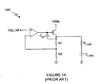
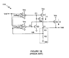
- An alternative approach as shown in a prior art voltage down converter FIGURE 1B is to add an additional transistor to the output of the voltage down converter in order to supply fluctuating current demands of the memory.
- this solution is not appropriate for embedded memories that have many diverse operations such as single read and write or read or write concurrent with a refresh operation, each type of operation sinking different amounts of current depending on the process, voltage, or temperature variations.
- the inherent delay of the comparators used in this approach is not sufficient to maintain a steady voltage level in the voltage down converter output. This is especially the situation in memories operating at high frequencies.
- a VDC may be used in various applications to supply large amount of "AC" type current (e.g., alternating or fluctuating current) while sustaining the necessary "DC” type current (e.g., a fixed current) and a steady DC voltage level.
- the conventional VDC design has some drawbacks when employed in modem applications, which often require large, fluctuating output currents.
- the VDC will typically require a relatively large source follower transistor.
- a corresponding comparator In order to drive such a large transistor, a corresponding comparator has to be relatively powerful. The relatively large transistor and comparator size results in substantial and undesirable current consumption for the VDC.
- the feedback or coupling capacitor must be relatively large in size to stabilize the VDC.
- the performance-to-power ratio of this type of conventional VDC diminishes with increasing current supply requirements.
- the conventional VDC eventually becomes sluggish to supply adequate AC current for digital circuits.
- the VDC cannot maintain the output voltage V pp at a steady level and voltage level dipping occurs.
- a large dip in voltage level can cause memory cells to fail. Accordingly, there is a need to keep V pp stable even while the memory device is operated at high frequencies for various operations each requiring high current demands.
- the VDC 110 in prior art FIGURE 1B includes comparators 170 and 171, a relatively large PMOS (positive channel metal oxide semiconductor) transistor 151 and a relatively small PMOS transistor 152, and a feedback compensation or coupling capacitor Pcc.
- Comparators 170 and 171 receive two inputs, a reference voltage (Vref) input and feedback loop input (Vfb). The output of the comparator 170 is coupled to the gate of transistor 151 while the output of the comparator 171 is coupled to the gate of transistor 171 and to the gate of transistor 153.
- Transistor 170 has a high gain but a low speed response to the signal that it receives in its gate, while transistor 171 has a low gain but a high frequency response.
- VDC 110 as shown in FIGURE 1B does not operate well for high frequency memories. This is due to the fact that the analog circuit shown by VDC 110 is inherently slow and cannot function well within ever increasing memory speeds where activity on the load is quickly changing. More specifically, the comparator requires a minimum difference between the reference voltage and the feedback voltage in order to change its output and to increase or decrease the current provided to the output node D1.
- the object of the invention is to remedy the drawbacks set out above by providing a voltage down converter that including an active driver having little driving capability with additional transistor pairs having separate digital control outputs and precisely controlling the down-voltage and stabilize the down voltage level without adding a huge reservoir capacitor.
- the present invention includes a voltage down converter for providing a supply voltage and current to a high-speed memory device as claimed in claim 1.
- the present invention includes a method of providing a supply voltage and current to a high-speed memory device using a voltage down converter as claimed in claim 10.
- VDC Voltage Down Converter
- the VDC of the invention is designed to generate a substantially constant high voltage VPP, that is greater than the logic "1" voltage level stored in a memory cell.
- the present VDC uses the external high voltage provided to an input pin of an integrated circuit that has a memory circuit, in order to generate the VPP voltage without the use of a charge pump.
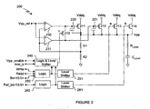
- the VDC includes a standby main driver 211 with high gain and low frequency response, an active driver 212 with low gain and high frequency response, and two additional transistors 213, 214, and the relevant circuitry such as a regulator 230, 231.
- the main driver 211 and the active driver 212 are implemented in a series pass configuration.
- the two additional transistors 213, 214 are in the form of PMOS drivers and receive in their gate a digital control signal.
- additional transistors 213, 214 will be hereinafter referenced as “active charge injector transistors.”
- active charge injector transistors While, it should be well understood that such nomenclature including the term “charge injector” should not be considered as limiting such elements to any previously understood or known definition of “charge injector transistor” or “active charge injector transistor.”
- the charge injector transistors 213, 214 are used to provide a pulsed increase in the current into the VPP voltage power supply node, to compensate for the load current increases occurring during read, write and/or refresh active operations.
- the charge injector transistor is implemented in a series pass configuration.
- the signal that controls the operation of the charge injector transistors 213, 214 is generated during the read, write and/or refresh operations or in anticipation of such operations.
- the dimensions of the charge injector transistors 213, 214 are designed to provide the necessary current that is sufficient to compensate for the increase in the load during an active cycle.
- the time that the control signal is applied to turn on the charge injector transistors is set so that the required amount of load-compensating current is supplied through these transistors 213, 214 to the VPP voltage output, so the VPP voltage level is maintained stable during the read, write and/or refresh operations.
- the time of the active pulse is programmed to compensate for temperature, voltage and process variations.
- FIGURE 2 includes a regulator that is shown as two comparators 230, 231 that include a PMOS current mirror load and two NMOS (negative channel metal oxide semiconductor) series-connected differential inputs and bias control NMOS connected to ground.
- Decoding logic is used to combine the read, write, and refresh operations with information of which single or double memory bank is accessed, to generate a control signal to enable one active charge injector transistor.
- Such decoding logic 240, 250, 260 and level shifter elements 251, 261 are embodied by appropriate circuitry (e.g., D-flip flops and logic gates) well known within the area of digital circuits and need not be further described herein. Numerous examples of level shifters exist throughout the prior art and may be used without straying from the intended scope of the present invention.
- the PMOS switch 210 shown in FIGURE 2 advantageously increases the stability of the negative feedback amplifier.
- This switch 210 is only selectively active. During the power-up stage and the recovery of Vpp level after re-enabling Vpp regulation by the Vpp-enable signal, the switch 210 is turned on and operated together with the standby main PMOS driver 211 to prevent the oscillation of Vpp from the active driver 212.
- a first active command such as read or write turns this switch 210 off so that the active driver 212 is independently operated.
- the Miller compensation capacitor 220 shown in FIGURE 2 prevents the Vpp oscillation caused by the small load capacitance C Load and high Vpp current.
- the steady driver can be operated with more stability by this Miller capacitor that, for example, may be in the range of 10pF.
- a second Miller compensation capacitor 221 is shown that has the same functionality as capacitor 220, though with a much reduced size, for example, in the range of 2pF. Reducing the size of this second capacitor 221 greatly facilitates application of the inventive VCD within smaller and smaller high-speed memory devices.
- elements 211 through 214 include four PMOS drivers including a steady driver 211, an active driver 212, an active charge injector transistor 213 for read/write, and an active charge injector transistor 214 for refresh. While only two active charge injector transistors 213, 214 are shown, it should be understood that more than two are possible if additional command functions beyond read, write, read and refresh, write and refresh and refresh operations are performed. Similarly, it should be readily apparent that only one active charge injector transistor is required to perform the function in accordance with the present invention if a refresh operation is not performed in parallel to the read or write operations. For illustration purposes though, two charge injector transistors 213, 214 are shown. Such additional active charge injector transistors should therefore be considered to be well within the intended scope of the present invention.
- the steady driver 211 takes control of Vpp.
- the active driver 212 has the same gate control level as the steady driver 211. However, after asserting a first command, the active driver 212 operates independently according to Vpp level in order to respond quickly.
- the active charge injector transistors 213, 214 each operate in relation to a corresponding command insertion - e.g., the active charge injector transistor 213 of read and write is activated upon a read command. In this way, two separate PMOS are able to easily react to the peak current of single word line access and double word lines. One PMOS charge injection current is trimmed as much as the requirement of a single command, that is, a single word line activation.
- the steady driver 211 will have a large transistor width relative to the active driver 212.
- each active charge injector transistor 213, 214 will have even smaller transistor widths than the active driver 212.
- the active charge injector transistors 213, 214 may have a small W/2 transistor width, but may be 1 ⁇ 4 width or less depending upon the given architecture and related load on the given array. Such modifications are possible so long as the size of the transistors is enough to compensate for current load of performing an active cycle in the memory.
- the active driver 212 moves down faster than the steady driver 211 because of the small Miller compensation capacitor 220 and small driver size.
- drastic voltage drop is avoided by the active charge injector transistor operation such that the active charge injector transistors 213, 214 preserve the Vpp level without using complicated control logic decoding.
- the charge injector transistor logic is implemented using delays and D-flip flops where the additional logic is negligible relative to known manner of providing a huge reservoir capacitor to be able to keep Vpp at a desired level.
- the fast response of the active charge injector transistor elements 213, 214 does not require any feedback loop to ensure the quick recovery of Vpp level.
- PVT variation of the Vpp level and current consumption can be tuned by pulse width control for process variation. Voltage and temperature variation are basically resolved with PMOS driver temperature and voltage variation of turn-on current without trimming.
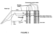
- the three relevant states of operation in regard to the VCD of the present invention include power-up, standby mode, and consecutive active mode.
- Vpp and control signals seek the corresponding levels to follow the intermittent Vpp reference level until a source voltage of Vpp ( Vddq in this example) boosts up to the determined level. In this way, large current is not issued because of a long power-up time.
- Vddq source voltage of Vpp
- standby mode static DC current by transistor leakage is invoked where no significant transient from the Vpp load capacitor C Load occurs and the steady and active drivers are tied together through the PMOS switch 210.
- the regulator 230, 231 finds the final optimized Vpp level according to the Vpp reference voltage level. Any steady voltage drop of Vpp is compensated from the steady 211 and active 212 drivers.
- the word line activation and relevant circuitry such as the level shifter 251 or 261 into a word line control block.
- the Vpp level drops abruptly.
- the active charge injector transistors are enabled depending on the command types such as single bank access (e.g., single read or write or refresh) and double bank access (e.g., read or write with concurrent refresh).
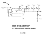
- FIGURE 4 is a simplified version of FIGURE 2 that illustrates operation of the VCD circuit in power-up and standby modes
- FIGURE 4 shows that the steady 211 and active 212 drivers are driven by the two regulators 230, 231 so as to determine the Vpp level for power-up and standby mode.
- the regulator 230, 231 takes a control of the Vpp level with Vpp_ref that is set by the reference generator.
- power-up and standby mode i.e., steady state
- only the steady 211 and active 212 drivers are activated and electrically tied together through PMOS switch 210.
- all drivers 211 through 214 including the active charge injector transistors 213, 214 are activated to quickly restore the Vpp level without any significant drop of Vpp level. Further, the pulse width of the control signal provided to the gates of the charge injector transistors 213, 214 is trimmable so that the VCD 200 b can supply as much as whatever Vpp current is sunk by the active operations of the memory.
- FIGURE 6 is a graphical illustration that shows a simplified version of Vpp with an addition of an active charge injector transistor in accordance with the present invention and Vpp without an active charge injector transistor.
- the top graph in FIGURE 6 shows a load current with two peaks in the load that indicate an active cycle in the memory array in which an operation occurs such as read, write, or refresh.
- the impact on Vpp without the benefit of an active charge injector transistor is shown at the bottom graph where Vpp initially drops upon increase in load current, fails to fully recover, drops again upon a second increase in load current, and subsequently slowly recovers to full value.
- Vpp with charge injector transistor shows the impact of the present invention on Vpp whereby Vpp suffers from only minor fluctuations and regains full value quickly after each increase in load current.
- the graph labelled "charge injector transistor control signal” is provided to indicate activation of the active charge injector transistor. Though over-simplified for purposes of illustration, it should be noted that a slight delay of course occurs from the time activity in the array begins until the time that a pulse is provided to the active charge injector transistor.
- the activation of the charge injector transistor can be set to start at the time that the word line drivers are activated, so the current load is quickly compensated.
- the activation of the charge injector transistor can be set to be earlier than the activation of the word line drivers so a drop on the Vpp voltage level is avoided completely. It would be obvious to someone skilled in the art that trimming can be used to set the best results and achieve the best stability of the Vpp voltage or to better accommodate the particular needs of their memories.
- the present invention is useful in any small sized memory with high-speed operation including, but not limited to, embedded DRAM. It is especially useful where developers are unable to acquire enough space on-chip to place a huge reservoir capacitor, especially within devices having an operating frequency over 700MHz.
- the present invention may be provided in a multi-bank version such that several separate banks of memory on a single chip may be served by multiple VCDs in accordance with the present invention. For instance, four memory blocks may be made independent such that access can differ where perhaps a first memory block may be read while a second memory block may be written. In such instance, the present invention may be provided in a multiple format to serve each block independently.
- the present invention also reduces the need for embedded memory to have an independent external power supply to resolve large drops within any internal power source.
- the present invention further presents a VCD with fast operation of over 1 GHz with a large Vpp current and a very small physical size requirement that are all important features of embedded memory products.
Landscapes
- Engineering & Computer Science (AREA)
- Power Engineering (AREA)
- Microelectronics & Electronic Packaging (AREA)
- Computer Hardware Design (AREA)
- Dram (AREA)
- Static Random-Access Memory (AREA)
- Continuous-Control Power Sources That Use Transistors (AREA)
- Read Only Memory (AREA)
Claims (10)
- Spannungsabwärtswandler (200), um eine Versorgungsspannung (Vpp) bzw. Versorgungsstrom zu einer Hochgeschwindigkeitsspeichervorrichtung zu liefern, wobei der Wandler gekennzeichnet ist durch:eine erste Treiberschaltung, die einen ersten Komparator (230) und einen stabilen Treibertransistor (211) mit einer großen Transistorbreite beinhaltet, und eine zweite Treiberschaltung, die einen zweiten Komparator (231) und einen aktiven Treibertransistor (212) mit einer kleinen Transistorbreite relativ zu dem stabilen Treiber beinhaltet, wobei die erste und die zweite Treiberschaltung einen wesentlichen Teil der Versorgungsspannung bzw. Versorgungsstrom zu der Hochgeschwindigkeitsspeichervorrichtung liefern;eine erste Logikschaltung (240), um die erste Treiberschaltung und die zweite Treiberschaltung schaltbar zu verbinden, um die Versorgungsspannung zu stabilisieren;eine zweite Logikschaltung (250, 251), um einen aktiven Befehl zu liefern, der das Vorhandensein einer Aktivität angibt; undmindestens einen zusätzlichen Transistor (213), um einen zusätzlichen Versorgungsstrom zu dem wesentlichen Teil zu liefern, und zwar in Reaktion auf den aktiven Befehl.
- Wandler nach Anspruch 1, bei dem die erste Logikschaltung die erste Treiberschaltung und die zweite Treiberschaltung über einen Transistorschalter (210) verbindet.
- Wandler nach Anspruch 2, bei dem der Transistorschalter, in Reaktion auf ein Ausgangssignal der ersten Logikschaltung, während des Einschaltens der Hochgeschwindigkeitsspeichervorrichtung eine Basis des stabilen Treibertransistors mit einer Basis des aktiven Treibertransistors verbindet.
- Wandler nach Anspruch 2, bei dem der Transistorschalter, in Reaktion auf ein Ausgangssignal der ersten Logikschaltung, während des Einschaltens der Hochgeschwindigkeitsspeichervorrichtung einen Ausgang des ersten Komparators zusammen mit einem Ausgang des zweiten Komparators auf die Basen von sowohl dem stabilen Treibertransistor als auch dem aktiven Treibertransistor zieht.
- Wandler nach Anspruch 2, bei dem die zweite Logikschaltung eine Kombinationslogikschaltung (250) und eine Pegelverschiebeschaltung (251) aufweist, die den aktiven Befehl liefert, der ein Impulssignal bildet, um den mindestens einen zusätzlichen Transistor zu aktivieren, um die zusätzliche Versorgungsspannung bzw. Versorgungsstrom so zu steuern, dass der wesentliche Teil der Versorgungsspannung bzw. Versorgungsstrom, kombiniert mit der zusätzlichen Versorgungsspannung bzw. Versorgungsstrom, während des Vorhandenseins der Aktivität Betriebslastverluste kompensiert.
- Wandler nach Anspruch 5, bei dem die Aktivität aus der Gruppe ausgewählt ist, die das Lesen aus einem Speicher, das Schreiben in einen Speicher und das Auffrischen eines Speichers beinhaltet.
- Wandler nach Anspruch 5, außerdem mit
einem zweiten zusätzlichen Transistor (214) und
einer dritten Logikschaltung, die eine weitere Kombinationslogikschaltung (260) und eine zugehörige Pegelverschiebeschaltung (261) beinhaltet, die einen zweiten aktiven Befehl liefert, der das Vorhandensein einer zusätzlichen Aktivität angibt, wobei der zweite aktive Befehl ein zweites Impulssignal bildet, um den zweiten zusätzlichen Transistor zu aktivieren, um eine weitere zusätzliche Versorgungsspannung bzw. Versorgungsstrom so zu steuern, dass der wesentliche Teil der Versorgungsspannung bzw. Versorgungsstrom, kombiniert mit sowohl der zusätzlichen Versorgungsspannung bzw. Versorgungsstrom als auch mit der weiteren zusätzlichen Versorgungsspannung bzw. Versorgungsstrom, während des Auftretens der Aktivität und der zusätzlichen Aktivität Betriebslastverluste kompensiert. - Wandler nach Anspruch 7, bei dem die Aktivität aus der Gruppe ausgewählt ist, die das Lesen aus einem Speicher und das Schreiben in einen Speicher beinhaltet.
- Wandler nach Anspruch 8, bei dem die zusätzliche Aktivität das Auffrischen eines Speichers ist.
- Verfahren, um eine Versorgungsspannung bzw. Versorgungsstroms zu einer Hochgeschwindigkeitsspeichervorrichtung zu liefern, und zwar unter Verwendung des Spannungsabwärtswandlers nach einem der Ansprüche 1-9, wobei das Verfahren umfasst:Liefern des wesentlichen Teils der Versorgungsspannung bzw. Versorgungsstrom, indem ein stabiler Strom mittels der ersten Treiberschaltung zu der Speichervorrichtung geliefert wird und indem eine schwankender Strom mittels der zweiten Treiberschaltung zu der Speichervorrichtung geliefert wird; undLiefern eines zusätzlichen Stroms zu dem wesentlichen Teil mittels des mindestens einen zusätzlichen Transistors in Reaktion auf den aktiven Befehl, der das Vorhandensein einer Aktivität angibt.
Applications Claiming Priority (2)
| Application Number | Priority Date | Filing Date | Title |
|---|---|---|---|
| US11/195,641 US7248531B2 (en) | 2005-08-03 | 2005-08-03 | Voltage down converter for high speed memory |
| PCT/CA2006/001252 WO2007014461A1 (en) | 2005-08-03 | 2006-07-31 | Voltage down converter for high speed memory |
Publications (3)
| Publication Number | Publication Date |
|---|---|
| EP1913596A1 EP1913596A1 (de) | 2008-04-23 |
| EP1913596A4 EP1913596A4 (de) | 2009-03-25 |
| EP1913596B1 true EP1913596B1 (de) | 2010-10-06 |
Family
ID=37708517
Family Applications (1)
| Application Number | Title | Priority Date | Filing Date |
|---|---|---|---|
| EP06761198A Active EP1913596B1 (de) | 2005-08-03 | 2006-07-31 | Spannungs-abwärtswandler für schnellen speicher |
Country Status (8)
| Country | Link |
|---|---|
| US (5) | US7248531B2 (de) |
| EP (1) | EP1913596B1 (de) |
| JP (1) | JP4901867B2 (de) |
| KR (2) | KR101324859B1 (de) |
| AT (1) | ATE484057T1 (de) |
| DE (1) | DE602006017382D1 (de) |
| TW (3) | TW201346925A (de) |
| WO (1) | WO2007014461A1 (de) |
Cited By (1)
| Publication number | Priority date | Publication date | Assignee | Title |
|---|---|---|---|---|
| DE102020105749A1 (de) | 2020-02-11 | 2021-08-12 | Taiwan Semiconductor Manufacturing Co., Ltd. | Neuartiges on-chip-stromversorgungsregelungssystem fürmram-operationen |
Families Citing this family (35)
| Publication number | Priority date | Publication date | Assignee | Title |
|---|---|---|---|---|
| US7518434B1 (en) * | 2005-09-16 | 2009-04-14 | Cypress Semiconductor Corporation | Reference voltage circuit |
| US20070126494A1 (en) * | 2005-12-06 | 2007-06-07 | Sandisk Corporation | Charge pump having shunt diode for improved operating efficiency |
| US20070139099A1 (en) * | 2005-12-16 | 2007-06-21 | Sandisk Corporation | Charge pump regulation control for improved power efficiency |
| US7372320B2 (en) * | 2005-12-16 | 2008-05-13 | Sandisk Corporation | Voltage regulation with active supplemental current for output stabilization |
| US20070229149A1 (en) * | 2006-03-30 | 2007-10-04 | Sandisk Corporation | Voltage regulator having high voltage protection |
| US7554311B2 (en) * | 2006-07-31 | 2009-06-30 | Sandisk Corporation | Hybrid charge pump regulation |
| DE102006036349B4 (de) * | 2006-08-03 | 2015-04-02 | Infineon Technologies Ag | Schaltungsvorrichtung und Verfahren zum Erkennen eines Betriebszustandes |
| KR100846392B1 (ko) * | 2006-08-31 | 2008-07-15 | 주식회사 하이닉스반도체 | 반도체 메모리 장치 |
| US7368979B2 (en) | 2006-09-19 | 2008-05-06 | Sandisk Corporation | Implementation of output floating scheme for hv charge pumps |
| JP5130792B2 (ja) | 2007-06-08 | 2013-01-30 | 富士通セミコンダクター株式会社 | 半導体集積回路およびシステム |
| KR100937939B1 (ko) * | 2008-04-24 | 2010-01-21 | 주식회사 하이닉스반도체 | 반도체 소자의 내부전압 생성회로 |
| JP5160317B2 (ja) * | 2008-06-09 | 2013-03-13 | セイコーインスツル株式会社 | ボルテージレギュレータ |
| JP5308943B2 (ja) * | 2009-07-16 | 2013-10-09 | ルネサスエレクトロニクス株式会社 | 電源回路 |
| JP5361614B2 (ja) * | 2009-08-28 | 2013-12-04 | ルネサスエレクトロニクス株式会社 | 降圧回路 |
| RU2592719C2 (ru) * | 2012-03-16 | 2016-07-27 | Интел Корпорейшн | Генератор опорного напряжения с низким импедансом |
| CN103366804B (zh) * | 2012-03-30 | 2017-10-13 | 硅存储技术公司 | 具有电流注入读出放大器的非易失性存储装置 |
| US9213382B2 (en) * | 2012-09-12 | 2015-12-15 | Intel Corporation | Linear voltage regulator based on-die grid |
| US9201435B2 (en) * | 2013-03-05 | 2015-12-01 | Infineon Technologies Ag | System and method for a power supply |
| US20140266103A1 (en) * | 2013-03-15 | 2014-09-18 | Qualcomm Incorporated | Digitally assisted regulation for an integrated capless low-dropout (ldo) voltage regulator |
| KR102161826B1 (ko) * | 2013-11-13 | 2020-10-06 | 삼성전자주식회사 | 전압 컨버터, 이를 포함하는 무선 전력 수신 장치 및 무선 전력 전송 시스템 |
| KR101601432B1 (ko) * | 2014-06-17 | 2016-03-10 | 현대자동차주식회사 | 인젝터 구동 제어 장치 |
| JP5976077B2 (ja) * | 2014-11-14 | 2016-08-23 | 力晶科技股▲ふん▼有限公司 | 内部電源電圧発生回路、半導体記憶装置及び半導体装置 |
| JP6060239B1 (ja) * | 2015-10-21 | 2017-01-11 | トレックス・セミコンダクター株式会社 | 基準電圧発生回路 |
| US10250139B2 (en) * | 2016-03-31 | 2019-04-02 | Micron Technology, Inc. | Apparatuses and methods for a load current control circuit for a source follower voltage regulator |
| CN106708153B (zh) | 2017-03-08 | 2019-03-12 | 长江存储科技有限责任公司 | 一种高带宽低压差线性稳压器 |
| US10474174B2 (en) * | 2017-04-04 | 2019-11-12 | Intel Corporation | Programmable supply generator |
| US10505534B2 (en) * | 2017-04-06 | 2019-12-10 | Texas Instruments Incorporated | High voltage low current enable pin startup circuit |
| US10885967B2 (en) * | 2019-01-14 | 2021-01-05 | Micron Technology, Inc. | Systems and methods for improving power efficiency in refreshing memory banks |
| JP7001636B2 (ja) | 2019-06-05 | 2022-01-19 | ウィンボンド エレクトロニクス コーポレーション | 電圧生成回路 |
| TWI773018B (zh) * | 2019-09-06 | 2022-08-01 | 新唐科技股份有限公司 | 恢復升壓電路、用於電壓調節之電子電路及其方法 |
| CN113496720B (zh) * | 2020-04-03 | 2024-01-05 | 铁电存储器股份有限公司 | 电压供应电路、存储器单元装置、晶体管装置及其方法 |
| US11791725B2 (en) | 2020-08-06 | 2023-10-17 | Mediatek Inc. | Voltage regulator with hybrid control for fast transient response |
| US11942860B2 (en) | 2021-05-26 | 2024-03-26 | Murata Manufacturing Co., Ltd. | Dynamic division ratio charge pump switching |
| US11936371B1 (en) | 2022-10-04 | 2024-03-19 | Psemi Corporation | Accurate reduced gate-drive current limiter |
| US12184174B2 (en) * | 2022-10-05 | 2024-12-31 | Murata Manufacturing Co., Ltd. | Reduced gate drive for power converter with dynamically switching ratio |
Family Cites Families (27)
| Publication number | Priority date | Publication date | Assignee | Title |
|---|---|---|---|---|
| US4254372A (en) * | 1979-02-21 | 1981-03-03 | General Motors Corporation | Series pass voltage regulator with overcurrent protection |
| US4395675A (en) * | 1981-10-22 | 1983-07-26 | Bell Telephone Laboratories, Incorporated | Transformerless noninverting buck boost switching regulator |
| US5184031A (en) * | 1990-02-08 | 1993-02-02 | Kabushiki Kaisha Toshiba | Semiconductor integrated circuit |
| JPH07122992B2 (ja) * | 1990-02-08 | 1995-12-25 | 株式会社東芝 | 半導体集積回路 |
| JPH07105682A (ja) * | 1993-10-06 | 1995-04-21 | Nec Corp | ダイナミックメモリ装置 |
| KR0131746B1 (ko) * | 1993-12-01 | 1998-04-14 | 김주용 | 내부 강압전원 회로 |
| US5563500A (en) * | 1994-05-16 | 1996-10-08 | Thomson Consumer Electronics, Inc. | Voltage regulator having complementary type transistor |
| JP3705842B2 (ja) * | 1994-08-04 | 2005-10-12 | 株式会社ルネサステクノロジ | 半導体装置 |
| US5806692A (en) * | 1995-11-22 | 1998-09-15 | The Taper Corporation | Apparatus for storage and display of personal communication devices |
| JP4074697B2 (ja) * | 1997-11-28 | 2008-04-09 | 株式会社ルネサステクノロジ | 半導体装置 |
| JP4424770B2 (ja) * | 1998-12-25 | 2010-03-03 | 株式会社ルネサステクノロジ | 半導体記憶装置 |
| KR100319606B1 (ko) * | 1999-02-12 | 2002-01-05 | 김영환 | 전압 강압 회로 |
| US6140805A (en) * | 1999-05-18 | 2000-10-31 | Kabushiki Kaisha Toshiba | Source follower NMOS voltage regulator with PMOS switching element |
| JP4822572B2 (ja) * | 1999-09-02 | 2011-11-24 | ルネサスエレクトロニクス株式会社 | 半導体記憶装置 |
| JP4271812B2 (ja) * | 2000-01-31 | 2009-06-03 | 富士通マイクロエレクトロニクス株式会社 | 半導体装置の内部電源電圧生成回路の制御方法、半導体記憶装置の内部電源電圧生成回路の制御方法及び半導体記憶装置の内部電源電圧生成回路 |
| JP2002008374A (ja) * | 2000-06-22 | 2002-01-11 | Mitsubishi Electric Corp | 電圧降圧回路 |
| JP2002042467A (ja) * | 2000-07-21 | 2002-02-08 | Mitsubishi Electric Corp | 電圧降圧回路およびそれを備える半導体集積回路装置 |
| KR100518399B1 (ko) * | 2000-07-25 | 2005-09-29 | 엔이씨 일렉트로닉스 가부시키가이샤 | 내부 전압 레벨 제어 회로 및 반도체 기억 장치 및 그들의제어 방법 |
| JP2002074956A (ja) * | 2000-09-04 | 2002-03-15 | Mitsubishi Electric Corp | 半導体装置 |
| JP2003015751A (ja) * | 2001-07-03 | 2003-01-17 | Matsushita Electric Ind Co Ltd | 高電圧発生回路 |
| JP2003022697A (ja) * | 2001-07-06 | 2003-01-24 | Mitsubishi Electric Corp | 半導体集積回路装置 |
| JP3983612B2 (ja) * | 2002-07-08 | 2007-09-26 | ローム株式会社 | 電流制限機能付き安定化電源装置 |
| US6806692B2 (en) * | 2002-11-22 | 2004-10-19 | Giga Semiconductor, Inc. | Voltage down converter |
| KR100543659B1 (ko) * | 2003-06-20 | 2006-01-20 | 주식회사 하이닉스반도체 | 내부전압 생성용 액티브 드라이버 |
| JP2005117442A (ja) * | 2003-10-09 | 2005-04-28 | Renesas Technology Corp | 半導体集積回路 |
| EP1653315A1 (de) * | 2004-10-28 | 2006-05-03 | STMicroelectronics S.r.l. | Verbesserter Spannungsabwärtswandler |
| EP1667158B1 (de) * | 2004-10-28 | 2007-01-31 | STMicroelectronics S.r.l. | Spannungs-Abwärts-Wandler mit reduzierter Welligkeit |
-
2005
- 2005-08-03 US US11/195,641 patent/US7248531B2/en not_active Expired - Fee Related
-
2006
- 2006-07-31 KR KR1020087005295A patent/KR101324859B1/ko active Active
- 2006-07-31 AT AT06761198T patent/ATE484057T1/de not_active IP Right Cessation
- 2006-07-31 DE DE602006017382T patent/DE602006017382D1/de active Active
- 2006-07-31 WO PCT/CA2006/001252 patent/WO2007014461A1/en not_active Ceased
- 2006-07-31 KR KR1020137006196A patent/KR101434121B1/ko active Active
- 2006-07-31 EP EP06761198A patent/EP1913596B1/de active Active
- 2006-07-31 JP JP2008524330A patent/JP4901867B2/ja not_active Expired - Fee Related
- 2006-08-02 TW TW102128328A patent/TW201346925A/zh unknown
- 2006-08-02 TW TW095128339A patent/TWI430277B/zh active
- 2006-08-02 TW TW102128327A patent/TW201346924A/zh unknown
-
2007
- 2007-07-23 US US11/781,581 patent/US7593281B2/en not_active Expired - Lifetime
-
2009
- 2009-07-17 US US12/505,069 patent/US8164968B2/en not_active Expired - Lifetime
-
2012
- 2012-03-19 US US13/423,901 patent/US8611171B2/en not_active Expired - Lifetime
-
2013
- 2013-11-14 US US14/080,302 patent/US20140071781A1/en not_active Abandoned
Cited By (1)
| Publication number | Priority date | Publication date | Assignee | Title |
|---|---|---|---|---|
| DE102020105749A1 (de) | 2020-02-11 | 2021-08-12 | Taiwan Semiconductor Manufacturing Co., Ltd. | Neuartiges on-chip-stromversorgungsregelungssystem fürmram-operationen |
Also Published As
| Publication number | Publication date |
|---|---|
| US8611171B2 (en) | 2013-12-17 |
| US20120176118A1 (en) | 2012-07-12 |
| WO2007014461A1 (en) | 2007-02-08 |
| TWI430277B (zh) | 2014-03-11 |
| US20080186790A1 (en) | 2008-08-07 |
| US8164968B2 (en) | 2012-04-24 |
| KR20080039471A (ko) | 2008-05-07 |
| TW200713302A (en) | 2007-04-01 |
| JP2009503705A (ja) | 2009-01-29 |
| US20070030749A1 (en) | 2007-02-08 |
| DE602006017382D1 (de) | 2010-11-18 |
| US7593281B2 (en) | 2009-09-22 |
| ATE484057T1 (de) | 2010-10-15 |
| JP4901867B2 (ja) | 2012-03-21 |
| EP1913596A1 (de) | 2008-04-23 |
| TW201346925A (zh) | 2013-11-16 |
| KR20130042614A (ko) | 2013-04-26 |
| KR101324859B1 (ko) | 2013-11-01 |
| KR101434121B1 (ko) | 2014-08-26 |
| US20140071781A1 (en) | 2014-03-13 |
| EP1913596A4 (de) | 2009-03-25 |
| US20090279375A1 (en) | 2009-11-12 |
| US7248531B2 (en) | 2007-07-24 |
| TW201346924A (zh) | 2013-11-16 |
Similar Documents
| Publication | Publication Date | Title |
|---|---|---|
| EP1913596B1 (de) | Spannungs-abwärtswandler für schnellen speicher | |
| KR100518399B1 (ko) | 내부 전압 레벨 제어 회로 및 반도체 기억 장치 및 그들의제어 방법 | |
| KR100394757B1 (ko) | 반도체 장치 | |
| US8040177B2 (en) | Internal voltage generating circuit of semiconductor device | |
| US7576596B2 (en) | Internal voltage generator of semiconductor device | |
| US20040207458A1 (en) | Voltage booster power supply circuit | |
| KR20040014151A (ko) | 안정 동작이 가능한 반도체 기억 장치 | |
| KR100309602B1 (ko) | 전위검출회로에서의전력소비를감소시키는반도체장치 | |
| US20140307499A1 (en) | Booster circuit | |
| US20040075422A1 (en) | Voltage regulator with very quick response | |
| US5774405A (en) | Dynamic random access memory having an internal circuit using a boosted potential | |
| KR100252427B1 (ko) | 전압 발생 회로를 구비한 반도체 장치 | |
| JP3869690B2 (ja) | 内部電圧レベル制御回路および半導体記憶装置並びにそれらの制御方法 | |
| KR100977731B1 (ko) | 반도체 메모리 장치의 네거티브 워드라인 전압 발생기 | |
| JPH08339682A (ja) | 半導体記憶装置 | |
| US7298199B2 (en) | Substrate bias voltage generating circuit for use in a semiconductor memory device | |
| US12362001B2 (en) | Voltage generating circuit and memory | |
| JP2010136573A (ja) | 昇圧電圧発生回路、負電圧発生回路および降圧電圧発生回路 |
Legal Events
| Date | Code | Title | Description |
|---|---|---|---|
| PUAI | Public reference made under article 153(3) epc to a published international application that has entered the european phase |
Free format text: ORIGINAL CODE: 0009012 |
|
| 17P | Request for examination filed |
Effective date: 20080129 |
|
| AK | Designated contracting states |
Kind code of ref document: A1 Designated state(s): AT BE BG CH CY CZ DE DK EE ES FI FR GB GR HU IE IS IT LI LT LU LV MC NL PL PT RO SE SI SK TR |
|
| A4 | Supplementary search report drawn up and despatched |
Effective date: 20090225 |
|
| 17Q | First examination report despatched |
Effective date: 20090618 |
|
| GRAP | Despatch of communication of intention to grant a patent |
Free format text: ORIGINAL CODE: EPIDOSNIGR1 |
|
| DAX | Request for extension of the european patent (deleted) | ||
| GRAS | Grant fee paid |
Free format text: ORIGINAL CODE: EPIDOSNIGR3 |
|
| GRAA | (expected) grant |
Free format text: ORIGINAL CODE: 0009210 |
|
| RAP1 | Party data changed (applicant data changed or rights of an application transferred) |
Owner name: MOSAID TECHNOLOGIES INCORPORATED |
|
| AK | Designated contracting states |
Kind code of ref document: B1 Designated state(s): AT BE BG CH CY CZ DE DK EE ES FI FR GB GR HU IE IS IT LI LT LU LV MC NL PL PT RO SE SI SK TR |
|
| REG | Reference to a national code |
Ref country code: GB Ref legal event code: FG4D |
|
| REG | Reference to a national code |
Ref country code: CH Ref legal event code: EP |
|
| REG | Reference to a national code |
Ref country code: IE Ref legal event code: FG4D |
|
| REF | Corresponds to: |
Ref document number: 602006017382 Country of ref document: DE Date of ref document: 20101118 Kind code of ref document: P |
|
| REG | Reference to a national code |
Ref country code: NL Ref legal event code: VDEP Effective date: 20101006 |
|
| PG25 | Lapsed in a contracting state [announced via postgrant information from national office to epo] |
Ref country code: SI Free format text: LAPSE BECAUSE OF FAILURE TO SUBMIT A TRANSLATION OF THE DESCRIPTION OR TO PAY THE FEE WITHIN THE PRESCRIBED TIME-LIMIT Effective date: 20101006 |
|
| LTIE | Lt: invalidation of european patent or patent extension |
Effective date: 20101006 |
|
| PG25 | Lapsed in a contracting state [announced via postgrant information from national office to epo] |
Ref country code: LT Free format text: LAPSE BECAUSE OF FAILURE TO SUBMIT A TRANSLATION OF THE DESCRIPTION OR TO PAY THE FEE WITHIN THE PRESCRIBED TIME-LIMIT Effective date: 20101006 |
|
| PG25 | Lapsed in a contracting state [announced via postgrant information from national office to epo] |
Ref country code: PT Free format text: LAPSE BECAUSE OF FAILURE TO SUBMIT A TRANSLATION OF THE DESCRIPTION OR TO PAY THE FEE WITHIN THE PRESCRIBED TIME-LIMIT Effective date: 20110207 Ref country code: FI Free format text: LAPSE BECAUSE OF FAILURE TO SUBMIT A TRANSLATION OF THE DESCRIPTION OR TO PAY THE FEE WITHIN THE PRESCRIBED TIME-LIMIT Effective date: 20101006 Ref country code: NL Free format text: LAPSE BECAUSE OF FAILURE TO SUBMIT A TRANSLATION OF THE DESCRIPTION OR TO PAY THE FEE WITHIN THE PRESCRIBED TIME-LIMIT Effective date: 20101006 Ref country code: BG Free format text: LAPSE BECAUSE OF FAILURE TO SUBMIT A TRANSLATION OF THE DESCRIPTION OR TO PAY THE FEE WITHIN THE PRESCRIBED TIME-LIMIT Effective date: 20110106 Ref country code: IS Free format text: LAPSE BECAUSE OF FAILURE TO SUBMIT A TRANSLATION OF THE DESCRIPTION OR TO PAY THE FEE WITHIN THE PRESCRIBED TIME-LIMIT Effective date: 20110206 Ref country code: LV Free format text: LAPSE BECAUSE OF FAILURE TO SUBMIT A TRANSLATION OF THE DESCRIPTION OR TO PAY THE FEE WITHIN THE PRESCRIBED TIME-LIMIT Effective date: 20101006 Ref country code: AT Free format text: LAPSE BECAUSE OF FAILURE TO SUBMIT A TRANSLATION OF THE DESCRIPTION OR TO PAY THE FEE WITHIN THE PRESCRIBED TIME-LIMIT Effective date: 20101006 Ref country code: SE Free format text: LAPSE BECAUSE OF FAILURE TO SUBMIT A TRANSLATION OF THE DESCRIPTION OR TO PAY THE FEE WITHIN THE PRESCRIBED TIME-LIMIT Effective date: 20101006 |
|
| PG25 | Lapsed in a contracting state [announced via postgrant information from national office to epo] |
Ref country code: GR Free format text: LAPSE BECAUSE OF FAILURE TO SUBMIT A TRANSLATION OF THE DESCRIPTION OR TO PAY THE FEE WITHIN THE PRESCRIBED TIME-LIMIT Effective date: 20110107 Ref country code: BE Free format text: LAPSE BECAUSE OF FAILURE TO SUBMIT A TRANSLATION OF THE DESCRIPTION OR TO PAY THE FEE WITHIN THE PRESCRIBED TIME-LIMIT Effective date: 20101006 |
|
| PG25 | Lapsed in a contracting state [announced via postgrant information from national office to epo] |
Ref country code: ES Free format text: LAPSE BECAUSE OF FAILURE TO SUBMIT A TRANSLATION OF THE DESCRIPTION OR TO PAY THE FEE WITHIN THE PRESCRIBED TIME-LIMIT Effective date: 20110117 Ref country code: CZ Free format text: LAPSE BECAUSE OF FAILURE TO SUBMIT A TRANSLATION OF THE DESCRIPTION OR TO PAY THE FEE WITHIN THE PRESCRIBED TIME-LIMIT Effective date: 20101006 Ref country code: EE Free format text: LAPSE BECAUSE OF FAILURE TO SUBMIT A TRANSLATION OF THE DESCRIPTION OR TO PAY THE FEE WITHIN THE PRESCRIBED TIME-LIMIT Effective date: 20101006 |
|
| PLBE | No opposition filed within time limit |
Free format text: ORIGINAL CODE: 0009261 |
|
| STAA | Information on the status of an ep patent application or granted ep patent |
Free format text: STATUS: NO OPPOSITION FILED WITHIN TIME LIMIT |
|
| PG25 | Lapsed in a contracting state [announced via postgrant information from national office to epo] |
Ref country code: RO Free format text: LAPSE BECAUSE OF FAILURE TO SUBMIT A TRANSLATION OF THE DESCRIPTION OR TO PAY THE FEE WITHIN THE PRESCRIBED TIME-LIMIT Effective date: 20101006 Ref country code: PL Free format text: LAPSE BECAUSE OF FAILURE TO SUBMIT A TRANSLATION OF THE DESCRIPTION OR TO PAY THE FEE WITHIN THE PRESCRIBED TIME-LIMIT Effective date: 20101006 Ref country code: SK Free format text: LAPSE BECAUSE OF FAILURE TO SUBMIT A TRANSLATION OF THE DESCRIPTION OR TO PAY THE FEE WITHIN THE PRESCRIBED TIME-LIMIT Effective date: 20101006 Ref country code: DK Free format text: LAPSE BECAUSE OF FAILURE TO SUBMIT A TRANSLATION OF THE DESCRIPTION OR TO PAY THE FEE WITHIN THE PRESCRIBED TIME-LIMIT Effective date: 20101006 |
|
| 26N | No opposition filed |
Effective date: 20110707 |
|
| REG | Reference to a national code |
Ref country code: DE Ref legal event code: R097 Ref document number: 602006017382 Country of ref document: DE Effective date: 20110707 |
|
| PG25 | Lapsed in a contracting state [announced via postgrant information from national office to epo] |
Ref country code: MC Free format text: LAPSE BECAUSE OF NON-PAYMENT OF DUE FEES Effective date: 20110731 |
|
| REG | Reference to a national code |
Ref country code: CH Ref legal event code: PL |
|
| REG | Reference to a national code |
Ref country code: IE Ref legal event code: MM4A |
|
| PG25 | Lapsed in a contracting state [announced via postgrant information from national office to epo] |
Ref country code: LI Free format text: LAPSE BECAUSE OF NON-PAYMENT OF DUE FEES Effective date: 20110731 Ref country code: CH Free format text: LAPSE BECAUSE OF NON-PAYMENT OF DUE FEES Effective date: 20110731 |
|
| PG25 | Lapsed in a contracting state [announced via postgrant information from national office to epo] |
Ref country code: IE Free format text: LAPSE BECAUSE OF NON-PAYMENT OF DUE FEES Effective date: 20110731 |
|
| PG25 | Lapsed in a contracting state [announced via postgrant information from national office to epo] |
Ref country code: CY Free format text: LAPSE BECAUSE OF EXPIRATION OF PROTECTION Effective date: 20101006 Ref country code: LU Free format text: LAPSE BECAUSE OF NON-PAYMENT OF DUE FEES Effective date: 20110731 |
|
| PG25 | Lapsed in a contracting state [announced via postgrant information from national office to epo] |
Ref country code: TR Free format text: LAPSE BECAUSE OF FAILURE TO SUBMIT A TRANSLATION OF THE DESCRIPTION OR TO PAY THE FEE WITHIN THE PRESCRIBED TIME-LIMIT Effective date: 20101006 |
|
| PG25 | Lapsed in a contracting state [announced via postgrant information from national office to epo] |
Ref country code: HU Free format text: LAPSE BECAUSE OF FAILURE TO SUBMIT A TRANSLATION OF THE DESCRIPTION OR TO PAY THE FEE WITHIN THE PRESCRIBED TIME-LIMIT Effective date: 20101006 |
|
| REG | Reference to a national code |
Ref country code: DE Ref legal event code: R082 Ref document number: 602006017382 Country of ref document: DE Representative=s name: UEXKUELL & STOLBERG, DE |
|
| REG | Reference to a national code |
Ref country code: FR Ref legal event code: CD Owner name: CONVERSANT INTELLECTUAL PROPERTY MANAGEMENT IN, CA Effective date: 20141021 Ref country code: FR Ref legal event code: CA Effective date: 20141021 |
|
| PGFP | Annual fee paid to national office [announced via postgrant information from national office to epo] |
Ref country code: FR Payment date: 20140708 Year of fee payment: 9 Ref country code: GB Payment date: 20140730 Year of fee payment: 9 |
|
| PGFP | Annual fee paid to national office [announced via postgrant information from national office to epo] |
Ref country code: IT Payment date: 20140714 Year of fee payment: 9 |
|
| REG | Reference to a national code |
Ref country code: DE Ref legal event code: R081 Ref document number: 602006017382 Country of ref document: DE Owner name: CONVERSANT INTELLECTUAL PROPERTY MANAGEMENT IN, CA Free format text: FORMER OWNER: MOSAID TECHNOLOGIES INC., OTTAWA, ONTARIO, CA Effective date: 20141120 Ref country code: DE Ref legal event code: R082 Ref document number: 602006017382 Country of ref document: DE Representative=s name: UEXKUELL & STOLBERG, DE Effective date: 20141120 Ref country code: DE Ref legal event code: R082 Ref document number: 602006017382 Country of ref document: DE Representative=s name: UEXKUELL & STOLBERG PARTNERSCHAFT VON PATENT- , DE Effective date: 20141120 |
|
| GBPC | Gb: european patent ceased through non-payment of renewal fee |
Effective date: 20150731 |
|
| PG25 | Lapsed in a contracting state [announced via postgrant information from national office to epo] |
Ref country code: IT Free format text: LAPSE BECAUSE OF NON-PAYMENT OF DUE FEES Effective date: 20150731 Ref country code: GB Free format text: LAPSE BECAUSE OF NON-PAYMENT OF DUE FEES Effective date: 20150731 |
|
| REG | Reference to a national code |
Ref country code: FR Ref legal event code: ST Effective date: 20160331 |
|
| PG25 | Lapsed in a contracting state [announced via postgrant information from national office to epo] |
Ref country code: FR Free format text: LAPSE BECAUSE OF NON-PAYMENT OF DUE FEES Effective date: 20150731 |
|
| PGFP | Annual fee paid to national office [announced via postgrant information from national office to epo] |
Ref country code: DE Payment date: 20250604 Year of fee payment: 20 |