EP1887633B2 - Solar cell and solar cell manufacturing method - Google Patents
Solar cell and solar cell manufacturing method Download PDFInfo
- Publication number
- EP1887633B2 EP1887633B2 EP06745924.8A EP06745924A EP1887633B2 EP 1887633 B2 EP1887633 B2 EP 1887633B2 EP 06745924 A EP06745924 A EP 06745924A EP 1887633 B2 EP1887633 B2 EP 1887633B2
- Authority
- EP
- European Patent Office
- Prior art keywords
- bus bar
- bar electrode
- shape
- electrode
- solar cell
- Prior art date
- Legal status (The legal status is an assumption and is not a legal conclusion. Google has not performed a legal analysis and makes no representation as to the accuracy of the status listed.)
- Active
Links
- 238000004519 manufacturing process Methods 0.000 title claims description 6
- 239000000758 substrate Substances 0.000 claims description 33
- 239000004065 semiconductor Substances 0.000 claims description 24
- 238000010304 firing Methods 0.000 claims description 12
- 238000007639 printing Methods 0.000 claims description 12
- GYHNNYVSQQEPJS-UHFFFAOYSA-N Gallium Chemical compound [Ga] GYHNNYVSQQEPJS-UHFFFAOYSA-N 0.000 claims description 5
- 229910052733 gallium Inorganic materials 0.000 claims description 5
- 229910021421 monocrystalline silicon Inorganic materials 0.000 claims description 4
- 229910000679 solder Inorganic materials 0.000 description 14
- 239000000853 adhesive Substances 0.000 description 7
- 230000001070 adhesive effect Effects 0.000 description 7
- KWYUFKZDYYNOTN-UHFFFAOYSA-M Potassium hydroxide Chemical compound [OH-].[K+] KWYUFKZDYYNOTN-UHFFFAOYSA-M 0.000 description 6
- 239000007772 electrode material Substances 0.000 description 6
- 230000000052 comparative effect Effects 0.000 description 5
- 230000000694 effects Effects 0.000 description 5
- 238000000034 method Methods 0.000 description 5
- 238000007650 screen-printing Methods 0.000 description 4
- 230000015572 biosynthetic process Effects 0.000 description 3
- 238000006243 chemical reaction Methods 0.000 description 3
- 238000009792 diffusion process Methods 0.000 description 3
- 239000012535 impurity Substances 0.000 description 3
- OAICVXFJPJFONN-UHFFFAOYSA-N Phosphorus Chemical compound [P] OAICVXFJPJFONN-UHFFFAOYSA-N 0.000 description 2
- 239000007864 aqueous solution Substances 0.000 description 2
- 230000015556 catabolic process Effects 0.000 description 2
- 238000006731 degradation reaction Methods 0.000 description 2
- 150000004767 nitrides Chemical class 0.000 description 2
- 239000002245 particle Substances 0.000 description 2
- 239000011574 phosphorus Substances 0.000 description 2
- 229910052698 phosphorus Inorganic materials 0.000 description 2
- XHXFXVLFKHQFAL-UHFFFAOYSA-N phosphoryl trichloride Chemical compound ClP(Cl)(Cl)=O XHXFXVLFKHQFAL-UHFFFAOYSA-N 0.000 description 2
- 238000005268 plasma chemical vapour deposition Methods 0.000 description 2
- 235000011118 potassium hydroxide Nutrition 0.000 description 2
- 229910019213 POCl3 Inorganic materials 0.000 description 1
- XUIMIQQOPSSXEZ-UHFFFAOYSA-N Silicon Chemical compound [Si] XUIMIQQOPSSXEZ-UHFFFAOYSA-N 0.000 description 1
- BQCADISMDOOEFD-UHFFFAOYSA-N Silver Chemical compound [Ag] BQCADISMDOOEFD-UHFFFAOYSA-N 0.000 description 1
- 229910052782 aluminium Inorganic materials 0.000 description 1
- XAGFODPZIPBFFR-UHFFFAOYSA-N aluminium Chemical compound [Al] XAGFODPZIPBFFR-UHFFFAOYSA-N 0.000 description 1
- 239000011248 coating agent Substances 0.000 description 1
- 238000000576 coating method Methods 0.000 description 1
- 239000013078 crystal Substances 0.000 description 1
- 230000001419 dependent effect Effects 0.000 description 1
- 238000005530 etching Methods 0.000 description 1
- 229910021478 group 5 element Inorganic materials 0.000 description 1
- 238000005468 ion implantation Methods 0.000 description 1
- 239000007788 liquid Substances 0.000 description 1
- 238000005259 measurement Methods 0.000 description 1
- 238000005240 physical vapour deposition Methods 0.000 description 1
- 229910052710 silicon Inorganic materials 0.000 description 1
- 239000010703 silicon Substances 0.000 description 1
- 229910052709 silver Inorganic materials 0.000 description 1
- 239000004332 silver Substances 0.000 description 1
- 238000005476 soldering Methods 0.000 description 1
- 238000001228 spectrum Methods 0.000 description 1
- 238000001771 vacuum deposition Methods 0.000 description 1
Images

Classifications
-
- H—ELECTRICITY
- H01—ELECTRIC ELEMENTS
- H01L—SEMICONDUCTOR DEVICES NOT COVERED BY CLASS H10
- H01L31/00—Semiconductor devices sensitive to infrared radiation, light, electromagnetic radiation of shorter wavelength or corpuscular radiation and specially adapted either for the conversion of the energy of such radiation into electrical energy or for the control of electrical energy by such radiation; Processes or apparatus specially adapted for the manufacture or treatment thereof or of parts thereof; Details thereof
- H01L31/04—Semiconductor devices sensitive to infrared radiation, light, electromagnetic radiation of shorter wavelength or corpuscular radiation and specially adapted either for the conversion of the energy of such radiation into electrical energy or for the control of electrical energy by such radiation; Processes or apparatus specially adapted for the manufacture or treatment thereof or of parts thereof; Details thereof adapted as photovoltaic [PV] conversion devices
-
- H—ELECTRICITY
- H01—ELECTRIC ELEMENTS
- H01L—SEMICONDUCTOR DEVICES NOT COVERED BY CLASS H10
- H01L31/00—Semiconductor devices sensitive to infrared radiation, light, electromagnetic radiation of shorter wavelength or corpuscular radiation and specially adapted either for the conversion of the energy of such radiation into electrical energy or for the control of electrical energy by such radiation; Processes or apparatus specially adapted for the manufacture or treatment thereof or of parts thereof; Details thereof
- H01L31/02—Details
- H01L31/0224—Electrodes
- H01L31/022408—Electrodes for devices characterised by at least one potential jump barrier or surface barrier
- H01L31/022425—Electrodes for devices characterised by at least one potential jump barrier or surface barrier for solar cells
- H01L31/022433—Particular geometry of the grid contacts
-
- H—ELECTRICITY
- H01—ELECTRIC ELEMENTS
- H01L—SEMICONDUCTOR DEVICES NOT COVERED BY CLASS H10
- H01L31/00—Semiconductor devices sensitive to infrared radiation, light, electromagnetic radiation of shorter wavelength or corpuscular radiation and specially adapted either for the conversion of the energy of such radiation into electrical energy or for the control of electrical energy by such radiation; Processes or apparatus specially adapted for the manufacture or treatment thereof or of parts thereof; Details thereof
- H01L31/02—Details
- H01L31/0224—Electrodes
-
- H—ELECTRICITY
- H01—ELECTRIC ELEMENTS
- H01L—SEMICONDUCTOR DEVICES NOT COVERED BY CLASS H10
- H01L31/00—Semiconductor devices sensitive to infrared radiation, light, electromagnetic radiation of shorter wavelength or corpuscular radiation and specially adapted either for the conversion of the energy of such radiation into electrical energy or for the control of electrical energy by such radiation; Processes or apparatus specially adapted for the manufacture or treatment thereof or of parts thereof; Details thereof
- H01L31/02—Details
- H01L31/0236—Special surface textures
-
- H—ELECTRICITY
- H01—ELECTRIC ELEMENTS
- H01L—SEMICONDUCTOR DEVICES NOT COVERED BY CLASS H10
- H01L31/00—Semiconductor devices sensitive to infrared radiation, light, electromagnetic radiation of shorter wavelength or corpuscular radiation and specially adapted either for the conversion of the energy of such radiation into electrical energy or for the control of electrical energy by such radiation; Processes or apparatus specially adapted for the manufacture or treatment thereof or of parts thereof; Details thereof
- H01L31/18—Processes or apparatus specially adapted for the manufacture or treatment of these devices or of parts thereof
-
- Y—GENERAL TAGGING OF NEW TECHNOLOGICAL DEVELOPMENTS; GENERAL TAGGING OF CROSS-SECTIONAL TECHNOLOGIES SPANNING OVER SEVERAL SECTIONS OF THE IPC; TECHNICAL SUBJECTS COVERED BY FORMER USPC CROSS-REFERENCE ART COLLECTIONS [XRACs] AND DIGESTS
- Y02—TECHNOLOGIES OR APPLICATIONS FOR MITIGATION OR ADAPTATION AGAINST CLIMATE CHANGE
- Y02E—REDUCTION OF GREENHOUSE GAS [GHG] EMISSIONS, RELATED TO ENERGY GENERATION, TRANSMISSION OR DISTRIBUTION
- Y02E10/00—Energy generation through renewable energy sources
- Y02E10/50—Photovoltaic [PV] energy
Definitions
- the present invention relates to solar cells including at least a semiconductor substrate formed with a PN-junction, a finger electrode formed comb-like at least on one side of the semiconductor substrate, and a bus bar electrode connected to the finger electrode on the semiconductor substrate, and in particular, it relates to a high-efficiency solar cell in which a connector to be attached is hard to peel off and the shielding of the sunlight is small.
- the solar cell is formed with a comb-like finger electrode to take out a power from the semiconductor substrate on a light receiving surface of the semiconductor substrate formed with a PN-junction and a bus bar electrode to be connected to and take out a power from the comb-like finger electrode.
- the bus bar electrode is attached with a connector by solder, for example, to mutually connect the solar cells.
- this bus bar electrode makes a shadow when the sunlight enters the substrate, the electrode width is required to be narrowed down.
- the present invention has been made in view of the problem, and an object of the invention is to provide a low cost and high efficiency solar cell in which a connector attached to a bus bar electrode is hard to peel off and the shielding of the sunlight by the bus bar electrode is small, and a method for manufacturing the same.
- a solar cell is provided, as recited in claim 1. Further advantageous embodiments are recited in the dependent claims 2-5.
- the bus bar electrode is formed with the recess-and-projection pattern on the surface, so that the contact area with the solder that attaches the connector is increased, thereby increasing adhesive strength between the bus bar electrode and the connector.
- the pattern shape of the recess-and-projection pattern is any shape of a stripe shape, a mesh shape, a honeycomb shape, and a point shape
- the solder flow between the recesses and projections, and the contact area of both sides increases, and the electrode and the solder can be firmly adhered.
- the shape is the mesh shape or the honeycomb shape
- the difference in the directional character of the difficulty to peel off the connector can be eliminated, and when the pattern shape is the dot, a quantity consumed of the electrode material can be reduced.
- the interval between the projections among the recesses and projections is preferably set to 50 ⁇ m to 1 mm.
- the interval between the projections among the recesses and projections is set 50 ⁇ m to 1 mm, so that the contact area is increased, and the solder can surely flow between the recesses and projections of the electrode surface, thereby making it possible to surely improve the adhesive strength.
- the bus bar electrode is preferably between 1 mm and 2 mm in width and not more than 80 ⁇ m in thickness.
- such a bus bar electrode is 1 mm to 2 mm in width and is below 80 ⁇ m in thickness, so that the electrode area shutting off the sunlight can be made sufficiently small, and a quantity consumed of the electrode material can be also suppressed small, while the electrode surface area wide enough to be connected can be obtained.
- the bus bar electrode comprises two-layers, and on the basis of at least one layer of the two layers of the bus bar electrode, a pattern shape of the recess-and-projection pattern is formed.
- the bus bar electrode is made of two layers, so that, on the basis of at least one layer thereof, the pattern shape of the recess-and-projection pattern can be easily formed.
- the bus bar electrode is preferably printed with a conductive paste and fired.
- bus bar electrode is printed with a conductive paste and fired, so that the manufacturing yield of a low cost and high efficiency solar cell can be improved.
- the bus bar electrode is fabricated by using the conductive paste and the connector is soldered, a problem of the connector being peeled off is liable to occur, and for this reason, the present invention is particularly effective.
- the semiconductor substrate is preferably a p-type single crystal silicon substrate doped with gallium.
- Such a semiconductor substrate is turned into a p-type single crystal silicon substrate doped with gallium, so that a practical solar cell having extremely high photovoltaic conversion efficiency without causing light degradation can be achieved.
- a manufacturing method for a solar cell is provided, as recited in claim 6.
- the bus bar electrode of the two-layered structure is formed, and at least by one printing and firing from among the two printings and firing, the recess-and-projection pattern is formed on the surface of the bus bar electrode of the two-layered structure, so that a low cost and high efficiency solar cell with the connector soldered to the bus bar electrode not peeled off can be easily manufactured.
- a solar cell is a kind of the solar cell of the present invention
- the surface area of the bus bar electrode can be made large, so that the contact area with the solder that attaches the connector increases, thereby to increase adhesive strength, and this makes the connector hard to be peeled off, and moreover, because the width of the bus bar electrode is narrow, a low cost and high efficiency solar cell with the shielding of the sunlight made small can be obtained.
- a bus bar electrode makes a shadow when the sunlight enters a substrate, an electrode width is required to be narrowed down.
- narrowing down a width of the bus bar electrode creates a problem in that a contact area between the bus bar electrode and a connector is reduced, so that adhesive strength is lowered and the connector attached by the solder is easily peeled off.
- a solar cell including at least a semiconductor substrate formed with a PN-junction, a finger electrode formed comb-like on at least one side of the semiconductor substrate, and a bus bar electrode connected to the finger electrode on the semiconductor substrate becomes a low cost and high efficiency solar cell, wherein the bas bar electrode is formed with a recess-and-projection pattern on the surface so that the connector soldered to the bus bar electrode is hard to be peeled off and the shielding of the sunlight by the bus bar electrode is small.
- the solar cell of the present invention is a solar cell including at least a semiconductor substrate 5 formed with the PN-junction, a finger electrode 4 formed comb-like on at least one side of the semiconductor substrate 5, and a bus bar electrode 3 connected to the finger electrode 4 on the semiconductor substrate 5, wherein the bus bar electrode 3 is formed with a recess-and-projection pattern 1 on the surface.
- the semiconductor substrate 5 is preferably a p-type single crystal silicon substrate doped with gallium, and this allows the solar cell to be manufactured not to cause light degradation and to have extremely high photovoltaic conversion efficiency and be suitable for practical use.
- a damage layer is removed by etching, and after that, the semiconductor substrate 5 formed with a texture structure for anti-reflection is preferably formed with a PN-junction.
- the formation of the PN-junction is preferably performed by the thermal diffusion of n-type impurity such as phosphorus on the light receiving surface side, but it may be performed by a coating diffusion process or an ion implantation method.
- a nitride film is preferably formed on the light receiving surface by plasma CVD method, PVD method and the like.
- the finger electrode 4 is preferably formed on the light receiving surface of the semiconductor substrate 5 formed with the PN-junction by screen-printing a conductive paste comb-like and firing. As a result, a low cost and high efficiency solar cell can be produced.
- the bus bar electrode 3 is formed so as to be connected to the root of the comb-like finger electrode 4.
- the bus bar electrode 3 is also preferably formed on the light receiving surface of the semiconductor substrate 5 just like the finger electrode 4 by screen-printing the conductive paste and firing, and when formed by screen-printing and firing integrally with the finger electrode 4, the manufacturing cost can be suppressed, and this is more preferable.
- Such a bus bar electrode 3 is formed with the recess-and-projection pattern 1 on the surface, and therefore, the contact area with the solder that attaches the connector increases, so that an anchor effect is obtained, and the adhesive strength between the bus bar electrode 3 and the connector is improved, thereby making the connector hard to be peeled off.
- the bus bar electrode 3 is preferably between 1 and 2 mm in width and not more than 80 ⁇ m in thickness. This makes the electrode area to shut off the sunlight sufficiently small, and a quantity consumed of the electrode material is also suppressed small, while the electrode surface area sufficiently wide enough to be connected to the connector can be obtained by forming the recess-and-projection pattern 1 on the surface.
- the height of a projection 2 relative to a recess of the recess-and-projection pattern 1 is set between 5 and 50 ⁇ m, and this allows the height of the electrode to be not too high and the surface area of the bus bar electrode 3 to be made larger by less electrode material.
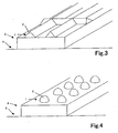
- the pattern shape of the recess-and-projection pattern 1 is any shape of the stripe shape such as FIG. 2 , the mesh shape such as FIGS. 1 and 3 , the honeycomb shape, and the point shape such as FIG.4 , the solder flow between the recesses and projections, and the contact area of both sides increases, and the electrode and the solder can be firmly adhered.
- the interval between the projections 2 among the recesses and projections is preferably set between 50 ⁇ m and 1 mm. This allows the contact area to increase, and the solder can surely flow between the recesses and projections of the electrode surface. This surely improves the adhesive strength, and can exert an anchor effect.
- FIGS.1 to 4 show the case where the pattern shape of the recess-and-projection pattern 1 is formed by the projection 2, if the solder can surely flow between the recesses and projections of the surface of the electrode, not necessarily by the projection 2, but by the recess, the stripe shape, the mesh shape, the honeycomb shape, and the point shape may be formed.
- the shape is the mesh shape such as FIGS. 1 and 3 or the honeycomb shape
- the difference in the directional character of the difficulty to peel off the connector can be eliminated, and when the projection 2 is formed by the point shape, a quantity consumed of the electrode material can be reduced.
- the shape of the projection or the recess formed in the point shape may be circle, oval, polygonal or asteroid.
- the bus bar electrode 3 comprises two layers. As a result, on the basis of at least one layer of the two layers of the bus electrode 3, the pattern shape of the recess-and-projection pattern 1 can be easily formed.
- the bus bar electrode 3 of the two-layered structure is formed, and by at least one printing and firing from among the two printings and firing, the recess-and-projection pattern 1 is preferably formed on the surface of the bus bar electrode 3 of the two-layered structure.
- a combination of the printing shapes includes, for example, the following three types.
- the first layer is printed in the flat shape like (1), and on top of that layer, the second layer is printed in the stripe shape like FIG.2 , and the second layer is printed in the mesh shape and the point shape like FIGS. 1 , 3, and 4 .
- the recess-and-projection pattern 1 can be surely formed on the bus bar electrode 3.
- the first layer is printed in the stripe shape, the mesh shape, the honeycomb shape, and the point shape, and on top of the first layer, the second layer is printed in the flat shape, so that the recess-and-projection pattern may be formed, and in this case, the second layer can be prevented from being peeled off from the first layer.
- the first layer and the second layer are not formed in the flat shape, respectively, but as a result of being superposed with each other, the recess-and-projection pattern can be also formed on the surface of the bus bar electrode 3.
- the connector to be soldered may be a connector that directly takes out the power from one piece of the solar cell or an inter-connector that takes out the power by mutually connecting a plurality of solar cells.
- a p-type single crystal solar cell silicon substrate (100 mm square, plane direction ⁇ 100 ⁇ , substrate thickness 300 ⁇ m, resistivity 0.5 ⁇ cm) doped with a group III element gallium as an impurity element was etched by potassium hydrate aqueous solution, thereby removing a damage layer. Further, by potassium hydrate aqueous solution mixed with IPA, a texture structure serving as an anti-reflection structure was formed.
- an n-region doped with phosphorus of a group V element as impurity was fabricated on the light receiving surface.
- the nitride film of 70 nm in thickness was formed on the light receiving surface by a plasma CVD method.
- the conductive paste containing aluminum particles was printed on the whole surface.
- the conductive paste containing silver particles was printed in the shapes of the finger electrode and the bus bar electrode, and was fired for three minutes at 700°C, thereby completing the solar cell.
- the bus bar electrode was printed twice to be superposed.
- the first layer (together with the finger electrode) was printed in the flat shape, and the second layer was printed in the mesh shape like FIGS. 1 and 3 (example).
- the width of the bus bar electrode was 1.5 mm, and the electrode thickness of the first layer was defined as 20 ⁇ m, and the electrode thickness of the second layer was defined as 30 ⁇ m (which becomes the recess-and-projection difference).
- the meshed line width of the second layer was 100 ⁇ m, and the interval of the lines was defined as 200 ⁇ m.
- the solar cell fabricated in the flat shape was prepared for the second layer, similar to the first layer (comparative example).
- the inter-connector was soldered on the bus bar, and a peeling probability when the inter-connector was pulled in the normal direction of the substrate surface by a force of 2 N was measured.
- the solar cell of the present invention having no need to enlarge the electrode width of the bus bar electrode has the shielding of the sunlight not enlarged and it is hardly affected in its efficiency.
- the present invention is not limited to the embodiment.
- the embodiment is illustrative, and has substantially the same configuration as the technical idea disclosed in the scope of the claims of the present invention, and any configuration exerting the same operational effect is contained in the technical scope of the present invention.
- the present invention is not limited thereto, and the fact that the connector soldered to the bus bar electrode easily peels off is also observed when the electrode is formed by vacuum deposition and the like, and needless to mention, an incidence rate of the peeling off can be reduced by the anchor effect through the application of the present invention.
- the electrode may be formed on both surfaces, and the present invention may be applied not only on the light receiving surface, but also on the bus bar electrode of the back surface, and can exert the effect.
Applications Claiming Priority (2)
| Application Number | Priority Date | Filing Date | Title |
|---|---|---|---|
| JP2005161251A JP2006339342A (ja) | 2005-06-01 | 2005-06-01 | 太陽電池および太陽電池の製造方法 |
| PCT/JP2006/309073 WO2006129446A1 (ja) | 2005-06-01 | 2006-05-01 | 太陽電池および太陽電池の製造方法 |
Publications (4)
| Publication Number | Publication Date |
|---|---|
| EP1887633A1 EP1887633A1 (en) | 2008-02-13 |
| EP1887633A4 EP1887633A4 (en) | 2008-10-22 |
| EP1887633B1 EP1887633B1 (en) | 2011-08-10 |
| EP1887633B2 true EP1887633B2 (en) | 2016-06-22 |
Family
ID=37481378
Family Applications (1)
| Application Number | Title | Priority Date | Filing Date |
|---|---|---|---|
| EP06745924.8A Active EP1887633B2 (en) | 2005-06-01 | 2006-05-01 | Solar cell and solar cell manufacturing method |
Country Status (10)
| Country | Link |
|---|---|
| US (1) | US20090025782A1 (zh) |
| EP (1) | EP1887633B2 (zh) |
| JP (1) | JP2006339342A (zh) |
| KR (1) | KR101258968B1 (zh) |
| CN (1) | CN101185170A (zh) |
| AU (1) | AU2006253714B2 (zh) |
| ES (1) | ES2369989T5 (zh) |
| RU (1) | RU2007144052A (zh) |
| TW (1) | TWI422047B (zh) |
| WO (1) | WO2006129446A1 (zh) |
Families Citing this family (33)
| Publication number | Priority date | Publication date | Assignee | Title |
|---|---|---|---|---|
| KR101108862B1 (ko) * | 2007-09-26 | 2012-01-31 | 히다치 가세고교 가부시끼가이샤 | 도전체 접속용 부재 및 그의 제조 방법, 접속 구조, 및 태양 전지 모듈 |
| TW200926210A (en) * | 2007-09-27 | 2009-06-16 | Murata Manufacturing Co | Ag electrode paste, solar battery cell, and process for producing the solar battery cell |
| KR100974221B1 (ko) * | 2008-04-17 | 2010-08-06 | 엘지전자 주식회사 | 레이저 어닐링을 이용한 태양전지의 선택적 에미터형성방법 및 이를 이용한 태양전지의 제조방법 |
| JP2009272406A (ja) * | 2008-05-02 | 2009-11-19 | Mitsubishi Electric Corp | 太陽電池素子 |
| JP2010034500A (ja) * | 2008-06-27 | 2010-02-12 | Kyocera Corp | 太陽電池モジュール |
| JP5368022B2 (ja) * | 2008-07-17 | 2013-12-18 | 信越化学工業株式会社 | 太陽電池 |
| DE102008036837A1 (de) * | 2008-08-07 | 2010-02-18 | Epcos Ag | Sensorvorrichtung und Verfahren zur Herstellung |
| JP2010073938A (ja) * | 2008-09-19 | 2010-04-02 | Sanyo Electric Co Ltd | 太陽電池モジュール及びその製造方法 |
| KR101133028B1 (ko) * | 2008-11-18 | 2012-04-04 | 에스에스씨피 주식회사 | 태양 전지용 전극의 제조방법, 이를 이용하여 제조된 태양 전지용 기판 및 태양 전지 |
| JP5306112B2 (ja) * | 2009-02-17 | 2013-10-02 | 三洋電機株式会社 | 太陽電池及び太陽電池モジュール |
| KR101135591B1 (ko) * | 2009-03-11 | 2012-04-19 | 엘지전자 주식회사 | 태양 전지 및 태양 전지 모듈 |
| EP2299501A1 (en) * | 2009-09-16 | 2011-03-23 | 3S Industries AG | Method and apparatus for providing a solar cell with a solder ribbon |
| KR101146734B1 (ko) * | 2009-10-26 | 2012-05-17 | 엘지전자 주식회사 | 태양 전지 셀 및 이를 구비한 태양 전지 모듈 |
| DE102010001780A1 (de) * | 2010-02-10 | 2011-08-11 | Koenen GmbH, 85521 | Solarzelle, Verfahren zur Herstellung einer Solarzelle und Druckschablone zum Aufbringen einer Kontaktierung einer Solarzelle |
| JP5312375B2 (ja) * | 2010-02-26 | 2013-10-09 | 三洋電機株式会社 | 太陽電池モジュール |
| DE102010016771B4 (de) * | 2010-05-04 | 2017-08-24 | Solarworld Innovations Gmbh | Verfahren zum Fixieren eines Photovoltaik-Zellenverbinders auf einer Oberfläche einer Photovoltaik-Zelle |
| US8525369B2 (en) | 2010-06-02 | 2013-09-03 | GM Global Technology Operations LLC | Method and device for optimizing the use of solar electrical power |
| RU2570814C2 (ru) * | 2010-12-24 | 2015-12-10 | Син-Эцу Кемикал Ко., Лтд. | Способ изготовления солнечного элемента и солнечный элемент |
| KR101275576B1 (ko) * | 2010-12-28 | 2013-06-14 | 엘지전자 주식회사 | 태양전지 및 이의 제조 방법 |
| JP2012138545A (ja) * | 2010-12-28 | 2012-07-19 | Sanyo Electric Co Ltd | 太陽電池セル及び太陽電池モジュール |
| US8691326B2 (en) * | 2011-04-01 | 2014-04-08 | E. I. Du Pont De Nemours And Company | Method for manufacturing solar cell electrode |
| WO2013046324A1 (ja) * | 2011-09-27 | 2013-04-04 | 三洋電機株式会社 | 太陽電池および太陽電池モジュール |
| JP5516566B2 (ja) * | 2011-12-19 | 2014-06-11 | 三洋電機株式会社 | 太陽電池モジュール及びその製造方法 |
| CN104040727B (zh) * | 2011-12-30 | 2016-07-06 | Memc新加坡私人有限公司 | 用于太阳能组件的汇流条 |
| US8636198B1 (en) * | 2012-09-28 | 2014-01-28 | Sunpower Corporation | Methods and structures for forming and improving solder joint thickness and planarity control features for solar cells |
| CN103178133A (zh) * | 2012-12-12 | 2013-06-26 | 英利能源(中国)有限公司 | 一种晶体硅太阳电池电极栅线结构 |
| US9837559B2 (en) | 2013-03-13 | 2017-12-05 | China Sunergy (Nanjing) Co. Ltd. | Soldering system |
| JP6064769B2 (ja) * | 2013-04-23 | 2017-01-25 | 三菱電機株式会社 | 太陽電池モジュール及び太陽電池セル |
| JP6630489B2 (ja) * | 2015-04-22 | 2020-01-15 | 矢崎総業株式会社 | 電子部品ユニット及びワイヤハーネス |
| US10490675B2 (en) | 2016-03-01 | 2019-11-26 | International Business Machines Corporation | User-preference driven control of electrical and thermal output from a photonic energy device |
| TWI590475B (zh) * | 2016-06-17 | 2017-07-01 | 財團法人工業技術研究院 | 堆疊型太陽能電池模組 |
| TWM539701U (zh) * | 2016-08-24 | 2017-04-11 | 新日光能源科技股份有限公司 | 太陽能電池 |
| US10280572B1 (en) * | 2017-11-07 | 2019-05-07 | Caterpillar Paving Products Inc. | System for heating a paving screed |
Family Cites Families (18)
| Publication number | Priority date | Publication date | Assignee | Title |
|---|---|---|---|---|
| JPH02235379A (ja) * | 1989-03-08 | 1990-09-18 | Mitsubishi Electric Corp | 太陽電池モジュール |
| US5118362A (en) * | 1990-09-24 | 1992-06-02 | Mobil Solar Energy Corporation | Electrical contacts and methods of manufacturing same |
| JP3077316B2 (ja) * | 1991-10-30 | 2000-08-14 | 富士電機株式会社 | 集積回路装置 |
| US5356488A (en) * | 1991-12-27 | 1994-10-18 | Rudolf Hezel | Solar cell and method for its manufacture |
| JP3442418B2 (ja) * | 1993-01-12 | 2003-09-02 | 三洋電機株式会社 | 光起電力素子 |
| JPH06318723A (ja) * | 1993-05-07 | 1994-11-15 | Canon Inc | 光起電力素子およびその作製方法 |
| US6265652B1 (en) * | 1995-06-15 | 2001-07-24 | Kanegafuchi Kagaku Kogyo Kabushiki Kabushiki Kaisha | Integrated thin-film solar battery and method of manufacturing the same |
| JP3653800B2 (ja) * | 1995-06-15 | 2005-06-02 | 株式会社カネカ | 集積化薄膜太陽電池の製造方法 |
| JPH09260696A (ja) * | 1996-03-19 | 1997-10-03 | Daido Hoxan Inc | 太陽電池 |
| JP3687236B2 (ja) * | 1996-12-03 | 2005-08-24 | 富士電機ホールディングス株式会社 | 薄膜光電変換素子 |
| JPH11121458A (ja) * | 1997-10-21 | 1999-04-30 | Nec Kyushu Ltd | 半導体装置 |
| JPH11307792A (ja) * | 1998-04-27 | 1999-11-05 | Kyocera Corp | 太陽電池素子 |
| JP3556112B2 (ja) | 1998-12-24 | 2004-08-18 | シャープ株式会社 | 太陽電池及びその製造方法 |
| JP2003142703A (ja) * | 2001-11-06 | 2003-05-16 | Sony Corp | 集積型太陽電池の製造方法 |
| AU2002367723A1 (en) * | 2002-02-28 | 2003-09-09 | Shin-Etsu Chemical Co., Ltd. | Solar cell module and manufacturing method thereof |
| JP4248356B2 (ja) * | 2003-09-26 | 2009-04-02 | 三洋電機株式会社 | 太陽電池装置および太陽電池モジュール |
| JP4232597B2 (ja) * | 2003-10-10 | 2009-03-04 | 株式会社日立製作所 | シリコン太陽電池セルとその製造方法 |
| TWI230427B (en) * | 2004-06-30 | 2005-04-01 | Phoenix Prec Technology Corp | Semiconductor device with electrical connection structure and method for fabricating the same |
-
2005
- 2005-06-01 JP JP2005161251A patent/JP2006339342A/ja active Pending
-
2006
- 2006-05-01 EP EP06745924.8A patent/EP1887633B2/en active Active
- 2006-05-01 CN CNA2006800189784A patent/CN101185170A/zh active Pending
- 2006-05-01 ES ES06745924.8T patent/ES2369989T5/es active Active
- 2006-05-01 AU AU2006253714A patent/AU2006253714B2/en not_active Ceased
- 2006-05-01 RU RU2007144052/28A patent/RU2007144052A/ru unknown
- 2006-05-01 US US11/919,999 patent/US20090025782A1/en not_active Abandoned
- 2006-05-01 WO PCT/JP2006/309073 patent/WO2006129446A1/ja active Application Filing
- 2006-05-01 KR KR1020077027657A patent/KR101258968B1/ko active IP Right Grant
- 2006-05-09 TW TW095116471A patent/TWI422047B/zh active
Also Published As
| Publication number | Publication date |
|---|---|
| EP1887633A4 (en) | 2008-10-22 |
| AU2006253714B2 (en) | 2011-06-30 |
| TWI422047B (zh) | 2014-01-01 |
| RU2007144052A (ru) | 2009-07-20 |
| CN101185170A (zh) | 2008-05-21 |
| KR20080018873A (ko) | 2008-02-28 |
| KR101258968B1 (ko) | 2013-04-29 |
| EP1887633A1 (en) | 2008-02-13 |
| ES2369989T3 (es) | 2011-12-09 |
| ES2369989T5 (es) | 2016-09-29 |
| JP2006339342A (ja) | 2006-12-14 |
| EP1887633B1 (en) | 2011-08-10 |
| WO2006129446A1 (ja) | 2006-12-07 |
| US20090025782A1 (en) | 2009-01-29 |
| AU2006253714A1 (en) | 2006-12-07 |
| TW200705697A (en) | 2007-02-01 |
Similar Documents
| Publication | Publication Date | Title |
|---|---|---|
| EP1887633B2 (en) | Solar cell and solar cell manufacturing method | |
| AU2017378670B2 (en) | Solar laminated cell inter-slice connection structure and solar laminated cell | |
| JP4738149B2 (ja) | 太陽電池モジュール | |
| EP1870942B1 (en) | Solar cell | |
| US20070209697A1 (en) | Solar Cell And Manufacturing Method Therefor | |
| EP3203530A1 (en) | Solar cell and method for manufacturing same | |
| EP2214214A1 (en) | Photoelectric conversion element and method for manufacturing the same | |
| WO2010095634A1 (ja) | 太陽電池モジュール | |
| WO2011162203A1 (ja) | 太陽電池 | |
| US20230044021A1 (en) | Solar cells having junctions retracted from cleaved edges | |
| JP2013030665A (ja) | 光電変換装置モジュール、光電変換装置モジュールの製造方法、及び光電変換装置 | |
| KR101192345B1 (ko) | 태양전지의 전극 패턴 및 이를 포함하는 태양전지 | |
| WO2013094556A1 (ja) | 配線シート付き太陽電池セル、太陽電池モジュールおよび太陽電池セルの製造方法 | |
| JP2005353851A (ja) | 太陽電池モジュール | |
| JP2003224289A (ja) | 太陽電池、太陽電池の接続方法、及び太陽電池モジュール | |
| CN112673481A (zh) | 具有环绕式指状物的太阳能电池 | |
| EP3984069A1 (en) | Optimised solar cell, solar cell module and method of manufacturing thereof | |
| JPH11266029A (ja) | 太陽電池及びその製造方法及びその接続方法 | |
| JP2007266649A (ja) | 太陽電池素子の製造方法 | |
| JP2011138922A (ja) | 太陽電池及び太陽電池製造用スクリーン製版 | |
| JP5858025B2 (ja) | 太陽電池の製造方法 | |
| US20150207019A1 (en) | Method for Fabricating Crystalline Silicon Solar Cell Having Passivation Layer and Local Rear Contacts | |
| KR20220005605A (ko) | 슁글드 고출력 모듈 및 그 제조방법 |
Legal Events
| Date | Code | Title | Description |
|---|---|---|---|
| PUAI | Public reference made under article 153(3) epc to a published international application that has entered the european phase |
Free format text: ORIGINAL CODE: 0009012 |
|
| 17P | Request for examination filed |
Effective date: 20071127 |
|
| AK | Designated contracting states |
Kind code of ref document: A1 Designated state(s): DE ES FR GB IT NL |
|
| RBV | Designated contracting states (corrected) |
Designated state(s): DE ES FR GB IT NL |
|
| DAX | Request for extension of the european patent (deleted) | ||
| A4 | Supplementary search report drawn up and despatched |
Effective date: 20080924 |
|
| RIC1 | Information provided on ipc code assigned before grant |
Ipc: H01L 31/0224 20060101AFI20080918BHEP |
|
| GRAP | Despatch of communication of intention to grant a patent |
Free format text: ORIGINAL CODE: EPIDOSNIGR1 |
|
| GRAS | Grant fee paid |
Free format text: ORIGINAL CODE: EPIDOSNIGR3 |
|
| GRAA | (expected) grant |
Free format text: ORIGINAL CODE: 0009210 |
|
| AK | Designated contracting states |
Kind code of ref document: B1 Designated state(s): DE ES FR GB IT NL |
|
| REG | Reference to a national code |
Ref country code: GB Ref legal event code: FG4D |
|
| REG | Reference to a national code |
Ref country code: DE Ref legal event code: R096 Ref document number: 602006023685 Country of ref document: DE Effective date: 20111006 |
|
| REG | Reference to a national code |
Ref country code: NL Ref legal event code: T3 |
|
| REG | Reference to a national code |
Ref country code: ES Ref legal event code: FG2A Ref document number: 2369989 Country of ref document: ES Kind code of ref document: T3 Effective date: 20111209 |
|
| PLBI | Opposition filed |
Free format text: ORIGINAL CODE: 0009260 |
|
| PLAX | Notice of opposition and request to file observation + time limit sent |
Free format text: ORIGINAL CODE: EPIDOSNOBS2 |
|
| 26 | Opposition filed |
Opponent name: PATENTANWAELTE BUSE MENTZEL LUDEWIG Effective date: 20120510 |
|
| REG | Reference to a national code |
Ref country code: DE Ref legal event code: R026 Ref document number: 602006023685 Country of ref document: DE Effective date: 20120510 |
|
| PLBB | Reply of patent proprietor to notice(s) of opposition received |
Free format text: ORIGINAL CODE: EPIDOSNOBS3 |
|
| REG | Reference to a national code |
Ref country code: FR Ref legal event code: PLFP Year of fee payment: 10 |
|
| RAP2 | Party data changed (patent owner data changed or rights of a patent transferred) |
Owner name: SHIN-ETSU HANDOTAI CO., LTD. Owner name: SHIN-ETSU CHEMICAL COMPANY, LTD. |
|
| REG | Reference to a national code |
Ref country code: FR Ref legal event code: PLFP Year of fee payment: 11 |
|
| PUAH | Patent maintained in amended form |
Free format text: ORIGINAL CODE: 0009272 |
|
| STAA | Information on the status of an ep patent application or granted ep patent |
Free format text: STATUS: PATENT MAINTAINED AS AMENDED |
|
| 27A | Patent maintained in amended form |
Effective date: 20160622 |
|
| AK | Designated contracting states |
Kind code of ref document: B2 Designated state(s): DE ES FR GB IT NL |
|
| REG | Reference to a national code |
Ref country code: DE Ref legal event code: R102 Ref document number: 602006023685 Country of ref document: DE |
|
| REG | Reference to a national code |
Ref country code: NL Ref legal event code: FP |
|
| REG | Reference to a national code |
Ref country code: ES Ref legal event code: DC2A Ref document number: 2369989 Country of ref document: ES Kind code of ref document: T5 Effective date: 20160929 |
|
| REG | Reference to a national code |
Ref country code: FR Ref legal event code: PLFP Year of fee payment: 12 |
|
| REG | Reference to a national code |
Ref country code: FR Ref legal event code: PLFP Year of fee payment: 13 |
|
| PGFP | Annual fee paid to national office [announced via postgrant information from national office to epo] |
Ref country code: NL Payment date: 20190412 Year of fee payment: 14 |
|
| PGFP | Annual fee paid to national office [announced via postgrant information from national office to epo] |
Ref country code: ES Payment date: 20190620 Year of fee payment: 14 Ref country code: IT Payment date: 20190527 Year of fee payment: 14 |
|
| PGFP | Annual fee paid to national office [announced via postgrant information from national office to epo] |
Ref country code: FR Payment date: 20190410 Year of fee payment: 14 |
|
| PGFP | Annual fee paid to national office [announced via postgrant information from national office to epo] |
Ref country code: GB Payment date: 20190501 Year of fee payment: 14 |
|
| REG | Reference to a national code |
Ref country code: NL Ref legal event code: MM Effective date: 20200601 |
|
| PG25 | Lapsed in a contracting state [announced via postgrant information from national office to epo] |
Ref country code: NL Free format text: LAPSE BECAUSE OF NON-PAYMENT OF DUE FEES Effective date: 20200601 |
|
| GBPC | Gb: european patent ceased through non-payment of renewal fee |
Effective date: 20200501 |
|
| PG25 | Lapsed in a contracting state [announced via postgrant information from national office to epo] |
Ref country code: FR Free format text: LAPSE BECAUSE OF NON-PAYMENT OF DUE FEES Effective date: 20200531 Ref country code: GB Free format text: LAPSE BECAUSE OF NON-PAYMENT OF DUE FEES Effective date: 20200501 |
|
| PG25 | Lapsed in a contracting state [announced via postgrant information from national office to epo] |
Ref country code: IT Free format text: LAPSE BECAUSE OF NON-PAYMENT OF DUE FEES Effective date: 20200501 |
|
| PG25 | Lapsed in a contracting state [announced via postgrant information from national office to epo] |
Ref country code: ES Free format text: LAPSE BECAUSE OF NON-PAYMENT OF DUE FEES Effective date: 20200502 |
|
| PGFP | Annual fee paid to national office [announced via postgrant information from national office to epo] |
Ref country code: DE Payment date: 20230331 Year of fee payment: 18 |