EP1810302B1 - Resistor having a predetermined temperature coefficient - Google Patents
Resistor having a predetermined temperature coefficient Download PDFInfo
- Publication number
- EP1810302B1 EP1810302B1 EP05794713A EP05794713A EP1810302B1 EP 1810302 B1 EP1810302 B1 EP 1810302B1 EP 05794713 A EP05794713 A EP 05794713A EP 05794713 A EP05794713 A EP 05794713A EP 1810302 B1 EP1810302 B1 EP 1810302B1
- Authority
- EP
- European Patent Office
- Prior art keywords
- magnetic field
- same
- layer
- circuit
- material stack
- Prior art date
- Legal status (The legal status is an assumption and is not a legal conclusion. Google has not performed a legal analysis and makes no representation as to the accuracy of the status listed.)
- Expired - Lifetime
Links
Images

Classifications
-
- B—PERFORMING OPERATIONS; TRANSPORTING
- B82—NANOTECHNOLOGY
- B82Y—SPECIFIC USES OR APPLICATIONS OF NANOSTRUCTURES; MEASUREMENT OR ANALYSIS OF NANOSTRUCTURES; MANUFACTURE OR TREATMENT OF NANOSTRUCTURES
- B82Y25/00—Nanomagnetism, e.g. magnetoimpedance, anisotropic magnetoresistance, giant magnetoresistance or tunneling magnetoresistance
-
- G—PHYSICS
- G01—MEASURING; TESTING
- G01R—MEASURING ELECTRIC VARIABLES; MEASURING MAGNETIC VARIABLES
- G01R33/00—Arrangements or instruments for measuring magnetic variables
- G01R33/02—Measuring direction or magnitude of magnetic fields or magnetic flux
- G01R33/06—Measuring direction or magnitude of magnetic fields or magnetic flux using galvano-magnetic devices
- G01R33/09—Magnetoresistive devices
- G01R33/093—Magnetoresistive devices using multilayer structures, e.g. giant magnetoresistance sensors
-
- H—ELECTRICITY
- H01—ELECTRIC ELEMENTS
- H01C—RESISTORS
- H01C7/00—Non-adjustable resistors formed as one or more layers or coatings; Non-adjustable resistors made from powdered conducting material or powdered semi-conducting material with or without insulating material
- H01C7/006—Thin film resistors
-
- H—ELECTRICITY
- H01—ELECTRIC ELEMENTS
- H01C—RESISTORS
- H01C7/00—Non-adjustable resistors formed as one or more layers or coatings; Non-adjustable resistors made from powdered conducting material or powdered semi-conducting material with or without insulating material
- H01C7/06—Non-adjustable resistors formed as one or more layers or coatings; Non-adjustable resistors made from powdered conducting material or powdered semi-conducting material with or without insulating material including means to minimise changes in resistance with changes in temperature
-
- H—ELECTRICITY
- H01—ELECTRIC ELEMENTS
- H01F—MAGNETS; INDUCTANCES; TRANSFORMERS; SELECTION OF MATERIALS FOR THEIR MAGNETIC PROPERTIES
- H01F10/00—Thin magnetic films, e.g. of one-domain structure
- H01F10/32—Spin-exchange-coupled multilayers, e.g. nanostructured superlattices
- H01F10/324—Exchange coupling of magnetic film pairs via a very thin non-magnetic spacer, e.g. by exchange with conduction electrons of the spacer
- H01F10/3268—Exchange coupling of magnetic film pairs via a very thin non-magnetic spacer, e.g. by exchange with conduction electrons of the spacer the exchange coupling being asymmetric, e.g. by use of additional pinning, by using antiferromagnetic or ferromagnetic coupling interface, i.e. so-called spin-valve [SV] structure, e.g. NiFe/Cu/NiFe/FeMn
- H01F10/3272—Exchange coupling of magnetic film pairs via a very thin non-magnetic spacer, e.g. by exchange with conduction electrons of the spacer the exchange coupling being asymmetric, e.g. by use of additional pinning, by using antiferromagnetic or ferromagnetic coupling interface, i.e. so-called spin-valve [SV] structure, e.g. NiFe/Cu/NiFe/FeMn by use of anti-parallel coupled [APC] ferromagnetic layers, e.g. artificial ferrimagnets [AFI], artificial [AAF] or synthetic [SAF] anti-ferromagnets
-
- H—ELECTRICITY
- H10—SEMICONDUCTOR DEVICES; ELECTRIC SOLID-STATE DEVICES NOT OTHERWISE PROVIDED FOR
- H10B—ELECTRONIC MEMORY DEVICES
- H10B61/00—Magnetic memory devices, e.g. magnetoresistive RAM [MRAM] devices
-
- H—ELECTRICITY
- H10—SEMICONDUCTOR DEVICES; ELECTRIC SOLID-STATE DEVICES NOT OTHERWISE PROVIDED FOR
- H10N—ELECTRIC SOLID-STATE DEVICES NOT OTHERWISE PROVIDED FOR
- H10N59/00—Integrated devices, or assemblies of multiple devices, comprising at least one galvanomagnetic or Hall-effect element covered by groups H10N50/00 - H10N52/00
-
- G—PHYSICS
- G01—MEASURING; TESTING
- G01R—MEASURING ELECTRIC VARIABLES; MEASURING MAGNETIC VARIABLES
- G01R15/00—Details of measuring arrangements of the types provided for in groups G01R17/00 - G01R29/00, G01R33/00 - G01R33/26 or G01R35/00
- G01R15/14—Adaptations providing voltage or current isolation, e.g. for high-voltage or high-current networks
- G01R15/20—Adaptations providing voltage or current isolation, e.g. for high-voltage or high-current networks using galvano-magnetic devices, e.g. Hall-effect devices, i.e. measuring a magnetic field via the interaction between a current and a magnetic field, e.g. magneto resistive or Hall effect devices
- G01R15/205—Adaptations providing voltage or current isolation, e.g. for high-voltage or high-current networks using galvano-magnetic devices, e.g. Hall-effect devices, i.e. measuring a magnetic field via the interaction between a current and a magnetic field, e.g. magneto resistive or Hall effect devices using magneto-resistance devices, e.g. field plates
Definitions
- This invention relates generally to electrical resistors and, in particular, to an electrical resistor having a predetermined temperature coefficient selected in accordance with a temperature coefficient of a magnetoresistance element.
- Magnetoresistance elements are known to be manufactured in a variety of configurations, including, but not limited to giant magnetoresistance (GMR) elements, and anisotropic magnetoresistance (AMR) elements.
- GMR giant magnetoresistance
- AMR anisotropic magnetoresistance
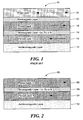
- a prior art GMR element 10 is formed having a plurality of layers, including an antiferromagnetic layer 12, a first pinned layer 14, a first non-magnetic layer 16, a second pinned layer 18, a second non-magnetic layer 20, and a free layer 22.
- the antiferromagnetic layer 12 comprises PtMn
- the first and second pinned layers 14, 18 are comprised of CoFe
- the first and second non-magnetic layers 16, 20 are comprised of a selected one of Ir and Ru
- the free layer 22 is comprised of NiFe.
- the antiferromagnetic layer 12 comprises PtMn
- the first and second pinned layers 14, 18 are comprised of CoFe
- the first and second non-magnetic layers 16, 20 are comprised of a selected one of Ir and Ru
- the free layer 22 is comprised of NiFe.
- other layers and materials can be provided in a GMR element.
- the magnetoresistance element is used in a variety of applications, including, but not limited to current sensors responsive to an electrical current, proximity detectors responsive to proximity of a ferromagnetic object, for example, ferrous gear teeth, and magnetic field sensors responsive to a magnetic field external to the magnetic field sensor.
- one or more magnetoresistance elements can be coupled either in a simple resistor divider or in a Wheatstone bridge arrangement.
- one or more fixed resistors can also be used along with the one or more magnetoresistance elements.
- the resistor divider and the Wheatstone bridge arrangement each provide an output voltage signal proportional to a magnetic field experienced by the one or more magnetoresistance elements.
- the magnetoresistance element has an electrical resistance that changes generally in proportion to a magnetic field in a direction of a maximum response axis of the magnetoresistance element.
- the electrical resistance changes not only in proportion to the magnetic field, but also in proportion to a temperature of the magnetoresistance element.
- the affect of temperature can be characterized as a temperature coefficient in units of resistance per degree temperature.
- the temperature coefficient of the magnetoresistance element when used in a resistor divider or in a Wheatstone bridge arrangement, can adversely affect the expected output voltage signal of the resistor divider or the Wheatstone bridge.
- the one or more resistors used in conjunction with the one or more magnetoresistance elements do not have the same temperature coefficient as the one or more magnetoresistance elements, then the output voltage signal of the resistor divider and the Wheatstone bridge arrangement will be responsive not only to a magnetic field, but also to temperature changes.
- An open loop arrangement of a current sensor, a proximity detector, or a magnetic field sensor is a known circuit arrangement in which one or more magnetic field sensing elements are exposed to a magnetic field generated external to the circuit.
- a closed loop arrangement of a current sensor, a proximity detector, or a magnetic field sensor is a known circuit arrangement in which one or more magnetic field sensing elements are exposed to both a magnetic field generated external to the circuit and also to an opposing magnetic field generated by the circuit, so as to keep the resulting magnetic field in the vicinity of the one or more magnetic field sensing elements near zero.
- the closed loop arrangement has certain known advantages over the open loop arrangement, including, but not limited to, improved linearity. Conversely, the open loop arrangement has certain known advantages over the closed loop arrangement, including, but not limited to, improved response time.
- US 2002/180433 A1 discloses a method of orienting the axis of magnetization of a first magnetic element with respect to a second magnetic element on a substrate, each of the magnetic elements having a first magnetic layer with an axis of magnetisation, the method including the step of depositing a pattern of flux-concentrating means close to the first magnetic element and subsequently orienting the axis of magnetisation of the first magnetic element in an applied magnetic field.
- Each of the magnetic elements contains a first magnetic layer having an axis of magnetization, a non-magnetic spacer layer, and a ferromagnetic layer as a free layer.
- the present invention provides a material stock as claimed in claim 1.
- the present invention provides a material stack forming a resistor having a temperature coefficient the same as or similar to the temperature coefficient of a giant magnetoresistance (GMR) element.
- GMR giant magnetoresistance
- a material stack includes an antiferromagnetic layer, a first pinned layer disposed over the antiferromagnetic layer, a non-magnetic layer disposed over the pinned layer, and a second pinned layer disposed over the non-magnetic layer.
- the material stack has an electrical resistance generally the same in the presence of a magnetic field and in the presence of no magnetic field, and the electrical resistance has a temperature coefficient generally the same as a temperature coefficient of a magnetoresistance element.
- the material stack provides an electrical resistance generally the same as that of a magnetoresistance element even when exposed to temperature variations.
- a circuit in accordance with another aspect of the present invention, includes a magnetoresistance element such as a giant magnetoresistance element, and a material stack as described above.
- the circuit can be a voltage divider, a Wheatstone bridge arrangement, a current sensor responsive to an electrical current, a proximity detector responsive to proximity of a ferromagnetic object, and a magnetic field sensor responsive to magnetic fields external to the circuit.
- the circuit can provide an output signal responsive to a magnetic field but generally unresponsive to temperature changes.
- the term “disposed over” is used to refer to a relative placement, without suggesting a requirement for up or down orientation.
- a first layer in combination with a second layer disposed over the first layer is not meant to require that the second layer be above the first layer.
- the second layer can be either above or below the first layer.
- the term “disposed over” also does not suggest a requirement for physical contact. For example, the above-described first and second layers need not be touching.
- an exemplary resistor 50 having a predetermined temperature coefficient is provided as a material stack including an antiferromagnetic layer 52, a first pinned layer 54, a non-magnetic layer 56, and a second pinned layer 58.
- the antiferromagnetic layer 52 comprises PtMn
- the first and second pinned layers 54, 58 are comprised of CoFe
- the non-magnetic layer 56 comprises a selected one of Ir and Ru. It will be recognized that the resistor 50 has most of the layers of the magnetoresistance element 10 of FIG. 1 . However, the second non-magnetic layer 20 and the free layer 22 of FIG. 1 are not present in the resistor 50. Therefore, the resistor 50 is not responsive to a magnetic field.
- the resistor 50 has a temperature coefficient the same as or similar to the temperature coefficient of a magnetoresistance element such as the magnetoresistance element 10 of FIG. 1 .
- a non-magnetic layer (not shown) is provided on top of the second pinned layer 58.
- the resistor 50 may have a nominal resistance that is different than the nominal resistance of the magnetoresistance element 10 at any particular temperature, while having a temperature coefficient that is generally the same as that of the magnetoresistance element 10.
- the width and the depth of the resistor 50 can be made to be different than the width and depth of the magnetoresistance element 10 in order to achieve a nominal resistance that is generally the same as that of the magnetoresistance element, while also retaining a temperature coefficient that is generally the same as that of the magnetoresistance element 10.
- the width and the depth to the resistor 50 can be made to have any dimensions within manufacturing capabilities to achieve any desired resistance.
- the non-magnetic layer 56 can be comprised of a plurality of non-magnetic layers, each of the plurality of non-magnetic layers formed from the same or a different material.
- the term "non-magnetic layer” is used to refer to both a single non-magnetic layer and also to a plurality of non-magnetic layers.
- a second non-magnetic layer (not shown) can be provided adjacent to the second pinned layer 58.
- the second non-magnetic layer can be the same as or similar to the second non-magnetic layer 20 of FIG. 1 .
- other material stacks can be provided to match other GMR structures, other than the GMR element 10 of FIG. 1 , merely by eliminating the associated free layer from the GMR structure.
- one or more other layers can be interposed between the layers 52-58.
- a voltage divider circuit 70 includes a resistor 72 and a magnetoresistance element 74.
- the resistor 72 is provided as a material stack as shown, for example, as the resistor 50 of FIG. 2 .
- an output voltage, Vout, of the resistor divider 70 is generally not responsive to temperature. However, the output voltage, Vout, is responsive to a magnetic field in the vicinity of the magnetoresistance element 74.
- a Wheatstone bridge circuit 100 includes first and second resistors 102, 104, respectively and first and second magnetoresistance elements 106, 108, respectively.
- the first and second resistors 102, 104 are each provided as a respective material stack as shown, for example, as the resistor 50 of FIG. 2 .
- an output voltage difference between Vout+ and Vout- of the Wheatstone bridge circuit 100 is generally not responsive to temperature. However, the output voltage difference is responsive to a magnetic field in which the magnetoresistance elements 106, 108 are placed.
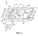
- the current sensor 150 contains first and second magnetoresistance elements 152, 155, respectively, and first and second resistors 168, 125, respectively.
- the resistors 168, 125 are each fabricated as a material stack in accordance with the resistor 50 of FIG. 2 .
- the magnetoresistance elements 152, 155 and resistors 168, 125 are disposed over a surface 154a of a silicon substrate 154.
- a secondary conductor 164 is also disposed over the surface 154a of the silicon substrate 154 proximate to the magnetoresistance elements 152, 155.
- a further, primary, conductor 158 is isolated from the silicon substrate 154 by a dielectric 156, as shown.
- a primary current 160 flows through the primary conductor 158, thereby generating a primary magnetic field 162.
- a secondary current 166 flows through the secondary conductor 164, thereby generating a secondary magnetic field 165 at the conductor portion 164a. Because the secondary current 166 passes through the secondary conductor portion 164a in a direction opposite to the primary current 160 passing through the primary conductor 158, the secondary magnetic field 165 is opposite in direction to the primary magnetic field 162.
- a first voltage source 174 here integrated in the silicon substrate 154, provides a current through the first resistor 168 and the first magnetoresistance element 152 and, therefore, generates a voltage at node 170 having a magnitude related to the magnetic field experienced by the first magnetoresistance element 152.
- a second voltage source 159 also here integrated in the silicon substrate 154, provides a current through the second magnetoresistance element 155 and the second resistor 125 and, therefore, generates a voltage at node 171 having a magnitude related to the magnetic field experienced by the second magnetoresistance element 155.
- the first and the second voltage sources 174, 159 supply the same voltage and are provided by a single voltage source.
- An amplifier 172 coupled to the nodes 170, 171, provides the secondary current 166 to the secondary conductor 164 in response to the voltage difference between the nodes 170 and 171.
- the first magnetoresistance element 152 has a response axis 153
- the second magnetoresistance element 155 has a response axis 157.
- the magnetoresistence elements 152,155 are polarized in the same direction.
- the secondary current 166 passes by the first and second magnetoresistance elements 152, 155 in the same direction. Therefore, when exposed to the secondary magnetic field 165 the voltages at nodes 170, 171 move in response to the magnetic field in opposite directions.
- the node 170 is coupled to a negative input of the amplifier 172 and the node 171 is coupled to a positive input of the amplifier 172.
- the amplifier 172 generates the secondary current 166 in proportion to the voltage difference between nodes 170 and 171.
- the voltage at the node 171 tends to increase in response to the primary magnetic field 162 and the voltage at the node 170 tends to decrease.
- the secondary magnetic field 165 tends to oppose the primary magnetic field 162.
- the magnetic field experienced by the first magnetoresistance element 152 is the sum of the secondary magnetic field 165 and the primary magnetic field 162 along the response axis 153.
- the magnetic field experienced by the second magnetoresistance element 155 is the sum of the secondary magnetic field 165 and the primary magnetic field 162 along the response axes 157. Since the secondary magnetic field 165 is opposite in direction to the primary magnetic field 162, the secondary magnetic field 165 tends to cancel the primary magnetic field 162.
- the amplifier 172 provides the secondary current 166 at a level necessary to generate the secondary magnetic field 165 sufficient to cancel the primary magnetic field 162 along the response axes 153, 157 so that the total magnetic field experienced by the first and second magnetoresistance elements 152, 155 is substantially zero gauss.
- the secondary current 166 passes through a resistor 176, thereby generating an output voltage, Vout, between output terminals 178, 180 in proportion to the secondary current 166.
- Vout is proportional to the secondary magnetic field 165, and is thus proportional to the primary current 160, as desired.
- the resistor 176 has a resistance with a temperature coefficient.
- One of ordinary skill in the art will recognize techniques that can be used to reduce the affect of this temperature coefficient. For example, an operational amplifier circuit with a properly matched feedback compensation network can be used reduce the affect:
- the two magnetoresistance elements 152, 155 and the two resistors 168, 125 provide a Wheatstone bridge circuit as shown, for example, in FIG. 4 . It should be appreciated that, since the resistors 168, 125 are provided as material stacks in accordance with the resistor 50 of FIG. 2 , having a temperature coefficient essentially the same as the temperature coefficients of the magnetoresistance elements 152, 155, the voltage difference between the nodes 170, 171 will be essentially unaffected by temperature changes, and therefore, the output voltage, Vout, will be similarly unaffected.
- closed loop current sensor 150 has two magnetoresistance elements 152, 155, and two resistors 168, 125
- alternative closed loop current sensors can be provided with more than two or fewer than two magnetoresistance elements and more than two or fewer than two resistors.
- the silicon substrate 154 is shown, it will also be apparent that other substrate materials, including but not limited to, SiGe, GaAs, or mGaAs can be used in place of the silicon substrate 154 without departing from the present invention.
- the silicon substrate 154 can be replaced by another substrate (not shown) comprised of a ceramic material, including but not limited to Al 2 O 3 ,
- a magnetoresistance element and a resistor formed as a material stack in accordance with the resistor 50 of FIG. 2 can be fabricated on the ceramic substrate.
- Circuitry similar to the amplifier 172 be formed, for example, on a separate substrate (not shown), for example, on a silicon substrate, which can be coupled with wire bonds or the like to the ceramic substrate.
- an electronic circuit 200 in the form of a magnetic field sensor includes a silicon substrate 204, first and second magnetoresistance elements 202, 205, respectively and first and second resistors 218, 215, respectively , disposed over a surface 204a of the silicon substrate 204.
- a conductor 214 is also disposed over the surface 204a of the silicon substrate 204 proximate to the magnetoresistance elements.
- the first and second resistors 218, 215 are provided as material stacks in accordance with the material stack 50 of FIG. 2 .
- the magnetic field sensor 200 is adapted to sense are external magnetic field 240 and to provide an output signal, Vout, proportional to the magnetic field 240.
- a current 216 flows through a first portion 214a of conductor 214, thereby generating a magnetic field 217.
- the magnetic field 217 is in the opposite direction with respect to the external magnetic field 240.
- the magnetic field 217 tends to cancel the external magnetic field 240.
- a first voltage source 224 here integrated in the silicon substrate 204, provides a current through the first resistor 218 and the first magnetoresistance element 202, and therefore, generates a voltage at node 220 having a magnitude related to the magnetic field experienced by the first magnetoresistance element 202.
- a second voltage source 209 also here integrated in the silicon substrate 204, provides a current through the second magnetoresistance element 205 and the second resistor 215, and therefore, generates a voltage at node 221 having a magnitude related to the magnetic field experienced by the second magnetoresistance element 205.
- the first and the second voltage sources 224, 209 supply the same voltage and are provided by a single voltage source.
- An amplifier 222 provides the secondary current 216 to the secondary conductor 214 in response to a voltage difference between the nodes 220 and 221.
- the first magnetoresistance element 202 has a response axis 203 and the second magnetoresistance element 205 has a response axis 207.
- the first and second magnetoresistance elements 202, 205 are polarized in the same direction.
- the current 216 passes by the first and second magnetoresistance elements 202, 205, in the same direction. Therefore, when exposed to the magnetic field 217, the voltage at the node 220 moves in one voltage direction and the voltage at the node 221 moves in the other voltage direction.
- the node 220 is coupled to a negative input of the amplifier 222 and the node 221 is coupled to a positive input of the amplifier 222.
- the voltage at the node 221 tends to increase while the voltage at the node 220 tends to decrease in response to the external magnetic field 240.
- the magnetic field 217 tends to oppose the external magnetic field 240.
- the first and second magnetoresistance elements 202, 205 are oriented such that the response axes 203, 207 are aligned with the external magnetic field 240 and also with the magnetic field 217.
- the magnetic field experienced by the first and second magnetoresistance elements 202, 205 is the sum of the magnetic field 217 and the external magnetic field 240 along the response axes 203, 207 respectively. Since the magnetic field 217 is opposite in direction to the external magnetic field 240 along the response axes 203, 207 the magnetic field 217 tends to cancel the external magnetic field 240.
- the amplifier 222 generates the current 216 in proportion to the voltage difference between the node 220 and the node 221.
- the amplifier 222 provides the current 216 at a level necessary to generate the magnetic field 217 sufficient to cancel the external magnetic field 240 along the response axes 203, 207 so that the total magnetic field experienced by each of the magnetoresistance elements 202, 205 is substantially zero gauss.
- the current 216 passes through a resistor 226 thereby generating an output voltage, Vout, between output terminals 228, 230 in proportion to the current 216.
- Vout is proportional to the magnetic field 217 necessary to cancel the external magnetic field 240, and is thus proportional to the external magnetic field 240, as desired.
- the two magnetoresistance elements 202, 205 and the two resistors 218, 215 provide a Wheatstone bridge circuit as shown, for example, in FIG. 4 . It should be appreciated that, since the resistors 218, 215 are provided as material stacks in accordance with the resistor 50 of FIG. 2 , having a temperature coefficient essentially the same as the temperature coefficients of the magnetoresistance elements 202, 205, the voltage difference between the nodes 220, 221 will be essentially unaffected by temperature changes, and therefore, the output voltage, Vout, will be similarly unaffected.
- closed loop magnetic field sensor 200 is shown having two magnetoresistance elements 202, 205 and two resistors 218, 215, in an alternate arrangement, a closed loop magnetic field sensor can have more than two or fewer than two magnetoresistance elements and more than two or fewer than two resistors.
- the silicon substrate 204 is shown, it will also be apparent that other substrate materials, including but not limited to, SiGe, GaAs, or InGaAs can be used in place of the silicon substrate 204 without departing from the present invention.
- the silicon substrate 204 can be replaced by another substrate (not shown) comprised of a ceramic material, including but not limited to AlO 3 .
- a magnetoresistance element and a resistor formed as a material stack in accordance with the resistor 50 of FIG. 2 can be fabricated on the ceramic substrate.
- Circuitry similar to the amplifier 222 can be formed, for example, on a separate substrate (not shown), for example, on a silicon substrate, which can be coupled with wire bonds or the like to the ceramic substrate.
- closed loop current sensor 150 is shown in FIG. 5 and a closed loop magnetic field sensor 200 is shown in FIG. 6
- open loop arrangements can be provided having resistors formed as material stacks in accordance with the material stack 50 of FIG. 2 .
- a proximity detector either closed loop or open loop, which is responsive to an external magnetic field generated, for example, by ferrous gear teeth, can also be provided having resistors formed as material stacks in accordance with the material stack 50 of FIG. 2 .
Landscapes
- Engineering & Computer Science (AREA)
- Physics & Mathematics (AREA)
- Microelectronics & Electronic Packaging (AREA)
- Chemical & Material Sciences (AREA)
- Electromagnetism (AREA)
- Crystallography & Structural Chemistry (AREA)
- Nanotechnology (AREA)
- General Physics & Mathematics (AREA)
- Condensed Matter Physics & Semiconductors (AREA)
- Power Engineering (AREA)
- Hall/Mr Elements (AREA)
- Measuring Magnetic Variables (AREA)
- Measuring Instrument Details And Bridges, And Automatic Balancing Devices (AREA)
- Semiconductor Integrated Circuits (AREA)
- Geophysics And Detection Of Objects (AREA)
Applications Claiming Priority (2)
| Application Number | Priority Date | Filing Date | Title |
|---|---|---|---|
| US10/962,889 US7777607B2 (en) | 2004-10-12 | 2004-10-12 | Resistor having a predetermined temperature coefficient |
| PCT/US2005/029982 WO2006044031A1 (en) | 2004-10-12 | 2005-08-22 | Resistor having a predetermined temperature coefficient |
Publications (2)
| Publication Number | Publication Date |
|---|---|
| EP1810302A1 EP1810302A1 (en) | 2007-07-25 |
| EP1810302B1 true EP1810302B1 (en) | 2012-03-28 |
Family
ID=35502739
Family Applications (1)
| Application Number | Title | Priority Date | Filing Date |
|---|---|---|---|
| EP05794713A Expired - Lifetime EP1810302B1 (en) | 2004-10-12 | 2005-08-22 | Resistor having a predetermined temperature coefficient |
Country Status (5)
| Country | Link |
|---|---|
| US (1) | US7777607B2 (enExample) |
| EP (1) | EP1810302B1 (enExample) |
| JP (3) | JP4722934B2 (enExample) |
| AT (1) | ATE551702T1 (enExample) |
| WO (1) | WO2006044031A1 (enExample) |
Families Citing this family (68)
| Publication number | Priority date | Publication date | Assignee | Title |
|---|---|---|---|---|
| US7259545B2 (en) | 2003-02-11 | 2007-08-21 | Allegro Microsystems, Inc. | Integrated sensor |
| US7777607B2 (en) | 2004-10-12 | 2010-08-17 | Allegro Microsystems, Inc. | Resistor having a predetermined temperature coefficient |
| US7768083B2 (en) | 2006-01-20 | 2010-08-03 | Allegro Microsystems, Inc. | Arrangements for an integrated sensor |
| US7573112B2 (en) * | 2006-04-14 | 2009-08-11 | Allegro Microsystems, Inc. | Methods and apparatus for sensor having capacitor on chip |
| US7687882B2 (en) * | 2006-04-14 | 2010-03-30 | Allegro Microsystems, Inc. | Methods and apparatus for integrated circuit having multiple dies with at least one on chip capacitor |
| US20080013298A1 (en) | 2006-07-14 | 2008-01-17 | Nirmal Sharma | Methods and apparatus for passive attachment of components for integrated circuits |
| JP5015966B2 (ja) * | 2007-02-02 | 2012-09-05 | アルプス電気株式会社 | 磁気検出装置及びその製造方法 |
| US7795862B2 (en) | 2007-10-22 | 2010-09-14 | Allegro Microsystems, Inc. | Matching of GMR sensors in a bridge |
| US9823090B2 (en) | 2014-10-31 | 2017-11-21 | Allegro Microsystems, Llc | Magnetic field sensor for sensing a movement of a target object |
| US7816905B2 (en) * | 2008-06-02 | 2010-10-19 | Allegro Microsystems, Inc. | Arrangements for a current sensing circuit and integrated current sensor |
| US8093670B2 (en) * | 2008-07-24 | 2012-01-10 | Allegro Microsystems, Inc. | Methods and apparatus for integrated circuit having on chip capacitor with eddy current reductions |
| US20100052424A1 (en) * | 2008-08-26 | 2010-03-04 | Taylor William P | Methods and apparatus for integrated circuit having integrated energy storage device |
| JP5250108B2 (ja) * | 2009-06-12 | 2013-07-31 | アルプス・グリーンデバイス株式会社 | 磁気平衡式電流センサ |
| JP5250109B2 (ja) | 2009-06-12 | 2013-07-31 | アルプス・グリーンデバイス株式会社 | 磁気平衡式電流センサ |
| JP4945606B2 (ja) * | 2009-07-24 | 2012-06-06 | 株式会社東芝 | 磁気抵抗効果素子,および磁気抵抗効果素子の製造方法 |
| WO2011043193A1 (ja) * | 2009-10-05 | 2011-04-14 | アルプス・グリーンデバイス株式会社 | 磁気平衡式電流センサ |
| US20110133732A1 (en) * | 2009-12-03 | 2011-06-09 | Allegro Microsystems, Inc. | Methods and apparatus for enhanced frequency response of magnetic sensors |
| WO2011111493A1 (ja) | 2010-03-12 | 2011-09-15 | アルプス・グリーンデバイス株式会社 | 電流センサ |
| WO2011111648A1 (ja) | 2010-03-12 | 2011-09-15 | アルプス電気株式会社 | 磁気センサ及びそれを用いた磁気平衡式電流センサ |
| WO2012026255A1 (ja) * | 2010-08-23 | 2012-03-01 | アルプス・グリーンデバイス株式会社 | 磁気平衡式電流センサ |
| JP5794777B2 (ja) | 2010-12-22 | 2015-10-14 | 三菱電機株式会社 | 半導体装置 |
| US8629539B2 (en) | 2012-01-16 | 2014-01-14 | Allegro Microsystems, Llc | Methods and apparatus for magnetic sensor having non-conductive die paddle |
| US10234513B2 (en) | 2012-03-20 | 2019-03-19 | Allegro Microsystems, Llc | Magnetic field sensor integrated circuit with integral ferromagnetic material |
| US9812588B2 (en) | 2012-03-20 | 2017-11-07 | Allegro Microsystems, Llc | Magnetic field sensor integrated circuit with integral ferromagnetic material |
| US9494660B2 (en) | 2012-03-20 | 2016-11-15 | Allegro Microsystems, Llc | Integrated circuit package having a split lead frame |
| US9666788B2 (en) | 2012-03-20 | 2017-05-30 | Allegro Microsystems, Llc | Integrated circuit package having a split lead frame |
| US9411025B2 (en) | 2013-04-26 | 2016-08-09 | Allegro Microsystems, Llc | Integrated circuit package having a split lead frame and a magnet |
| US9529060B2 (en) | 2014-01-09 | 2016-12-27 | Allegro Microsystems, Llc | Magnetoresistance element with improved response to magnetic fields |
| US9719806B2 (en) | 2014-10-31 | 2017-08-01 | Allegro Microsystems, Llc | Magnetic field sensor for sensing a movement of a ferromagnetic target object |
| JP6482023B2 (ja) * | 2015-05-22 | 2019-03-13 | アルプスアルパイン株式会社 | 磁気センサ |
| EP3300534B1 (en) | 2015-06-05 | 2020-11-11 | Allegro MicroSystems, LLC | Spin valve magnetoresistance element with improved response to magnetic fields |
| US10411498B2 (en) | 2015-10-21 | 2019-09-10 | Allegro Microsystems, Llc | Apparatus and methods for extending sensor integrated circuit operation through a power disturbance |
| US20170163065A1 (en) * | 2015-12-08 | 2017-06-08 | Benjamin Avery Freer | Constant power supply for thermo-electric cells |
| US10114085B2 (en) | 2016-03-04 | 2018-10-30 | Allegro Microsystems, Llc | Magnetic field sensor with improved response immunity |
| US9910087B2 (en) | 2016-03-14 | 2018-03-06 | Allegro Microsystems, Llc | Integrated circuit and method for detecting a stress condition in the integrated circuit |
| US10036785B2 (en) | 2016-07-18 | 2018-07-31 | Allegro Microsystems, Llc | Temperature-compensated magneto-resistive sensor |
| DE102017004349A1 (de) | 2017-05-08 | 2018-11-08 | Tdk-Micronas Gmbh | Magnetfeldkompensationseinrichtung |
| US10620279B2 (en) | 2017-05-19 | 2020-04-14 | Allegro Microsystems, Llc | Magnetoresistance element with increased operational range |
| US11022661B2 (en) | 2017-05-19 | 2021-06-01 | Allegro Microsystems, Llc | Magnetoresistance element with increased operational range |
| JP6658676B2 (ja) * | 2017-06-13 | 2020-03-04 | Tdk株式会社 | 電流センサ |
| US10768246B2 (en) * | 2017-09-21 | 2020-09-08 | Tdk Corporation | Magnetic sensor with elongated soft magnetic body |
| US10921373B2 (en) * | 2017-11-29 | 2021-02-16 | Allegro Microsystems, Llc | Magnetic field sensor able to identify an error condition |
| US11002806B2 (en) * | 2018-03-29 | 2021-05-11 | Asahi Kasei Microdevices Corporation | Magnetic field detection device |
| JP7232647B2 (ja) * | 2018-03-29 | 2023-03-03 | 旭化成エレクトロニクス株式会社 | 磁気検出装置 |
| US10978897B2 (en) | 2018-04-02 | 2021-04-13 | Allegro Microsystems, Llc | Systems and methods for suppressing undesirable voltage supply artifacts |
| US10605874B2 (en) | 2018-08-06 | 2020-03-31 | Allegro Microsystems, Llc | Magnetic field sensor with magnetoresistance elements having varying sensitivity |
| US10935612B2 (en) | 2018-08-20 | 2021-03-02 | Allegro Microsystems, Llc | Current sensor having multiple sensitivity ranges |
| US10991644B2 (en) | 2019-08-22 | 2021-04-27 | Allegro Microsystems, Llc | Integrated circuit package having a low profile |
| JP7140149B2 (ja) * | 2020-01-31 | 2022-09-21 | Tdk株式会社 | 電流センサ、磁気センサ及び回路 |
| US11385075B2 (en) | 2020-02-21 | 2022-07-12 | Allegro Microsystems, Llc | Orientation independent magnetic field sensor |
| US11163021B2 (en) | 2020-03-05 | 2021-11-02 | Allegro Microsystems, Llc | Sensors having signal redundancy |
| US11561112B2 (en) | 2020-03-13 | 2023-01-24 | Allegro Microsystems, Llc | Current sensor having stray field immunity |
| US11187764B2 (en) | 2020-03-20 | 2021-11-30 | Allegro Microsystems, Llc | Layout of magnetoresistance element |
| US11333718B2 (en) | 2020-04-15 | 2022-05-17 | Allegro Microsystems, Llc | Sensors having dynamic phase compensation |
| US11262422B2 (en) | 2020-05-08 | 2022-03-01 | Allegro Microsystems, Llc | Stray-field-immune coil-activated position sensor |
| US11275130B2 (en) * | 2020-06-25 | 2022-03-15 | Western Digital Technologies, Inc. | Magnetic sensor bridge using dual free layer |
| US11630168B2 (en) | 2021-02-03 | 2023-04-18 | Allegro Microsystems, Llc | Linear sensor with dual spin valve element having reference layers with magnetization directions different from an external magnetic field direction |
| US11493361B2 (en) | 2021-02-26 | 2022-11-08 | Allegro Microsystems, Llc | Stray field immune coil-activated sensor |
| US11567108B2 (en) | 2021-03-31 | 2023-01-31 | Allegro Microsystems, Llc | Multi-gain channels for multi-range sensor |
| EP4130772B1 (en) | 2021-08-05 | 2025-07-23 | Allegro MicroSystems, LLC | Magnetoresistive element having compensated temperature coefficient of tmr |
| US11994541B2 (en) | 2022-04-15 | 2024-05-28 | Allegro Microsystems, Llc | Current sensor assemblies for low currents |
| US11719771B1 (en) | 2022-06-02 | 2023-08-08 | Allegro Microsystems, Llc | Magnetoresistive sensor having seed layer hysteresis suppression |
| US12320870B2 (en) | 2022-07-19 | 2025-06-03 | Allegro Microsystems, Llc | Controlling out-of-plane anisotropy in an MR sensor with free layer dusting |
| US12359904B2 (en) | 2023-01-26 | 2025-07-15 | Allegro Microsystems, Llc | Method of manufacturing angle sensors including magnetoresistance elements including different types of antiferromagnetic materials |
| US12352832B2 (en) | 2023-01-30 | 2025-07-08 | Allegro Microsystems, Llc | Reducing angle error in angle sensor due to orthogonality drift over magnetic-field |
| US12140646B2 (en) | 2023-02-06 | 2024-11-12 | Allegro Microsystems, Llc | Magnetic sensing having hall plate routing to reduce inductive coupling |
| US12248039B2 (en) | 2023-08-08 | 2025-03-11 | Allegro Microsystems, Llc | Interleaving sub-arrays of magnetoresistance elements based on reference directions to compensate for bridge offset |
| US12467990B2 (en) | 2023-08-30 | 2025-11-11 | Allegro Microsystems, Llc | Magnetoresistance signal path compensation |
Family Cites Families (123)
| Publication number | Priority date | Publication date | Assignee | Title |
|---|---|---|---|---|
| US3858189A (en) * | 1972-12-29 | 1974-12-31 | Ibm | Magneto resistive signal multiplier for sensing magnetic bubble domains |
| US3860965A (en) * | 1973-10-04 | 1975-01-14 | Ibm | Magnetoresistive read head assembly having matched elements for common mode rejection |
| US4035785A (en) * | 1975-12-31 | 1977-07-12 | International Business Machines Corporation | Bubble domain sensor-error detector |
| US4078230A (en) * | 1976-02-02 | 1978-03-07 | Rockwell International Corporation | Multi-segment detector |
| US4159537A (en) * | 1978-05-01 | 1979-06-26 | Burroughs Corporation | Bubble detector-dynamic level signal shifting |
| US4343026A (en) * | 1980-07-09 | 1982-08-03 | Spin Physics, Inc. | Magnetoresistive head employing field feedback |
| CH651671A5 (de) * | 1980-12-24 | 1985-09-30 | Landis & Gyr Ag | Anordnung zur messung elektrischer leistung oder energie. |
| CH651701A5 (de) * | 1980-12-24 | 1985-09-30 | Landis & Gyr Ag | Kompensierter messwandler. |
| US4432069A (en) * | 1981-01-29 | 1984-02-14 | Intel Corporation | Multiplexed magnetic bubble detectors |
| DE3426784A1 (de) * | 1984-07-20 | 1986-01-30 | Bosch Gmbh Robert | Magnetoresistiver sensor zur abgabe von elektrischen signalen |
| CA1248222A (en) * | 1984-08-27 | 1989-01-03 | Yutaka Souda | Magnetic transducer head utilizing magnetoresistance effect |
| US4860432A (en) * | 1986-09-02 | 1989-08-29 | Alps Electric Co., Ltd. | Method of manufacturing a magnetoresistive sensor |
| CH669852A5 (enExample) * | 1986-12-12 | 1989-04-14 | Lem Liaisons Electron Mec | |
| KR910004261B1 (ko) * | 1987-04-09 | 1991-06-25 | 후지쓰 가부시끼가이샤 | 자전 변환 소자를 이용한 검지기 |
| EP0300635B1 (en) * | 1987-07-07 | 1995-09-13 | Nippondenso Co., Ltd. | Current detecting device using ferromagnetic magnetoresistance element |
| US4823075A (en) * | 1987-10-13 | 1989-04-18 | General Electric Company | Current sensor using hall-effect device with feedback |
| US4939459A (en) * | 1987-12-21 | 1990-07-03 | Tdk Corporation | High sensitivity magnetic sensor |
| US5227721A (en) * | 1987-12-25 | 1993-07-13 | Sharp Kabushiki Kaisha | Superconductive magnetic sensor having self induced magnetic biasing |
| US5041780A (en) * | 1988-09-13 | 1991-08-20 | California Institute Of Technology | Integrable current sensors |
| US4847584A (en) * | 1988-10-14 | 1989-07-11 | Honeywell Inc. | Magnetoresistive magnetic sensor |
| JPH02246176A (ja) * | 1989-03-17 | 1990-10-01 | Sanyo Electric Co Ltd | 磁気センサ |
| JPH05126865A (ja) | 1991-10-22 | 1993-05-21 | Hitachi Ltd | 電流検出装置あるいは電流検出方法 |
| DE4212737C1 (en) | 1992-04-16 | 1993-07-08 | Leica Mikroskopie Und Systeme Gmbh | Compact bridge-connected sensor - has thin-film resistors on substrate |
| US5260653A (en) * | 1992-06-03 | 1993-11-09 | Eastman Kodak Company | Thin film very high sensitivity magnetoresistive magnetometer having temperature compensation and simple domain stability |
| US5617071A (en) * | 1992-11-16 | 1997-04-01 | Nonvolatile Electronics, Incorporated | Magnetoresistive structure comprising ferromagnetic thin films and intermediate alloy layer having magnetic concentrator and shielding permeable masses |
| DE4243358A1 (de) * | 1992-12-21 | 1994-06-23 | Siemens Ag | Magnetowiderstands-Sensor mit künstlichem Antiferromagneten und Verfahren zu seiner Herstellung |
| DE4300605C2 (de) * | 1993-01-13 | 1994-12-15 | Lust Electronic Systeme Gmbh | Sensorchip |
| US6021065A (en) * | 1996-09-06 | 2000-02-01 | Nonvolatile Electronics Incorporated | Spin dependent tunneling memory |
| US6002553A (en) * | 1994-02-28 | 1999-12-14 | The United States Of America As Represented By The United States Department Of Energy | Giant magnetoresistive sensor |
| US5583725A (en) * | 1994-06-15 | 1996-12-10 | International Business Machines Corporation | Spin valve magnetoresistive sensor with self-pinned laminated layer and magnetic recording system using the sensor |
| US5500590A (en) * | 1994-07-20 | 1996-03-19 | Honeywell Inc. | Apparatus for sensing magnetic fields using a coupled film magnetoresistive transducer |
| DE4436876A1 (de) * | 1994-10-15 | 1996-04-18 | Lust Antriebstechnik Gmbh | Sensorchip |
| US5561368A (en) * | 1994-11-04 | 1996-10-01 | International Business Machines Corporation | Bridge circuit magnetic field sensor having spin valve magnetoresistive elements formed on common substrate |
| US5570034A (en) * | 1994-12-29 | 1996-10-29 | Intel Corporation | Using hall effect to monitor current during IDDQ testing of CMOS integrated circuits |
| US5929636A (en) * | 1996-05-02 | 1999-07-27 | Integrated Magnetoelectronics | All-metal giant magnetoresistive solid-state component |
| DE19619806A1 (de) * | 1996-05-15 | 1997-11-20 | Siemens Ag | Magnetfeldempfindliche Sensoreinrichtung mit mehreren GMR-Sensorelementen |
| US5831426A (en) * | 1996-08-16 | 1998-11-03 | Nonvolatile Electronics, Incorporated | Magnetic current sensor |
| DE19650078A1 (de) | 1996-12-03 | 1998-06-04 | Inst Mikrostrukturtechnologie | Sensorelement zur Bestimmung eines Magnetfeldes oder eines Stromes |
| US5877705A (en) * | 1997-04-22 | 1999-03-02 | Nu-Metrics, Inc. | Method and apparatus for analyzing traffic and a sensor therefor |
| EP0927361A1 (en) * | 1997-06-13 | 1999-07-07 | Koninklijke Philips Electronics N.V. | Sensor comprising a wheatstone bridge |
| US5952825A (en) * | 1997-08-14 | 1999-09-14 | Honeywell Inc. | Magnetic field sensing device having integral coils for producing magnetic fields |
| US6300617B1 (en) * | 1998-03-04 | 2001-10-09 | Nonvolatile Electronics, Incorporated | Magnetic digital signal coupler having selected/reversal directions of magnetization |
| JP3623366B2 (ja) * | 1998-07-17 | 2005-02-23 | アルプス電気株式会社 | 巨大磁気抵抗効果素子を備えた磁界センサおよびその製造方法と製造装置 |
| JP3623367B2 (ja) * | 1998-07-17 | 2005-02-23 | アルプス電気株式会社 | 巨大磁気抵抗効果素子を備えたポテンショメータ |
| US6809515B1 (en) * | 1998-07-31 | 2004-10-26 | Spinix Corporation | Passive solid-state magnetic field sensors and applications therefor |
| TW434411B (en) * | 1998-10-14 | 2001-05-16 | Tdk Corp | Magnetic sensor apparatus, current sensor apparatus and magnetic sensing element |
| JP2000174358A (ja) | 1998-12-02 | 2000-06-23 | Toyota Motor Corp | 磁気抵抗素子を用いた磁気センサ |
| TW534999B (en) * | 1998-12-15 | 2003-06-01 | Tdk Corp | Magnetic sensor apparatus and current sensor apparatus |
| DE69920890T2 (de) * | 1999-01-21 | 2005-02-03 | Tdk Corp. | Stromsensor |
| US6331773B1 (en) * | 1999-04-16 | 2001-12-18 | Storage Technology Corporation | Pinned synthetic anti-ferromagnet with oxidation protection layer |
| JP3583649B2 (ja) * | 1999-04-27 | 2004-11-04 | Tdk株式会社 | 薄膜磁気ヘッドおよびその製造方法ならびに磁気抵抗効果装置 |
| DE10017374B4 (de) | 1999-05-25 | 2007-05-10 | Siemens Ag | Magnetische Koppeleinrichtung und deren Verwendung |
| EP1892538A3 (en) * | 1999-06-18 | 2008-08-13 | Koninklijke Philips Electronics N.V. | Magnetic systems with irreversible characteristics and a method of manufacturing and repairing and operating such systems. |
| JP3696448B2 (ja) * | 1999-09-02 | 2005-09-21 | 矢崎総業株式会社 | 電流検出器 |
| JP2001084535A (ja) * | 1999-09-16 | 2001-03-30 | Tdk Corp | 薄膜磁気ヘッドの製造方法および磁気抵抗効果装置の製造方法 |
| US6445171B2 (en) * | 1999-10-29 | 2002-09-03 | Honeywell Inc. | Closed-loop magnetoresistive current sensor system having active offset nulling |
| US6462541B1 (en) * | 1999-11-12 | 2002-10-08 | Nve Corporation | Uniform sense condition magnetic field sensor using differential magnetoresistance |
| DE10009944A1 (de) | 2000-03-02 | 2001-09-13 | Forschungszentrum Juelich Gmbh | Anordnung zum Messen eines Magnetfeldes und Verfahren zum Herstellen einer Anordnung zum Messen eines Magnetfeldes |
| WO2001071713A1 (en) * | 2000-03-22 | 2001-09-27 | Nve Corporation | Read heads in planar monolithic integrated circuit chips |
| JP3596600B2 (ja) | 2000-06-02 | 2004-12-02 | ヤマハ株式会社 | 磁気センサ及び同磁気センサの製造方法 |
| DE10028640B4 (de) * | 2000-06-09 | 2005-11-03 | Institut für Physikalische Hochtechnologie e.V. | Wheatstonebrücke, beinhaltend Brückenelemente, bestehend aus einem Spin-Valve-System, sowie ein Verfahren zu deren Herstellung |
| US6429640B1 (en) * | 2000-08-21 | 2002-08-06 | The United States Of America As Represented By The Secretary Of The Air Force | GMR high current, wide dynamic range sensor |
| US6583617B2 (en) * | 2000-08-24 | 2003-06-24 | Kemp Corporation | Barkhausen noise measurement probe with magnetoresistive sensor and cylindrical magnetic shield |
| JP2002131342A (ja) * | 2000-10-19 | 2002-05-09 | Canon Electronics Inc | 電流センサ |
| JP2002163808A (ja) * | 2000-11-22 | 2002-06-07 | Tdk Corp | 磁気抵抗効果装置およびその製造方法ならびに薄膜磁気ヘッドおよびその製造方法 |
| JP3971934B2 (ja) * | 2001-03-07 | 2007-09-05 | ヤマハ株式会社 | 磁気センサとその製法 |
| DE10159607B4 (de) | 2001-03-09 | 2010-11-18 | Siemens Ag | Analog/Digital-Signalwandlereinrichtung mit galvanischer Trennung in ihrem Singalübertragungsweg |
| JP3284130B1 (ja) * | 2001-04-25 | 2002-05-20 | ティーディーケイ株式会社 | 磁気抵抗効果装置およびその製造方法、薄膜磁気ヘッドおよびその製造方法、ヘッドジンバルアセンブリならびにハードディスク装置 |
| JP3260740B1 (ja) * | 2001-04-25 | 2002-02-25 | ティーディーケイ株式会社 | 磁気抵抗効果装置の製造方法および薄膜磁気ヘッドの製造方法 |
| JP5019681B2 (ja) * | 2001-04-26 | 2012-09-05 | ルネサスエレクトロニクス株式会社 | 薄膜磁性体記憶装置 |
| JP2002353418A (ja) | 2001-05-30 | 2002-12-06 | Sony Corp | 磁気抵抗効果素子および磁気メモリ装置 |
| US6946834B2 (en) * | 2001-06-01 | 2005-09-20 | Koninklijke Philips Electronics N.V. | Method of orienting an axis of magnetization of a first magnetic element with respect to a second magnetic element, semimanufacture for obtaining a sensor, sensor for measuring a magnetic field |
| DE10128150C1 (de) | 2001-06-11 | 2003-01-23 | Siemens Ag | Magnetoresistives Sensorsystem |
| JP4164626B2 (ja) * | 2001-06-15 | 2008-10-15 | サンケン電気株式会社 | ホ−ル素子を備えた電流検出装置 |
| US6693826B1 (en) * | 2001-07-30 | 2004-02-17 | Iowa State University Research Foundation, Inc. | Magnetic memory sensing method and apparatus |
| DE10140043B4 (de) * | 2001-08-16 | 2006-03-23 | Siemens Ag | Schichtensystem mit erhöhtem magnetoresistiven Effekt sowie Verwendung desselben |
| DE10155423B4 (de) | 2001-11-12 | 2006-03-02 | Siemens Ag | Verfahren zur homogenen Magnetisierung eines austauschgekoppelten Schichtsystems eines magneto-resistiven Bauelements, insbesondere eines Sensor-oder Logikelements |
| JP2003179283A (ja) | 2001-12-12 | 2003-06-27 | Tokai Rika Co Ltd | 磁気センサ |
| US6667682B2 (en) * | 2001-12-26 | 2003-12-23 | Honeywell International Inc. | System and method for using magneto-resistive sensors as dual purpose sensors |
| DE10202287C1 (de) | 2002-01-22 | 2003-08-07 | Siemens Ag | Verfahren zur Herstellung einer monolithischen Brückenschaltung bestehend aus mehreren, als magneto-resistive Elemente ausgebildeten Brückengliedern und eine hiernach hergestellte monolithische Brückenschaltung |
| DE10222395B4 (de) | 2002-05-21 | 2010-08-05 | Siemens Ag | Schaltungseinrichtung mit mehreren TMR-Sensorelementen |
| US6781359B2 (en) * | 2002-09-20 | 2004-08-24 | Allegro Microsystems, Inc. | Integrated current sensor |
| US7054114B2 (en) * | 2002-11-15 | 2006-05-30 | Nve Corporation | Two-axis magnetic field sensor |
| US7259545B2 (en) * | 2003-02-11 | 2007-08-21 | Allegro Microsystems, Inc. | Integrated sensor |
| CN1826672A (zh) * | 2003-06-11 | 2006-08-30 | 皇家飞利浦电子股份有限公司 | 具有磁性层结构的器件的制造方法 |
| JP4290494B2 (ja) * | 2003-07-08 | 2009-07-08 | 株式会社ルネサステクノロジ | 半導体記憶装置 |
| US7071074B2 (en) * | 2003-09-24 | 2006-07-04 | Infineon Technologies Ag | Structure and method for placement, sizing and shaping of dummy structures |
| JP4055005B2 (ja) | 2003-10-10 | 2008-03-05 | ヤマハ株式会社 | 磁気センサの製造方法 |
| US6967798B2 (en) * | 2003-12-19 | 2005-11-22 | Komag, Inc. | Magnetic recording disk having DTR patterned CSS zone |
| DE102004003369A1 (de) | 2004-01-22 | 2005-08-18 | Siemens Ag | Magnetisches Bauelement mit hoher Grenzfrequenz |
| JP4433820B2 (ja) * | 2004-02-20 | 2010-03-17 | Tdk株式会社 | 磁気検出素子およびその形成方法ならびに磁気センサ、電流計 |
| DE102004009267B3 (de) | 2004-02-26 | 2005-09-22 | Siemens Ag | Ausleseeinrichtung wenigstens eines magnetoresistiven Elementes |
| DE102004062474A1 (de) * | 2004-03-23 | 2005-10-13 | Siemens Ag | Vorrichtung zur potenzialfreien Strommessung |
| DE102004038847B3 (de) | 2004-08-10 | 2005-09-01 | Siemens Ag | Einrichtung zur potenzialfreien Messung eines in einer elektrischen Leiterbahn fließenden Stromes |
| DE102004040079B3 (de) | 2004-08-18 | 2005-12-22 | Siemens Ag | Magnetfeldsensor |
| DE102005037905A1 (de) | 2004-08-18 | 2006-03-09 | Siemens Ag | Magnetfeldsensor zum Messen eines Gradienten eines magnetischen Feldes |
| DE102004043737A1 (de) * | 2004-09-09 | 2006-03-30 | Siemens Ag | Vorrichtung zum Erfassen des Gradienten eines Magnetfeldes und Verfahren zur Herstellung der Vorrichtung |
| JP4360998B2 (ja) * | 2004-10-01 | 2009-11-11 | Tdk株式会社 | 電流センサ |
| US7777607B2 (en) | 2004-10-12 | 2010-08-17 | Allegro Microsystems, Inc. | Resistor having a predetermined temperature coefficient |
| US7504824B2 (en) * | 2004-10-21 | 2009-03-17 | International Business Machines Corporation | Magnetic sensor with offset magnetic field |
| JP4105142B2 (ja) * | 2004-10-28 | 2008-06-25 | Tdk株式会社 | 電流センサ |
| JP2006126087A (ja) | 2004-10-29 | 2006-05-18 | Nidec Sankyo Corp | 磁気抵抗素子 |
| US7253613B2 (en) * | 2004-11-02 | 2007-08-07 | Denso Corporation | Rotation detecting device |
| DE102004053551A1 (de) | 2004-11-05 | 2006-05-18 | Siemens Ag | Vorrichtung zum Erfassen eines beweglichen oder bewegbaren elektrisch und/oder magnetisch leitenden Teiles |
| JP4105145B2 (ja) * | 2004-11-30 | 2008-06-25 | Tdk株式会社 | 電流センサ |
| JP4105147B2 (ja) * | 2004-12-06 | 2008-06-25 | Tdk株式会社 | 電流センサ |
| WO2006064559A1 (ja) * | 2004-12-15 | 2006-06-22 | Fujitsu Limited | 磁気メモリ装置及びその読み出し方法 |
| JP4131869B2 (ja) * | 2005-01-31 | 2008-08-13 | Tdk株式会社 | 電流センサ |
| DE102006008257B4 (de) | 2005-03-22 | 2010-01-14 | Siemens Ag | Magnetoresistives Mehrschichtensystem vom Spin Valve-Typ mit einer magnetisch weicheren Elektrode aus mehreren Schichten und dessen Verwendung |
| DE102006021774B4 (de) | 2005-06-23 | 2014-04-03 | Siemens Aktiengesellschaft | Stromsensor zur galvanisch getrennten Strommessung |
| JP4466487B2 (ja) * | 2005-06-27 | 2010-05-26 | Tdk株式会社 | 磁気センサおよび電流センサ |
| DE102005038655B3 (de) | 2005-08-16 | 2007-03-22 | Siemens Ag | Magnetfeldsensitive Sensoreinrichtung |
| DE102005040539B4 (de) | 2005-08-26 | 2007-07-05 | Siemens Ag | Magnetfeldsensitive Sensoreinrichtung |
| JP2007064851A (ja) * | 2005-08-31 | 2007-03-15 | Tdk Corp | コイル、コイルモジュールおよびその製造方法、ならびに電流センサおよびその製造方法 |
| JP4415923B2 (ja) * | 2005-09-30 | 2010-02-17 | Tdk株式会社 | 電流センサ |
| JP4298691B2 (ja) * | 2005-09-30 | 2009-07-22 | Tdk株式会社 | 電流センサおよびその製造方法 |
| JP4224483B2 (ja) * | 2005-10-14 | 2009-02-12 | Tdk株式会社 | 電流センサ |
| DE102005052688A1 (de) | 2005-11-04 | 2007-05-24 | Siemens Ag | Magnetfeldsensor mit einer Messbrücke mit MR-Sensor |
| US7741221B2 (en) * | 2005-12-14 | 2010-06-22 | Freescale Semiconductor, Inc. | Method of forming a semiconductor device having dummy features |
| JP2007218700A (ja) * | 2006-02-15 | 2007-08-30 | Tdk Corp | 磁気センサおよび電流センサ |
| DE102006007770A1 (de) | 2006-02-20 | 2007-08-30 | Siemens Ag | Sensoreinrichtung zur Erfassung einer Magnetfeldgröße |
| DE102006028698B3 (de) | 2006-06-22 | 2007-12-13 | Siemens Ag | OMR-Sensor und Anordnung aus solchen Sensoren |
| US7639005B2 (en) * | 2007-06-15 | 2009-12-29 | Advanced Microsensors, Inc. | Giant magnetoresistive resistor and sensor apparatus and method |
-
2004
- 2004-10-12 US US10/962,889 patent/US7777607B2/en active Active
-
2005
- 2005-08-22 AT AT05794713T patent/ATE551702T1/de active
- 2005-08-22 JP JP2007536689A patent/JP4722934B2/ja not_active Expired - Lifetime
- 2005-08-22 WO PCT/US2005/029982 patent/WO2006044031A1/en not_active Ceased
- 2005-08-22 EP EP05794713A patent/EP1810302B1/en not_active Expired - Lifetime
-
2010
- 2010-12-17 JP JP2010281172A patent/JP2011137811A/ja active Pending
-
2013
- 2013-03-08 JP JP2013046521A patent/JP5639212B2/ja not_active Expired - Lifetime
Also Published As
| Publication number | Publication date |
|---|---|
| US7777607B2 (en) | 2010-08-17 |
| JP2008516255A (ja) | 2008-05-15 |
| US20060077598A1 (en) | 2006-04-13 |
| ATE551702T1 (de) | 2012-04-15 |
| JP2013117543A (ja) | 2013-06-13 |
| JP4722934B2 (ja) | 2011-07-13 |
| WO2006044031A1 (en) | 2006-04-27 |
| JP5639212B2 (ja) | 2014-12-10 |
| JP2011137811A (ja) | 2011-07-14 |
| EP1810302A1 (en) | 2007-07-25 |
Similar Documents
| Publication | Publication Date | Title |
|---|---|---|
| EP1810302B1 (en) | Resistor having a predetermined temperature coefficient | |
| US7259545B2 (en) | Integrated sensor | |
| US9465056B2 (en) | Current sensor with temperature-compensated magnetic tunnel junction bridge | |
| US9140766B2 (en) | Temperature compensating magneto-resistive sensor for measuring magnetic fields | |
| JP5389005B2 (ja) | 磁気抵抗型積層構造体ならびに該構造体を備えたグラジオメータ | |
| US10585152B2 (en) | Temperature-compensated magneto-resistive sensor | |
| EP1930739A2 (en) | Magnetic detector and method for making the same | |
| EP0704061A1 (en) | A magnetic field sensor, an instrument comprising such a sensor and a method of manufacturing such a sensor | |
| EP3091364B1 (en) | Magnetic sensor, method of manufacturing magnetic sensor, and method of designing magnetic sensor | |
| JP2020067365A (ja) | 磁気センサ | |
| JP7404964B2 (ja) | 磁気センサ | |
| JP2007271319A (ja) | 磁気センサ及びその製造方法 | |
| JP2023048919A (ja) | 磁気検出装置 | |
| JP2010190571A (ja) | 磁気検出装置 |
Legal Events
| Date | Code | Title | Description |
|---|---|---|---|
| PUAI | Public reference made under article 153(3) epc to a published international application that has entered the european phase |
Free format text: ORIGINAL CODE: 0009012 |
|
| 17P | Request for examination filed |
Effective date: 20070510 |
|
| AK | Designated contracting states |
Kind code of ref document: A1 Designated state(s): AT BE BG CH CY CZ DE DK EE ES FI FR GB GR HU IE IS IT LI LT LU LV MC NL PL PT RO SE SI SK TR |
|
| RIN1 | Information on inventor provided before grant (corrected) |
Inventor name: TAYLOR, WILLIAM, P. Inventor name: DOOGUE, MICHAEL, C. |
|
| DAX | Request for extension of the european patent (deleted) | ||
| 17Q | First examination report despatched |
Effective date: 20080425 |
|
| REG | Reference to a national code |
Ref country code: DE Ref legal event code: R079 Ref document number: 602005033423 Country of ref document: DE Free format text: PREVIOUS MAIN CLASS: H01F0010320000 Ipc: H01C0007000000 |
|
| GRAP | Despatch of communication of intention to grant a patent |
Free format text: ORIGINAL CODE: EPIDOSNIGR1 |
|
| RIC1 | Information provided on ipc code assigned before grant |
Ipc: H01L 27/22 20060101ALI20111006BHEP Ipc: G01R 33/09 20060101ALI20111006BHEP Ipc: H01C 7/00 20060101AFI20111006BHEP Ipc: H01F 10/32 20060101ALI20111006BHEP |
|
| GRAS | Grant fee paid |
Free format text: ORIGINAL CODE: EPIDOSNIGR3 |
|
| GRAA | (expected) grant |
Free format text: ORIGINAL CODE: 0009210 |
|
| AK | Designated contracting states |
Kind code of ref document: B1 Designated state(s): AT BE BG CH CY CZ DE DK EE ES FI FR GB GR HU IE IS IT LI LT LU LV MC NL PL PT RO SE SI SK TR |
|
| REG | Reference to a national code |
Ref country code: GB Ref legal event code: FG4D |
|
| REG | Reference to a national code |
Ref country code: CH Ref legal event code: EP |
|
| REG | Reference to a national code |
Ref country code: AT Ref legal event code: REF Ref document number: 551702 Country of ref document: AT Kind code of ref document: T Effective date: 20120415 |
|
| REG | Reference to a national code |
Ref country code: IE Ref legal event code: FG4D |
|
| REG | Reference to a national code |
Ref country code: DE Ref legal event code: R096 Ref document number: 602005033423 Country of ref document: DE Effective date: 20120524 |
|
| REG | Reference to a national code |
Ref country code: NL Ref legal event code: VDEP Effective date: 20120328 |
|
| PG25 | Lapsed in a contracting state [announced via postgrant information from national office to epo] |
Ref country code: LT Free format text: LAPSE BECAUSE OF FAILURE TO SUBMIT A TRANSLATION OF THE DESCRIPTION OR TO PAY THE FEE WITHIN THE PRESCRIBED TIME-LIMIT Effective date: 20120328 |
|
| LTIE | Lt: invalidation of european patent or patent extension |
Effective date: 20120328 |
|
| PG25 | Lapsed in a contracting state [announced via postgrant information from national office to epo] |
Ref country code: FI Free format text: LAPSE BECAUSE OF FAILURE TO SUBMIT A TRANSLATION OF THE DESCRIPTION OR TO PAY THE FEE WITHIN THE PRESCRIBED TIME-LIMIT Effective date: 20120328 Ref country code: LV Free format text: LAPSE BECAUSE OF FAILURE TO SUBMIT A TRANSLATION OF THE DESCRIPTION OR TO PAY THE FEE WITHIN THE PRESCRIBED TIME-LIMIT Effective date: 20120328 Ref country code: GR Free format text: LAPSE BECAUSE OF FAILURE TO SUBMIT A TRANSLATION OF THE DESCRIPTION OR TO PAY THE FEE WITHIN THE PRESCRIBED TIME-LIMIT Effective date: 20120629 |
|
| REG | Reference to a national code |
Ref country code: AT Ref legal event code: MK05 Ref document number: 551702 Country of ref document: AT Kind code of ref document: T Effective date: 20120328 |
|
| PG25 | Lapsed in a contracting state [announced via postgrant information from national office to epo] |
Ref country code: CY Free format text: LAPSE BECAUSE OF FAILURE TO SUBMIT A TRANSLATION OF THE DESCRIPTION OR TO PAY THE FEE WITHIN THE PRESCRIBED TIME-LIMIT Effective date: 20120328 |
|
| PG25 | Lapsed in a contracting state [announced via postgrant information from national office to epo] |
Ref country code: CZ Free format text: LAPSE BECAUSE OF FAILURE TO SUBMIT A TRANSLATION OF THE DESCRIPTION OR TO PAY THE FEE WITHIN THE PRESCRIBED TIME-LIMIT Effective date: 20120328 Ref country code: IS Free format text: LAPSE BECAUSE OF FAILURE TO SUBMIT A TRANSLATION OF THE DESCRIPTION OR TO PAY THE FEE WITHIN THE PRESCRIBED TIME-LIMIT Effective date: 20120728 Ref country code: EE Free format text: LAPSE BECAUSE OF FAILURE TO SUBMIT A TRANSLATION OF THE DESCRIPTION OR TO PAY THE FEE WITHIN THE PRESCRIBED TIME-LIMIT Effective date: 20120328 Ref country code: SE Free format text: LAPSE BECAUSE OF FAILURE TO SUBMIT A TRANSLATION OF THE DESCRIPTION OR TO PAY THE FEE WITHIN THE PRESCRIBED TIME-LIMIT Effective date: 20120328 Ref country code: RO Free format text: LAPSE BECAUSE OF FAILURE TO SUBMIT A TRANSLATION OF THE DESCRIPTION OR TO PAY THE FEE WITHIN THE PRESCRIBED TIME-LIMIT Effective date: 20120328 Ref country code: SI Free format text: LAPSE BECAUSE OF FAILURE TO SUBMIT A TRANSLATION OF THE DESCRIPTION OR TO PAY THE FEE WITHIN THE PRESCRIBED TIME-LIMIT Effective date: 20120328 Ref country code: PL Free format text: LAPSE BECAUSE OF FAILURE TO SUBMIT A TRANSLATION OF THE DESCRIPTION OR TO PAY THE FEE WITHIN THE PRESCRIBED TIME-LIMIT Effective date: 20120328 |
|
| PG25 | Lapsed in a contracting state [announced via postgrant information from national office to epo] |
Ref country code: SK Free format text: LAPSE BECAUSE OF FAILURE TO SUBMIT A TRANSLATION OF THE DESCRIPTION OR TO PAY THE FEE WITHIN THE PRESCRIBED TIME-LIMIT Effective date: 20120328 |
|
| PG25 | Lapsed in a contracting state [announced via postgrant information from national office to epo] |
Ref country code: AT Free format text: LAPSE BECAUSE OF FAILURE TO SUBMIT A TRANSLATION OF THE DESCRIPTION OR TO PAY THE FEE WITHIN THE PRESCRIBED TIME-LIMIT Effective date: 20120328 Ref country code: NL Free format text: LAPSE BECAUSE OF FAILURE TO SUBMIT A TRANSLATION OF THE DESCRIPTION OR TO PAY THE FEE WITHIN THE PRESCRIBED TIME-LIMIT Effective date: 20120328 Ref country code: DK Free format text: LAPSE BECAUSE OF FAILURE TO SUBMIT A TRANSLATION OF THE DESCRIPTION OR TO PAY THE FEE WITHIN THE PRESCRIBED TIME-LIMIT Effective date: 20120328 |
|
| PLBE | No opposition filed within time limit |
Free format text: ORIGINAL CODE: 0009261 |
|
| STAA | Information on the status of an ep patent application or granted ep patent |
Free format text: STATUS: NO OPPOSITION FILED WITHIN TIME LIMIT |
|
| PG25 | Lapsed in a contracting state [announced via postgrant information from national office to epo] |
Ref country code: IT Free format text: LAPSE BECAUSE OF FAILURE TO SUBMIT A TRANSLATION OF THE DESCRIPTION OR TO PAY THE FEE WITHIN THE PRESCRIBED TIME-LIMIT Effective date: 20120328 |
|
| 26N | No opposition filed |
Effective date: 20130103 |
|
| REG | Reference to a national code |
Ref country code: CH Ref legal event code: PL |
|
| PG25 | Lapsed in a contracting state [announced via postgrant information from national office to epo] |
Ref country code: MC Free format text: LAPSE BECAUSE OF NON-PAYMENT OF DUE FEES Effective date: 20120831 |
|
| GBPC | Gb: european patent ceased through non-payment of renewal fee |
Effective date: 20120822 |
|
| REG | Reference to a national code |
Ref country code: DE Ref legal event code: R097 Ref document number: 602005033423 Country of ref document: DE Effective date: 20130103 |
|
| PG25 | Lapsed in a contracting state [announced via postgrant information from national office to epo] |
Ref country code: LI Free format text: LAPSE BECAUSE OF NON-PAYMENT OF DUE FEES Effective date: 20120831 Ref country code: CH Free format text: LAPSE BECAUSE OF NON-PAYMENT OF DUE FEES Effective date: 20120831 Ref country code: ES Free format text: LAPSE BECAUSE OF FAILURE TO SUBMIT A TRANSLATION OF THE DESCRIPTION OR TO PAY THE FEE WITHIN THE PRESCRIBED TIME-LIMIT Effective date: 20120709 |
|
| REG | Reference to a national code |
Ref country code: IE Ref legal event code: MM4A |
|
| PG25 | Lapsed in a contracting state [announced via postgrant information from national office to epo] |
Ref country code: IE Free format text: LAPSE BECAUSE OF NON-PAYMENT OF DUE FEES Effective date: 20120822 Ref country code: BG Free format text: LAPSE BECAUSE OF FAILURE TO SUBMIT A TRANSLATION OF THE DESCRIPTION OR TO PAY THE FEE WITHIN THE PRESCRIBED TIME-LIMIT Effective date: 20120628 Ref country code: GB Free format text: LAPSE BECAUSE OF NON-PAYMENT OF DUE FEES Effective date: 20120822 |
|
| REG | Reference to a national code |
Ref country code: DE Ref legal event code: R081 Ref document number: 602005033423 Country of ref document: DE Owner name: ALLEGRO MICROSYSTEMS, LLC, WORCESTER, US Free format text: FORMER OWNER: ALLEGRO MICROSYSTEMS, INC., WORCESTER, MASS., US Effective date: 20120403 Ref country code: DE Ref legal event code: R081 Ref document number: 602005033423 Country of ref document: DE Owner name: ALLEGRO MICROSYSTEMS, LLC, WORCESTER, US Free format text: FORMER OWNER: ALLEGRO MICROSYSTEMS, LLC., WORCESTER, MASS., US Effective date: 20130708 Ref country code: DE Ref legal event code: R081 Ref document number: 602005033423 Country of ref document: DE Owner name: ALLEGRO MICROSYSTEMS, LLC, WORCESTER, US Free format text: FORMER OWNER: ALLEGRO MICROSYSTEMS, INC., WORCESTER, MASS., US Effective date: 20130617 Ref country code: DE Ref legal event code: R081 Ref document number: 602005033423 Country of ref document: DE Owner name: ALLEGRO MICROSYSTEMS, LLC, US Free format text: FORMER OWNER: ALLEGRO MICROSYSTEMS, LLC., WORCESTER, US Effective date: 20130708 Ref country code: DE Ref legal event code: R081 Ref document number: 602005033423 Country of ref document: DE Owner name: ALLEGRO MICROSYSTEMS, LLC, US Free format text: FORMER OWNER: ALLEGRO MICROSYSTEMS, INC., WORCESTER, US Effective date: 20120403 Ref country code: DE Ref legal event code: R081 Ref document number: 602005033423 Country of ref document: DE Owner name: ALLEGRO MICROSYSTEMS, LLC, US Free format text: FORMER OWNER: ALLEGRO MICROSYSTEMS, INC., WORCESTER, US Effective date: 20130617 |
|
| REG | Reference to a national code |
Ref country code: FR Ref legal event code: CD Owner name: ALLEGRO MICROSYSTEMS, LLC, US Effective date: 20130821 Ref country code: FR Ref legal event code: CJ Effective date: 20130821 |
|
| PG25 | Lapsed in a contracting state [announced via postgrant information from national office to epo] |
Ref country code: TR Free format text: LAPSE BECAUSE OF FAILURE TO SUBMIT A TRANSLATION OF THE DESCRIPTION OR TO PAY THE FEE WITHIN THE PRESCRIBED TIME-LIMIT Effective date: 20120328 |
|
| PG25 | Lapsed in a contracting state [announced via postgrant information from national office to epo] |
Ref country code: LU Free format text: LAPSE BECAUSE OF NON-PAYMENT OF DUE FEES Effective date: 20120822 |
|
| PG25 | Lapsed in a contracting state [announced via postgrant information from national office to epo] |
Ref country code: HU Free format text: LAPSE BECAUSE OF FAILURE TO SUBMIT A TRANSLATION OF THE DESCRIPTION OR TO PAY THE FEE WITHIN THE PRESCRIBED TIME-LIMIT Effective date: 20050822 Ref country code: PT Free format text: LAPSE BECAUSE OF FAILURE TO SUBMIT A TRANSLATION OF THE DESCRIPTION OR TO PAY THE FEE WITHIN THE PRESCRIBED TIME-LIMIT Effective date: 20120328 |
|
| REG | Reference to a national code |
Ref country code: FR Ref legal event code: PLFP Year of fee payment: 12 |
|
| REG | Reference to a national code |
Ref country code: FR Ref legal event code: PLFP Year of fee payment: 13 |
|
| REG | Reference to a national code |
Ref country code: FR Ref legal event code: PLFP Year of fee payment: 14 |
|
| PGFP | Annual fee paid to national office [announced via postgrant information from national office to epo] |
Ref country code: DE Payment date: 20240625 Year of fee payment: 20 |
|
| PGFP | Annual fee paid to national office [announced via postgrant information from national office to epo] |
Ref country code: BE Payment date: 20240703 Year of fee payment: 20 |
|
| PGFP | Annual fee paid to national office [announced via postgrant information from national office to epo] |
Ref country code: FR Payment date: 20240702 Year of fee payment: 20 |
|
| REG | Reference to a national code |
Ref country code: DE Ref legal event code: R071 Ref document number: 602005033423 Country of ref document: DE |
|
| REG | Reference to a national code |
Ref country code: BE Ref legal event code: MK Effective date: 20250822 |