EP1805798B1 - Method of forming a semiconductor structure - Google Patents
Method of forming a semiconductor structure Download PDFInfo
- Publication number
- EP1805798B1 EP1805798B1 EP05812439.7A EP05812439A EP1805798B1 EP 1805798 B1 EP1805798 B1 EP 1805798B1 EP 05812439 A EP05812439 A EP 05812439A EP 1805798 B1 EP1805798 B1 EP 1805798B1
- Authority
- EP
- European Patent Office
- Prior art keywords
- gate
- region
- layer
- diffusion barrier
- gate stack
- Prior art date
- Legal status (The legal status is an assumption and is not a legal conclusion. Google has not performed a legal analysis and makes no representation as to the accuracy of the status listed.)
- Expired - Lifetime
Links
Images
Classifications
-
- H—ELECTRICITY
- H01—ELECTRIC ELEMENTS
- H01L—SEMICONDUCTOR DEVICES NOT COVERED BY CLASS H10
- H01L21/00—Processes or apparatus adapted for the manufacture or treatment of semiconductor or solid state devices or of parts thereof
- H01L21/02—Manufacture or treatment of semiconductor devices or of parts thereof
- H01L21/04—Manufacture or treatment of semiconductor devices or of parts thereof the devices having potential barriers, e.g. a PN junction, depletion layer or carrier concentration layer
- H01L21/18—Manufacture or treatment of semiconductor devices or of parts thereof the devices having potential barriers, e.g. a PN junction, depletion layer or carrier concentration layer the devices having semiconductor bodies comprising elements of Group IV of the Periodic Table or AIIIBV compounds with or without impurities, e.g. doping materials
- H01L21/28—Manufacture of electrodes on semiconductor bodies using processes or apparatus not provided for in groups H01L21/20 - H01L21/268
- H01L21/28008—Making conductor-insulator-semiconductor electrodes
- H01L21/28017—Making conductor-insulator-semiconductor electrodes the insulator being formed after the semiconductor body, the semiconductor being silicon
- H01L21/28247—Making conductor-insulator-semiconductor electrodes the insulator being formed after the semiconductor body, the semiconductor being silicon passivation or protection of the electrode, e.g. using re-oxidation
-
- H—ELECTRICITY
- H01—ELECTRIC ELEMENTS
- H01L—SEMICONDUCTOR DEVICES NOT COVERED BY CLASS H10
- H01L21/00—Processes or apparatus adapted for the manufacture or treatment of semiconductor or solid state devices or of parts thereof
- H01L21/02—Manufacture or treatment of semiconductor devices or of parts thereof
- H01L21/04—Manufacture or treatment of semiconductor devices or of parts thereof the devices having potential barriers, e.g. a PN junction, depletion layer or carrier concentration layer
- H01L21/18—Manufacture or treatment of semiconductor devices or of parts thereof the devices having potential barriers, e.g. a PN junction, depletion layer or carrier concentration layer the devices having semiconductor bodies comprising elements of Group IV of the Periodic Table or AIIIBV compounds with or without impurities, e.g. doping materials
- H01L21/28—Manufacture of electrodes on semiconductor bodies using processes or apparatus not provided for in groups H01L21/20 - H01L21/268
- H01L21/28008—Making conductor-insulator-semiconductor electrodes
- H01L21/28017—Making conductor-insulator-semiconductor electrodes the insulator being formed after the semiconductor body, the semiconductor being silicon
- H01L21/28026—Making conductor-insulator-semiconductor electrodes the insulator being formed after the semiconductor body, the semiconductor being silicon characterised by the conductor
- H01L21/28035—Making conductor-insulator-semiconductor electrodes the insulator being formed after the semiconductor body, the semiconductor being silicon characterised by the conductor the final conductor layer next to the insulator being silicon, e.g. polysilicon, with or without impurities
-
- H—ELECTRICITY
- H10—SEMICONDUCTOR DEVICES; ELECTRIC SOLID-STATE DEVICES NOT OTHERWISE PROVIDED FOR
- H10D—INORGANIC ELECTRIC SEMICONDUCTOR DEVICES
- H10D64/00—Electrodes of devices having potential barriers
- H10D64/60—Electrodes characterised by their materials
- H10D64/66—Electrodes having a conductor capacitively coupled to a semiconductor by an insulator, e.g. MIS electrodes
- H10D64/661—Electrodes having a conductor capacitively coupled to a semiconductor by an insulator, e.g. MIS electrodes the conductor comprising a layer of silicon contacting the insulator, e.g. polysilicon having vertical doping variation
-
- Y—GENERAL TAGGING OF NEW TECHNOLOGICAL DEVELOPMENTS; GENERAL TAGGING OF CROSS-SECTIONAL TECHNOLOGIES SPANNING OVER SEVERAL SECTIONS OF THE IPC; TECHNICAL SUBJECTS COVERED BY FORMER USPC CROSS-REFERENCE ART COLLECTIONS [XRACs] AND DIGESTS
- Y10—TECHNICAL SUBJECTS COVERED BY FORMER USPC
- Y10S—TECHNICAL SUBJECTS COVERED BY FORMER USPC CROSS-REFERENCE ART COLLECTIONS [XRACs] AND DIGESTS
- Y10S257/00—Active solid-state devices, e.g. transistors, solid-state diodes
- Y10S257/90—MOSFET type gate sidewall insulating spacer
Definitions
- the present invention relates to manufacturing a gate stack of a transistor wherein the top region of the gate stack is less likely to break off than the top region of a typical gate stack during the fabrication of the transistor.
- a typical fabrication process of a transistor can start with the formation of a gate stack on a semiconductor substrate. Then, the gate stack can be used to define the source/drain regions of the transistor in the substrate. Eventually, the gate stack becomes the gate of the transistor. There is always a need to reduce the resistance of the gate of the transistor to improve the performance of the transistor.
- US Patent number 5,998,289 discloses a process including a deposition of a stack of Si/Si 1-x Ge x /Si layers on a gate oxide layer in a single-wafer reactor and then etching of the gate using an inorganic mask.
- the present invention provides a method of forming a semiconductor according to claim 1.
- the present invention provides the advantage of a novel gate stack whose top region is less likely to break off than the top region of a typical gate stack.
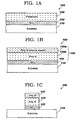
- FIG. 1A illustrates a cross-sectional view of the semiconductor structure 100 after a gate dielectric layer 120 and then a gate polysilicon layer 130 are formed on top of a semiconductor (e.g., silicon Si, germanium Ge, a mixture of Si and Ge, etc.) substrate 110, in accordance with embodiments of the present invention. More specifically, the fabrication process of the structure 100 of FIG. 1A starts out with the Si substrate 110. Then, in one embodiment, the gate dielectric layer 120 can be formed by thermally oxidizing a top surface of the Si substrate 110 in a first thermal oxidation step. As a result, the resulting gate dielectric layer 120 comprises silicon dioxide (SiO 2 ). Then, the gate polysilicon layer 130 can be formed by depositing silicon on top of the SiO 2 gate dielectric layer 120 using, illustratively, a CVD (chemical vapor deposition) process.
- a CVD chemical vapor deposition
- FIG. 1B illustrates a cross-sectional view of the semiconductor structure 100 after a heavily-doped gate polysilicon layer 130a is formed at top of the semiconductor structure 100 of FIG. 1A , in accordance with embodiments of the present invention. More specifically, in one embodiment, dopants of one type (e.g., n-type phosphorous or p-type boron) are implanted by ion implantation into a top layer 130a of the gate polysilicon layer 130. As a result, the gate polysilicon layer 130 comprises two layers: the heavily-doped gate polysilicon layer 130a and the undoped (or lightly doped) gate polysilicon layer 130b.
- dopants of one type e.g., n-type phosphorous or p-type boron
- FIG. 1C illustrates a cross-sectional view of the semiconductor structure 100 after portions of the gate polysilicon layer 130 and the gate dielectric layer 120 are removed so as to form a gate stack 132,134,122, in accordance with the present invention.
- a photoresist mask (not shown) is laid on a top surface 135 of the heavily-doped gate polysilicon layer 130a of FIG. 1B .
- the photoresist mask covers an area of the top surface 135 under which the gate stack 132,134,122 is to be formed.
- portions of the gate polysilicon layer 130 not covered by the photoresist mask is chemically etched away in a first chemical etching step.
- portions of the gate dielectric layer 120 not covered by the photoresist mask is chemically etched away a second chemical etching step.
- the gate stack 132,134,122 What remains of the gate polysilicon layer 130 and the gate dielectric layer 120 after the first and second chemical etching steps is the gate stack 132,134,122. More specifically, what remains of the heavily-doped gate polysilicon layer 130a after the first chemical etching step is the heavily-doped gate polysilicon region 132. What remains of the undoped gate polysilicon layer 130b after the first chemical etching step is the undoped gate polysilicon region 134. Finally, what remains of the gate dielectric layer 120 after the second chemical etching step is the gate dielectric region 122.
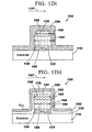
- FIG. 1Di illustrates a cross-sectional view of the semiconductor structure 100 after a spacer oxide layer 150 are formed on exposed surfaces of the gate stack 132,134,122 and the substrate 110 of FIG. 1C , in accordance with the present invention. More specifically, in one example, the semiconductor structure 100 of FIG. 1C is subjected to a second thermal oxidation step with the presence of oxygen (and/or oxygen-carrying material). As a result, oxygen reacts with silicon to form silicon dioxide SiO 2 constituting the spacer oxide layer 150. Assume that the gate polysilicon region 132 is doped with n-type dopants.
- the spacer oxide layer 150 is thicker at the heavily-doped gate polysilicon region 132 than at the undoped gate polysilicon region 134, meaning the thickness 162 is larger than the thickness 164 ( FIG. 1Di ).
- the width 166 (i.e., in direction 137) of the heavily-doped gate polysilicon region 132 is narrower than the width 168 of the undoped gate polysilicon region 134.
- FIG. 1Dii illustrates an embodiment of the structure 100 of FIG. 1Dii.
- FIG. 1Dii illustrates a cross-sectional view of the semiconductor structure 100 after a diffusion barrier layer 170 and a spacer oxide layer 180 are formed on exposed surfaces of the gate stack 132,134,122 and the substrate 110 of FIG. 1C , in accordance with the present invention. More specifically, in one embodiment, the semiconductor structure 100 of FIG. 1C is subjected to a third thermal oxidation step with the presence of oxygen (and/or oxygen-carrying material) and a nitrogen-carrying gas (e.g., N 2 O or NO).
- oxygen and/or oxygen-carrying material
- a nitrogen-carrying gas e.g., N 2 O or NO
- first, second, and third thermal oxidation steps refer to three separate, independent thermal oxidation steps and do not necessarily mean that all of the first, second, and third thermal oxidation steps must be performed in one embodiment, or that they must be performed in the order of first, second, and then third.
- the structure 100 of FIG. 1Dii involves only the first and third thermal oxidation steps (not the second thermal oxidation step).
- the third oxidation step with the presence of the nitrogen-carrying gas is performed in a furnace (not shown) at a high temperature, illustratively, in the range of 900°C -1100°C.
- the diffusion barrier layer 170 As a result of the third thermal oxidation step, nitrogen atoms diffuse into the gate polysilicon regions 132 and 134 of the gate stack 132,134,122 and reacts with silicon to form oxynitride silicon constituting the diffusion barrier layer 170 at a depth 185.
- the formation of the diffusion barrier layer 170 is self-limiting, meaning that the just-formed diffusion barrier layer 170 prevents more nitrogen atoms from diffusing through the diffusion barrier layer 170 itself.
- the diffusion barrier layer 170 also prevents more oxygen atoms (which, in one embodiment, can come from oxygen gas and/used for the third thermal oxidation step) from diffusing through it.
- the nitrogen-carrying gas can be replaced by any equivalent gas that can react with silicon to form a diffusion barrier layer capable of preventing oxygen and/or oxygen-carrying materials from diffusing through it.
- the diffusion barrier layer 170 and the spacer oxide layer 180 are simultaneously formed in the third thermal oxidation step.
- the diffusion barrier layer 170 can be formed first, and then the spacer oxide layer 180 is formed.
- the diffusion barrier layer 170 can be formed by implanting nitrogen in a top layer (not shown) under the exposed surfaces of the regions 132 and 134, and then raising the temperature at the exposed surfaces of the regions 132 and 134 so as to cause the implanted nitrogen to react with silicon of the regions 132 and 134 to form silicon nitride (Si 3 N 4 ) constituting the diffusion barrier layer 170.
- the spacer oxide layer 180 can be formed by depositing SiO 2 on top of the diffusion barrier layer 170 using, illustratively, a CVD step. It should be noted that like oxynitride silicon, silicon nitride also prevents oxygen diffusion.
- the oxynitride silicon diffusion barrier layer 170 is formed at the same depth 185 from the exposed surfaces of the gate polysilicon regions 132 and 134. As a result, the thickness 182 of the spacer oxide layer 180 resulting from the oxidation of the n-type doped polysilicon region 132 and the thickness 184 of the spacer oxide layer 180 resulting from the oxidation of the undoped polysilicon region 134 are equal. Because the diffusion barrier layer 170 has the same thickness whether it results from the nitridation of polysilicon of the region 132 or region 134, the widths 186 and 188 (in direction 197) of the polysilicon regions 132 and 134, respectively, are also equal.
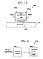
- FIG. 1E illustrates a cross-sectional view of the semiconductor structure 100 after top portions of the diffusion barrier layer 170 and the spacer oxide layer 180 above the gate stack 132,134,122 of FIG. 1Dii are removed, in accordance with embodiments of the present invention. More specifically, in one embodiment, the top portions of the diffusion barrier layer 170 and the spacer oxide layer 180 above the gate stack 132,134,122 ( FIG. 1Dii ) can be removed by, illustratively, a CMP (chemical mechanical polishing) step. What remains of the diffusion barrier layer 170 is the diffusion barrier regions 170a and 170b, and what remains of the spacer oxide layer 180 is the spacer oxide regions 180a and 180b. The spacer oxide regions 180a and 180b can be used to define source/drain regions (not shown) in the substrate 110.
- CMP chemical mechanical polishing
- FIG. 2 illustrates an oxidation system 200 for performing the third oxidation step described supra with respect to FIG. 1Dii .
- the oxidation system 200 comprises a pre-heat chamber 210 and an oxidation furnace 220 containing the structure 100 of FIG. 1C .
- the nitrogen-carrying gas is first heated up in the pre-heat chamber 210 to a high temperature (700 °C-900°C). Then, the pre-heated nitrogen-carrying gas is led to the oxidation furnace 220. In the oxidation furnace 220, the top surfaces of the structure 100 is also heated to 700 °C -900°C. At this temperature range, the third oxidation step occurs as described supra.
- the third oxidation step can be carried out in the oxidation furnace 220 at a lower temperature than without the preheating step (i.e., at 700 °C-900°C as opposed to 900°C-1100°C).
- the thin diffusion barrier layer 170 is formed at a same depth 185 in the gate polysilicon regions 132 and 134 regardless of doping concentration. Therefore, the resulting gate polysilicon regions 132 and 134 have equal widths 186 and 188, respectively ( FIG. 1Dii ). As a result, the region 132 of FIG. 1Dii is less likely to break off than the case of FIG. 1Di during ensuing fabrication steps (e.g., a chemical mechanical polishing step).
- the gate polysilicon region 134 is undoped.
- the gate polysilicon region 134 can be lightly doped with either n-type or p-type dopants or both.
Landscapes
- Engineering & Computer Science (AREA)
- Physics & Mathematics (AREA)
- Condensed Matter Physics & Semiconductors (AREA)
- General Physics & Mathematics (AREA)
- Manufacturing & Machinery (AREA)
- Computer Hardware Design (AREA)
- Microelectronics & Electronic Packaging (AREA)
- Power Engineering (AREA)
- Insulated Gate Type Field-Effect Transistor (AREA)
- Electrodes Of Semiconductors (AREA)
Applications Claiming Priority (2)
| Application Number | Priority Date | Filing Date | Title |
|---|---|---|---|
| US10/711,742 US7157341B2 (en) | 2004-10-01 | 2004-10-01 | Gate stacks |
| PCT/US2005/035455 WO2006039632A2 (en) | 2004-10-01 | 2005-09-30 | Gate stacks |
Publications (3)
| Publication Number | Publication Date |
|---|---|
| EP1805798A2 EP1805798A2 (en) | 2007-07-11 |
| EP1805798A4 EP1805798A4 (en) | 2009-08-05 |
| EP1805798B1 true EP1805798B1 (en) | 2014-08-13 |
Family
ID=36126115
Family Applications (1)
| Application Number | Title | Priority Date | Filing Date |
|---|---|---|---|
| EP05812439.7A Expired - Lifetime EP1805798B1 (en) | 2004-10-01 | 2005-09-30 | Method of forming a semiconductor structure |
Country Status (6)
| Country | Link |
|---|---|
| US (2) | US7157341B2 (enExample) |
| EP (1) | EP1805798B1 (enExample) |
| JP (1) | JP2008515240A (enExample) |
| CN (1) | CN101032024B (enExample) |
| TW (1) | TW200623270A (enExample) |
| WO (1) | WO2006039632A2 (enExample) |
Families Citing this family (9)
| Publication number | Priority date | Publication date | Assignee | Title |
|---|---|---|---|---|
| US8062707B2 (en) * | 2005-02-17 | 2011-11-22 | Konica Minolta Holdings, Inc. | Gas barrier film, gas barrier film manufacturing method, resin substrate for organic electroluminescent device using the aforesaid gas barrier film, and organic electroluminescent device using the aforementioned gas barrier film |
| US8486487B2 (en) | 2005-02-17 | 2013-07-16 | Konica Minolta Holdings, Inc. | Gas barrier film, gas barrier film manufacturing method, resin substrate for organic electroluminescent device using the aforesaid gas barrier film, and organic electroluminescent device using the aforementioned gas barrier film |
| US7271079B2 (en) * | 2005-04-06 | 2007-09-18 | International Business Machines Corporation | Method of doping a gate electrode of a field effect transistor |
| KR100633988B1 (ko) * | 2005-06-23 | 2006-10-13 | 동부일렉트로닉스 주식회사 | 반도체 소자 및 그 제조 방법 |
| JP2009026777A (ja) * | 2007-07-17 | 2009-02-05 | Renesas Technology Corp | 半導体装置の製造方法 |
| US8173532B2 (en) | 2007-07-30 | 2012-05-08 | International Business Machines Corporation | Semiconductor transistors having reduced distances between gate electrode regions |
| CN101728255B (zh) * | 2008-10-21 | 2011-07-20 | 中芯国际集成电路制造(北京)有限公司 | 在晶圆上制造栅极的方法 |
| JP2020035789A (ja) | 2018-08-27 | 2020-03-05 | キオクシア株式会社 | 半導体装置 |
| CN118055613A (zh) * | 2022-11-08 | 2024-05-17 | 长鑫存储技术有限公司 | 半导体结构及其形成方法 |
Family Cites Families (32)
| Publication number | Priority date | Publication date | Assignee | Title |
|---|---|---|---|---|
| JPS61190981A (ja) * | 1985-02-20 | 1986-08-25 | Casio Comput Co Ltd | 半導体装置 |
| JPH04142777A (ja) * | 1990-10-03 | 1992-05-15 | Kawasaki Steel Corp | ゲート電極又は配線の形成方法 |
| JP3316027B2 (ja) * | 1993-03-16 | 2002-08-19 | 株式会社半導体エネルギー研究所 | 絶縁ゲート型電界効果半導体装置の作製方法 |
| JP2536413B2 (ja) * | 1993-06-28 | 1996-09-18 | 日本電気株式会社 | 半導体集積回路装置の製造方法 |
| US5459091A (en) * | 1993-10-12 | 1995-10-17 | Goldstar Electron Co., Ltd. | Method for fabricating a non-volatile memory device |
| FR2711275B1 (fr) * | 1993-10-15 | 1996-10-31 | Intel Corp | Procédé automatiquement aligné de contact en fabrication de semi-conducteurs et dispositifs produits. |
| US5545581A (en) * | 1994-12-06 | 1996-08-13 | International Business Machines Corporation | Plug strap process utilizing selective nitride and oxide etches |
| JP3390895B2 (ja) * | 1995-05-19 | 2003-03-31 | 富士通株式会社 | Mos型半導体装置の製造方法 |
| DE19526184A1 (de) * | 1995-07-18 | 1997-04-03 | Siemens Ag | Verfahren zur Herstellung eines MOS-Transistors |
| JP3145929B2 (ja) * | 1996-08-15 | 2001-03-12 | 日本電気株式会社 | 半導体装置の製造方法 |
| JPH1167927A (ja) * | 1997-06-09 | 1999-03-09 | Mitsubishi Electric Corp | 半導体装置およびその製造方法 |
| FR2765394B1 (fr) * | 1997-06-25 | 1999-09-24 | France Telecom | Procede d'obtention d'un transistor a grille en silicium-germanium |
| JPH11135773A (ja) * | 1997-10-27 | 1999-05-21 | Fujitsu Ltd | 半導体装置及びその製造方法 |
| US6278165B1 (en) * | 1998-06-29 | 2001-08-21 | Kabushiki Kaisha Toshiba | MIS transistor having a large driving current and method for producing the same |
| US6143611A (en) * | 1998-07-30 | 2000-11-07 | Micron Technology, Inc. | Semiconductor processing methods, methods of forming electronic components, and transistors |
| US6483736B2 (en) * | 1998-11-16 | 2002-11-19 | Matrix Semiconductor, Inc. | Vertically stacked field programmable nonvolatile memory and method of fabrication |
| JP2000269490A (ja) * | 1999-03-16 | 2000-09-29 | Fujitsu Ltd | 半導体装置の製造方法 |
| US6265297B1 (en) * | 1999-09-01 | 2001-07-24 | Micron Technology, Inc. | Ammonia passivation of metal gate electrodes to inhibit oxidation of metal |
| JP2001326348A (ja) * | 2000-05-16 | 2001-11-22 | Mitsubishi Electric Corp | 半導体装置の製造方法及び半導体装置 |
| US6624011B1 (en) * | 2000-08-14 | 2003-09-23 | Matrix Semiconductor, Inc. | Thermal processing for three dimensional circuits |
| US6562684B1 (en) * | 2000-08-30 | 2003-05-13 | Micron Technology, Inc. | Methods of forming dielectric materials |
| US20020072210A1 (en) * | 2000-11-29 | 2002-06-13 | Chi-Min Hsu | Method for forming liner layer in sin spacer |
| JP4932087B2 (ja) * | 2001-01-29 | 2012-05-16 | 三菱電機株式会社 | 半導体装置およびその製造方法 |
| US6525953B1 (en) * | 2001-08-13 | 2003-02-25 | Matrix Semiconductor, Inc. | Vertically-stacked, field-programmable, nonvolatile memory and method of fabrication |
| US6812515B2 (en) * | 2001-11-26 | 2004-11-02 | Hynix Semiconductor, Inc. | Polysilicon layers structure and method of forming same |
| JP3873771B2 (ja) * | 2002-02-22 | 2007-01-24 | ソニー株式会社 | 半導体装置の製造方法 |
| US7098098B2 (en) | 2002-04-16 | 2006-08-29 | Texas Instruments Incorporated | Methods for transistors formation using selective gate implantation |
| JP3487844B1 (ja) * | 2002-06-14 | 2004-01-19 | 沖電気工業株式会社 | Ldmos型半導体装置の製造方法 |
| US20040033677A1 (en) * | 2002-08-14 | 2004-02-19 | Reza Arghavani | Method and apparatus to prevent lateral oxidation in a transistor utilizing an ultra thin oxygen-diffusion barrier |
| US6686637B1 (en) * | 2002-11-21 | 2004-02-03 | International Business Machines Corporation | Gate structure with independently tailored vertical doping profile |
| US20050048732A1 (en) * | 2003-08-26 | 2005-03-03 | International Business Machines Corporation | Method to produce transistor having reduced gate height |
| US6930362B1 (en) * | 2003-10-30 | 2005-08-16 | Lsi Logic Corporation | Calcium doped polysilicon gate electrodes |
-
2004
- 2004-10-01 US US10/711,742 patent/US7157341B2/en not_active Expired - Fee Related
-
2005
- 2005-09-30 EP EP05812439.7A patent/EP1805798B1/en not_active Expired - Lifetime
- 2005-09-30 JP JP2007534850A patent/JP2008515240A/ja active Pending
- 2005-09-30 CN CN2005800333850A patent/CN101032024B/zh not_active Expired - Fee Related
- 2005-09-30 WO PCT/US2005/035455 patent/WO2006039632A2/en not_active Ceased
- 2005-09-30 TW TW094134172A patent/TW200623270A/zh unknown
-
2006
- 2006-08-08 US US11/463,039 patent/US7378712B2/en not_active Expired - Fee Related
Also Published As
| Publication number | Publication date |
|---|---|
| TW200623270A (en) | 2006-07-01 |
| EP1805798A2 (en) | 2007-07-11 |
| CN101032024B (zh) | 2011-02-09 |
| JP2008515240A (ja) | 2008-05-08 |
| WO2006039632A3 (en) | 2006-08-10 |
| WO2006039632A2 (en) | 2006-04-13 |
| EP1805798A4 (en) | 2009-08-05 |
| CN101032024A (zh) | 2007-09-05 |
| US20070194385A1 (en) | 2007-08-23 |
| US20060073688A1 (en) | 2006-04-06 |
| US7378712B2 (en) | 2008-05-27 |
| US7157341B2 (en) | 2007-01-02 |
Similar Documents
| Publication | Publication Date | Title |
|---|---|---|
| US6475888B1 (en) | Method for forming ultra-shallow junctions using laser annealing | |
| US6160299A (en) | Shallow-implant elevated source/drain doping from a sidewall dopant source | |
| US7462528B2 (en) | CMOS (Complementary metal oxide semiconductor) technology with leakage current mitigation | |
| US6812073B2 (en) | Source drain and extension dopant concentration | |
| JP2877104B2 (ja) | 半導体装置の製造方法 | |
| US6677201B1 (en) | Method of fabricating thermal CVD oxynitride and BTBAS nitride sidewall spacer for metal oxide semiconductor transistors | |
| EP1805798B1 (en) | Method of forming a semiconductor structure | |
| US6620668B2 (en) | Method of fabricating MOS transistor having shallow source/drain junction regions | |
| KR100426482B1 (ko) | 플래쉬 메모리 셀의 제조 방법 | |
| US6362062B1 (en) | Disposable sidewall spacer process for integrated circuits | |
| US20020168828A1 (en) | Method of reducing threshold voltage shifting of a gate | |
| KR100632168B1 (ko) | 반도체 장치 및 그 제조방법 | |
| US20080044991A1 (en) | Semiconductor device and method of fabricating the same | |
| US20090286375A1 (en) | Method of forming sidewall spacers to reduce formation of recesses in the substrate and increase dopant retention in a semiconductor device | |
| US6541322B2 (en) | Method for preventing gate depletion effects of MOS transistor | |
| KR940011478B1 (ko) | 반도체 장치의 제조방법 | |
| US7365362B2 (en) | Semiconductor device and method of fabricating semiconductor device using oxidation | |
| JP4719422B2 (ja) | 半導体装置の製造方法 | |
| US20030143813A1 (en) | Semiconductor device and method | |
| KR100451768B1 (ko) | 반도체 소자의 게이트 절연막 형성 방법 | |
| KR100306812B1 (ko) | 반도체 소자의 게이트 형성방법 | |
| KR100904729B1 (ko) | 반도체소자의 듀얼 게이트 형성방법 | |
| KR20000050488A (ko) | 듀얼 게이트 구조를 갖는 반도체 장치의 제조 방법 | |
| KR20040054053A (ko) | 반도체 소자 제조 방법 | |
| JP2004342722A (ja) | 半導体装置および半導体装置の製造方法 |
Legal Events
| Date | Code | Title | Description |
|---|---|---|---|
| PUAI | Public reference made under article 153(3) epc to a published international application that has entered the european phase |
Free format text: ORIGINAL CODE: 0009012 |
|
| 17P | Request for examination filed |
Effective date: 20070427 |
|
| AK | Designated contracting states |
Kind code of ref document: A2 Designated state(s): AT BE BG CH CY CZ DE DK EE ES FI FR GB GR HU IE IS IT LI LT LU LV MC NL PL PT RO SE SI SK TR |
|
| DAX | Request for extension of the european patent (deleted) | ||
| A4 | Supplementary search report drawn up and despatched |
Effective date: 20090707 |
|
| 17Q | First examination report despatched |
Effective date: 20110218 |
|
| REG | Reference to a national code |
Ref country code: DE Ref legal event code: R079 Ref document number: 602005044495 Country of ref document: DE Free format text: PREVIOUS MAIN CLASS: H01L0023480000 Ipc: H01L0021280000 |
|
| RIC1 | Information provided on ipc code assigned before grant |
Ipc: H01L 23/48 20060101ALI20140211BHEP Ipc: H01L 21/336 20060101ALI20140211BHEP Ipc: H01L 21/302 20060101ALI20140211BHEP Ipc: H01L 21/4763 20060101ALI20140211BHEP Ipc: H01L 21/469 20060101ALI20140211BHEP Ipc: H01L 21/28 20060101AFI20140211BHEP Ipc: H01L 29/49 20060101ALI20140211BHEP |
|
| GRAP | Despatch of communication of intention to grant a patent |
Free format text: ORIGINAL CODE: EPIDOSNIGR1 |
|
| INTG | Intention to grant announced |
Effective date: 20140415 |
|
| GRAS | Grant fee paid |
Free format text: ORIGINAL CODE: EPIDOSNIGR3 |
|
| GRAA | (expected) grant |
Free format text: ORIGINAL CODE: 0009210 |
|
| AK | Designated contracting states |
Kind code of ref document: B1 Designated state(s): AT BE BG CH CY CZ DE DK EE ES FI FR GB GR HU IE IS IT LI LT LU LV MC NL PL PT RO SE SI SK TR |
|
| REG | Reference to a national code |
Ref country code: GB Ref legal event code: FG4D |
|
| REG | Reference to a national code |
Ref country code: AT Ref legal event code: REF Ref document number: 682656 Country of ref document: AT Kind code of ref document: T Effective date: 20140815 Ref country code: CH Ref legal event code: EP |
|
| REG | Reference to a national code |
Ref country code: DE Ref legal event code: R081 Ref document number: 602005044495 Country of ref document: DE Owner name: GLOBALFOUNDRIES INC., KY Free format text: FORMER OWNER: INTERNATIONAL BUSINESS MACHINES CORPORATION, ARMONK, N.Y., US |
|
| REG | Reference to a national code |
Ref country code: CH Ref legal event code: NV Representative=s name: IBM RESEARCH GMBH ZURICH RESEARCH LABORATORY I, CH |
|
| REG | Reference to a national code |
Ref country code: DE Ref legal event code: R084 Ref document number: 602005044495 Country of ref document: DE |
|
| REG | Reference to a national code |
Ref country code: IE Ref legal event code: FG4D |
|
| REG | Reference to a national code |
Ref country code: DE Ref legal event code: R096 Ref document number: 602005044495 Country of ref document: DE Effective date: 20140925 |
|
| REG | Reference to a national code |
Ref country code: GB Ref legal event code: 746 Effective date: 20140909 |
|
| REG | Reference to a national code |
Ref country code: DE Ref legal event code: R084 Ref document number: 602005044495 Country of ref document: DE Effective date: 20140904 |
|
| REG | Reference to a national code |
Ref country code: NL Ref legal event code: VDEP Effective date: 20140813 |
|
| REG | Reference to a national code |
Ref country code: AT Ref legal event code: MK05 Ref document number: 682656 Country of ref document: AT Kind code of ref document: T Effective date: 20140813 |
|
| REG | Reference to a national code |
Ref country code: LT Ref legal event code: MG4D |
|
| PG25 | Lapsed in a contracting state [announced via postgrant information from national office to epo] |
Ref country code: PT Free format text: LAPSE BECAUSE OF FAILURE TO SUBMIT A TRANSLATION OF THE DESCRIPTION OR TO PAY THE FEE WITHIN THE PRESCRIBED TIME-LIMIT Effective date: 20141215 Ref country code: FI Free format text: LAPSE BECAUSE OF FAILURE TO SUBMIT A TRANSLATION OF THE DESCRIPTION OR TO PAY THE FEE WITHIN THE PRESCRIBED TIME-LIMIT Effective date: 20140813 Ref country code: BG Free format text: LAPSE BECAUSE OF FAILURE TO SUBMIT A TRANSLATION OF THE DESCRIPTION OR TO PAY THE FEE WITHIN THE PRESCRIBED TIME-LIMIT Effective date: 20141113 Ref country code: ES Free format text: LAPSE BECAUSE OF FAILURE TO SUBMIT A TRANSLATION OF THE DESCRIPTION OR TO PAY THE FEE WITHIN THE PRESCRIBED TIME-LIMIT Effective date: 20140813 Ref country code: SE Free format text: LAPSE BECAUSE OF FAILURE TO SUBMIT A TRANSLATION OF THE DESCRIPTION OR TO PAY THE FEE WITHIN THE PRESCRIBED TIME-LIMIT Effective date: 20140813 Ref country code: GR Free format text: LAPSE BECAUSE OF FAILURE TO SUBMIT A TRANSLATION OF THE DESCRIPTION OR TO PAY THE FEE WITHIN THE PRESCRIBED TIME-LIMIT Effective date: 20141114 Ref country code: LT Free format text: LAPSE BECAUSE OF FAILURE TO SUBMIT A TRANSLATION OF THE DESCRIPTION OR TO PAY THE FEE WITHIN THE PRESCRIBED TIME-LIMIT Effective date: 20140813 |
|
| PG25 | Lapsed in a contracting state [announced via postgrant information from national office to epo] |
Ref country code: IS Free format text: LAPSE BECAUSE OF FAILURE TO SUBMIT A TRANSLATION OF THE DESCRIPTION OR TO PAY THE FEE WITHIN THE PRESCRIBED TIME-LIMIT Effective date: 20141213 Ref country code: AT Free format text: LAPSE BECAUSE OF FAILURE TO SUBMIT A TRANSLATION OF THE DESCRIPTION OR TO PAY THE FEE WITHIN THE PRESCRIBED TIME-LIMIT Effective date: 20140813 Ref country code: CY Free format text: LAPSE BECAUSE OF FAILURE TO SUBMIT A TRANSLATION OF THE DESCRIPTION OR TO PAY THE FEE WITHIN THE PRESCRIBED TIME-LIMIT Effective date: 20140813 Ref country code: LV Free format text: LAPSE BECAUSE OF FAILURE TO SUBMIT A TRANSLATION OF THE DESCRIPTION OR TO PAY THE FEE WITHIN THE PRESCRIBED TIME-LIMIT Effective date: 20140813 |
|
| PG25 | Lapsed in a contracting state [announced via postgrant information from national office to epo] |
Ref country code: NL Free format text: LAPSE BECAUSE OF FAILURE TO SUBMIT A TRANSLATION OF THE DESCRIPTION OR TO PAY THE FEE WITHIN THE PRESCRIBED TIME-LIMIT Effective date: 20140813 |
|
| PG25 | Lapsed in a contracting state [announced via postgrant information from national office to epo] |
Ref country code: IT Free format text: LAPSE BECAUSE OF FAILURE TO SUBMIT A TRANSLATION OF THE DESCRIPTION OR TO PAY THE FEE WITHIN THE PRESCRIBED TIME-LIMIT Effective date: 20140813 Ref country code: RO Free format text: LAPSE BECAUSE OF FAILURE TO SUBMIT A TRANSLATION OF THE DESCRIPTION OR TO PAY THE FEE WITHIN THE PRESCRIBED TIME-LIMIT Effective date: 20140813 Ref country code: CZ Free format text: LAPSE BECAUSE OF FAILURE TO SUBMIT A TRANSLATION OF THE DESCRIPTION OR TO PAY THE FEE WITHIN THE PRESCRIBED TIME-LIMIT Effective date: 20140813 Ref country code: DK Free format text: LAPSE BECAUSE OF FAILURE TO SUBMIT A TRANSLATION OF THE DESCRIPTION OR TO PAY THE FEE WITHIN THE PRESCRIBED TIME-LIMIT Effective date: 20140813 Ref country code: EE Free format text: LAPSE BECAUSE OF FAILURE TO SUBMIT A TRANSLATION OF THE DESCRIPTION OR TO PAY THE FEE WITHIN THE PRESCRIBED TIME-LIMIT Effective date: 20140813 Ref country code: SK Free format text: LAPSE BECAUSE OF FAILURE TO SUBMIT A TRANSLATION OF THE DESCRIPTION OR TO PAY THE FEE WITHIN THE PRESCRIBED TIME-LIMIT Effective date: 20140813 |
|
| REG | Reference to a national code |
Ref country code: CH Ref legal event code: PL |
|
| REG | Reference to a national code |
Ref country code: DE Ref legal event code: R097 Ref document number: 602005044495 Country of ref document: DE |
|
| PG25 | Lapsed in a contracting state [announced via postgrant information from national office to epo] |
Ref country code: PL Free format text: LAPSE BECAUSE OF FAILURE TO SUBMIT A TRANSLATION OF THE DESCRIPTION OR TO PAY THE FEE WITHIN THE PRESCRIBED TIME-LIMIT Effective date: 20140813 Ref country code: MC Free format text: LAPSE BECAUSE OF FAILURE TO SUBMIT A TRANSLATION OF THE DESCRIPTION OR TO PAY THE FEE WITHIN THE PRESCRIBED TIME-LIMIT Effective date: 20140813 |
|
| PLBE | No opposition filed within time limit |
Free format text: ORIGINAL CODE: 0009261 |
|
| STAA | Information on the status of an ep patent application or granted ep patent |
Free format text: STATUS: NO OPPOSITION FILED WITHIN TIME LIMIT |
|
| REG | Reference to a national code |
Ref country code: FR Ref legal event code: ST Effective date: 20150529 |
|
| PG25 | Lapsed in a contracting state [announced via postgrant information from national office to epo] |
Ref country code: BE Free format text: LAPSE BECAUSE OF NON-PAYMENT OF DUE FEES Effective date: 20140930 |
|
| REG | Reference to a national code |
Ref country code: IE Ref legal event code: MM4A |
|
| 26N | No opposition filed |
Effective date: 20150515 |
|
| PG25 | Lapsed in a contracting state [announced via postgrant information from national office to epo] |
Ref country code: LI Free format text: LAPSE BECAUSE OF NON-PAYMENT OF DUE FEES Effective date: 20140930 Ref country code: CH Free format text: LAPSE BECAUSE OF NON-PAYMENT OF DUE FEES Effective date: 20140930 |
|
| PG25 | Lapsed in a contracting state [announced via postgrant information from national office to epo] |
Ref country code: IE Free format text: LAPSE BECAUSE OF NON-PAYMENT OF DUE FEES Effective date: 20140930 Ref country code: FR Free format text: LAPSE BECAUSE OF NON-PAYMENT OF DUE FEES Effective date: 20141013 |
|
| PGFP | Annual fee paid to national office [announced via postgrant information from national office to epo] |
Ref country code: GB Payment date: 20150930 Year of fee payment: 11 |
|
| PG25 | Lapsed in a contracting state [announced via postgrant information from national office to epo] |
Ref country code: SI Free format text: LAPSE BECAUSE OF FAILURE TO SUBMIT A TRANSLATION OF THE DESCRIPTION OR TO PAY THE FEE WITHIN THE PRESCRIBED TIME-LIMIT Effective date: 20140813 |
|
| REG | Reference to a national code |
Ref country code: DE Ref legal event code: R082 Ref document number: 602005044495 Country of ref document: DE Representative=s name: RICHARDT PATENTANWAELTE PARTG MBB, DE Ref country code: DE Ref legal event code: R081 Ref document number: 602005044495 Country of ref document: DE Owner name: GLOBALFOUNDRIES INC., KY Free format text: FORMER OWNER: INTERNATIONAL BUSINESS MACHINES CORP., ARMONK, N.Y., US |
|
| REG | Reference to a national code |
Ref country code: DE Ref legal event code: R082 Ref document number: 602005044495 Country of ref document: DE Representative=s name: RICHARDT PATENTANWAELTE PARTG MBB, DE Ref country code: DE Ref legal event code: R081 Ref document number: 602005044495 Country of ref document: DE Owner name: GLOBALFOUNDRIES INC., KY Free format text: FORMER OWNER: GLOBALFOUNDRIES US 2 LLC (N.D.GES.DES STAATES DELAWARE), HOPEWELL JUNCTION, N.Y., US |
|
| PG25 | Lapsed in a contracting state [announced via postgrant information from national office to epo] |
Ref country code: TR Free format text: LAPSE BECAUSE OF FAILURE TO SUBMIT A TRANSLATION OF THE DESCRIPTION OR TO PAY THE FEE WITHIN THE PRESCRIBED TIME-LIMIT Effective date: 20140813 Ref country code: BE Free format text: LAPSE BECAUSE OF FAILURE TO SUBMIT A TRANSLATION OF THE DESCRIPTION OR TO PAY THE FEE WITHIN THE PRESCRIBED TIME-LIMIT Effective date: 20140813 Ref country code: LU Free format text: LAPSE BECAUSE OF NON-PAYMENT OF DUE FEES Effective date: 20140930 Ref country code: HU Free format text: LAPSE BECAUSE OF FAILURE TO SUBMIT A TRANSLATION OF THE DESCRIPTION OR TO PAY THE FEE WITHIN THE PRESCRIBED TIME-LIMIT; INVALID AB INITIO Effective date: 20050930 |
|
| GBPC | Gb: european patent ceased through non-payment of renewal fee |
Effective date: 20160930 |
|
| PG25 | Lapsed in a contracting state [announced via postgrant information from national office to epo] |
Ref country code: GB Free format text: LAPSE BECAUSE OF NON-PAYMENT OF DUE FEES Effective date: 20160930 |
|
| PGFP | Annual fee paid to national office [announced via postgrant information from national office to epo] |
Ref country code: DE Payment date: 20170927 Year of fee payment: 13 |
|
| REG | Reference to a national code |
Ref country code: DE Ref legal event code: R119 Ref document number: 602005044495 Country of ref document: DE |
|
| PG25 | Lapsed in a contracting state [announced via postgrant information from national office to epo] |
Ref country code: DE Free format text: LAPSE BECAUSE OF NON-PAYMENT OF DUE FEES Effective date: 20190402 |