EP1777941B1 - Wide-angle imaging lens system - Google Patents
Wide-angle imaging lens system Download PDFInfo
- Publication number
- EP1777941B1 EP1777941B1 EP06022048A EP06022048A EP1777941B1 EP 1777941 B1 EP1777941 B1 EP 1777941B1 EP 06022048 A EP06022048 A EP 06022048A EP 06022048 A EP06022048 A EP 06022048A EP 1777941 B1 EP1777941 B1 EP 1777941B1
- Authority
- EP
- European Patent Office
- Prior art keywords
- lens
- wide
- angle imaging
- image
- imaging lens
- Prior art date
- Legal status (The legal status is an assumption and is not a legal conclusion. Google has not performed a legal analysis and makes no representation as to the accuracy of the status listed.)
- Not-in-force
Links
- 238000003384 imaging method Methods 0.000 title claims abstract description 181
- 230000003287 optical effect Effects 0.000 claims description 55
- 239000000463 material Substances 0.000 claims description 24
- 238000010521 absorption reaction Methods 0.000 claims description 10
- XLYOFNOQVPJJNP-UHFFFAOYSA-N water Substances O XLYOFNOQVPJJNP-UHFFFAOYSA-N 0.000 claims description 10
- 230000008859 change Effects 0.000 claims description 9
- 230000007423 decrease Effects 0.000 claims description 9
- 230000002093 peripheral effect Effects 0.000 claims description 9
- 229920003023 plastic Polymers 0.000 claims description 6
- 239000004033 plastic Substances 0.000 claims description 6
- 230000005499 meniscus Effects 0.000 claims description 4
- 230000004075 alteration Effects 0.000 description 59
- 238000010586 diagram Methods 0.000 description 17
- 201000009310 astigmatism Diseases 0.000 description 14
- 230000015556 catabolic process Effects 0.000 description 4
- 239000006059 cover glass Substances 0.000 description 4
- 238000006731 degradation reaction Methods 0.000 description 4
- 239000011521 glass Substances 0.000 description 4
- 230000004048 modification Effects 0.000 description 2
- 238000012986 modification Methods 0.000 description 2
- 238000000465 moulding Methods 0.000 description 2
- 230000015572 biosynthetic process Effects 0.000 description 1
- 230000000295 complement effect Effects 0.000 description 1
- 229910044991 metal oxide Inorganic materials 0.000 description 1
- 150000004706 metal oxides Chemical class 0.000 description 1
- 239000003973 paint Substances 0.000 description 1
- 239000004065 semiconductor Substances 0.000 description 1
- 239000013585 weight reducing agent Substances 0.000 description 1
- 230000003245 working effect Effects 0.000 description 1
Images


Classifications
-
- G—PHYSICS
- G02—OPTICS
- G02B—OPTICAL ELEMENTS, SYSTEMS OR APPARATUS
- G02B13/00—Optical objectives specially designed for the purposes specified below
- G02B13/001—Miniaturised objectives for electronic devices, e.g. portable telephones, webcams, PDAs, small digital cameras
- G02B13/0015—Miniaturised objectives for electronic devices, e.g. portable telephones, webcams, PDAs, small digital cameras characterised by the lens design
- G02B13/002—Miniaturised objectives for electronic devices, e.g. portable telephones, webcams, PDAs, small digital cameras characterised by the lens design having at least one aspherical surface
- G02B13/0035—Miniaturised objectives for electronic devices, e.g. portable telephones, webcams, PDAs, small digital cameras characterised by the lens design having at least one aspherical surface having three lenses
-
- G—PHYSICS
- G02—OPTICS
- G02B—OPTICAL ELEMENTS, SYSTEMS OR APPARATUS
- G02B13/00—Optical objectives specially designed for the purposes specified below
- G02B13/04—Reversed telephoto objectives
-
- G—PHYSICS
- G02—OPTICS
- G02B—OPTICAL ELEMENTS, SYSTEMS OR APPARATUS
- G02B13/00—Optical objectives specially designed for the purposes specified below
- G02B13/18—Optical objectives specially designed for the purposes specified below with lenses having one or more non-spherical faces, e.g. for reducing geometrical aberration
-
- G—PHYSICS
- G02—OPTICS
- G02B—OPTICAL ELEMENTS, SYSTEMS OR APPARATUS
- G02B9/00—Optical objectives characterised both by the number of the components and their arrangements according to their sign, i.e. + or -
- G02B9/12—Optical objectives characterised both by the number of the components and their arrangements according to their sign, i.e. + or - having three components only
Definitions
- the present invention relates to an imaging lens that is used in a vehicular camera, a cell phone camera, a surveillance camera, or the like having an imaging device such as a CCD (charge-coupled device) sensor or a CMOS (complementary metal oxide semiconductor) sensor. And the invention mainly relates to, for example, a wide-angle imaging lens that is used in a vehicular camera for taking an image of a front sight, a side sight, a rear sight, or the like as viewed from a vehicle.
- an imaging device such as a CCD (charge-coupled device) sensor or a CMOS (complementary metal oxide semiconductor) sensor.
- the invention mainly relates to, for example, a wide-angle imaging lens that is used in a vehicular camera for taking an image of a front sight, a side sight, a rear sight, or the like as viewed from a vehicle.
- imaging devices such as CCD sensors and CMOS sensors have been increased greatly in miniaturization and the number of pixels. Accordingly, imaging apparatus main bodies and lenses mounted thereon are required to be reduced in size and weight. On the other hand, a wide-angle lens having a large angle of view (e.g., 140° or more diagonally) is required in vehicular cameras etc.
- JP-A-7-72382 JP-A-2001-337268 JP-A-2005-181596 and JP-A-2002-244031 .
- JP-A-7-72382 and JP-A-2005-181596 disclose wide-angle lenses for CCD cameras which have a three-lens configuration.
- JP-A-2001-337268 discloses a wide-angle lens including three aspherical lenses.
- JP-A-2002-244031 discloses a wide-angle lens including a total of four lenses which are divided into a first group and a second group.
- the wide-angle lens of JP-A-7-72382 is not sufficient in miniaturization and angle-of-view increase.
- the wide-angle lens of JP-A-2001-337268 employs a plastic aspherical lens as the first lens.
- the first lens be made of glass.
- since the first lens is an aspherical lens, forming the first lens with glass is costly.
- the wide-angle lens of JP-A-2002-244031 which consists of four lenses, is disadvantageous in cost and weight reduction though it is advantageous in performance.
- An object of the invention is to provide a wide-angle imaging lens, which can be realized at a low cost as a compact, lightweight wide-angle lens system which exhibits good optical performance.
- a wide-angle imaging lens includes: in order from an object side of the wide-angle imaging lens, a first lens of a negative meniscus lens having a convex surface on the object side thereof; a second lens, at least one surface of which is an aspherical surface; and a positive third lens having a convex surface on an image side thereof, at least one surface of the third lens being an aspherical surface.
- the first lens is made of a material having an Abbe number of 40 or more and the third lens is made of a material having an Abbe number of 50 or more.
- An aperture stop is disposed between the second lens and the third lens.
- the object-side surface of the second lens is shaped in such a manner as to be a concave surface on an optical axis of the second lens and to decrease in negative power of the object-side surface as a position on the object-side surface goes away from the optical axis.
- the wide-angle imaging lens can be realized at a low cost as a compact, lightweight wide-angle lens system which exhibits good optical performance because the aspherical surface shapes, the lens materials, etc. are optimized by using a small number of (i.e., three) lenses.
- both surfaces of each of the second lens and the third lens be aspherical surfaces.
- each of the second lens and the third lens be made of plastics. It is preferable that each of the second lens and the third lens be made of a material whose coefficient of water absorption is 0.3% or less. Furthermore, it is preferable that the third lens be made of a polyolefin-type material.
- the object-side surface of the second lens may be shaped in such a manner as to change from the concave surface to a convex surface in a peripheral portion of the object-side surface as the position goes away from the optical axis.
- the image-side surface of the second lens be shaped in such a manner as to be a concave surface on the optical axis and to increase in negative power of the image-side surface as a position on the image-side surface goes away from the optical axis.
- the image-side surface of the second lens be shaped in such a manner as to be a convex surface on the optical axis and to decrease in positive power of the image-side surface as the position goes away from the optical axis.
- the image-side surface of the second lens may be shaped in such a manner as to change from the convex surface to a concave surface in a peripheral portion of the image-side surface as the position goes away from the optical axis.
- L is the distance between the top of the object-side surface of the first lens and the imaging device surface
- BF is the distance between the top of the image-side surface of the third lens and the imaging device surface.
- f is the focal length of the wide-angle imaging lens
- f1 is the focal length of the first lens
- L is the distance between the top of the object-side surface of the first lens and the imaging device surface
- x is the maximum image height
- 2 ⁇ is the diagonal angle of view in radian.
- a wide-angle imaging lens includes: in order from the object side, a first lens of a negative meniscus lens having a convex surface on the object side; a second lens, at least one surface of which is an aspherical surface; and a positive third lens having a convex surface on the image-side, at least one surface of the third lens being an aspherical surface.
- the aspherical surface shapes, the lens materials, etc. are optimized by using a small number of (i.e., three) lenses. As a result, as a compact, lightweight wide-angle lens system which exhibits good optical performance is realized at a low cost.
- Fig. 1 shows an exemplary configuration of a wide-angle imaging lens according to an exemplary embodiment of the invention. This exemplary configuration corresponds to the lens configuration of a first numerical value Example (described later).
- This wide-angle imaging lens is suitable for use in various cameras using an imaging device such as a CCD sensor or a CMOS sensor, for example, vehicular cameras for taking an image of a front sight, a side sight, a rear sight, or the like as viewed from a vehicle.
- This wide-angle imaging lens is equipped with a first lens L1, a second lens L2, and a third lens L3 which are arranged in this order from the object side along the optical axis Z1.
- An aperture stop St is disposed on the optical axis Z1 between the second lens L2 and the third lens L3.
- the diagonal angle of view is as wide as 140° or more.
- An imaging device 3 such as a CCD sensor is disposed in the image-forming plane of this wide-angle imaging lens.
- Various optical members 2 may be disposed between the third lens L3 and the imaging device 3 in accordance with the configuration of a camera to which the lens is attached.
- a plate-like optical member such as a cover glass for imaging surface protection or an infrared-blocking filter may be disposed there.
- a light beam that enters the lens system through outside the effective diameter range that is set between the first lens L1 and the second lens L2 may reach the image surface as stray light and produce a ghost.
- a light beam 4 is a light beam that enters the lens system at the maximum angle of the angle-of-view range. Light beams traveling outside the light beam 4 may become stray light. To avoid this phenomenon, it is preferable to interrupt stray light by disposing a light shield unit 1 between the first lens L1 and the second lens L2.
- the light shield unit 1 is an opaque plate member, for example. Alternatively, opaque paint may be applied to the portion, outside the effective diameter range, of the second-lens-L2-side surface of the first lens L1.
- the first lens L1 is a negative meniscus lens whose object-side surface is a convex surface. It is preferable that the first lens L1 be a spherical lens made of glass.
- the second lens L2 is a positive or negative lens which has relatively small power and at least one surface of which is an aspherical surface.
- the third lens L3 is a positive lens whose image-side surface is a convex surface (i.e., projected toward the image side) and at least one surface of which is an aspherical surface.
- the first lens L 1 is made of a material whose Abbe number is 40 or more and the third lens L3 is made of a material whose Abbe number is 50 or more.
- both surfaces of each of the second lens L2 and the third lens L3 be aspherical surfaces. It is preferable that the second lens L2 and the third lens L3 be made of plastics. It is preferable that the materials of the second lens L2 and the third lens L3 have coefficients of water absorption (weight%) that are 0.3% or less. More specifically, it is preferable that the third lens L3 be made of a polyolefin-type material. It is preferable that the second lens L2 also be made of a polyolefin-type material.
- the object-side surface of the second lens L2 is shaped in such a manner that it is concave (i.e., recessed) on the optical axis Z1 and its negative power decreases as the position goes away from the optical axis Z1.
- the object-side surface of the second lens L2 may be shaped in such a manner as to have a curvature inflection point in the effective diameter range and to change from a concave surface (i.e., recessed) to a convex surface (i.e., projected toward the object side) in the peripheral portion as the position goes away from the optical axis Z1.
- the image-side surface of the second lens L2 be shaped in such a manner that it is concave (i.e., recessed) near the optical axis Z1 and its negative power increases as the position goes away from the optical axis Z1.
- the image-side surface of the second lens L2 may be shaped in such a manner that it is convex (i.e., projected toward the image side) near the optical axis Z1 and its positive power decreases as the position goes away from the optical axis Z1.
- the image-side surface of the second lens L2 may be shaped in such a manner as to have a curvature inflection point in the effective diameter range and to change from a convex surface (i.e., projected toward the image side) to a concave surface (i.e., recessed) in the peripheral portion as the position goes away from the optical axis Z1.
- this wide-angle imaging lens satisfy: 3 ⁇ L / BF ⁇ 7 where L is the distance between the top of the object-side surface of the first lens L1 and the surface of the imaging device 3, and BF is the distance between the top of the image-side surface of the third lens L3 and the surface of the imaging device 3 (see Fig. 1 ).
- the distances L and BF are such that the thickness of the optical member 2 such as a cover glass is air-converted.
- this wide-angle imaging lens satisfy: 2 ⁇ f ⁇ 1 / f ⁇ 11 where f is the focal length of the entire lens system, and f1 is the focal length of the first lens L1.
- this wide-angle imaging lens satisfy: L / 2 ⁇ ⁇ x ⁇ 2.3
- L is the distance between the top of the object-side surface of the first lens L1 and the surface of the imaging device 3
- x is the maximum image height
- 2 ⁇ (radian) is the diagonal angle of view.
- the aperture stop St is disposed between the second lens L2 and the third lens L3, whereby the angle of view is increased while sufficient telecentricity of the angle of incidence to the imaging device 3 is secured.
- Employing aspherical lenses as the second lens L2 and the third lend L3 provides a high resolution with a short total length.
- Forming the second lens L2 and the third lens L3 with plastic materials makes it possible to form aspherical surfaces with high accuracy and to realize a lightweight lens system at a low cost.
- molding the second lens L2 and the third lens L3 in plastic materials that are low in hydrophilicity (coefficient of water absorption: 0.3% or less) makes it possible to suppress degradation in performance due to absorption of water.
- the coefficients of water absorption of the second lens L2 and the third lens L3 be set 0.1 % or less. More specifically, the degradation in performance due to absorption of water can be suppressed by molding the third lens L3 in a polyolefin-type material. It is even preferable that the second lens L2 be also made of a polyolefin-type material, in which case the degradation in performance due to absorption of water can be suppressed further. Furthermore, employing a spherical glass lens as the first lens L1 makes it possible to provide, at a low cost, a lens system that can be used even in an environment in which high weather resistance is required, such as a use environment of vehicular cameras.
- L/BF is greater than the upper limit of the condition formula (1), although the aberrations can be corrected for properly, the third lens L3 becomes so close to the imaging device 3 that the lens system cannot be set in place easily or the total lens system becomes too large to attain the object of miniaturization.
- L/BF is smaller than the lower limit of the condition formula (1), it is difficult to correct for the aberrations properly.
- the condition formula (3) means that the lens system is small and its angle of view is large.
- the parameter L/2 ⁇ x becomes smaller as the size of the imaging device 3 increases or the lens system becomes smaller or its angle of view increases.
- This wide-angle imaging lens satisfies the condition formula (3) and hence is small in size and large in the angle of view for a 1/4-inch-size imaging device 3 (diagonal image height: 2.25 mm), for example.
- a wide-angle imaging lens can be realized at a low cost as a compact, lightweight wide-angle lens system which exhibits good optical performance because the aspherical surface shapes, the lens materials, etc. are optimized by using a small number of (i.e., three) lenses.
- Fig. 2 is a sectional view of a wide-angle imaging lens of Example 1.
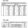
- Figs. 14 , 15(A), and 15(B) show numerical value data of the wide-angle imaging lens of Example 1. More specifically, Fig. 14 shows its basic lens data and Fig. 15(A) shows data relating to the aspherical surfaces. Fig. 15(B) shows data relating to the parameters included in the above-described condition formulae. The numerical value data shown do not include data relating to the optical member 2 such as a cover glass.
- Symbol Di represents the surface interval on the optical axis Z1 between the ith surface and the (i + 1)th surface.
- symbol Si denotes the ith surface as numbered from the object side to the image side, the object-side end surface being denoted by S1.
- both surfaces of each of the second lens L2 and the third lens L3 are aspherical surfaces.
- the values of the radii of curvature of these aspherical surfaces are values of the radii of curvature of their portions close to the optical axis Z1.
- symbol "E” means that the numerical value following it is an exponent of a power having 10 as a base and the numerical value before "E” is multiplied by the power.
- "1.0E-02" means 1.0 x 10 -2 .
- the data of each aspherical surface are values of the coefficients B i and KA of the following Equation (A) representing an aspherical surface. That is, the parameter Z means the length (mm) of the perpendicular from a point on the aspherical surface having a height h as measured from the optical axis Z 1 to the tangential plane to the aspherical surface at its top (the tangential plane is perpendicular to the optical axis Z1).
- Z depth (mm) of a point on the aspherical surface
- h distance (mm) between the point on the aspherical surface and the optical axis Z1 (i.e., height of the point)
- KA conical constant
- R paraxial radius of curvature
- B i ith-order aspherical coefficient.
- Fig. 15(B) shows the values of the parameters included in the above-described condition formulae.
- f is the paraxial focal length (mm) of the entire system
- f1 is the focal length (mm) of the first lens L1
- 2 ⁇ is the diagonal angle of view
- L and BF are the distances shown in Fig. 1 (the thickness of the optical member 2 such as a cover glass is air-converted).
- the parameters of the wide-angle imaging lens of Example 1 fall within the numerical value ranges of the condition formulae.
- Figs. 3-13 are sectional views of wide-angle imaging lenses of Examples 2-12, respectively, which are similar to the wide-angle imaging lens of Example 1.
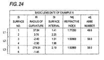
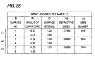
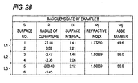
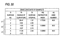
- Figs. 16 , 18 , 20 , 22 , 24 , 26 , 28 , 30 , 32 , 34 , and 36 show basic lens data of the wide-angle imaging lenses of Examples 2-12, respectively.
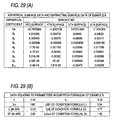
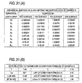
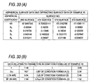
- Figs. 17(A) , 19(A) , 21(A) , 23(A) , 25(A) , 27(A) , 29(A) , 31(A) , 33(A) , 35(A) , and 37(A) show data relating to the aspherical surfaces of the wide-angle imaging lenses of Examples 2-12, respectively.
- 17(B) , 19(B) , 21(B) , 23(B) , 25(B) , 27(B) , 29(B) , 31(B) , 33(B) , 35(B) , and 37(B) show data relating to the parameters included in the above-described condition formulae of the wide-angle imaging lenses of Examples 2-12, respectively.
- the parameters of each of the wide-angle imaging lenses of Examples 2-12 fall within the numerical value ranges of the condition formulae.
- both surfaces of each of the second lens L2 and the third lens L3 of each of the wide-angle imaging lenses of Examples 2-12 are aspherical surfaces.
- the object-side surface of the second lens L2 is shaped in such a manner that it is concave (i.e., recessed) near the optical axis Z1 and its negative power decreases as the position goes away from the optical axis Z1.
- the object-side surface of the second lens L2 is shaped in such a manner as to change from a concave surface (i.e., recessed) to a convex surface (i.e., projected toward the object side) in a peripheral portion.
- the image-side surface of the second lens L2 is shaped in such a manner that it is concave (i.e., recessed) near the optical axis Z1 and its negative power increases as the position goes away from the optical axis Z1.
- the image-side surface of the second lens L2 is shaped in such a manner that it is convex (i.e., projected toward the image side) near the optical axis Z1 and its positive power decreases as the position goes away from the optical axis Z1.
- the image-side surface of the second lens L2 is shaped in such a manner as to change from a convex surface (i.e., projected toward the image side) to a concave surface (i.e., recessed) in a peripheral portion.
- the third lens L3 is made of a polyolefin-type material that is inexpensive and easy to acquire and whose coefficient of water absorption is about 0.01 %.
- the second lens L2 is made of a polyolefin-type material in Examples 1-11 and a polycarbonate-type material in Example 12.
- Figs. 38(A)-38(D) show the spherical aberration, astigmatism, distortion, and lateral color, respectively, of the wide-angle imaging lens of Example 1.
- Each aberration diagram shows an aberration curve(s) at the e-line (wavelength: 546.07 nm) used as a reference wavelength.
- the spherical aberration diagram ( Fig. 38(A) ) and the lateral color diagram ( Fig. 38(D) ) also show aberration curves at the C-line (wavelength: 656.27 nm) and the F-line (wavelength: 486.13 nm).
- a solid-line aberration curve corresponds to the sagittal direction and a broken-line aberration curve corresponds to the tangential direction.
- the parameter ⁇ represents the half angle of view.
- Figs. 39(A)-39(D) show the aberrations of the wide-angle imaging lens of Example 2
- 40(A)-40(D) show the aberrations of the wide-angle imaging lens of Example 3
- 41 (A)-41 (D) show the aberrations of the wide-angle imaging lens of Example 4
- 42(A)-42(D) show the aberrations of the wide-angle imaging lens of Example 5
- 43(A)-43(D) show the aberrations of the wide-angle imaging lens of Example 6
- 44(A)-44(D) show the aberrations of the wide-angle imaging lens of Example 7
- 45(A)-45(D) show the aberrations of the wide-angle imaging lens of Example 8
- 46(A)-46(D) show the aberrations of the wide-angle imaging lens of Example 9
- 47(A)-47(D) show the aberrations of the wide-angle imaging lens of Example 10
- 48(A)-48(D) show the aberrations of the wide
- the invention is not limited to the above embodiment and Examples and various modifications are possible.
- the values of the radii of curvature of the lens surfaces, the surface intervals, the refractive indices of the lenses, etc. are not limited to the values used in the above numerical value Examples and may have other values.
Landscapes
- Physics & Mathematics (AREA)
- General Physics & Mathematics (AREA)
- Optics & Photonics (AREA)
- Lenses (AREA)
- Instruments For Viewing The Inside Of Hollow Bodies (AREA)
Applications Claiming Priority (1)
| Application Number | Priority Date | Filing Date | Title |
|---|---|---|---|
| JP2005306771A JP4841929B2 (ja) | 2005-10-21 | 2005-10-21 | 広角撮像レンズ |
Publications (2)
| Publication Number | Publication Date |
|---|---|
| EP1777941A1 EP1777941A1 (en) | 2007-04-25 |
| EP1777941B1 true EP1777941B1 (en) | 2008-07-23 |
Family
ID=37592943
Family Applications (1)
| Application Number | Title | Priority Date | Filing Date |
|---|---|---|---|
| EP06022048A Not-in-force EP1777941B1 (en) | 2005-10-21 | 2006-10-20 | Wide-angle imaging lens system |
Country Status (8)
| Country | Link |
|---|---|
| US (1) | US7843652B2 (https=) |
| EP (1) | EP1777941B1 (https=) |
| JP (1) | JP4841929B2 (https=) |
| KR (1) | KR100821933B1 (https=) |
| CN (1) | CN100419491C (https=) |
| AT (1) | ATE402564T1 (https=) |
| DE (1) | DE602006001918D1 (https=) |
| TW (1) | TW200717020A (https=) |
Cited By (1)
| Publication number | Priority date | Publication date | Assignee | Title |
|---|---|---|---|---|
| TWI394980B (zh) * | 2010-03-19 | 2013-05-01 | Largan Precision Co Ltd | 攝影用光學鏡組 |
Families Citing this family (31)
| Publication number | Priority date | Publication date | Assignee | Title |
|---|---|---|---|---|
| JP2008102500A (ja) | 2006-09-19 | 2008-05-01 | Fujinon Corp | 撮像レンズ及びこれを備えたカメラ装置 |
| JP5045300B2 (ja) * | 2007-08-07 | 2012-10-10 | 株式会社ニコン | 広角レンズ及びこの広角レンズを有する撮像装置 |
| JP5048474B2 (ja) * | 2007-12-18 | 2012-10-17 | オリンパス株式会社 | 魚眼レンズおよびそれを備えた撮像装置 |
| JP5096226B2 (ja) | 2008-05-16 | 2012-12-12 | パナソニック株式会社 | 広角レンズ |
| JP2010091620A (ja) * | 2008-10-03 | 2010-04-22 | Sony Corp | レンズユニット |
| CN201383032Y (zh) * | 2008-12-16 | 2010-01-13 | 富士能株式会社 | 摄像透镜及使用该摄像透镜的摄像装置 |
| JP5393521B2 (ja) | 2009-03-06 | 2014-01-22 | 富士フイルム株式会社 | 撮像レンズおよび撮像装置 |
| KR101623450B1 (ko) * | 2009-10-13 | 2016-05-23 | 삼성전자주식회사 | 와이드 컨버터 렌즈 |
| US8872887B2 (en) * | 2010-03-05 | 2014-10-28 | Fotonation Limited | Object detection and rendering for wide field of view (WFOV) image acquisition systems |
| KR101118910B1 (ko) | 2010-03-05 | 2012-03-13 | 주식회사 코렌 | 촬영 렌즈 광학계 |
| CN102313967B (zh) * | 2010-06-29 | 2013-07-24 | 比亚迪股份有限公司 | 一种超广角镜头 |
| JPWO2012008312A1 (ja) | 2010-07-14 | 2013-09-09 | オリンパスメディカルシステムズ株式会社 | 対物光学系 |
| JP2012177736A (ja) * | 2011-02-25 | 2012-09-13 | Kyocera Corp | 撮像レンズ |
| US8723959B2 (en) | 2011-03-31 | 2014-05-13 | DigitalOptics Corporation Europe Limited | Face and other object tracking in off-center peripheral regions for nonlinear lens geometries |
| US8493459B2 (en) | 2011-09-15 | 2013-07-23 | DigitalOptics Corporation Europe Limited | Registration of distorted images |
| US8928730B2 (en) | 2012-07-03 | 2015-01-06 | DigitalOptics Corporation Europe Limited | Method and system for correcting a distorted input image |
| JP2014209190A (ja) * | 2013-03-28 | 2014-11-06 | 日本電産サンキョー株式会社 | 広角レンズ |
| CN105793755B (zh) * | 2013-10-30 | 2019-04-30 | 奥林巴斯株式会社 | 摄像装置 |
| US9274322B1 (en) * | 2014-08-21 | 2016-03-01 | Omnivision Technologies, Inc. | Three-piece all-aspheric adapter fisheye lens |
| CN105988201B (zh) * | 2015-04-08 | 2018-09-07 | 浙江舜宇光学有限公司 | 交互式镜头 |
| JP6416070B2 (ja) * | 2015-09-28 | 2018-10-31 | 富士フイルム株式会社 | 撮像レンズおよび撮像レンズを備えた撮像装置 |
| KR102182268B1 (ko) * | 2015-12-09 | 2020-11-25 | (주)탑중앙연구소 | 광각 렌즈 시스템 및 이를 포함하는 광학 장치 |
| EP3457190B1 (en) | 2016-05-12 | 2023-01-11 | Nalux Co. Ltd. | Imaging optical system |
| JP2017207658A (ja) * | 2016-05-19 | 2017-11-24 | オリンパス株式会社 | 撮像装置及びカプセル内視鏡 |
| CN105954859A (zh) * | 2016-07-19 | 2016-09-21 | 黄梅县云泰时代光学仪器有限公司 | 一种广角光学镜头 |
| JP6800640B2 (ja) * | 2016-07-22 | 2020-12-16 | 日本電産サンキョー株式会社 | 広角レンズ |
| JP2018055059A (ja) * | 2016-09-30 | 2018-04-05 | オリンパス株式会社 | 撮像装置 |
| CN106443939B (zh) * | 2016-12-16 | 2019-03-08 | 福建福光天瞳光学有限公司 | 15mm固定结构式无热化红外镜头及其安装方法 |
| JP7117638B2 (ja) * | 2017-03-10 | 2022-08-15 | パナソニックIpマネジメント株式会社 | レンズ系、交換レンズ装置及びカメラシステム |
| KR102206565B1 (ko) * | 2019-06-20 | 2021-01-22 | 한국원자력연구원 | 광각렌즈 시스템 및 이를 구비하는 촬영 시스템 |
| CN112799212A (zh) * | 2021-01-26 | 2021-05-14 | 深圳阜时科技有限公司 | 镜头系统、光学感测装置和电子设备 |
Citations (2)
| Publication number | Priority date | Publication date | Assignee | Title |
|---|---|---|---|---|
| US20060171042A1 (en) * | 2005-01-31 | 2006-08-03 | Konica Minolta Opto, Inc. | Wide-angle lens system |
| EP1724622A2 (en) * | 2003-07-11 | 2006-11-22 | Konica Minolta Opto, Inc. | Image pick-up lens, image pick-up unit, and mobile terminal provided with this image pick-up unit |
Family Cites Families (28)
| Publication number | Priority date | Publication date | Assignee | Title |
|---|---|---|---|---|
| JPH0772382A (ja) * | 1993-09-02 | 1995-03-17 | Nisshin Koki Kk | 広角レンズ |
| JP3380037B2 (ja) * | 1994-05-31 | 2003-02-24 | ペンタックス株式会社 | 後絞り型トリプレットレンズ系 |
| JPH10104509A (ja) * | 1996-09-30 | 1998-04-24 | Matsushita Electric Ind Co Ltd | 広角レンズ群 |
| JPH10115777A (ja) * | 1996-10-11 | 1998-05-06 | Olympus Optical Co Ltd | 撮影レンズ |
| US5875059A (en) * | 1997-02-19 | 1999-02-23 | Eastman Kodak Company | Variable focal length lens system having a divergent front lens unit |
| JP3295027B2 (ja) | 1997-10-17 | 2002-06-24 | 株式会社マーク | レトロフォーカス型大口径比広角レンズ |
| JP3505980B2 (ja) * | 1997-10-20 | 2004-03-15 | ミノルタ株式会社 | 撮像装置 |
| JP2001033689A (ja) * | 1999-07-26 | 2001-02-09 | Fuji Photo Optical Co Ltd | 明るく広角な赤外線レンズ |
| JP4268323B2 (ja) | 2000-03-23 | 2009-05-27 | 株式会社長野光学研究所 | 広角レンズ |
| JP4674407B2 (ja) | 2000-04-11 | 2011-04-20 | 株式会社ニコン | ワイドコンバーターレンズ |
| JP3433733B2 (ja) * | 2000-07-03 | 2003-08-04 | ミノルタ株式会社 | 撮像レンズ装置 |
| JP4700821B2 (ja) | 2001-02-21 | 2011-06-15 | マクセルファインテック株式会社 | 広角レンズ |
| JP4727056B2 (ja) | 2001-03-27 | 2011-07-20 | 富士フイルム株式会社 | 画像読取用レンズ |
| JP2003195161A (ja) * | 2001-12-21 | 2003-07-09 | Kyocera Corp | 超広角レンズ |
| US7110188B2 (en) * | 2003-05-27 | 2006-09-19 | Konica Minolta Opto, Inc. | Small imaging lens and imaging apparatus |
| JP4197994B2 (ja) * | 2003-06-19 | 2008-12-17 | コニカミノルタオプト株式会社 | 撮像装置 |
| JP2005181596A (ja) * | 2003-12-18 | 2005-07-07 | Nagano Kogaku Kenkyusho:Kk | 広角レンズ |
| JP2005227755A (ja) * | 2004-01-13 | 2005-08-25 | Miyota Kk | 小型結像レンズ |
| JP3938143B2 (ja) * | 2004-02-09 | 2007-06-27 | コニカミノルタオプト株式会社 | 超広角光学系 |
| JP2005258180A (ja) | 2004-03-12 | 2005-09-22 | Seiko Epson Corp | 広角撮像レンズ及びカメラモジュール |
| JP2005258181A (ja) | 2004-03-12 | 2005-09-22 | Seiko Epson Corp | 撮像レンズ及びカメラモジュール |
| JP2005321742A (ja) * | 2004-05-10 | 2005-11-17 | Hideaki Ishizuki | 超広角高解像度レンズ |
| JP2006119368A (ja) * | 2004-10-21 | 2006-05-11 | Konica Minolta Opto Inc | 広角光学系、撮像レンズ装置、モニタカメラ及びデジタル機器 |
| JP2006126418A (ja) | 2004-10-28 | 2006-05-18 | Nidec Copal Corp | ズームレンズ |
| JP2006162829A (ja) | 2004-12-06 | 2006-06-22 | Seiko Epson Corp | 広角撮像レンズ及び撮像装置 |
| JP2006184385A (ja) | 2004-12-27 | 2006-07-13 | Seiko Epson Corp | 広角撮像レンズ |
| JP4847150B2 (ja) * | 2005-02-21 | 2011-12-28 | 富士フイルム株式会社 | 広角撮像レンズ |
| JP4747645B2 (ja) * | 2005-04-11 | 2011-08-17 | コニカミノルタオプト株式会社 | 広角レンズ、及び、撮像装置 |
-
2005
- 2005-10-21 JP JP2005306771A patent/JP4841929B2/ja not_active Expired - Fee Related
-
2006
- 2006-10-18 KR KR1020060101341A patent/KR100821933B1/ko not_active Expired - Fee Related
- 2006-10-19 US US11/583,110 patent/US7843652B2/en not_active Expired - Fee Related
- 2006-10-20 DE DE602006001918T patent/DE602006001918D1/de active Active
- 2006-10-20 EP EP06022048A patent/EP1777941B1/en not_active Not-in-force
- 2006-10-20 TW TW095138761A patent/TW200717020A/zh not_active IP Right Cessation
- 2006-10-20 CN CNB2006101356555A patent/CN100419491C/zh not_active Expired - Fee Related
- 2006-10-20 AT AT06022048T patent/ATE402564T1/de not_active IP Right Cessation
Patent Citations (2)
| Publication number | Priority date | Publication date | Assignee | Title |
|---|---|---|---|---|
| EP1724622A2 (en) * | 2003-07-11 | 2006-11-22 | Konica Minolta Opto, Inc. | Image pick-up lens, image pick-up unit, and mobile terminal provided with this image pick-up unit |
| US20060171042A1 (en) * | 2005-01-31 | 2006-08-03 | Konica Minolta Opto, Inc. | Wide-angle lens system |
Cited By (1)
| Publication number | Priority date | Publication date | Assignee | Title |
|---|---|---|---|---|
| TWI394980B (zh) * | 2010-03-19 | 2013-05-01 | Largan Precision Co Ltd | 攝影用光學鏡組 |
Also Published As
| Publication number | Publication date |
|---|---|
| US20070091458A1 (en) | 2007-04-26 |
| TW200717020A (en) | 2007-05-01 |
| KR20070043622A (ko) | 2007-04-25 |
| JP4841929B2 (ja) | 2011-12-21 |
| JP2007114546A (ja) | 2007-05-10 |
| KR100821933B1 (ko) | 2008-04-15 |
| TWI320486B (https=) | 2010-02-11 |
| DE602006001918D1 (de) | 2008-09-04 |
| EP1777941A1 (en) | 2007-04-25 |
| US7843652B2 (en) | 2010-11-30 |
| CN1952723A (zh) | 2007-04-25 |
| ATE402564T1 (de) | 2008-08-15 |
| CN100419491C (zh) | 2008-09-17 |
Similar Documents
| Publication | Publication Date | Title |
|---|---|---|
| EP1777941B1 (en) | Wide-angle imaging lens system | |
| EP1777569B1 (en) | Wide-angle imaging lens | |
| US7408725B2 (en) | Single focus lens | |
| US7957074B2 (en) | Imaging lens system and imaging apparatus using the imaging lens system | |
| JP5330202B2 (ja) | 撮像レンズおよび撮像装置 | |
| US7518809B2 (en) | Ultra wide-angle imaging lens device and imaging apparatus | |
| CN201503514U (zh) | 摄像透镜及使用该摄像透镜的摄像装置 | |
| EP1821129B1 (en) | Imaging lens | |
| JP5252842B2 (ja) | 撮像レンズ | |
| JP7748200B2 (ja) | 撮像レンズ系及び撮像装置 | |
| JP5084335B2 (ja) | 撮像レンズ | |
| US8508862B2 (en) | Image pickup lens and image pickup apparatus | |
| JP5450023B2 (ja) | 撮像レンズおよびこの撮像レンズを用いた撮像装置 | |
| JP2010160479A (ja) | 撮像レンズおよびこの撮像レンズを用いた撮像装置 | |
| JP5689480B2 (ja) | 撮像レンズおよび撮像装置 | |
| JP2008102500A (ja) | 撮像レンズ及びこれを備えたカメラ装置 | |
| JP5568732B2 (ja) | 撮像レンズ | |
| JP7531659B2 (ja) | 撮像レンズ系及び撮像装置 | |
| EP4137860B1 (en) | Optical imaging lens | |
| JP6818832B2 (ja) | 撮像レンズ系及び撮像装置 | |
| CN101149464A (zh) | 摄像透镜及具备此的摄像机装置 | |
| JP7100111B2 (ja) | 撮像レンズ系及び撮像装置 | |
| JP7295312B2 (ja) | 撮像レンズ系及び撮像装置 | |
| JP2024146579A (ja) | 撮像レンズ、撮像装置及び移動体 | |
| JP2024146583A (ja) | 撮像レンズ、撮像装置及び移動体 |
Legal Events
| Date | Code | Title | Description |
|---|---|---|---|
| PUAI | Public reference made under article 153(3) epc to a published international application that has entered the european phase |
Free format text: ORIGINAL CODE: 0009012 |
|
| 17P | Request for examination filed |
Effective date: 20061020 |
|
| AK | Designated contracting states |
Kind code of ref document: A1 Designated state(s): AT BE BG CH CY CZ DE DK EE ES FI FR GB GR HU IE IS IT LI LT LU LV MC NL PL PT RO SE SI SK TR |
|
| AX | Request for extension of the european patent |
Extension state: AL BA HR MK YU |
|
| AKX | Designation fees paid |
Designated state(s): AT BE BG CH CY CZ DE DK EE ES FI FR GB GR HU IE IS IT LI LT LU LV MC NL PL PT RO SE SI SK TR |
|
| GRAP | Despatch of communication of intention to grant a patent |
Free format text: ORIGINAL CODE: EPIDOSNIGR1 |
|
| GRAS | Grant fee paid |
Free format text: ORIGINAL CODE: EPIDOSNIGR3 |
|
| GRAA | (expected) grant |
Free format text: ORIGINAL CODE: 0009210 |
|
| AK | Designated contracting states |
Kind code of ref document: B1 Designated state(s): AT BE BG CH CY CZ DE DK EE ES FI FR GB GR HU IE IS IT LI LT LU LV MC NL PL PT RO SE SI SK TR |
|
| REG | Reference to a national code |
Ref country code: GB Ref legal event code: FG4D |
|
| REG | Reference to a national code |
Ref country code: CH Ref legal event code: EP |
|
| REG | Reference to a national code |
Ref country code: IE Ref legal event code: FG4D |
|
| REF | Corresponds to: |
Ref document number: 602006001918 Country of ref document: DE Date of ref document: 20080904 Kind code of ref document: P |
|
| NLV1 | Nl: lapsed or annulled due to failure to fulfill the requirements of art. 29p and 29m of the patents act | ||
| PG25 | Lapsed in a contracting state [announced via postgrant information from national office to epo] |
Ref country code: LT Free format text: LAPSE BECAUSE OF FAILURE TO SUBMIT A TRANSLATION OF THE DESCRIPTION OR TO PAY THE FEE WITHIN THE PRESCRIBED TIME-LIMIT Effective date: 20080723 Ref country code: IS Free format text: LAPSE BECAUSE OF FAILURE TO SUBMIT A TRANSLATION OF THE DESCRIPTION OR TO PAY THE FEE WITHIN THE PRESCRIBED TIME-LIMIT Effective date: 20081123 Ref country code: NL Free format text: LAPSE BECAUSE OF FAILURE TO SUBMIT A TRANSLATION OF THE DESCRIPTION OR TO PAY THE FEE WITHIN THE PRESCRIBED TIME-LIMIT Effective date: 20080723 |
|
| PG25 | Lapsed in a contracting state [announced via postgrant information from national office to epo] |
Ref country code: PT Free format text: LAPSE BECAUSE OF FAILURE TO SUBMIT A TRANSLATION OF THE DESCRIPTION OR TO PAY THE FEE WITHIN THE PRESCRIBED TIME-LIMIT Effective date: 20081223 Ref country code: BG Free format text: LAPSE BECAUSE OF FAILURE TO SUBMIT A TRANSLATION OF THE DESCRIPTION OR TO PAY THE FEE WITHIN THE PRESCRIBED TIME-LIMIT Effective date: 20081023 Ref country code: ES Free format text: LAPSE BECAUSE OF FAILURE TO SUBMIT A TRANSLATION OF THE DESCRIPTION OR TO PAY THE FEE WITHIN THE PRESCRIBED TIME-LIMIT Effective date: 20081103 Ref country code: SI Free format text: LAPSE BECAUSE OF FAILURE TO SUBMIT A TRANSLATION OF THE DESCRIPTION OR TO PAY THE FEE WITHIN THE PRESCRIBED TIME-LIMIT Effective date: 20080723 Ref country code: AT Free format text: LAPSE BECAUSE OF FAILURE TO SUBMIT A TRANSLATION OF THE DESCRIPTION OR TO PAY THE FEE WITHIN THE PRESCRIBED TIME-LIMIT Effective date: 20080723 Ref country code: FI Free format text: LAPSE BECAUSE OF FAILURE TO SUBMIT A TRANSLATION OF THE DESCRIPTION OR TO PAY THE FEE WITHIN THE PRESCRIBED TIME-LIMIT Effective date: 20080723 Ref country code: LV Free format text: LAPSE BECAUSE OF FAILURE TO SUBMIT A TRANSLATION OF THE DESCRIPTION OR TO PAY THE FEE WITHIN THE PRESCRIBED TIME-LIMIT Effective date: 20080723 |
|
| PG25 | Lapsed in a contracting state [announced via postgrant information from national office to epo] |
Ref country code: BE Free format text: LAPSE BECAUSE OF FAILURE TO SUBMIT A TRANSLATION OF THE DESCRIPTION OR TO PAY THE FEE WITHIN THE PRESCRIBED TIME-LIMIT Effective date: 20080723 |
|
| PG25 | Lapsed in a contracting state [announced via postgrant information from national office to epo] |
Ref country code: DK Free format text: LAPSE BECAUSE OF FAILURE TO SUBMIT A TRANSLATION OF THE DESCRIPTION OR TO PAY THE FEE WITHIN THE PRESCRIBED TIME-LIMIT Effective date: 20080723 Ref country code: EE Free format text: LAPSE BECAUSE OF FAILURE TO SUBMIT A TRANSLATION OF THE DESCRIPTION OR TO PAY THE FEE WITHIN THE PRESCRIBED TIME-LIMIT Effective date: 20080723 |
|
| PG25 | Lapsed in a contracting state [announced via postgrant information from national office to epo] |
Ref country code: SK Free format text: LAPSE BECAUSE OF FAILURE TO SUBMIT A TRANSLATION OF THE DESCRIPTION OR TO PAY THE FEE WITHIN THE PRESCRIBED TIME-LIMIT Effective date: 20080723 Ref country code: CZ Free format text: LAPSE BECAUSE OF FAILURE TO SUBMIT A TRANSLATION OF THE DESCRIPTION OR TO PAY THE FEE WITHIN THE PRESCRIBED TIME-LIMIT Effective date: 20080723 Ref country code: RO Free format text: LAPSE BECAUSE OF FAILURE TO SUBMIT A TRANSLATION OF THE DESCRIPTION OR TO PAY THE FEE WITHIN THE PRESCRIBED TIME-LIMIT Effective date: 20080723 Ref country code: MC Free format text: LAPSE BECAUSE OF NON-PAYMENT OF DUE FEES Effective date: 20081031 |
|
| PLBE | No opposition filed within time limit |
Free format text: ORIGINAL CODE: 0009261 |
|
| STAA | Information on the status of an ep patent application or granted ep patent |
Free format text: STATUS: NO OPPOSITION FILED WITHIN TIME LIMIT |
|
| 26N | No opposition filed |
Effective date: 20090424 |
|
| PG25 | Lapsed in a contracting state [announced via postgrant information from national office to epo] |
Ref country code: IT Free format text: LAPSE BECAUSE OF FAILURE TO SUBMIT A TRANSLATION OF THE DESCRIPTION OR TO PAY THE FEE WITHIN THE PRESCRIBED TIME-LIMIT Effective date: 20080723 |
|
| PG25 | Lapsed in a contracting state [announced via postgrant information from national office to epo] |
Ref country code: IE Free format text: LAPSE BECAUSE OF NON-PAYMENT OF DUE FEES Effective date: 20081020 |
|
| PG25 | Lapsed in a contracting state [announced via postgrant information from national office to epo] |
Ref country code: SE Free format text: LAPSE BECAUSE OF FAILURE TO SUBMIT A TRANSLATION OF THE DESCRIPTION OR TO PAY THE FEE WITHIN THE PRESCRIBED TIME-LIMIT Effective date: 20081023 |
|
| PG25 | Lapsed in a contracting state [announced via postgrant information from national office to epo] |
Ref country code: PL Free format text: LAPSE BECAUSE OF FAILURE TO SUBMIT A TRANSLATION OF THE DESCRIPTION OR TO PAY THE FEE WITHIN THE PRESCRIBED TIME-LIMIT Effective date: 20080723 |
|
| PG25 | Lapsed in a contracting state [announced via postgrant information from national office to epo] |
Ref country code: CY Free format text: LAPSE BECAUSE OF FAILURE TO SUBMIT A TRANSLATION OF THE DESCRIPTION OR TO PAY THE FEE WITHIN THE PRESCRIBED TIME-LIMIT Effective date: 20080723 Ref country code: HU Free format text: LAPSE BECAUSE OF FAILURE TO SUBMIT A TRANSLATION OF THE DESCRIPTION OR TO PAY THE FEE WITHIN THE PRESCRIBED TIME-LIMIT Effective date: 20090124 Ref country code: LU Free format text: LAPSE BECAUSE OF NON-PAYMENT OF DUE FEES Effective date: 20081020 |
|
| PG25 | Lapsed in a contracting state [announced via postgrant information from national office to epo] |
Ref country code: TR Free format text: LAPSE BECAUSE OF FAILURE TO SUBMIT A TRANSLATION OF THE DESCRIPTION OR TO PAY THE FEE WITHIN THE PRESCRIBED TIME-LIMIT Effective date: 20080723 |
|
| PG25 | Lapsed in a contracting state [announced via postgrant information from national office to epo] |
Ref country code: GR Free format text: LAPSE BECAUSE OF FAILURE TO SUBMIT A TRANSLATION OF THE DESCRIPTION OR TO PAY THE FEE WITHIN THE PRESCRIBED TIME-LIMIT Effective date: 20081024 |
|
| REG | Reference to a national code |
Ref country code: CH Ref legal event code: PL |
|
| PG25 | Lapsed in a contracting state [announced via postgrant information from national office to epo] |
Ref country code: LI Free format text: LAPSE BECAUSE OF NON-PAYMENT OF DUE FEES Effective date: 20101031 Ref country code: CH Free format text: LAPSE BECAUSE OF NON-PAYMENT OF DUE FEES Effective date: 20101031 |
|
| PGFP | Annual fee paid to national office [announced via postgrant information from national office to epo] |
Ref country code: FR Payment date: 20121018 Year of fee payment: 7 |
|
| PGFP | Annual fee paid to national office [announced via postgrant information from national office to epo] |
Ref country code: GB Payment date: 20121017 Year of fee payment: 7 |
|
| GBPC | Gb: european patent ceased through non-payment of renewal fee |
Effective date: 20131020 |
|
| PG25 | Lapsed in a contracting state [announced via postgrant information from national office to epo] |
Ref country code: GB Free format text: LAPSE BECAUSE OF NON-PAYMENT OF DUE FEES Effective date: 20131020 |
|
| REG | Reference to a national code |
Ref country code: FR Ref legal event code: ST Effective date: 20140630 |
|
| PG25 | Lapsed in a contracting state [announced via postgrant information from national office to epo] |
Ref country code: FR Free format text: LAPSE BECAUSE OF NON-PAYMENT OF DUE FEES Effective date: 20131031 |
|
| REG | Reference to a national code |
Ref country code: DE Ref legal event code: R082 Ref document number: 602006001918 Country of ref document: DE Representative=s name: MANITZ FINSTERWALD PATENTANWAELTE PARTMBB, DE Ref country code: DE Ref legal event code: R082 Ref document number: 602006001918 Country of ref document: DE Representative=s name: MANITZ FINSTERWALD PATENT- UND RECHTSANWALTSPA, DE Ref country code: DE Ref legal event code: R082 Ref document number: 602006001918 Country of ref document: DE Representative=s name: KLUNKER IP PATENTANWAELTE PARTG MBB, DE |
|
| REG | Reference to a national code |
Ref country code: DE Ref legal event code: R081 Ref document number: 602006001918 Country of ref document: DE Owner name: NANCHANG O-FILM OPTICAL-ELECTRONIC TECH CO., L, CN Free format text: FORMER OWNER: FUJINON CORPORATION, SAITAMA, JP Ref country code: DE Ref legal event code: R082 Ref document number: 602006001918 Country of ref document: DE Representative=s name: MANITZ FINSTERWALD PATENTANWAELTE PARTMBB, DE Ref country code: DE Ref legal event code: R082 Ref document number: 602006001918 Country of ref document: DE Representative=s name: MANITZ FINSTERWALD PATENT- UND RECHTSANWALTSPA, DE Ref country code: DE Ref legal event code: R081 Ref document number: 602006001918 Country of ref document: DE Owner name: TIANJIN O-FILM OPTO ELECTRONICS CO., LTD., CN Free format text: FORMER OWNER: FUJINON CORPORATION, SAITAMA, JP Ref country code: DE Ref legal event code: R082 Ref document number: 602006001918 Country of ref document: DE Representative=s name: KLUNKER IP PATENTANWAELTE PARTG MBB, DE Ref country code: DE Ref legal event code: R081 Ref document number: 602006001918 Country of ref document: DE Owner name: FUJIFILM CORPORATION, JP Free format text: FORMER OWNER: FUJINON CORPORATION, SAITAMA, JP |
|
| REG | Reference to a national code |
Ref country code: DE Ref legal event code: R082 Ref document number: 602006001918 Country of ref document: DE Representative=s name: MANITZ FINSTERWALD PATENTANWAELTE PARTMBB, DE Ref country code: DE Ref legal event code: R081 Ref document number: 602006001918 Country of ref document: DE Owner name: NANCHANG O-FILM OPTICAL-ELECTRONIC TECH CO., L, CN Free format text: FORMER OWNER: FUJIFILM CORPORATION, TOKYO, JP Ref country code: DE Ref legal event code: R082 Ref document number: 602006001918 Country of ref document: DE Representative=s name: MANITZ FINSTERWALD PATENT- UND RECHTSANWALTSPA, DE Ref country code: DE Ref legal event code: R081 Ref document number: 602006001918 Country of ref document: DE Owner name: TIANJIN O-FILM OPTO ELECTRONICS CO., LTD., CN Free format text: FORMER OWNER: FUJIFILM CORPORATION, TOKYO, JP |
|
| REG | Reference to a national code |
Ref country code: DE Ref legal event code: R082 Ref document number: 602006001918 Country of ref document: DE Representative=s name: MANITZ FINSTERWALD PATENT- UND RECHTSANWALTSPA, DE Ref country code: DE Ref legal event code: R081 Ref document number: 602006001918 Country of ref document: DE Owner name: TIANJIN O-FILM OPTO ELECTRONICS CO., LTD., CN Free format text: FORMER OWNER: NANCHANG O-FILM OPTICAL-ELECTRONIC TECH CO., LTD., JIANGXI, CN |
|
| PGFP | Annual fee paid to national office [announced via postgrant information from national office to epo] |
Ref country code: DE Payment date: 20211020 Year of fee payment: 16 |
|
| REG | Reference to a national code |
Ref country code: DE Ref legal event code: R079 Ref document number: 602006001918 Country of ref document: DE Free format text: PREVIOUS MAIN CLASS: H04N0005225000 Ipc: H04N0023000000 |
|
| REG | Reference to a national code |
Ref country code: DE Ref legal event code: R119 Ref document number: 602006001918 Country of ref document: DE |
|
| PG25 | Lapsed in a contracting state [announced via postgrant information from national office to epo] |
Ref country code: DE Free format text: LAPSE BECAUSE OF NON-PAYMENT OF DUE FEES Effective date: 20230503 |