EP1721031B1 - Verringerung von karottendefekten bei der siliciumcarbid-epitaxie - Google Patents
Verringerung von karottendefekten bei der siliciumcarbid-epitaxie Download PDFInfo
- Publication number
- EP1721031B1 EP1721031B1 EP04811590A EP04811590A EP1721031B1 EP 1721031 B1 EP1721031 B1 EP 1721031B1 EP 04811590 A EP04811590 A EP 04811590A EP 04811590 A EP04811590 A EP 04811590A EP 1721031 B1 EP1721031 B1 EP 1721031B1
- Authority
- EP
- European Patent Office
- Prior art keywords
- layer
- silicon carbide
- epitaxial
- substrate
- growth
- Prior art date
- Legal status (The legal status is an assumption and is not a legal conclusion. Google has not performed a legal analysis and makes no representation as to the accuracy of the status listed.)
- Active
Links
- 230000007547 defect Effects 0.000 title claims abstract description 115
- HBMJWWWQQXIZIP-UHFFFAOYSA-N silicon carbide Chemical compound [Si+]#[C-] HBMJWWWQQXIZIP-UHFFFAOYSA-N 0.000 title claims abstract description 101
- 229910010271 silicon carbide Inorganic materials 0.000 title claims abstract description 98
- 244000000626 Daucus carota Species 0.000 title claims abstract description 84
- 235000002767 Daucus carota Nutrition 0.000 title claims abstract description 84
- 230000009467 reduction Effects 0.000 title description 6
- 238000000407 epitaxy Methods 0.000 title description 3
- 238000000034 method Methods 0.000 claims abstract description 80
- 239000000758 substrate Substances 0.000 claims abstract description 77
- 238000005530 etching Methods 0.000 claims abstract description 26
- 239000004065 semiconductor Substances 0.000 claims abstract description 9
- 229910021421 monocrystalline silicon Inorganic materials 0.000 claims abstract description 4
- 230000006911 nucleation Effects 0.000 claims abstract description 3
- 238000010899 nucleation Methods 0.000 claims abstract description 3
- 239000007789 gas Substances 0.000 claims description 57
- ATUOYWHBWRKTHZ-UHFFFAOYSA-N Propane Chemical compound CCC ATUOYWHBWRKTHZ-UHFFFAOYSA-N 0.000 claims description 16
- OKTJSMMVPCPJKN-UHFFFAOYSA-N Carbon Chemical compound [C] OKTJSMMVPCPJKN-UHFFFAOYSA-N 0.000 claims description 11
- 239000001294 propane Substances 0.000 claims description 8
- 229910052799 carbon Inorganic materials 0.000 claims description 7
- 229910052710 silicon Inorganic materials 0.000 claims description 6
- 239000010703 silicon Substances 0.000 claims description 6
- IJGRMHOSHXDMSA-UHFFFAOYSA-N Atomic nitrogen Chemical compound N#N IJGRMHOSHXDMSA-UHFFFAOYSA-N 0.000 claims description 4
- 239000002019 doping agent Substances 0.000 claims description 4
- ZOXJGFHDIHLPTG-UHFFFAOYSA-N Boron Chemical compound [B] ZOXJGFHDIHLPTG-UHFFFAOYSA-N 0.000 claims description 2
- OAICVXFJPJFONN-UHFFFAOYSA-N Phosphorus Chemical compound [P] OAICVXFJPJFONN-UHFFFAOYSA-N 0.000 claims description 2
- XAGFODPZIPBFFR-UHFFFAOYSA-N aluminium Chemical compound [Al] XAGFODPZIPBFFR-UHFFFAOYSA-N 0.000 claims description 2
- 229910052782 aluminium Inorganic materials 0.000 claims description 2
- 229910052796 boron Inorganic materials 0.000 claims description 2
- 238000004519 manufacturing process Methods 0.000 claims description 2
- 229910052757 nitrogen Inorganic materials 0.000 claims description 2
- 229910052698 phosphorus Inorganic materials 0.000 claims description 2
- 239000011574 phosphorus Substances 0.000 claims description 2
- 239000004411 aluminium Substances 0.000 claims 1
- 230000008569 process Effects 0.000 abstract description 50
- 208000031481 Pathologic Constriction Diseases 0.000 abstract 1
- 238000000151 deposition Methods 0.000 description 27
- 230000008021 deposition Effects 0.000 description 23
- 239000013078 crystal Substances 0.000 description 19
- 235000012431 wafers Nutrition 0.000 description 19
- 238000006243 chemical reaction Methods 0.000 description 16
- 238000005229 chemical vapour deposition Methods 0.000 description 16
- 239000000463 material Substances 0.000 description 12
- 230000000877 morphologic effect Effects 0.000 description 9
- 238000002474 experimental method Methods 0.000 description 8
- BLRPTPMANUNPDV-UHFFFAOYSA-N Silane Chemical compound [SiH4] BLRPTPMANUNPDV-UHFFFAOYSA-N 0.000 description 7
- 239000012159 carrier gas Substances 0.000 description 6
- 239000003153 chemical reaction reagent Substances 0.000 description 5
- 238000010438 heat treatment Methods 0.000 description 5
- 238000001000 micrograph Methods 0.000 description 5
- 238000012986 modification Methods 0.000 description 5
- 230000004048 modification Effects 0.000 description 5
- 239000000376 reactant Substances 0.000 description 5
- 229910000077 silane Inorganic materials 0.000 description 5
- 239000010439 graphite Substances 0.000 description 4
- 229910002804 graphite Inorganic materials 0.000 description 4
- 230000008901 benefit Effects 0.000 description 3
- 230000015556 catabolic process Effects 0.000 description 3
- 238000011065 in-situ storage Methods 0.000 description 3
- 230000007246 mechanism Effects 0.000 description 3
- 230000036961 partial effect Effects 0.000 description 3
- 230000001902 propagating effect Effects 0.000 description 3
- UFHFLCQGNIYNRP-UHFFFAOYSA-N Hydrogen Chemical compound [H][H] UFHFLCQGNIYNRP-UHFFFAOYSA-N 0.000 description 2
- 230000015572 biosynthetic process Effects 0.000 description 2
- 230000002939 deleterious effect Effects 0.000 description 2
- 230000001419 dependent effect Effects 0.000 description 2
- 238000005137 deposition process Methods 0.000 description 2
- 238000010586 diagram Methods 0.000 description 2
- 230000000694 effects Effects 0.000 description 2
- 230000001939 inductive effect Effects 0.000 description 2
- 238000004943 liquid phase epitaxy Methods 0.000 description 2
- 238000000623 plasma-assisted chemical vapour deposition Methods 0.000 description 2
- 239000010453 quartz Substances 0.000 description 2
- 238000011160 research Methods 0.000 description 2
- VYPSYNLAJGMNEJ-UHFFFAOYSA-N silicon dioxide Inorganic materials O=[Si]=O VYPSYNLAJGMNEJ-UHFFFAOYSA-N 0.000 description 2
- 239000007787 solid Substances 0.000 description 2
- 238000000927 vapour-phase epitaxy Methods 0.000 description 2
- XUIMIQQOPSSXEZ-UHFFFAOYSA-N Silicon Chemical compound [Si] XUIMIQQOPSSXEZ-UHFFFAOYSA-N 0.000 description 1
- 229910045601 alloy Inorganic materials 0.000 description 1
- 239000000956 alloy Substances 0.000 description 1
- 230000000903 blocking effect Effects 0.000 description 1
- 239000006227 byproduct Substances 0.000 description 1
- 239000000969 carrier Substances 0.000 description 1
- 150000001875 compounds Chemical class 0.000 description 1
- 238000011109 contamination Methods 0.000 description 1
- 230000001627 detrimental effect Effects 0.000 description 1
- 238000001152 differential interference contrast microscopy Methods 0.000 description 1
- 238000011066 ex-situ storage Methods 0.000 description 1
- 229910052732 germanium Inorganic materials 0.000 description 1
- GNPVGFCGXDBREM-UHFFFAOYSA-N germanium atom Chemical compound [Ge] GNPVGFCGXDBREM-UHFFFAOYSA-N 0.000 description 1
- 239000001257 hydrogen Substances 0.000 description 1
- 229910052739 hydrogen Inorganic materials 0.000 description 1
- 238000003384 imaging method Methods 0.000 description 1
- 230000001976 improved effect Effects 0.000 description 1
- 230000006698 induction Effects 0.000 description 1
- 230000000977 initiatory effect Effects 0.000 description 1
- 150000004767 nitrides Chemical class 0.000 description 1
- 230000003287 optical effect Effects 0.000 description 1
- 239000002243 precursor Substances 0.000 description 1
- 230000000644 propagated effect Effects 0.000 description 1
- 230000005855 radiation Effects 0.000 description 1
- 229910052594 sapphire Inorganic materials 0.000 description 1
- 239000010980 sapphire Substances 0.000 description 1
- 229920006395 saturated elastomer Polymers 0.000 description 1
- 241000894007 species Species 0.000 description 1
- 238000004627 transmission electron microscopy Methods 0.000 description 1
Images


Classifications
-
- C—CHEMISTRY; METALLURGY
- C30—CRYSTAL GROWTH
- C30B—SINGLE-CRYSTAL GROWTH; UNIDIRECTIONAL SOLIDIFICATION OF EUTECTIC MATERIAL OR UNIDIRECTIONAL DEMIXING OF EUTECTOID MATERIAL; REFINING BY ZONE-MELTING OF MATERIAL; PRODUCTION OF A HOMOGENEOUS POLYCRYSTALLINE MATERIAL WITH DEFINED STRUCTURE; SINGLE CRYSTALS OR HOMOGENEOUS POLYCRYSTALLINE MATERIAL WITH DEFINED STRUCTURE; AFTER-TREATMENT OF SINGLE CRYSTALS OR A HOMOGENEOUS POLYCRYSTALLINE MATERIAL WITH DEFINED STRUCTURE; APPARATUS THEREFOR
- C30B25/00—Single-crystal growth by chemical reaction of reactive gases, e.g. chemical vapour-deposition growth
- C30B25/02—Epitaxial-layer growth
-
- C—CHEMISTRY; METALLURGY
- C30—CRYSTAL GROWTH
- C30B—SINGLE-CRYSTAL GROWTH; UNIDIRECTIONAL SOLIDIFICATION OF EUTECTIC MATERIAL OR UNIDIRECTIONAL DEMIXING OF EUTECTOID MATERIAL; REFINING BY ZONE-MELTING OF MATERIAL; PRODUCTION OF A HOMOGENEOUS POLYCRYSTALLINE MATERIAL WITH DEFINED STRUCTURE; SINGLE CRYSTALS OR HOMOGENEOUS POLYCRYSTALLINE MATERIAL WITH DEFINED STRUCTURE; AFTER-TREATMENT OF SINGLE CRYSTALS OR A HOMOGENEOUS POLYCRYSTALLINE MATERIAL WITH DEFINED STRUCTURE; APPARATUS THEREFOR
- C30B29/00—Single crystals or homogeneous polycrystalline material with defined structure characterised by the material or by their shape
- C30B29/10—Inorganic compounds or compositions
- C30B29/36—Carbides
-
- C—CHEMISTRY; METALLURGY
- C03—GLASS; MINERAL OR SLAG WOOL
- C03B—MANUFACTURE, SHAPING, OR SUPPLEMENTARY PROCESSES
- C03B23/00—Re-forming shaped glass
- C03B23/02—Re-forming glass sheets
-
- H—ELECTRICITY
- H01—ELECTRIC ELEMENTS
- H01L—SEMICONDUCTOR DEVICES NOT COVERED BY CLASS H10
- H01L21/00—Processes or apparatus adapted for the manufacture or treatment of semiconductor or solid state devices or of parts thereof
- H01L21/02—Manufacture or treatment of semiconductor devices or of parts thereof
- H01L21/02002—Preparing wafers
- H01L21/02005—Preparing bulk and homogeneous wafers
- H01L21/02008—Multistep processes
- H01L21/0201—Specific process step
- H01L21/02019—Chemical etching
-
- H—ELECTRICITY
- H01—ELECTRIC ELEMENTS
- H01L—SEMICONDUCTOR DEVICES NOT COVERED BY CLASS H10
- H01L21/00—Processes or apparatus adapted for the manufacture or treatment of semiconductor or solid state devices or of parts thereof
- H01L21/02—Manufacture or treatment of semiconductor devices or of parts thereof
- H01L21/04—Manufacture or treatment of semiconductor devices or of parts thereof the devices having at least one potential-jump barrier or surface barrier, e.g. PN junction, depletion layer or carrier concentration layer
- H01L21/18—Manufacture or treatment of semiconductor devices or of parts thereof the devices having at least one potential-jump barrier or surface barrier, e.g. PN junction, depletion layer or carrier concentration layer the devices having semiconductor bodies comprising elements of Group IV of the Periodic System or AIIIBV compounds with or without impurities, e.g. doping materials
- H01L21/30—Treatment of semiconductor bodies using processes or apparatus not provided for in groups H01L21/20 - H01L21/26
- H01L21/302—Treatment of semiconductor bodies using processes or apparatus not provided for in groups H01L21/20 - H01L21/26 to change their surface-physical characteristics or shape, e.g. etching, polishing, cutting
- H01L21/306—Chemical or electrical treatment, e.g. electrolytic etching
- H01L21/30604—Chemical etching
- H01L21/30612—Etching of AIIIBV compounds
- H01L21/30621—Vapour phase etching
Definitions
- the present invention relates to epitaxial deposition processes and, more particularly, to methods for depositing an epitaxial film of silicon carbide on a substrate and resulting epitaxial structures.
- Deposition systems and methods are commonly used to form layers of semiconductor materials, such as thin epitaxial films, on substrates.
- a chemical vapor deposition (CVD) reactor system and process may be used to form a layer of semiconductor material such as silicon carbide (SiC) on a substrate.
- CVD processes may be particularly effective for forming layers with controlled properties, thicknesses, and/or arrangements such as epitaxial layers.
- a deposition system such as a CVD system
- the substrate is placed in a reaction chamber within a susceptor and one or more process gases including reagents or reactants to be deposited on the substrate are introduced into the chamber adjacent the substrate.
- the process gases may be flowed through the reaction chamber in order to provide a uniform or controlled concentration of the reagents or reactants to the substrate.
- a deposition system such as a CVD reactor, may be used to form epitaxial layers of silicon carbide on a single crystal silicon carbide substrate having a predetermined polytype such as 2H, 4H, 6H, 15R, 3C and the like.
- polytype refers to the ordering and arrangement of layers of atoms within a crystal structure.
- the letters H, R and C refer to the general crystal structure of the polytype, namely, hexagonal, rhombohedral and cubic, respectively.
- the numbers in the polytype designations refer to the repetition period of layer arrangements.
- a 4H crystal has a hexagonal crystal structure in which the arrangement of atoms in a crystal repeats every four bi-layers.
- Figure 9 illustrates a hexagonal unit cell of a hypothetical crystal.
- the unit cell 60 includes a pair of opposing hexagonal faces 61A, 61B .
- the hexagonal faces are normal to the c-axis, which runs along the ⁇ 0001> direction as defined by the Miller-Bravais indexing system for designating directions in a hexagonal crystal. Accordingly the hexagonal faces are sometimes called the c-faces which define the c-planes or basal planes of the crystal. Planes which are perpendicular to the c-plane are referred to as prismatic planes.
- Silicon carbide possesses a number of advantageous physical and electronic characteristics for semiconductor performance and devices. These include a wide bandgap, high thermal conductivity, high saturated electron drift velocity, high electron mobility, superior mechanical strength, and radiation hardness.
- the presence of crystalline defects in silicon carbide films may limit the performance of electronic devices fabricated in the films, depending on the type, location, and density of the defects. Accordingly, significant research has focused on reducing defects in silicon carbide films. Certain defects, such as micropipes, are known to severely limit and even prevent device performance. Other defects, such as threading defects, are not considered to be electrically active, and therefore may not be detrimental to device performance, at densities normally found in epitaxial films.
- silicon carbide films are usually grown "off-axis.” That is, the substrate crystal is sliced at an angle that is slightly oblique to the normal crystal axis (called the c-axis).
- the oblique angle of the cut may be made in one of the standard crystallographic directions illustrated in Figure 10 , namely the ⁇ 11 2 0> direction (towards a point of the hexagonal unit cell) or ⁇ 10 1 0> direction (towards the center of a flat side of the hexagonal unit cell), or along a different direction.
- Step-flow growth is illustrated in Figure 11 .
- Each layer or step grows in the direction in which the crystal was originally cut off-axis (the ⁇ 11 2 0> direction in the case illustrated in Figure 11 ).
- Surface morphological defects i.e. defects in the shape of the surface of an epitaxial film, have been observed in silicon carbide epitaxial layers using conventional imaging techniques such as Transmission Electron Microscopy (TEM) and Nomarski microscopy.
- TEM Transmission Electron Microscopy
- Nomarski microscopy Surface morphological defects are generally considered to be caused by crystallographic defects in the material. Accordingly, research into the cause of surface morphological defects generally focuses on the physics of crystal growth.
- Carrot defects are roughly carrot-shaped features in the surface of the silicon carbide film. The features are aligned along the step flow direction of the film, and are characteristically longer than the depth of the layer in which they are formed. For example, a film having a thickness of 40 ⁇ m may contain carrot defects having a length of around 250 ⁇ m depending on the off-axis angle. The mechanism by which carrot defects form is currently unknown. Wahab et al.
- carrot defects are caused by perfect screw dislocations which are pinned to the surface of the substrate during growth, and that the dislocation dissociates into partials that propagate in the basal plane and form partial ledges in the film.
- Wahab et al. "Influence of epitaxial growth and substrate induced defects on the breakdown of 4H-SiC Schottky diodes," Appl. Phys. Let. Vol. 76 no. 19, pp. 2725-2727 (2000 ). While Wahab et al. reported that carrot defects were not harmful to the absolute breakdown voltage of Schottky diodes, reverse leakage current was increased by the presence of carrot defects. Carrot defects may have deleterious effects on other device properties as well, particularly when the defect is located at a sensitive location, such as under the edge of a Schottky contact.
- WO 2005/034208 A published on 14th April 2005 , discloses a method for preparing a substrate and epilayer for reducing stacking fault nucleation and forward voltage draft in SiC-based bipolar devices, which comprises carrying out non-selective and selective etches on the surface of an SiC substrate, and thereafter growing a first epitaxial layer of SiC on the twice-etched surface.
- Ellison et al. "Epitaxial growth of SiC in a chimney CVD reactor", Journal of Crystal Growth, Vol 236 Nos. 1-3 , discloses a high growth rate CVD process for depositing epilayers of SiC on a substrate and illustrates carrot defects propagating from a substrate interface.
- the present invention provides a method of manufacturing a single crystal silicon carbide epitaxial layer on an off-axis silicon carbide substrate comprising: growing a first layer of epitaxial silicon carbide on the substrate; interrupting the growth of the first layer of epitaxial silicon carbide; thereafter etching the first layer of epitaxial silicon carbide by flowing an etchant gas over the substrate to reduce the thickness of the first layer; and growing a second layer of epitaxial silicon carbide on the etched first layer of epitaxial silicon carbide.
- Growing a first layer of epitaxial silicon carbide may include flowing silicon and carbon containing sources gases over the substrate. Interrupting the growth of the first layer of epitaxial silicon carbide may include halting and/or reducing the flow of the source gases.
- the etchant gas may for example be H 2 , HCl, Ar, Cl 2 and/or a carbon-containing gas such as propane over the substrate.
- Carrot defects which originate at the substrate/epitaxy interface may be terminated by the process of interrupting the epitaxial growth process, etching the grown layer and regrowing a second layer of epitaxial silicon carbide. The process of growth interruption-etching-growth may be repeated multiple times.
- first and second may be used herein to describe various elements, components, regions, layers, and/or sections, these elements, components, regions, layers, and/or sections should not be limited by these terms. These terms are only used to distinguish one element, component, region, layer, or section from another region, layer, or section. Thus, a first region, layer, or section discussed below could be termed a second region, layer, or section, and similarly, a second without departing from the teachings of the present invention.
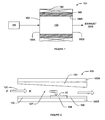
- a deposition system 101 in which embodiments of the present invention may be practiced is schematically shown in plan view in Figure 1 .
- the deposition system 101 may be a horizontal, hot wall, flow through, CVD system as shown including a susceptor assembly 100, a quartz tube 180 defining a through passage 180A, an electromagnetic frequency (EMF) generator 182 (for example, including a power supply and an RF coil surrounding the tube 180) and a process gas supply 160.
- An insulative cover may be provided about the susceptor assembly 100 in addition to or in place of the quartz tube 180.
- the deposition system 101 may be used to form a layer or film on a substrate 20 ( Figure 2 ). While only a single substrate 20 is illustrated in Figure 2 , the system 101 may be adapted to form films concurrently on multiple substrates 20.
- the substrate 20 may be a wafer or other structure formed of the same or a different material than that of the layer to be deposited.
- the substrate 20 may be formed of, for example, SiC, sapphire, a Group III nitride, silicon, germanium, and/or a III-V or II-VI compound or interalloy, or the like.
- the substrate surface upon which the film is deposited may be a base substrate or a first or subsequent layer superimposed on a base substrate.
- the surface of the substrate 20 for receiving the deposited film may be a layer previously deposited using the deposition system 101 or an alternative apparatus.
- embodiments of the present invention may be advantageously utilized with semiconductor materials other than those specifically mentioned herein.
- the process gas supply 160 supplies a process gas into and through the susceptor assembly 100 as discussed below.
- the EMF generator 182 inductively heats the susceptor assembly 100 to provide a hot zone in the susceptor assembly 100 where deposition reactions take place.
- the process gas continues through and out of the susceptor assembly 100 as an exhaust gas that may include remaining components of the process gas as well as reaction by-products, for example.
- Embodiments of the present invention may be used in types of deposition systems other than hot wall CVD systems. Other modifications to the systems and methods of the present invention will be apparent to those of ordinary skill in the art upon reading the description herein.
- the process gas includes one or more components such as reagents, reactants, species, carriers and the like. Where it is desired to form a SiC layer on a substrate, the process gas may include precursor gases such as silane (SiH 4 ) and propane (C 3 H 8 ) along with a carrier gas such as purified hydrogen gas (H 2 ).
- the process gas supply 160 may be provided from one or more pressurized containers of the gases with flow control and/or metering devices as needed.
- FIG. 2 An exemplary conventional susceptor 100 is shown in Figure 2 .
- the susceptor 100 may be used, for example, in a flow through, hot wall, CVD reactor.
- the susceptor 100 has a top susceptor member 100A and a bottom susceptor member 100B.
- the susceptor 100 also has a top liner 103 and a bottom liner 105 defining a reaction chamber 107 therebetween.
- a substrate 20, such as a semiconductor wafer, is positioned in the reaction chamber 107 and may be situated on an interior surface of a platter (which may rotate), for example.
- a process gas P is introduced to the reaction chamber 107 at one end, flowed through the reaction chamber 107 past the substrate 20, and finally exhausted from the reaction chamber 107 at the opposite end.
- the term process gas refers to one or more gases. As indicated by the arrows in the reaction chamber 107 as shown in Figure 2 , as the process gas flows through the reaction chamber 107 a portion of the process gas may contact the substrate 20 as intended and thereby deposit the reagents or reactants on the substrate 20 to form a layer thereon.
- the reaction chamber 107 may have a length of between 0.1 and 1 meter, a width of between 0.05 and 0.5 meter, and a height of between 1 and 10 cm.
- the reaction chamber 107 is not limited to these dimensions, however.
- the susceptor members may include high quality graphite. Examples of CVD deposition systems including improved susceptor designs are found in U.S. Patent Publication No.
- the susceptor members 100A, 100B are formed of a material suitable to generate heat responsive to eddy currents generated therein by the EMF generator 182, such materials and inductive heating arrangements being well known to those of skill in the art.
- the members may be formed of graphite, and more preferably of high purity graphite.
- a platter 154 or the like may be situated between the bottom member 100B and the substrate 20 to support the substrate 20.
- the platter 154 may be rotatively driven by a suitable mechanism (not shown).
- the system may include a gas-driven rotation system as described in Applicant's U.S. Patent 6,569,250 , titled Gas Driven Rotation Apparatus and Method for Forming Silicon Carbide Layers, filed January 8, 2001, and/or as described in Applicant's U.S. Patent 6,797,069 titled Gas Driven Planetary Rotation Apparatus and Methods for Forming Silicon Carbide Layers, filed April 8, 2002.
- the platter 154 may be stationary.
- the platter 154 may be adapted to hold one or multiple substrates 20.
- the platter 154 may be formed of any suitable material such as SiC coated graphite, solid SiC and/or solid SiC alloy.
- the platter 154 may be omitted such that the substrate rests on the bottom member 140, the liner 105, or other suitable support.
- the process gas supply 160 supplies a flow of the process gas P to the reaction chamber 107 through the inlet opening 102.
- the process gas P flows generally in a flow direction R.
- some portion of the process gas and the reagents therein contact the substrate 20 to form the desired layer (e.g., an epilayer) on the exposed surface of the substrate 20.
- the deposition system and process may be a cold wall and/or non-horizontal flow through system and process.
- the deposition system and process may be a vapor phase epitaxy (VPE), liquid phase epitaxy (LPE), or plasma enhanced CVD (PECVD) deposition system and process rather than a CVD system or process.
- VPE vapor phase epitaxy
- LPE liquid phase epitaxy
- PECVD plasma enhanced CVD
- FIG. 3 is an optical image showing a carrot defect in a silicon carbide epitaxial layer. The defect appears as a carrot-shaped ridge in the surface of the material. Although the precise mechanism is unknown, it is presently believed that most, if not all, carrot defects form at the interface between the substrate and the epitaxial layers and then propagate through epitaxial growth.
- Okada et al. report that carrot defects are characterized by several sets of stacking faults on the (0001) plane at their termination, and observed partial dislocations bounding the stacking faults.
- carrot defects tend to form at or near regions in which a high density of threading dislocations is present, such as may be present at the interface between a crystal substrate and an epitaxial layer.
- Carrot defects appear to propagate as stacking faults in prismatic planes which grow in stepwise fashion in the direction of the crystal off-cut. Viewed from the side, the defects appear as triangular stacking faults having a vertex at the substrate/epitaxy interface and an opposite side on the growth surface.
- carrot defects A1 and B1 are present in the epitaxial layer 20.
- epitaxial growth of layer 20 is initiated at time to and terminated at time t 2 .
- Carrot defect A1 nucleates at point X at the interface 12 and propagates upward as the epitaxial layer 20 grows.
- carrot defect A1 is bounded on one side by a threading dislocation 31 in the ⁇ 0001> direction and by a basal plane dislocation 32 aligned in the ⁇ 11 2 0> direction.
- the carrot defect extends along the surface of the epitaxial layer 20 from point Y to point Z.
- the corresponding endpoints Y and Z are labeled on the defect shown in Figure 3 .
- the length of the surface feature of the carrot defect is related to the thickness of the epitaxial layer and the off-axis angle ⁇ illustrated in Figure 11 .
- the length of a carrot defect in the growth plane is inversely proportional to the tangent of the off-axis angle ⁇ .
- the density of carrot defects in an epitaxial layer of silicon carbide may be reduced by arresting the propagation of such defects during epitaxial growth.
- propagation of carrot defects may be arrested by halting and/or reducing the flow of silicon and carbon source gases during normal epitaxial growth, etching a predetermined thickness of the grown epitaxial layer and resuming the flow of silicon and carbon source gases to resume growth of the epitaxial layer to the desired ultimate thickness.
- the process of etching and growing silicon carbide may be performed once or may be repeated multiple times.
- the process according to embodiments of the present invention may be carried out in-situ within the epitaxial deposition chamber. This result may have multiple benefits: the process may be carried out without removing the substrate from the growth chamber, which may be time consuming and potentially exposes the substrate to contamination; the process may be carried out without requiring additional equipment or facilities; and the process can be carried out without significantly reducing material throughput. Furthermore, in particular embodiments of the present invention, the first and second growth processes are carried out without an intervening growth process.
- the scope of the invention includes both in-situ and ex-situ etching of the epitaxial layer.
- propagation of carrot defects is arrested within a highly doped buffer layer of the epitaxial structure, so that the carrot defects do not extend into more lightly doped layers that may, for example, form the active region of resulting devices.
- the effect of carrot defects on device performance can be reduced or minimized.
- any deleterious effects of halting and restarting epitaxial growth may be reduced, minimized or even eliminated.
- the ensuing epitaxial layers that are primarily responsible for device performance may have a lower defect density as a result of carrot defect termination.
- silicon carbide epitaxial growth is initiated to grow a highly doped buffer layer of silicon carbide.
- growth of a silicon carbide epitaxial layer doped with nitrogen, phosphorus, boron and/or aluminum at a concentration of about 1 E 18 cm -3 or greater is initiated by flowing appropriate source gases (e.g. silane, propane and a dopant gas) through a CVD reactor along with a carrier gas.
- source gases e.g. silane, propane and a dopant gas
- a first layer of silicon carbide is grown to a desired thickness.
- the first layer is grown to a thickness of at least about 2.5 microns, however, the first layer may be grown thicker or thinner than 2.5 microns. In a typical embodiment, the first layer is grown to a thickness of about 4 microns.
- the source gases are then turned off or substantially reduced while the carrier gas continues to flow. While the source gases are shut off, the etchant and/or carrier gas etches the first epitaxial layer to reduce the thickness of the first epitaxial layer.
- the etchant gas may include H 2 , HCl, Ar, Cl 2 and/or a carbon-containing gas such as propane.
- the first epitaxial layer may, for example, be etched as much as about 3 microns. The inventors have found that carrot defects may be arrested when the first epitaxial layer is etched by as little as 0.4 microns.
- the flow of source gases is then resumed, and a second epitaxial layer is grown on the first epitaxial layer (or the growth of the first epitaxial layer is resumed).
- the steps of halting the source gases, etching the grown epitaxial layer and restarting the source gases may be repeated multiple times.
- the epitaxial layer may be capped with an additional epitaxial layer that, in some embodiments, includes about 2 microns of silicon carbide.
- the remainder of the epitaxial layers of the structure may then be grown. It has been found that by stopping the flow of source gases, etching the grown silicon carbide layer and growing additional silicon carbide on the etched surface, the majority of carrot defects propagating through the layer are terminated and do not continue to propagate in the subsequently grown layers.
- carrot defect termination is illustrated schematically therein in the case of carrot defect B1 .
- carrot defect B1 originates at the interface 12 between substrate 10 and epitaxial layer 20.
- the flow of source gases is interrupted and growth of epitaxial layer 20 is halted.
- the epitaxial layer 20 then starts to be etched.
- the flow of source gases is resumed at time t 1 , and growth of epitaxial layer 20 continues until time t 2 .
- the interruption of growth and etching of the epitaxial layer 20 causes carrot defect B1 to terminate at interface 22.
- carrot defect B1 is still present in epitaxial layer 20, it may no longer affect the electrical characteristics of devices formed in subsequent epitaxial layers because it is terminated within the epitaxial layer 20. Even though a terminated defect such as carrot defect B1 may still give rise to a morphological feature on the surface of the epitaxial layer, the electrical impact of the defect may be minimized or eliminated.
- not all carrot defects are eliminated by the method of the invention.
- some defects such as carrot defect A1 may continue to propagate through the growth interruption/etch/growth cycle at time t 1 .
- new carrot defects it is possible for new carrot defects to form after the growth interruption.
- significant reduction in the number of carrot defects that propagate to the surface of the epitaxial layer can be obtained.
- Figure 5 is a Nomarski micrograph illustrating carrot defect termination according to aspects of the invention.
- the figure shows the surface of a 40 micron thick epitaxial layer. Two carrot defects are shown in close proximity in Figure 5 .
- the lower carrot ( B2 ) terminated at a growth interruption after 10 microns of growth.
- the upper carrot (A2) propagated through the entire 40 micron layer. Again, even though a morphological feature is visible in connection with carrot defect B2 , the electrically active portion of the defect does not extend to the surface of the layer.
- the endpoints Y, Z of defect A2 and endpoints Y *, Z * of defect B2 are labeled for ease of comparison with defects A1 and B1 in the schematic diagram of Figure 4 .
- defect D1 in Figure 6 new carrot defects may originate at the growth interruption/etch step, as illustrated by defect D1 in Figure 6 .
- the threading dislocation 41 in the ⁇ 0001> may be converted during the interruption/etch step into a basal plane dislocation 43 which propagates in approximately the ⁇ 11 2 0> direction resulting in the shape illustrated.
- FIG. 7(A), 7(B) , 7(C) and 7(D) The defect behavior described above in connection with carrot defects A1 , B1 , C1 and D1 is illustrated in the micrographs of Figures 7(A), 7(B) , 7(C) and 7(D) .
- a layer of silicon carbide was epitaxially grown on a bulk substrate off-cut at an angle of about eight degrees towards the ⁇ 11 2 0> direction. After 10 microns of growth, the flow of source gases was interrupted, and the layers were etched by about one-half micron. Growth of the epitaxial layer was resumed, and the layer was grown an additional 30 microns. The layer was then etched with molten KOH to highlight defects in the material.
- Figures 7(A) -(D) are micrograph images of the etched layers.
- Figure 7(A) illustrates a carrot defect similar to defect A1 that continued to propagate through the growth interruption/etch step.
- the carrot defect extended a distance of 243 microns at the surface of the layer.
- Figure 7(B) illustrates a carrot defect similar to defect B1 that was terminated at the growth interruption/etch step.
- the carrot defect grew to a width of 62 microns before termination. It is noteworthy that the KOH etch did not etch a deep trench where the morphological remnant of the carrot appears, which indicates that the prismatic stacking fault did not propagate to the surface of the epitaxial layer.
- Figure 7(C) illustrates a carrot defect similar to defect C1 that was modified at the growth interruption/etch step such that the threading dislocation in the ⁇ 0001> direction was converted to a dislocation propagating in approximately the ⁇ 11 2 0> direction.
- Figure 7(D) illustrates a carrot defect similar to defect D1 that originated at the growth interruption/etch step.
- the initial epitaxial layer was approximately 5 microns thick, there was a single growth interruption, and the final epitaxial layer was approximately 35 microns thick.
- the initial epitaxial layer was approximately 2.5 microns thick, there was a single growth interruption, and the final epitaxial layer was approximately 37.5 microns thick.
- the initial epitaxial layer was approximately 2.5 microns thick, there were two growth interruptions with an additional 2.5 microns thick epitaxial layer between them, and the final epitaxial layer was approximately 35 microns thick.
- FIG. 8 A histogram of the carrot reduction ratio is presented in Figure 8 .
- the abscissa (x-axis) of Figure 8 represents the ratio of carrot defect densities in wafers prepared using a process according to embodiments of the present invention to wafers that did not use such a process.
- the ordinate (y-axis) represents the percentage of samples falling within the indicated range of defect reduction
- Figure 8 shows that the majority of wafers grown using the inventive process had only 10 to 30% of the number of carrot defects found in the control wafers.
- the median carrot density was reduced from 2.76 cm -2 to 0.67 cm -2 .
- the number of carrots can be reduced by roughly 70-80% of the expected value.
- the present invention may be employed in processes for depositing layers or the like on other types of substrates.
- the systems and methods of the present invention may be particularly useful in processes for forming an epitaxial layer on a substrate.
- heating systems may be used other than or in addition to inductive heating.
- a “system” may include one or multiple elements or features.
- the "deposition system”, the “deposition control system”, the “buffer gas supply system”, the “process gas supply system” and the like are not limited to systems including all of the components, aspects, elements or features discussed above or corresponding components, aspects, elements or features.
Claims (26)
- Verfahren zur Herstellung einer epitaxialen Einkristall-Siliciumcarbid-Schicht auf einem außeraxialen Siliciumcarbid-Substrat, umfassend:das Züchten einer ersten Schicht von epitaxialem Siliciumcarbid auf dem Substrat;das Unterbrechen der Züchtung der ersten Schicht des epitaxialen Siliciumcarbids;anschließend das Ätzen der ersten Schicht des epitaxialen Siliciumcarbids, indem man ein Ätzgas über das Substrat strömen lässt, um die Dicke der ersten Schicht zu verringern; unddas Züchten einer zweiten Schicht von epitaxialem Siliciumcarbid auf der geätzten ersten Schicht von epitaxialem Siliciumcarbid.
- Verfahren nach Anspruch 1, wobei die Züchtung der ersten Schicht von epitaxialem Siliciumcarbid das Strömenlassen von Silicium und Kohlenstoff enthaltenden Quellengasen über das Substrat umfasst und das Unterbrechen des Wachstums der ersten Schicht von epitaxialem Siliciumcarbid die Verringerung des Stroms von Quellengasen umfasst.
- Verfahren nach Anspruch 1, wobei das Züchten der ersten Schicht von epitaxialem Siliciumcarbid das Strömenlassen von Silicium und Kohlenstoff enthaltenden Quellengasen über das Substrat umfasst und das Unterbrechen der Züchtung der ersten Schicht von epitaxialem Siliciumcarbid das Anhalten des Stroms von Quellengasen umfasst.
- Verfahren nach Anspruch 1, wobei das Ätzgas H2, Ar, HCl, Cl2 und/oder Propan umfasst.
- Verfahren nach Anspruch 1, wobei die erste Schicht von epitaxialem Siliciumcarbid mit einem Dotierungsmittel in einer Konzentration von 1E18 cm-3 oder mehr dotiert ist.
- Verfahren nach Anspruch 1, wobei die erste Schicht von epitaxialem Siliciumcarbid eine Dicke von weniger als 4 µm aufweist.
- Verfahren nach Anspruch 1, wobei die erste Schicht von epitaxialem Siliciumcarbid eine Dicke von mehr als 2 µm aufweist.
- Verfahren nach Anspruch 1, wobei die erste Schicht von epitaxialem Siliciumcarbid eine Dicke von 4 µm aufweist.
- Verfahren nach Anspruch 1, wobei das Ätzen der ersten Schicht von epitaxialem Siliciumcarbid das Ätzen der ersten Schicht von epitaxialem Siliciumcarbid um 1 µm oder mehr umfasst.
- Verfahren nach Anspruch 1, wobei das Ätzen der ersten Schicht von epitaxialem Siliciumcarbid das Ätzen der ersten Schicht von epitaxialem Siliciumcarbid um 1 µm oder weniger umfasst.
- Verfahren nach Anspruch 1, wobei die zweite Schicht von epitaxialem Siliciumcarbid bis zu einer Dicke von 2 µm gezüchtet wird.
- Verfahren nach Anspruch 1, ferner umfassend das Ätzen der zweiten epitaxialen Schicht und das Züchten einer dritten epitaxialen Schicht auf der geätzten zweiten epitaxialen Schicht.
- Verfahren nach Anspruch 12, ferner umfassend das Unterbrechen des Wachstums der zweiten epitaxialen Schicht vor dem Ätzen der zweiten epitaxialen Schicht.
- Verfahren nach Anspruch 1, wobei das Substrat Siliciumcarbid mit einem aus 2H, 4H und 6H ausgewählten Polytyp umfasst.
- Verfahren nach Anspruch 1, wobei das Ätzen der ersten Schicht von epitaxialem Siliciumcarbid das Ätzen der ersten Schicht von epitaxialem Siliciumcarbid innerhalb des epitaxialen Züchtungsreaktors erfolgt.
- Verfahren nach Anspruch 1, wobei das Ätzen der ersten Schicht von epitaxialem Siliciumcarbid das Entnehmen des Substrats aus dem epitaxialen Züchtungsreaktor und das Ätzen der ersten Schicht von epitaxialem Siliciumcarbid außerhalb des epitaxialen Züchtungsreaktors umfasst.
- Verfahren nach Anspruch 1, wobei die erste epitaxiale Schicht und die zweite epitaxiale Schicht eine Pufferschicht auf dem Substrat bereitstellen.
- Verfahren nach Anspruch 1, wobei das Züchten der ersten Schicht von epitaxialem Siliciumcarbid auf dem Substrat das Züchten der ersten Schicht von epitaxialem Siliciumcarbid auf einer epitaxialen Schicht auf dem Substrat umfasst.
- Halbleiterstruktur, umfassend eine epitaxiale Siliciumcarbidschicht mit einem Karottendefekt, der innerhalb der epitaxialen Schicht endet und sich nicht bis zur Oberfläche der Schicht erstreckt.
- Halbleiterstruktur nach Anspruch 19, umfassend ein außeraxiales Siliciumcarbid-Substrat, wobei die epitaxiale Schicht von Siliciumcarbid auf dem Substrat gebildet ist und wobei der Karottendefekt einen Nukleisierungspunkt in der Nähe einer Grenzfläche zwischen dem Substrat und der epitaxialen Schicht aufweist.
- Struktur nach Anspruch 20, wobei das Substrat Siliciumcarbid mit einem aus 2H, 4H und 6H ausgewählten Polyptyp umfasst.
- Struktur nach Anspruch 20, wobei das Siliciumcarbid-Substrat außeraxial zur <11
2 0>-Richtung geschnitten ist. - Struktur nach Anspruch 20, wobei das Siliciumcarbid-Substrat außeraxial zu einer kristallographischen Richtung, die senkrecht zur c-Achse steht, geschnitten ist.
- Struktur nach Anspruch 20, wobei die epitaxiale Schicht eine Pufferschicht umfasst.
- Struktur nach Anspruch 20, wobei die epitaxiale Schicht mit einem Dotierungsmittel in einer Konzentration von 1E18 cm-3 oder mehr dotiert ist.
- Struktur nach Anspruch 20, wobei das Dotierungsmittel Stickstoff, Phosphor, Bor oder Aluminium umfasst.
Applications Claiming Priority (2)
| Application Number | Priority Date | Filing Date | Title |
|---|---|---|---|
| US10/790,406 US7230274B2 (en) | 2004-03-01 | 2004-03-01 | Reduction of carrot defects in silicon carbide epitaxy |
| PCT/US2004/038895 WO2005093137A1 (en) | 2004-03-01 | 2004-11-18 | Reduction of carrot defects in silicon carbide epitaxy |
Publications (2)
| Publication Number | Publication Date |
|---|---|
| EP1721031A1 EP1721031A1 (de) | 2006-11-15 |
| EP1721031B1 true EP1721031B1 (de) | 2010-11-17 |
Family
ID=34959915
Family Applications (1)
| Application Number | Title | Priority Date | Filing Date |
|---|---|---|---|
| EP04811590A Active EP1721031B1 (de) | 2004-03-01 | 2004-11-18 | Verringerung von karottendefekten bei der siliciumcarbid-epitaxie |
Country Status (10)
| Country | Link |
|---|---|
| US (2) | US7230274B2 (de) |
| EP (1) | EP1721031B1 (de) |
| JP (1) | JP5268354B2 (de) |
| KR (1) | KR20070008577A (de) |
| CN (1) | CN100472002C (de) |
| AT (1) | ATE488622T1 (de) |
| CA (1) | CA2555431A1 (de) |
| DE (1) | DE602004030161D1 (de) |
| TW (1) | TW200534360A (de) |
| WO (1) | WO2005093137A1 (de) |
Cited By (5)
| Publication number | Priority date | Publication date | Assignee | Title |
|---|---|---|---|---|
| US8860040B2 (en) | 2012-09-11 | 2014-10-14 | Dow Corning Corporation | High voltage power semiconductor devices on SiC |
| US8940614B2 (en) | 2013-03-15 | 2015-01-27 | Dow Corning Corporation | SiC substrate with SiC epitaxial film |
| US9017804B2 (en) | 2013-02-05 | 2015-04-28 | Dow Corning Corporation | Method to reduce dislocations in SiC crystal growth |
| US9018639B2 (en) | 2012-10-26 | 2015-04-28 | Dow Corning Corporation | Flat SiC semiconductor substrate |
| US9279192B2 (en) | 2014-07-29 | 2016-03-08 | Dow Corning Corporation | Method for manufacturing SiC wafer fit for integration with power device manufacturing technology |
Families Citing this family (54)
| Publication number | Priority date | Publication date | Assignee | Title |
|---|---|---|---|---|
| US7173285B2 (en) * | 2004-03-18 | 2007-02-06 | Cree, Inc. | Lithographic methods to reduce stacking fault nucleation sites |
| US20050277302A1 (en) * | 2004-05-28 | 2005-12-15 | Nguyen Son V | Advanced low dielectric constant barrier layers |
| US7682940B2 (en) * | 2004-12-01 | 2010-03-23 | Applied Materials, Inc. | Use of Cl2 and/or HCl during silicon epitaxial film formation |
| US7674337B2 (en) | 2006-04-07 | 2010-03-09 | Applied Materials, Inc. | Gas manifolds for use during epitaxial film formation |
| CN103981568A (zh) * | 2006-07-31 | 2014-08-13 | 应用材料公司 | 形成含碳外延硅层的方法 |
| WO2008033186A1 (en) * | 2006-07-31 | 2008-03-20 | Applied Materials, Inc. | Methods of controlling morphology during epitaxial layer formation |
| JP2008094700A (ja) * | 2006-09-13 | 2008-04-24 | Nippon Steel Corp | 炭化珪素単結晶エピタキシャルウェハ及びその製造方法 |
| JP4844330B2 (ja) * | 2006-10-03 | 2011-12-28 | 富士電機株式会社 | 炭化珪素半導体装置の製造方法および炭化珪素半導体装置 |
| JP4842094B2 (ja) * | 2006-11-02 | 2011-12-21 | 新日本製鐵株式会社 | エピタキシャル炭化珪素単結晶基板の製造方法 |
| US8157914B1 (en) | 2007-02-07 | 2012-04-17 | Chien-Min Sung | Substrate surface modifications for compositional gradation of crystalline materials and associated products |
| US8652255B2 (en) * | 2007-10-12 | 2014-02-18 | The United States Of America, As Represented By The Secretary Of The Navy | Method of producing epitaxial layers with low basal plane dislocation concentrations |
| US8221546B2 (en) | 2008-03-26 | 2012-07-17 | Ss Sc Ip, Llc | Epitaxial growth on low degree off-axis SiC substrates and semiconductor devices made thereby |
| JP5304792B2 (ja) * | 2008-08-29 | 2013-10-02 | 新日鐵住金株式会社 | SiC単結晶膜の製造方法および装置 |
| US8536582B2 (en) * | 2008-12-01 | 2013-09-17 | Cree, Inc. | Stable power devices on low-angle off-cut silicon carbide crystals |
| JP2010184833A (ja) * | 2009-02-12 | 2010-08-26 | Denso Corp | 炭化珪素単結晶基板および炭化珪素単結晶エピタキシャルウェハ |
| US10256090B2 (en) | 2009-08-20 | 2019-04-09 | The United States Of America, As Represented By The Secretary Of The Navy | Reduction of basal plane dislocations in epitaxial SiC using an in-situ etch process |
| US9464366B2 (en) | 2009-08-20 | 2016-10-11 | The United States Of America, As Represented By The Secretary Of The Navy | Reduction of basal plane dislocations in epitaxial SiC |
| US10256094B2 (en) | 2009-08-20 | 2019-04-09 | The Government Of The United States Of America, As Represented By The Secretary Of The Navy | Reduction of basal plane dislocations in epitaxial SiC using an in-situ etch process |
| CN101877309B (zh) * | 2009-10-30 | 2011-09-21 | 西安电子科技大学 | 提高4H-SiC基面位错转化率的外延方法 |
| US8445386B2 (en) * | 2010-05-27 | 2013-05-21 | Cree, Inc. | Smoothing method for semiconductor material and wafers produced by same |
| PL213291B1 (pl) * | 2010-06-07 | 2013-02-28 | Inst Tech Material Elekt | Sposób wytwarzania grafenu |
| CA2779961A1 (en) * | 2010-12-27 | 2012-06-27 | Sumitomo Electric Industries, Ltd. | Silicon carbide substrate, semiconductor device, method of manufacturing silicon carbide substrate and method of manufacturing semiconductor device |
| JP5961357B2 (ja) | 2011-09-09 | 2016-08-02 | 昭和電工株式会社 | SiCエピタキシャルウェハ及びその製造方法 |
| GB201210519D0 (en) | 2012-06-14 | 2012-07-25 | Kromek Ltd | Apparatus and method for crystal growth |
| US20140054609A1 (en) * | 2012-08-26 | 2014-02-27 | Cree, Inc. | Large high-quality epitaxial wafers |
| JP6036200B2 (ja) * | 2012-11-13 | 2016-11-30 | 富士電機株式会社 | 炭化珪素半導体装置の製造方法 |
| US9738991B2 (en) | 2013-02-05 | 2017-08-22 | Dow Corning Corporation | Method for growing a SiC crystal by vapor deposition onto a seed crystal provided on a supporting shelf which permits thermal expansion |
| US9797064B2 (en) | 2013-02-05 | 2017-10-24 | Dow Corning Corporation | Method for growing a SiC crystal by vapor deposition onto a seed crystal provided on a support shelf which permits thermal expansion |
| JP2014154667A (ja) * | 2013-02-07 | 2014-08-25 | Sumitomo Electric Ind Ltd | 半導体装置 |
| JP2014175412A (ja) * | 2013-03-07 | 2014-09-22 | Toshiba Corp | 半導体基板及び半導体装置 |
| WO2014150400A1 (en) * | 2013-03-15 | 2014-09-25 | The Government Of The United States Of America, As Represented By The Secretary Of The Navy | Reduction of basal plane dislocations in epitaxial sic using an in-situ etch process |
| US9919972B2 (en) | 2013-05-02 | 2018-03-20 | Melior Innovations, Inc. | Pressed and self sintered polymer derived SiC materials, applications and devices |
| US11091370B2 (en) | 2013-05-02 | 2021-08-17 | Pallidus, Inc. | Polysilocarb based silicon carbide materials, applications and devices |
| US9657409B2 (en) | 2013-05-02 | 2017-05-23 | Melior Innovations, Inc. | High purity SiOC and SiC, methods compositions and applications |
| US10322936B2 (en) | 2013-05-02 | 2019-06-18 | Pallidus, Inc. | High purity polysilocarb materials, applications and processes |
| CN110747507B (zh) * | 2014-08-01 | 2021-03-19 | 住友电气工业株式会社 | 外延晶片 |
| US9728628B2 (en) * | 2014-08-29 | 2017-08-08 | Sumitomo Electric Industries, Ltd. | Silicon carbide semiconductor device and method for manufacturing same |
| WO2016051975A1 (ja) * | 2014-10-01 | 2016-04-07 | 住友電気工業株式会社 | 炭化珪素エピタキシャル基板 |
| JP6387799B2 (ja) * | 2014-11-14 | 2018-09-12 | 株式会社デンソー | 半導体基板およびその製造方法 |
| JP2016166112A (ja) | 2015-03-10 | 2016-09-15 | 株式会社東芝 | 半導体基板及び半導体装置 |
| CN104851781B (zh) * | 2015-06-08 | 2020-04-14 | 国网智能电网研究院 | 一种n型低偏角碳化硅外延片的制备方法 |
| CN105244255B (zh) * | 2015-08-27 | 2019-03-05 | 中国电子科技集团公司第十三研究所 | 一种碳化硅外延材料及其生产方法 |
| JP2017055086A (ja) * | 2015-09-11 | 2017-03-16 | 昭和電工株式会社 | SiCエピタキシャルウェハの製造方法及びSiCエピタキシャルウェハの製造装置 |
| WO2017061154A1 (ja) * | 2015-10-07 | 2017-04-13 | 住友電気工業株式会社 | 炭化珪素エピタキシャル基板および炭化珪素半導体装置の製造方法 |
| JP6621304B2 (ja) * | 2015-11-10 | 2019-12-18 | 学校法人関西学院 | 半導体ウエハの製造方法 |
| JP6579710B2 (ja) | 2015-12-24 | 2019-09-25 | 昭和電工株式会社 | SiCエピタキシャルウェハの製造方法 |
| JP6965499B2 (ja) * | 2016-03-16 | 2021-11-10 | 富士電機株式会社 | 炭化珪素半導体装置および炭化珪素半導体装置の製造方法 |
| JP6762484B2 (ja) * | 2017-01-10 | 2020-09-30 | 昭和電工株式会社 | SiCエピタキシャルウェハ及びその製造方法 |
| JP7352058B2 (ja) * | 2017-11-01 | 2023-09-28 | セントラル硝子株式会社 | 炭化ケイ素単結晶の製造方法 |
| JP7230551B2 (ja) * | 2019-02-07 | 2023-03-01 | 住友電気工業株式会社 | 炭化珪素エピタキシャル層の厚みの測定方法 |
| TWI723415B (zh) * | 2019-06-05 | 2021-04-01 | 環球晶圓股份有限公司 | 碳化矽晶體及碳化矽晶種片 |
| CN111029246B (zh) * | 2019-12-09 | 2022-07-29 | 中国电子科技集团公司第五十五研究所 | 一种降低SiC外延层中三角形缺陷的方法 |
| CN113745094A (zh) * | 2021-08-31 | 2021-12-03 | 顾赢速科技(合肥)有限公司 | 多层外延工艺制作薄碳化硅晶片圆的方法 |
| CN113654866B (zh) * | 2021-09-22 | 2024-03-01 | 河北光兴半导体技术有限公司 | 一种含有微米级一维铂铑缺陷的薄玻璃样品的制备及缺陷测试方法 |
Family Cites Families (20)
| Publication number | Priority date | Publication date | Assignee | Title |
|---|---|---|---|---|
| US3501356A (en) * | 1966-05-12 | 1970-03-17 | Westinghouse Electric Corp | Process for the epitaxial growth of silicon carbide |
| JPS61151093A (ja) * | 1984-12-25 | 1986-07-09 | Nec Corp | 3−5族化合物半導体の気相エピタキシヤル成長方法 |
| US4659400A (en) * | 1985-06-27 | 1987-04-21 | General Instrument Corp. | Method for forming high yield epitaxial wafers |
| US4912064A (en) * | 1987-10-26 | 1990-03-27 | North Carolina State University | Homoepitaxial growth of alpha-SiC thin films and semiconductor devices fabricated thereon |
| US5248385A (en) * | 1991-06-12 | 1993-09-28 | The United States Of America, As Represented By The Administrator, National Aeronautics And Space Administration | Process for the homoepitaxial growth of single-crystal silicon carbide films on silicon carbide wafers |
| AU2250392A (en) * | 1991-06-12 | 1993-01-12 | Case Western Reserve University | Process for the controlled growth of single-crystal films of silicon carbide polytypes on silicon carbide wafers |
| SE9502288D0 (sv) | 1995-06-26 | 1995-06-26 | Abb Research Ltd | A device and a method for epitaxially growing objects by CVD |
| FR2737734B1 (fr) * | 1995-08-10 | 1997-08-29 | Alcatel Optronics | Procede de gravure d'un substrat par jets chimiques |
| US6063186A (en) * | 1997-12-17 | 2000-05-16 | Cree, Inc. | Growth of very uniform silicon carbide epitaxial layers |
| JP4066528B2 (ja) | 1998-07-31 | 2008-03-26 | 株式会社デンソー | 炭化珪素単結晶の製造方法 |
| JP3443379B2 (ja) * | 1999-03-23 | 2003-09-02 | 松下電器産業株式会社 | 半導体膜の成長方法及び半導体装置の製造方法 |
| JP4457432B2 (ja) * | 1999-06-17 | 2010-04-28 | 株式会社デンソー | 種結晶とそれを用いた炭化珪素単結晶の製造方法、炭化珪素単結晶体および単結晶製造装置 |
| US6329088B1 (en) * | 1999-06-24 | 2001-12-11 | Advanced Technology Materials, Inc. | Silicon carbide epitaxial layers grown on substrates offcut towards <1{overscore (1)}00> |
| JP4742448B2 (ja) * | 2001-06-06 | 2011-08-10 | 株式会社デンソー | 炭化珪素単結晶の製造方法及び製造装置 |
| US6896738B2 (en) | 2001-10-30 | 2005-05-24 | Cree, Inc. | Induction heating devices and methods for controllably heating an article |
| JP4160770B2 (ja) * | 2002-04-04 | 2008-10-08 | 新日本製鐵株式会社 | 4h型炭化珪素単結晶エピタキシャル基板 |
| JP2004043211A (ja) * | 2002-07-09 | 2004-02-12 | Denso Corp | SiC単結晶の製造方法及び製造装置 |
| FR2844095B1 (fr) * | 2002-09-03 | 2005-01-28 | Commissariat Energie Atomique | Procede de fabrication d'un substrat composite du type sicoi comprenant une etape d'epitaxie |
| US6956239B2 (en) * | 2002-11-26 | 2005-10-18 | Cree, Inc. | Transistors having buried p-type layers beneath the source region |
| US7018554B2 (en) | 2003-09-22 | 2006-03-28 | Cree, Inc. | Method to reduce stacking fault nucleation sites and reduce forward voltage drift in bipolar devices |
-
2004
- 2004-03-01 US US10/790,406 patent/US7230274B2/en active Active
- 2004-11-18 DE DE602004030161T patent/DE602004030161D1/de active Active
- 2004-11-18 EP EP04811590A patent/EP1721031B1/de active Active
- 2004-11-18 CN CNB200480042246XA patent/CN100472002C/zh active Active
- 2004-11-18 JP JP2007501768A patent/JP5268354B2/ja active Active
- 2004-11-18 CA CA002555431A patent/CA2555431A1/en not_active Abandoned
- 2004-11-18 WO PCT/US2004/038895 patent/WO2005093137A1/en not_active Application Discontinuation
- 2004-11-18 KR KR1020067017461A patent/KR20070008577A/ko not_active Application Discontinuation
- 2004-11-18 AT AT04811590T patent/ATE488622T1/de not_active IP Right Cessation
-
2005
- 2005-02-25 TW TW094105887A patent/TW200534360A/zh unknown
-
2007
- 2007-05-08 US US11/745,817 patent/US9903046B2/en active Active
Cited By (7)
| Publication number | Priority date | Publication date | Assignee | Title |
|---|---|---|---|---|
| US8860040B2 (en) | 2012-09-11 | 2014-10-14 | Dow Corning Corporation | High voltage power semiconductor devices on SiC |
| US9337277B2 (en) | 2012-09-11 | 2016-05-10 | Dow Corning Corporation | High voltage power semiconductor device on SiC |
| US9018639B2 (en) | 2012-10-26 | 2015-04-28 | Dow Corning Corporation | Flat SiC semiconductor substrate |
| US9017804B2 (en) | 2013-02-05 | 2015-04-28 | Dow Corning Corporation | Method to reduce dislocations in SiC crystal growth |
| US8940614B2 (en) | 2013-03-15 | 2015-01-27 | Dow Corning Corporation | SiC substrate with SiC epitaxial film |
| US9279192B2 (en) | 2014-07-29 | 2016-03-08 | Dow Corning Corporation | Method for manufacturing SiC wafer fit for integration with power device manufacturing technology |
| US10002760B2 (en) | 2014-07-29 | 2018-06-19 | Dow Silicones Corporation | Method for manufacturing SiC wafer fit for integration with power device manufacturing technology |
Also Published As
| Publication number | Publication date |
|---|---|
| CN100472002C (zh) | 2009-03-25 |
| US9903046B2 (en) | 2018-02-27 |
| US20080054412A1 (en) | 2008-03-06 |
| CA2555431A1 (en) | 2005-10-06 |
| US20070108450A1 (en) | 2007-05-17 |
| US7230274B2 (en) | 2007-06-12 |
| TW200534360A (en) | 2005-10-16 |
| WO2005093137A1 (en) | 2005-10-06 |
| JP2007525402A (ja) | 2007-09-06 |
| KR20070008577A (ko) | 2007-01-17 |
| EP1721031A1 (de) | 2006-11-15 |
| CN1926266A (zh) | 2007-03-07 |
| DE602004030161D1 (de) | 2010-12-30 |
| JP5268354B2 (ja) | 2013-08-21 |
| ATE488622T1 (de) | 2010-12-15 |
Similar Documents
| Publication | Publication Date | Title |
|---|---|---|
| EP1721031B1 (de) | Verringerung von karottendefekten bei der siliciumcarbid-epitaxie | |
| Zetterling | Process technology for silicon carbide devices | |
| EP2192211B1 (de) | Vorrichtungen mit stabiler Leistung auf flachwinklig geschnittenen Siliciumcarbidkristallen | |
| EP2059946B1 (de) | Mikroröhrchen-freies siliciumcarbid und verfahren zu seiner herstellung | |
| EP2837020B1 (de) | Herstellungsverfahren eines sic-substrats mit sic epitaxialschicht | |
| EP1786956B1 (de) | Verfahren und anlage mit saathalter zur züchtung von siliziumkarbideinkristalle | |
| US7081420B2 (en) | Method for preparing SiC crystal and SiC crystal | |
| EP1739753A1 (de) | Prozess zur herstellung eines halbleiterbauelements des schottky-sperrschichttyps | |
| JP4603386B2 (ja) | 炭化珪素単結晶の製造方法 | |
| JP4442366B2 (ja) | エピタキシャルSiC膜とその製造方法およびSiC半導体デバイス | |
| JP4408247B2 (ja) | 炭化珪素単結晶育成用種結晶と、それを用いた炭化珪素単結晶の製造方法 | |
| EP1249521B1 (de) | Sic-einkristall und herstellungsverfahren dafür | |
| JP5370025B2 (ja) | 炭化珪素単結晶インゴット | |
| JP2004253751A (ja) | Cvdエピタキシャル成長方法 | |
| Andreev et al. | Influence of growth conditions on the structural perfection of β-SiC epitaxial layers fabricated on 6H-SiC substrates by vacuum sublimation | |
| Schöner | New development in hot wall vapor phase epitaxial growth of silicon carbide | |
| Furukawa et al. | Defect Reduction of Cvd-Grown Cubic SiC Epitaxial Films on Off-Axis Si (100) Substrates with a Novel Off-Direction. | |
| Bhat | Epitaxial Growth of Silicon Carbide by Chemical Vapor Deposition |
Legal Events
| Date | Code | Title | Description |
|---|---|---|---|
| PUAI | Public reference made under article 153(3) epc to a published international application that has entered the european phase |
Free format text: ORIGINAL CODE: 0009012 |
|
| 17P | Request for examination filed |
Effective date: 20060808 |
|
| AK | Designated contracting states |
Kind code of ref document: A1 Designated state(s): AT BE BG CH CY CZ DE DK EE ES FI FR GB GR HU IE IS IT LI LU MC NL PL PT RO SE SI SK TR |
|
| DAX | Request for extension of the european patent (deleted) | ||
| 17Q | First examination report despatched |
Effective date: 20080507 |
|
| GRAP | Despatch of communication of intention to grant a patent |
Free format text: ORIGINAL CODE: EPIDOSNIGR1 |
|
| GRAS | Grant fee paid |
Free format text: ORIGINAL CODE: EPIDOSNIGR3 |
|
| GRAA | (expected) grant |
Free format text: ORIGINAL CODE: 0009210 |
|
| AK | Designated contracting states |
Kind code of ref document: B1 Designated state(s): AT BE BG CH CY CZ DE DK EE ES FI FR GB GR HU IE IS IT LI LU MC NL PL PT RO SE SI SK TR |
|
| REG | Reference to a national code |
Ref country code: GB Ref legal event code: FG4D |
|
| REG | Reference to a national code |
Ref country code: CH Ref legal event code: EP |
|
| REG | Reference to a national code |
Ref country code: IE Ref legal event code: FG4D |
|
| REF | Corresponds to: |
Ref document number: 602004030161 Country of ref document: DE Date of ref document: 20101230 Kind code of ref document: P |
|
| REG | Reference to a national code |
Ref country code: NL Ref legal event code: VDEP Effective date: 20101117 |
|
| PG25 | Lapsed in a contracting state [announced via postgrant information from national office to epo] |
Ref country code: AT Free format text: LAPSE BECAUSE OF FAILURE TO SUBMIT A TRANSLATION OF THE DESCRIPTION OR TO PAY THE FEE WITHIN THE PRESCRIBED TIME-LIMIT Effective date: 20101117 Ref country code: FI Free format text: LAPSE BECAUSE OF FAILURE TO SUBMIT A TRANSLATION OF THE DESCRIPTION OR TO PAY THE FEE WITHIN THE PRESCRIBED TIME-LIMIT Effective date: 20101117 Ref country code: SI Free format text: LAPSE BECAUSE OF FAILURE TO SUBMIT A TRANSLATION OF THE DESCRIPTION OR TO PAY THE FEE WITHIN THE PRESCRIBED TIME-LIMIT Effective date: 20101117 Ref country code: PT Free format text: LAPSE BECAUSE OF FAILURE TO SUBMIT A TRANSLATION OF THE DESCRIPTION OR TO PAY THE FEE WITHIN THE PRESCRIBED TIME-LIMIT Effective date: 20110317 Ref country code: IS Free format text: LAPSE BECAUSE OF FAILURE TO SUBMIT A TRANSLATION OF THE DESCRIPTION OR TO PAY THE FEE WITHIN THE PRESCRIBED TIME-LIMIT Effective date: 20110317 Ref country code: BG Free format text: LAPSE BECAUSE OF FAILURE TO SUBMIT A TRANSLATION OF THE DESCRIPTION OR TO PAY THE FEE WITHIN THE PRESCRIBED TIME-LIMIT Effective date: 20110217 Ref country code: SE Free format text: LAPSE BECAUSE OF FAILURE TO SUBMIT A TRANSLATION OF THE DESCRIPTION OR TO PAY THE FEE WITHIN THE PRESCRIBED TIME-LIMIT Effective date: 20101117 Ref country code: NL Free format text: LAPSE BECAUSE OF FAILURE TO SUBMIT A TRANSLATION OF THE DESCRIPTION OR TO PAY THE FEE WITHIN THE PRESCRIBED TIME-LIMIT Effective date: 20101117 Ref country code: CY Free format text: LAPSE BECAUSE OF FAILURE TO SUBMIT A TRANSLATION OF THE DESCRIPTION OR TO PAY THE FEE WITHIN THE PRESCRIBED TIME-LIMIT Effective date: 20101117 |
|
| PG25 | Lapsed in a contracting state [announced via postgrant information from national office to epo] |
Ref country code: MC Free format text: LAPSE BECAUSE OF NON-PAYMENT OF DUE FEES Effective date: 20101130 Ref country code: GR Free format text: LAPSE BECAUSE OF FAILURE TO SUBMIT A TRANSLATION OF THE DESCRIPTION OR TO PAY THE FEE WITHIN THE PRESCRIBED TIME-LIMIT Effective date: 20110218 |
|
| REG | Reference to a national code |
Ref country code: CH Ref legal event code: PL |
|
| PG25 | Lapsed in a contracting state [announced via postgrant information from national office to epo] |
Ref country code: LI Free format text: LAPSE BECAUSE OF NON-PAYMENT OF DUE FEES Effective date: 20101130 Ref country code: ES Free format text: LAPSE BECAUSE OF FAILURE TO SUBMIT A TRANSLATION OF THE DESCRIPTION OR TO PAY THE FEE WITHIN THE PRESCRIBED TIME-LIMIT Effective date: 20110228 Ref country code: EE Free format text: LAPSE BECAUSE OF FAILURE TO SUBMIT A TRANSLATION OF THE DESCRIPTION OR TO PAY THE FEE WITHIN THE PRESCRIBED TIME-LIMIT Effective date: 20101117 Ref country code: CZ Free format text: LAPSE BECAUSE OF FAILURE TO SUBMIT A TRANSLATION OF THE DESCRIPTION OR TO PAY THE FEE WITHIN THE PRESCRIBED TIME-LIMIT Effective date: 20101117 Ref country code: BE Free format text: LAPSE BECAUSE OF FAILURE TO SUBMIT A TRANSLATION OF THE DESCRIPTION OR TO PAY THE FEE WITHIN THE PRESCRIBED TIME-LIMIT Effective date: 20101117 Ref country code: CH Free format text: LAPSE BECAUSE OF NON-PAYMENT OF DUE FEES Effective date: 20101130 |
|
| PG25 | Lapsed in a contracting state [announced via postgrant information from national office to epo] |
Ref country code: RO Free format text: LAPSE BECAUSE OF FAILURE TO SUBMIT A TRANSLATION OF THE DESCRIPTION OR TO PAY THE FEE WITHIN THE PRESCRIBED TIME-LIMIT Effective date: 20101117 Ref country code: SK Free format text: LAPSE BECAUSE OF FAILURE TO SUBMIT A TRANSLATION OF THE DESCRIPTION OR TO PAY THE FEE WITHIN THE PRESCRIBED TIME-LIMIT Effective date: 20101117 Ref country code: PL Free format text: LAPSE BECAUSE OF FAILURE TO SUBMIT A TRANSLATION OF THE DESCRIPTION OR TO PAY THE FEE WITHIN THE PRESCRIBED TIME-LIMIT Effective date: 20101117 Ref country code: DK Free format text: LAPSE BECAUSE OF FAILURE TO SUBMIT A TRANSLATION OF THE DESCRIPTION OR TO PAY THE FEE WITHIN THE PRESCRIBED TIME-LIMIT Effective date: 20101117 |
|
| PLBE | No opposition filed within time limit |
Free format text: ORIGINAL CODE: 0009261 |
|
| STAA | Information on the status of an ep patent application or granted ep patent |
Free format text: STATUS: NO OPPOSITION FILED WITHIN TIME LIMIT |
|
| 26N | No opposition filed |
Effective date: 20110818 |
|
| PG25 | Lapsed in a contracting state [announced via postgrant information from national office to epo] |
Ref country code: IE Free format text: LAPSE BECAUSE OF NON-PAYMENT OF DUE FEES Effective date: 20101118 |
|
| REG | Reference to a national code |
Ref country code: DE Ref legal event code: R097 Ref document number: 602004030161 Country of ref document: DE Effective date: 20110818 |
|
| PG25 | Lapsed in a contracting state [announced via postgrant information from national office to epo] |
Ref country code: LU Free format text: LAPSE BECAUSE OF NON-PAYMENT OF DUE FEES Effective date: 20101118 Ref country code: HU Free format text: LAPSE BECAUSE OF FAILURE TO SUBMIT A TRANSLATION OF THE DESCRIPTION OR TO PAY THE FEE WITHIN THE PRESCRIBED TIME-LIMIT Effective date: 20110518 |
|
| PG25 | Lapsed in a contracting state [announced via postgrant information from national office to epo] |
Ref country code: TR Free format text: LAPSE BECAUSE OF FAILURE TO SUBMIT A TRANSLATION OF THE DESCRIPTION OR TO PAY THE FEE WITHIN THE PRESCRIBED TIME-LIMIT Effective date: 20101117 |
|
| REG | Reference to a national code |
Ref country code: FR Ref legal event code: PLFP Year of fee payment: 12 |
|
| REG | Reference to a national code |
Ref country code: FR Ref legal event code: PLFP Year of fee payment: 13 |
|
| REG | Reference to a national code |
Ref country code: FR Ref legal event code: PLFP Year of fee payment: 14 |
|
| REG | Reference to a national code |
Ref country code: FR Ref legal event code: PLFP Year of fee payment: 15 |
|
| PGFP | Annual fee paid to national office [announced via postgrant information from national office to epo] |
Ref country code: GB Payment date: 20231127 Year of fee payment: 20 |
|
| PGFP | Annual fee paid to national office [announced via postgrant information from national office to epo] |
Ref country code: IT Payment date: 20231122 Year of fee payment: 20 Ref country code: FR Payment date: 20231127 Year of fee payment: 20 Ref country code: DE Payment date: 20231129 Year of fee payment: 20 |