US7173285B2 - Lithographic methods to reduce stacking fault nucleation sites - Google Patents
Lithographic methods to reduce stacking fault nucleation sites Download PDFInfo
- Publication number
- US7173285B2 US7173285B2 US10/929,226 US92922604A US7173285B2 US 7173285 B2 US7173285 B2 US 7173285B2 US 92922604 A US92922604 A US 92922604A US 7173285 B2 US7173285 B2 US 7173285B2
- Authority
- US
- United States
- Prior art keywords
- silicon carbide
- substrate
- epitaxial
- features
- crystallographic direction
- Prior art date
- Legal status (The legal status is an assumption and is not a legal conclusion. Google has not performed a legal analysis and makes no representation as to the accuracy of the status listed.)
- Active, expires
Links
Images


Classifications
-
- C—CHEMISTRY; METALLURGY
- C30—CRYSTAL GROWTH
- C30B—SINGLE-CRYSTAL GROWTH; UNIDIRECTIONAL SOLIDIFICATION OF EUTECTIC MATERIAL OR UNIDIRECTIONAL DEMIXING OF EUTECTOID MATERIAL; REFINING BY ZONE-MELTING OF MATERIAL; PRODUCTION OF A HOMOGENEOUS POLYCRYSTALLINE MATERIAL WITH DEFINED STRUCTURE; SINGLE CRYSTALS OR HOMOGENEOUS POLYCRYSTALLINE MATERIAL WITH DEFINED STRUCTURE; AFTER-TREATMENT OF SINGLE CRYSTALS OR A HOMOGENEOUS POLYCRYSTALLINE MATERIAL WITH DEFINED STRUCTURE; APPARATUS THEREFOR
- C30B25/00—Single-crystal growth by chemical reaction of reactive gases, e.g. chemical vapour-deposition growth
- C30B25/02—Epitaxial-layer growth
- C30B25/10—Heating of the reaction chamber or the substrate
- C30B25/105—Heating of the reaction chamber or the substrate by irradiation or electric discharge
-
- C—CHEMISTRY; METALLURGY
- C30—CRYSTAL GROWTH
- C30B—SINGLE-CRYSTAL GROWTH; UNIDIRECTIONAL SOLIDIFICATION OF EUTECTIC MATERIAL OR UNIDIRECTIONAL DEMIXING OF EUTECTOID MATERIAL; REFINING BY ZONE-MELTING OF MATERIAL; PRODUCTION OF A HOMOGENEOUS POLYCRYSTALLINE MATERIAL WITH DEFINED STRUCTURE; SINGLE CRYSTALS OR HOMOGENEOUS POLYCRYSTALLINE MATERIAL WITH DEFINED STRUCTURE; AFTER-TREATMENT OF SINGLE CRYSTALS OR A HOMOGENEOUS POLYCRYSTALLINE MATERIAL WITH DEFINED STRUCTURE; APPARATUS THEREFOR
- C30B19/00—Liquid-phase epitaxial-layer growth
- C30B19/12—Liquid-phase epitaxial-layer growth characterised by the substrate
-
- C—CHEMISTRY; METALLURGY
- C30—CRYSTAL GROWTH
- C30B—SINGLE-CRYSTAL GROWTH; UNIDIRECTIONAL SOLIDIFICATION OF EUTECTIC MATERIAL OR UNIDIRECTIONAL DEMIXING OF EUTECTOID MATERIAL; REFINING BY ZONE-MELTING OF MATERIAL; PRODUCTION OF A HOMOGENEOUS POLYCRYSTALLINE MATERIAL WITH DEFINED STRUCTURE; SINGLE CRYSTALS OR HOMOGENEOUS POLYCRYSTALLINE MATERIAL WITH DEFINED STRUCTURE; AFTER-TREATMENT OF SINGLE CRYSTALS OR A HOMOGENEOUS POLYCRYSTALLINE MATERIAL WITH DEFINED STRUCTURE; APPARATUS THEREFOR
- C30B25/00—Single-crystal growth by chemical reaction of reactive gases, e.g. chemical vapour-deposition growth
- C30B25/02—Epitaxial-layer growth
- C30B25/18—Epitaxial-layer growth characterised by the substrate
-
- C—CHEMISTRY; METALLURGY
- C30—CRYSTAL GROWTH
- C30B—SINGLE-CRYSTAL GROWTH; UNIDIRECTIONAL SOLIDIFICATION OF EUTECTIC MATERIAL OR UNIDIRECTIONAL DEMIXING OF EUTECTOID MATERIAL; REFINING BY ZONE-MELTING OF MATERIAL; PRODUCTION OF A HOMOGENEOUS POLYCRYSTALLINE MATERIAL WITH DEFINED STRUCTURE; SINGLE CRYSTALS OR HOMOGENEOUS POLYCRYSTALLINE MATERIAL WITH DEFINED STRUCTURE; AFTER-TREATMENT OF SINGLE CRYSTALS OR A HOMOGENEOUS POLYCRYSTALLINE MATERIAL WITH DEFINED STRUCTURE; APPARATUS THEREFOR
- C30B29/00—Single crystals or homogeneous polycrystalline material with defined structure characterised by the material or by their shape
- C30B29/10—Inorganic compounds or compositions
- C30B29/36—Carbides
-
- H—ELECTRICITY
- H01—ELECTRIC ELEMENTS
- H01L—SEMICONDUCTOR DEVICES NOT COVERED BY CLASS H10
- H01L21/00—Processes or apparatus adapted for the manufacture or treatment of semiconductor or solid state devices or of parts thereof
- H01L21/02—Manufacture or treatment of semiconductor devices or of parts thereof
- H01L21/02104—Forming layers
- H01L21/02365—Forming inorganic semiconducting materials on a substrate
- H01L21/02367—Substrates
- H01L21/0237—Materials
- H01L21/02373—Group 14 semiconducting materials
- H01L21/02378—Silicon carbide
-
- H—ELECTRICITY
- H01—ELECTRIC ELEMENTS
- H01L—SEMICONDUCTOR DEVICES NOT COVERED BY CLASS H10
- H01L21/00—Processes or apparatus adapted for the manufacture or treatment of semiconductor or solid state devices or of parts thereof
- H01L21/02—Manufacture or treatment of semiconductor devices or of parts thereof
- H01L21/02104—Forming layers
- H01L21/02365—Forming inorganic semiconducting materials on a substrate
- H01L21/02367—Substrates
- H01L21/02428—Structure
- H01L21/0243—Surface structure
-
- H—ELECTRICITY
- H01—ELECTRIC ELEMENTS
- H01L—SEMICONDUCTOR DEVICES NOT COVERED BY CLASS H10
- H01L21/00—Processes or apparatus adapted for the manufacture or treatment of semiconductor or solid state devices or of parts thereof
- H01L21/02—Manufacture or treatment of semiconductor devices or of parts thereof
- H01L21/02104—Forming layers
- H01L21/02365—Forming inorganic semiconducting materials on a substrate
- H01L21/02518—Deposited layers
- H01L21/02521—Materials
- H01L21/02524—Group 14 semiconducting materials
- H01L21/02529—Silicon carbide
-
- Y—GENERAL TAGGING OF NEW TECHNOLOGICAL DEVELOPMENTS; GENERAL TAGGING OF CROSS-SECTIONAL TECHNOLOGIES SPANNING OVER SEVERAL SECTIONS OF THE IPC; TECHNICAL SUBJECTS COVERED BY FORMER USPC CROSS-REFERENCE ART COLLECTIONS [XRACs] AND DIGESTS
- Y10—TECHNICAL SUBJECTS COVERED BY FORMER USPC
- Y10S—TECHNICAL SUBJECTS COVERED BY FORMER USPC CROSS-REFERENCE ART COLLECTIONS [XRACs] AND DIGESTS
- Y10S438/00—Semiconductor device manufacturing: process
- Y10S438/931—Silicon carbide semiconductor
Definitions
- This invention relates to semiconductor materials and devices and fabrication methods therefor, and more particularly to methods of growing monocrystalline semiconductor materials, materials formed thereby and devices formed therein.
- the present invention relates to methods of fabricating semiconductor materials used in electronic devices, such as power electronic devices.
- some embodiments of the invention relate to processes that can reduce crystal defects in silicon carbide, and the resulting structures and devices.
- the present invention is related to the subject matter disclosed and claimed in co-pending and commonly assigned application Ser. No. 10/046,346; filed Oct. 26, 2001 and now published as No. 2003-0080842 A1 as well as co-pending and commonly assigned application Ser. No. 10/605,312 filed Sep. 22, 2003; the contents of both of which are incorporated entirely herein by reference in their entirety, as set forth fully herein.
- Silicon carbide has emerged over the last two decades as an appropriate candidate semiconductor material that can offer a number of advantages over both silicon and gallium arsenide.
- silicon carbide has a wide bandgap, a high breakdown electric field, a high thermal conductivity, a high saturated electron drift velocity, and is physically extremely robust.
- Silicon carbide has an extremely high melting point and is one of the hardest known materials in the world.
- silicon carbide Because of its physical properties, however, silicon carbide also may be relatively difficult to produce. Because silicon carbide can grow in many polytypes, it may be difficult to grow into large single crystals. The high temperatures used to grow silicon carbide also may make control of impurity levels (including doping) relatively difficult, and likewise may raise difficulties in the production of thin films (e.g. epitaxial layers). Because of its hardness, the traditional steps of slicing and polishing semiconductor wafers also may be more difficult with silicon carbide. Similarly, its resistance to chemical attack may make it difficult to etch in a conventional fashion.
- silicon carbide can form over 150 polytypes, many of which are separated by relatively small thermodynamic differences.
- epilayers growing single crystal substrates and high quality epitaxial layers (“epilayers”) in silicon carbide has been, and may remain, a difficult task.
- V f forward voltage
- Deposition systems and methods are commonly used to form layers of semiconductor materials, such as thin epitaxial films, on substrates.
- a chemical vapor deposition (CVD) reactor system and process may be used to form a layer of semiconductor material such as silicon carbide (SiC) on a substrate.
- CVD processes may be particularly effective for forming layers with controlled properties, thicknesses, and/or arrangements such as epitaxial layers.
- a deposition system such as a CVD system
- the substrate is placed in a reaction chamber within a susceptor and one or more process gases including reagents or reactants to be deposited on the substrate are introduced into the chamber adjacent the substrate.
- the process gases may be flowed through the reaction chamber in order to provide a uniform or controlled concentration of the reagents or reactants to the substrate.
- a deposition system such as a CVD reactor, may be used to form epitaxial layers of silicon carbide on a single crystal silicon carbide substrate having a predetermined polytype such as 2H, 4H, 6H, 15R, 3C and the like.
- polytype refers to the ordering and arrangement of layers of atoms within a crystal structure.
- the letters H, R and C refer to the general crystal structure of the polytype, namely, hexagonal, rhombohedral and cubic, respectively.
- the numbers in the polytype designations refer to the repetition period of layer arrangements.
- a 4H crystal has a hexagonal crystal structure in which the arrangement of atoms in a crystal repeats every four bi-layers.
- FIG. 1 illustrates a hexagonal unit cell of a hypothetical crystal.
- the unit cell 60 includes a pair of opposing hexagonal faces 61 A, 61 B.
- the hexagonal faces are normal to the c-axis, which runs along the ⁇ 0001> direction as defined by the Miller-Bravais indexing system for designating directions in a hexagonal crystal. Accordingly the hexagonal faces are sometimes called the c-faces, which define the c-planes or basal planes of the crystal. Planes perpendicular to the c-plane are referred to as prismatic planes.
- Silicon carbide possesses a number of potentially advantageous physical and electronic characteristics for semiconductor performance and devices. These may include a wide bandgap, high thermal conductivity, high saturated electron drift velocity, high electron mobility, superior mechanical strength, and radiation hardness.
- the presence of crystalline defects in silicon carbide films may limit the performance of electronic devices fabricated in the films, depending on the type, location, and density of the defects. Accordingly, significant research has focused on reducing defects in silicon carbide films. Certain defects, such as micropipes, are known to severely limit and even prevent device performance. Other defects, such as threading dislocations, are not considered to be individually catastrophic to device operation, and therefore they may not significantly impact device performance at densities normally found in epitaxial films.
- silicon carbide films are usually grown “off-axis.” That is, the substrate crystal is sliced at an angle that is slightly oblique to the normal crystal axis (the c-axis).
- the oblique angle of the cut may be made in one of the standard crystallographic directions illustrated in FIG. 2 , namely the ⁇ 11 2 0> direction (towards a point of the hexagonal unit cell) or the ⁇ 10 1 0> direction (towards the center of a flat side of the hexagonal unit cell), or along a different direction.
- the face of a prepared substrate may be characterized by a periodic arrangement of plateaus and steps. See, for example, U.S. Pat. No. 4,912,064 to Kong et al, entitled Homoepitaxial Growth of Alpha-SiC Thin Films and Semiconductor Devices Fabricated Thereon, assigned to North Carolina State University, the disclosure of which is hereby incorporated herein by reference in its entirety as if set forth fully herein.
- Step-flow growth is illustrated in FIG. 3 .
- Each layer or step grows in the direction in which the crystal was originally cut off-axis (the ⁇ 11 2 0> direction in the case illustrated in FIG. 3 ).
- structural crystallographic defects may fall into four categories: point defects, line defects, planar defects and three dimensional defects.
- Point defects include vacancies
- line defects include dislocations
- planar defects include stacking faults
- three-dimensional defects include polytype inclusions.
- a dislocation is a kind of structural imperfection that extends for many unit cell lengths throughout a crystal. A more definite description of dislocation may classify them as screw and edge dislocations.
- a symmetrical path followed from atom to atom (or from ion to ion) in a real crystal that returns upon itself is referred to as a Burgers circuit. If the same path in the lattice that typifies the structure does not return upon itself, so that the beginning and end do not lie on the same atom, then the Burgers circuit encloses one or more dislocations.
- the vector that completes the closed circuit in the lattice is referred to as the Burgers vector and measures the magnitude and direction of the dislocation.
- the defect is referred to as a screw dislocation.
- the Burgers vector is perpendicular to the dislocation, it is referred to as an edge dislocation.
- the simplest version of an edge dislocation is an incomplete plane of atoms or ions interleaved between two normal planes in a manner somewhat analogous to an extra card inserted halfway into a deck.
- Screw dislocations are not necessarily disadvantageous and, in fact, can be advantageous for the growth of a crystal.
- a 1 C threading screw dislocation at the nominally (0001) oriented growth surface of a silicon carbide crystal presents a regenerating edge that is one or a few atoms high. At this edge, continued growth of the crystal is relatively easy.
- Dislocations allow plastic flow to occur in a crystal relatively easily. Dislocations may move preferentially along slip planes. The dislocation moves relatively easily through the crystal because motion in the slipped plane involves only a slight displacement of the structural elements. Stated differently, the slipped planes provide a low-energy intermediate state by which a crystal can be reorganized.
- SiC wafers and epilayers typically include both screw and edge dislocations. These dislocations can be further grouped by their alignment within the crystal. Those dislocations that propagate along the c-axis are called threading dislocations, while dislocations that lie within the c-plane are termed basal plane dislocations. In general, in SiC, it is energetically favorable that basal plane dislocations may preferentially decompose into partial dislocations via the mechanism described below: 1/3 ⁇ 11 2 0> ⁇ 1/3 ⁇ 10 1 0>+1/3 ⁇ 01 1 0> Equation 1
- the above decomposition reaction describes the decomposition of a basal plane dislocation into two Shockley partial dislocations.
- the line defects generated during the above decomposition will bound a stacking fault defect.
- partial dislocations will generally bind the entire perimeter of the stacking fault unless the stacking fault reaches a free surface.
- This stacking fault will generally be electrically active in bipolar devices, and, during forward operation, the density of the electron-hole plasma may be reduced in the vicinity of the stacking fault. The reduced plasma density may increase the forward voltage of the device.
- a further potential complication is that through recombination enhanced dislocation glide, the stacking fault may continue to expand during forward operation of the device. This behavior can raise a substantial barrier to device exploitation because it can result in devices with functional properties that can change unpredictably during operation.
- the application of electric current through a silicon carbide bipolar device may tend to initiate or propagate (or both) changes in the crystal structure due to preexisting defects in the crystal.
- many SiC polytypes are in close thermodynamic proximity, and solid phase transformations are quite possible.
- the stacking faults impact a significant portion of the active area of a device, they tend to cause the forward voltage to increase in an undesirable manner that can prevent the device from operating as precisely and/or efficiently as required or desired in many applications.
- dislocation density is described by centimeters of dislocation length per cubic centimeter of material, and thus report dislocation density units of per square centimeter (cm ⁇ 2 ).
- dislocation density is described by centimeters of dislocation length per cubic centimeter of material, and thus report dislocation density units of per square centimeter (cm ⁇ 2 ).
- the off-axis orientation of 4H—SiC substrates for SiC epilayer growth and the common etch technique used to detect dislocations make it more convenient to use etch pit density (also in the units of cm ⁇ 2 ), to describe dislocation densities in SiC.
- etch pit density also in the units of cm ⁇ 2
- dislocation density will be described as the density of specific pits delineated on an etched epi-surface of a silicon face prepared, 8° off-axis (0001) oriented substrate.
- 4H—SiC substrates may have approximately 1E3 to 1E5 (about 10 3–10 5 ) dislocations per cm 2 by the convention used herein. This includes threading screw and edge dislocations and basal plane dislocations. Presumably, all types of dislocations can impact device performance, but the basal plane dislocation has been particularly implicated as the prevalent nucleation site of the stacking faults that may cause V f drift.
- SiC-based bipolar and other devices it may be desirable to provide continued improvement in the underlying substrates and their crystal structures.
- Epitaxial silicon carbide layers may be fabricated, according to some embodiments of the present invention, by forming a plurality of features in a surface of a silicon carbide substrate having an off-axis orientation toward a predetermined crystallographic direction.
- the plurality of features includes at least one sidewall that is orientated nonparallel (i.e., oblique or perpendicular) to the predetermined crystallographic direction.
- the epitaxial silicon carbide layer is then grown on the surface of the silicon carbide substrate that includes the plurality of features therein.
- features are formed by masking the surface of the silicon carbide substrate having an off-axis orientation toward a predetermined crystallographic direction and then etching the surface of the silicon carbide substrate that is exposed.
- etching may be performed by dry etching. Dry etching may be performed using an etchant gas etch such as NF 3 and/or SF 6 . In some embodiments, NF 3 is used. In some embodiments the predetermined crystallographic direction is the ⁇ 11 2 0> direction.
- the plurality of features includes a plurality of trenches extending in a direction perpendicular to the predetermined crystallographic direction. In other embodiments, the trenches extend oblique to the predetermined crystallographic direction. Oblique and perpendicular trenches also may be provided. In other embodiments, the plurality of features includes a plurality of pits such as a periodically repeating pattern of hexagonal pits.
- a silicon carbide semiconductor structure includes a silicon carbide substrate having an off-axis orientation toward a predetermined crystallographic direction and including a plurality of features in the surface thereof.
- the plurality of features includes at least one sidewall that is oriented nonparallel (i.e., oblique and/or perpendicular) to the predetermined crystallographic direction.
- An epitaxial silicon carbide layer is also provided on the surface of the silicon carbide substrate that includes the plurality of features therein.
- the predetermined crystallographic direction may be the ⁇ 11 2 0> direction.
- the features may include trenches and/or depressions as was described above.
- inventions of the present invention fabricate an epitaxial silicon carbide layer by epitaxially growing from at least one sidewall of a plurality of features in a surface of the silicon carbide substrate having an off-axis orientation toward a predetermined crystallographic direction to form the epitaxial silicon carbide layer, the at least one sidewall being oriented nonparallel to the predetermined crystallographic direction.
- the features may be trenches and/or depressions as was described above.
- methods and structures according to other embodiments of the present invention may use monocrystalline substrates other than silicon carbide to fabricate one or more epitaxial layers thereon.
- FIG. 1 is a schematic diagram of a hexagonal crystal unit cell structure
- FIG. 2 is a top view of a hexagonal unit cell illustrating standard crystallographic directions
- FIG. 3 is a schematic side view of an off-axis silicon carbide crystal
- FIG. 4 is a schematic view of an epitaxial deposition system
- FIG. 5 is a cross section of a susceptor assembly that can form a part of the deposition system of FIG. 4 ;
- FIG. 6 is a schematic view of a SiC wafer that has been processed in accordance with some embodiments of the invention.
- FIGS. 7A and 7B are magnified views of a portion of the surface of a SiC wafer that has been processed in accordance with some embodiments of the invention.
- FIG. 8A is an interferometry-derived topographic representation of the surface of a silicon carbide wafer that has been patterned in accordance with some embodiments of the invention with a periodic hexagonal pit structure;
- FIG. 8B is a depth profile taken along line B—B of FIG. 8A ;
- FIG. 8C is a depth profile taken along line C—C of FIG. 8A ;
- FIG. 9A is a schematic plan view of the surface of a silicon carbide wafer that has been patterned in accordance with some embodiments of the invention with a periodic trench structure;
- FIG. 9B is a schematic elevation of the structure shown in FIG. 9A ;
- FIG. 9C is a schematic elevation of an alternate embodiment of the structure shown in FIG. 9A ;
- FIG. 10 is a schematic elevation of a structure according to some embodiments of the invention.
- FIG. 11 is a schematic elevation of a structure according to some embodiments of the invention.
- FIG. 12 is a schematic elevation of a structure according to some embodiments of the invention.
- FIG. 13 is a micrograph of the surface of a SiC epitaxial layer according to some embodiments of the invention.
- FIG. 14 is a micrograph of the surface of a SiC epitaxial layer according to further embodiments of the invention.
- FIG. 15 is a micrograph of the surface of a SiC epitaxial layer according to further embodiments of the invention.
- first, second, etc. may be used herein to describe various elements, components, regions, layers and/or sections, these elements, components, regions, layers and/or sections should not be limited by these terms. These terms are only used to distinguish one element, component, region, layer or section from another region, layer or section. Thus, a first element, component, region, layer or section discussed below could be termed a second element, component, region, layer or section without departing from the teachings of the present invention.
- relative terms such as “lower” or “bottom” and “upper” or “top,” may be used herein to describe one element's relationship to another element as illustrated in the Figures. It will be understood that relative terms are intended to encompass different orientations of the device in addition to the orientation depicted in the Figures. For example, if the device in the Figures is turned over, elements described as being on the “lower” side of other elements would then be oriented on “upper” sides of the other elements. The exemplary term “lower”, can therefore, encompass both an orientation of “lower” and “upper,” depending on the particular orientation of the figure.
- Embodiments of the present invention are described herein with reference to cross-sectional and/or other views that are schematic illustrations of idealized embodiments of the present invention. As such, variations from the shapes of the illustrations as a result, for example, of manufacturing techniques and/or tolerances, are to be expected. Thus, embodiments of the present invention should not be construed as limited to the particular shapes of regions illustrated herein but are to include deviations in shapes that result, for example, from manufacturing. For example, a grown or deposited region illustrated as a polygon will, typically, have rounded or curved features and/or a gradient of concentrations at its edges with another region rather than a discrete change from a first region to a second region of different composition. Thus, the regions illustrated in the figures are schematic in nature and their shapes are not intended to illustrate the precise shape of a region of a device and are not intended to limit the scope of the present invention.
- methods of fabricating an epitaxial silicon carbide layer on a silicon carbide substrate having an off-axis orientation toward a first crystallographic direction can include masking the first surface of the substrate with a patterned etch mask, etching the first surface of the substrate to form a plurality of features, each of which includes a sidewall oriented at an angle that is oblique or perpendicular to the first crystallographic direction, and growing an epitaxial layer of silicon carbide on the etched first surface.
- the substrate has an off-axis orientation towards a first crystallographic direction, such as the ⁇ 11 2 0> direction.
- the partially masked substrate may be etched using a dry etch process such as reactive ion etching using NF 3 and/or SF 6 .
- the plurality of features includes a plurality of trenches extending in a direction that is oblique and/or perpendicular to the first crystallographic direction. In other embodiments, the plurality of features includes a periodically repeating pattern of hexagonal depressions.
- a substrate is patterned with a plurality of features including sidewalls and a first epitaxial layer is grown with a first defect density.
- the first epitaxial layer is then patterned with a plurality of features having sidewalls and a second epitaxial layer is grown with a second defect density less than the first defect density.
- Semiconductor structures can include an off-axis silicon carbide substrate having a first surface and an epitaxial layer of silicon carbide formed on the first surface.
- the first surface of the substrate includes a plurality of features, each of which has a sidewall that is perpendicular or oblique to the off-axis crystallographic direction.
- the epitaxial layer has a reduced density of basal plane dislocations compared to the substrate.
- inventions include an off-axis silicon carbide substrate having a first surface and a first epitaxial layer of silicon carbide formed on the first surface.
- the surface of the substrate includes a plurality of features, each of which has a sidewall that is perpendicular or oblique to the off-axis crystallographic direction.
- the first epitaxial layer has a reduced density of basal plane dislocations compared to the substrate.
- the first epitaxial layer further includes a plurality of features, each of which has a sidewall that is perpendicular or oblique to the off-axis crystallographic direction.
- a second epitaxial layer is grown on the first epitaxial layer.
- the second epitaxial layer has a reduced density of basal plane dislocations compared to the first epitaxial layer.
- Some embodiments of the invention can provide methods of reducing stacking fault nucleation site density and/or reducing forward voltage (V f ) drift in silicon carbide-based bipolar devices, and silicon carbide structures having a reduced density of basal plane dislocations that can serve as stacking fault nucleation sites.
- V f forward voltage
- Some embodiments include conducting an etch, such as a dry etch, and in some embodiments a reactive ion etch (RIE) using NF 3 and/or SF 6 chemistry, on a masked surface of a silicon carbide substrate to form a plurality of structures having sidewalls from which epitaxial growth can proceed.
- etch such as a dry etch
- RIE reactive ion etch
- exemplary, but not limiting, techniques for dry etching of silicon carbide are set forth in U.S. Pat. Nos. 4,865,685 and 4,981,551, the contents of which are incorporated entirely herein by reference.
- Other techniques and chemistries for carrying out the etches described herein are generally well-recognized in the art and will not be described in detail herein other than to illustrate embodiments of the invention.
- substrate is used herein in a sense that is broad enough to include both a bulk single crystal (usually cut from a boule) as well as a device precursor structure, such as a wafer, that can include one or more epitaxial layers, but which fundamentally (although not necessarily exclusively) serves as the physical and electronic support for a device formed thereon.
- dry etch and “wet etch,” are often used to refer to reactive ion or plasma etches (“dry”) or to etches in molten salts or other solutions (“wet”).
- the substrate will be n-type, because n-type substrates may offer a number of advantages in silicon carbide-based devices, and may have an activated carrier concentration of about 1E18–1E19 (1 ⁇ 10 18 –1 ⁇ 10 19 ) carriers per cm 3 .
- the carrier concentration of the epitaxial layer may be selected (or described) in terms of its purpose.
- Conductive” layers may typically have a carrier concentration of 1E18–19 cm ⁇ 3 .
- “Blocking” layers may typically have carrier concentrations less than 1E16 cm ⁇ 3 .
- “Active” layers may have carrier concentrations within these parameters, depending on the structure or purpose of the end device. Accordingly, although terms such as n, n+ and n ⁇ can be used to describe both substrates and epilayers, such terminology should be considered in an illustrative rather than a limiting sense.
- the silicon carbide substrate upon which the device is formed can be taken from a larger crystal (or “boule”), typically by the steps of sawing a silicon carbide substrate wafer from a silicon carbide boule, and thereafter conducting a nonselective etch on the substrate wafer.
- the sawed substrate wafer is lapped, polished, etched (typically RIE), and cleaned (with an acid or solvent) prior to conducting a first patterned etch according to some embodiments of the invention.
- lapped is used in its typical sense; i.e., to describe the steps of flattening the wafer surfaces using a counter-rotating lapping machine and an abrasive (e.g. diamond) slurry. Lapping can help make the wafer surfaces parallel and can reduce mechanical defects such as saw markings.
- the polishing, etching and cleaning steps may be otherwise carried out conventionally prior to steps of the present invention.
- Some embodiments of the invention can advantageously reduce the density of basal plane dislocations in the epilayer. This reduction in basal plane dislocation density may be combined with the measures identified to isolate active device regions from the substrate and surface defects discussed in previously-incorporated application Ser. No. 10/046,346, and may be used to provide SiC bipolar devices.
- a deposition system 101 in which some embodiments of the present invention may be practiced is schematically shown in plan view in FIG. 4 .
- the deposition system 101 may be a horizontal, hot wall, flow through, CVD system as shown including a susceptor assembly 100 , a quartz tube 180 defining a through passage 180 A, an electromagnetic frequency (EMF) generator 182 (for example, including a power supply and an RF coil surrounding the tube 180 ) and a process gas supply 160 .
- An insulative cover may be provided about the susceptor assembly 100 in addition to or in place of the quartz tube 180 .
- the deposition system 101 may be used to form a layer or film on a substrate 120 ( FIG. 5 ). While only a single substrate 120 is illustrated in FIG. 5 , the system 101 may be adapted to form films concurrently on multiple substrates 120 .
- the substrate 120 may be a wafer or other structure formed of the same or a different material than that of the layer to be deposited.
- the substrate 120 may be formed of, for example, 2H—, 4H—or 6H—SiC.
- the substrate surface upon which the film is deposited may be a base substrate or a first or subsequent layer superimposed on a base substrate.
- the surface of the substrate 120 for receiving the deposited film may be a layer previously deposited using the deposition system 101 or an alternative apparatus.
- embodiments of the present invention may be advantageously utilized with semiconductor materials other than those specifically mentioned herein.
- the process gas supply 160 supplies a process gas into and through the susceptor assembly 100 as discussed below.
- the EMF generator 182 inductively heats the susceptor assembly 100 to provide a hot zone in the susceptor assembly 100 where deposition reactions take place.
- the process gas continues through and out of the susceptor assembly 100 as an exhaust gas that may include remaining components of the process gas as well as reaction by-products, for example.
- Embodiments of the present invention may use types of deposition systems other than hot wall CVD systems. Other modifications to the systems and methods of the present invention will be apparent to those of ordinary skill in the art upon reading the description herein.
- the process gas may include one or more components such as reagents, reactants, species, carriers and the like. Where it is desired to form a SiC layer on a substrate, the process gas may include precursor gases such as silane (SiH 4 ) and propane (C 3 H 8 ) along with a carrier gas such as purified hydrogen gas (H 2 ).
- the process gas supply 160 may be provided from one or more pressurized containers of the gases with flow control and/or metering devices as needed.
- FIG. 5 An exemplary conventional susceptor 100 is shown in FIG. 5 .
- the susceptor 100 may be used, for example, in a flow through, hot wall, and/or CVD reactor, such as was illustrated in FIG. 4 .
- the susceptor 100 has a top susceptor member 100 A and a bottom susceptor member 100 B.
- the susceptor 100 also has a top liner 103 and a bottom liner 105 defining a reaction chamber 107 therebetween.
- a substrate 120 such as a semiconductor wafer, is positioned in the reaction chamber 107 and may be situated on an interior surface of a platter 154 (which may rotate), for example.
- a process gas P is introduced to the reaction chamber 107 at one end, flowed through the reaction chamber 107 past the substrate 120 , and finally exhausted from the reaction chamber 107 at the opposite end.
- the term process gas refers to one or more gases.
- the reaction chamber 107 may have a length of between about 0.1 and 1 meter, a width of between about 0.05 and 0.5 meter, and a height of between about 1 and 10 cm.
- the reaction chamber 107 is not limited to these dimensions, however.
- the susceptor members may include high quality graphite.
- Examples of CVD deposition systems including susceptor designs are found in U.S. Pat. Publication No. US 2003/0079689 entitled Induction Heating Devices and Methods for Controllably Heating an Article and U.S. patent application Ser. No. 10/414,787, filed Apr. 16, 2003 entitled Methods and Apparatus for Controlling Formation of Deposits in a Deposition System and Depositions Systems and Methods Including the Same both of which are incorporated herein by reference in their entireties.
- the susceptor members 100 A, 100 B are formed of a material suitable to generate heat responsive to eddy currents generated therein by the EMF generator 182 , such materials and inductive heating arrangements being well known to those of skill in the art.
- the members may be formed of graphite, and more preferably of high purity graphite.
- a platter 154 or the like may be situated between the bottom member 100 B and the substrate 120 to support the substrate 120 .
- the platter 154 may be rotatively driven by a suitable mechanism (not shown).
- the system may include a gas-driven rotation system as described in U.S. application Ser. No. 09/756,548, entitled Gas Driven Rotation Apparatus and Method for Forming Silicon Carbide Layers, filed Jan. 8, 2001, and/or as described in U.S. application Ser. No. 10/117,858, entitled Gas Driven Planetary Rotation Apparatus and Methods for Forming Silicon Carbide Layers, filed Apr. 8, 2002, the disclosures of which are hereby incorporated herein by reference in their entireties.
- the platter 154 may be stationary.
- the platter 154 may be adapted to hold one or multiple substrates 120 .
- the platter 154 may be formed of any suitable material such as SiC coated graphite, solid SiC and/or solid SiC alloy.
- the platter 154 may be omitted such that the substrate rests on the susceptor member 100 B, the liner 105 , or other suitable support.
- the process gas supply 160 supplies a flow of the process gas P to the reaction chamber 107 through the inlet opening 102 .
- the process gas P flows generally in a flow direction R.
- some portion of the process gas and the reagents therein contact the substrate 120 to form the desired layer (e.g., an epilayer) on the exposed surface of the substrate 120 .
- the deposition system and process may be a cold wall and/or non-horizontal flow through system and process.
- the deposition system and process may be a vapor phase epitaxy (VPE), liquid phase epitaxy (LPE), or plasma enhanced CVD (PECVD) deposition system and process rather than a CVD system or process.
- VPE vapor phase epitaxy
- LPE liquid phase epitaxy
- PECVD plasma enhanced CVD
- a single crystal silicon carbide substrate wafer 10 on which one or more epitaxial layers is to be grown has a generally circular perimeter.
- a pair of flats has been milled into the wafer to assist in wafer orientation.
- the wafer 10 includes a primary flat 12 and a secondary flat 14 .
- the surface 16 of the wafer corresponds generally to the c-face of the silicon carbide crystal (except that the wafer has been cut at an off-axis angle ⁇ towards the ⁇ 11 2 0> direction.
- the off-axis angle ⁇ may be about 8° in some embodiments.
- the primary flat 12 runs along the ⁇ 11 2 0> direction, while the secondary flat 14 is oriented along the ⁇ 10 1 0> direction.
- the surface 16 of the wafer 10 is masked and etched to form a predefined pattern therein.
- Conventional masks that comprise SiO 2 , Si 3 N 4 , Indium Tin Oxide (ITO) and/or other conventional masking materials may be used.
- the masks may be fabricated and patterned using conventional techniques.
- the etch process may include a reactive ion etch as described above.
- maskless etching and/or selective growth techniques may be used to form the plurality of features in the substrate.
- laser patterning may be used to form the plurality of features in the substrate.
- the pattern includes a plurality of features, which include at least one sidewall oriented at an oblique or perpendicular angle (i.e., nonparallel) to the crystallographic direction in which step-flow epitaxial growth will occur.
- the wafer 10 is cut off-axis towards the ⁇ 11 2 0> direction; thus, epitaxial growth will occur in the ⁇ 11 2 0> direction.
- the wafer includes a plurality of features including at least one sidewall oriented at an oblique or perpendicular angle to the ⁇ 11 2 0> crystallographic direction.
- FIG. 7A is an idealized schematic drawing of a magnified view of a portion 25 of the surface of wafer 10 following etching.
- the surface 16 of the wafer 10 includes a plurality of periodically repeating hexagonal pits 20 etched therein. Each pit is surrounded by six sidewalls 22 .
- at least one pit 20 and in some embodiments each pit 20 , is oriented such that two of its sidewalls run approximately parallel to the crystallographic direction in which epitaxial growth will occur (in this case the ⁇ 11 2 0> direction), while the remaining four sides are oblique to the crystallographic direction in which epitaxial growth will occur.
- At least one pit 20 is oriented such that two of its sidewalls run approximately perpendicular to the crystallographic direction in which epitaxial growth will occur, while the remaining four sides are oblique to the crystallographic direction in which epitaxial growth will occur.
- a hexagonal pit 20 is illustrated in detail in FIG. 7B .
- the pit 20 includes opposing pairs of sidewalls 22 a , 22 b , and 22 c .
- the pit 20 is further characterized by a major axis 24 , which runs through the center of the hexagon between opposing vertices and a minor axis 26 , which runs through the center of the hexagon between opposing sides.
- the hexagonal pits 20 may have a depth of about 0.1 to about 1 ⁇ m and a major axis of about 5 to about 30 ⁇ m. In particular embodiments, the pits 20 may have a depth of about 0.5 ⁇ m and a major axis of about 10 ⁇ m. In some embodiments, the pits 20 may have a ratio of major axis to depth of about 20:1.
- the sidewalls 22 may have a width of about 0.25 to 5 ⁇ m. In particular embodiments, the sidewalls may have a width of about 4 ⁇ m.
- FIGS. 8A–8C illustrate an exemplary structure.
- FIG. 8A is an interferometry-derived topographic representation of the surface of a silicon carbide wafer that has been patterned in accordance with some embodiments of the invention with a periodic hexagonal pit structure.
- FIG. 8B is a depth profile taken along line B—B
- FIG. 8C is a depth profile taken along line C—C.
- the structure illustrated in FIGS. 8A–8C has a major axis of approximately 9.73 ⁇ m, a depth of approximately 0.5 ⁇ m and a sidewall width of approximately 4 ⁇ m.
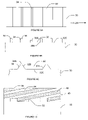
- FIG. 9A illustrates a portion of a substrate 30 on which a series of trenches 32 separated by mesa stripes 34 have been formed, for example, by reactive ion etching.
- the trenches 32 include opposing sidewalls 32 A, 32 B which run perpendicular to the to the crystallographic direction in which step-flow epitaxial growth will occur, in this case the ⁇ 11 2 0> direction.
- the sidewalls are aligned oblique to the crystallographic direction in which step-flow epitaxial growth will occur.
- FIG. 9B is a side view of the substrate 30 showing the trenches 32 and the mesas 34 according to other embodiments.
- the trenches 32 may have a width of about 10 to about 40 ⁇ m.
- the trenches 32 may have a depth of about 0.5 ⁇ m and a width of about 18 ⁇ m.
- the trenches 32 may have a ratio of width to depth of about 36:1.
- the mesas 34 may have a width of about 0.25 to 5 ⁇ m.
- the mesas 34 may have a width of about 3 ⁇ m.
- a mask 36 is also illustrated in the side view of FIG. 9B .
- Sidewalls 32 A, 32 B may be vertical with respect to the floors 32 C of trenches 32 as illustrated in FIG. 9B or they may be angled with respect to floors 32 C as illustrated in FIG. 9C .
- the sidewalls 32 A, 32 B may be straight as illustrated or may comprise curved portions.
- the sidewalls of the feature may be vertical or angled with respect to the substrate and may include straight or curved portions.
- the structure may be etched such that sidewalls 32 A, 32 B are angled with respect to the trench floors 32 C.
- the top portions 34 A of the mesas 34 are narrower than their bases.
- the mesas may have a width of between about 0 and about 5 ⁇ m depending on lithographic and/or other techniques.
- the wafer is placed into an epitaxial growth reactor, such as reactor 100 as described above, and one or more epitaxial layers of silicon carbide are grown on the wafer.
- epitaxial growth of silicon carbide on an off-axis wafer may proceed in step-flow fashion in the direction of the off-axis cut.
- basal plane dislocations are prevented from propagating into the epitaxial layers as basal plane dislocations, those dislocations may not be susceptible to decomposing into stacking faults bounded by Shockley partial dislocations, which can form electrically active stacking faults.
- Substrate 30 includes a plurality of trenches 32 on the surface thereof.
- An epitaxial layer 40 is grown in step-flow fashion from the surface of the substrate.
- regions 42 which nucleate and grow from the sidewalls 32 A of the trenches 32 can have reduced basal plane defect densities compared with regions 44 which do not nucleate and grow from mesa sidewalls.
- regions 42 may exhibit a reduction in basal plane defect density by a factor of 10.
- the percentage of the epitaxial layer 40 that may benefit from defect reduction may depend on the geometry of the features. In particular the sidewall height, width and/or spacing may impact the percentage.
- substrate 30 includes trenches 32 etched therein.
- a first epitaxial layer 40 is grown thereon which includes regions 42 having a reduced basal plane defect density which alternate with regions 44 that may not have reduced basal plane defect density.
- the substrate is masked and etched a second time to form trenches 52 which have sidewalls 52 A, which in some embodiments span the regions 44 .
- the trenches 52 may have the same dimensions as trenches 42 or at least some of the trenches 52 may have different dimensions than at least some of the trenches 42 .
- Epitaxial layer 50 is then grown thereon.
- the basal plane dislocation density of layer 50 may be reduced with respect to the basal plane dislocation density of layer 40 .
- the trenches 52 are formed directly above the trenches 32 formed in the substrate 30 . As illustrated in FIG.
- FIG. 13 is a photograph of a portion of the surface of a silicon carbide wafer that includes mesas 54 that are offset from the underlying mesas 34 .
- FIG. 14 is a Nomarski micrograph of the surface of an epitaxial layer grown on a hex-etched surface in accordance with embodiments of the invention.
- FIG. 15 is a Nomarski micrograph of the surface of an epitaxial layer grown on a line-etched surface in accordance with embodiments of the invention.
- one or more electronic devices such as bipolar devices
- one or more electronic devices may be fabricated in the first and/or second epitaxial silicon carbide layers using techniques that are well known to those having skill in the art.
- the fabrication of electronic devices, such as bipolar devices, is well known to those having skill in the art and need not be described further herein. These devices are not illustrated in FIGS. 10–12 for sake of clarity. Moreover, it will be understood that three or more repetitions of the feature forming and epitaxial-growing steps may be performed.
- Single crystal silicon carbide wafers of the type that may be used as starting structures herein are commercially available from Cree, Inc. 4600 Silicon Drive, Durham, N.C. 27706.
- the growth of silicon carbide epitaxial layers can be carried out using techniques such as those set forth in U.S. Pas. Nos. 4,912,063; 4,912,064; 5,679,153; and 6,297,522. Dry and electrolytic etching of silicon carbide are described in U.S. Pat. Nos.
- molten potassium hydroxide as an etchant to identify and characterize a semiconductor surface is well-understood, and includes versions expressed as ASTM standards (e.g. ASTM F1404.92). Cutting, mechanical polishing and lapping of substrate wafers are also entirely conventional in this art.
Landscapes
- Chemical & Material Sciences (AREA)
- Engineering & Computer Science (AREA)
- Materials Engineering (AREA)
- Crystallography & Structural Chemistry (AREA)
- Metallurgy (AREA)
- Organic Chemistry (AREA)
- Chemical Kinetics & Catalysis (AREA)
- General Chemical & Material Sciences (AREA)
- Physics & Mathematics (AREA)
- Condensed Matter Physics & Semiconductors (AREA)
- General Physics & Mathematics (AREA)
- Manufacturing & Machinery (AREA)
- Computer Hardware Design (AREA)
- Microelectronics & Electronic Packaging (AREA)
- Power Engineering (AREA)
- Inorganic Chemistry (AREA)
- Crystals, And After-Treatments Of Crystals (AREA)
- Chemical Vapour Deposition (AREA)
- Drying Of Semiconductors (AREA)
Abstract
Description
1/3<11
Claims (16)
Priority Applications (9)
| Application Number | Priority Date | Filing Date | Title |
|---|---|---|---|
| US10/929,226 US7173285B2 (en) | 2004-03-18 | 2004-08-30 | Lithographic methods to reduce stacking fault nucleation sites |
| JP2007503906A JP5140415B2 (en) | 2004-03-18 | 2005-02-14 | Lithographic method for reducing stacking fault nucleation sites and structure with reduced stacking fault nucleation sites |
| PCT/US2005/004473 WO2005093795A1 (en) | 2004-03-18 | 2005-02-14 | Lithographic methods to reduce stacking fault nucleation sites and structures having reduced stacking fault nucleation sites |
| EP05722989.0A EP1726036B1 (en) | 2004-03-18 | 2005-02-14 | Lithographic methods to reduce stacking fault nucleation sites and structures having reduced stacking fault nucleation sites |
| KR1020067019093A KR101284398B1 (en) | 2004-03-18 | 2005-02-14 | Lithographic methods to reduce stacking fault nucleation sites and structures having reduced stacking fault nucleation sites |
| CA002554408A CA2554408A1 (en) | 2004-03-18 | 2005-02-14 | Lithographic methods to reduce stacking fault nucleation sites and structures having reduced stacking fault nucleation sites |
| TW094106823A TW200603211A (en) | 2004-03-18 | 2005-03-07 | Lithographic methods to reduce stacking fault nucleation sites and structures having reduced stacking fault nucleation sites |
| US11/615,600 US7601986B2 (en) | 2004-03-18 | 2006-12-22 | Epitaxial semiconductor structures having reduced stacking fault nucleation sites |
| US11/615,614 US7396410B2 (en) | 2004-03-18 | 2006-12-22 | Featuring forming methods to reduce stacking fault nucleation sites |
Applications Claiming Priority (2)
| Application Number | Priority Date | Filing Date | Title |
|---|---|---|---|
| US55412304P | 2004-03-18 | 2004-03-18 | |
| US10/929,226 US7173285B2 (en) | 2004-03-18 | 2004-08-30 | Lithographic methods to reduce stacking fault nucleation sites |
Related Child Applications (2)
| Application Number | Title | Priority Date | Filing Date |
|---|---|---|---|
| US11/615,614 Division US7396410B2 (en) | 2004-03-18 | 2006-12-22 | Featuring forming methods to reduce stacking fault nucleation sites |
| US11/615,600 Division US7601986B2 (en) | 2004-03-18 | 2006-12-22 | Epitaxial semiconductor structures having reduced stacking fault nucleation sites |
Publications (2)
| Publication Number | Publication Date |
|---|---|
| US20050205871A1 US20050205871A1 (en) | 2005-09-22 |
| US7173285B2 true US7173285B2 (en) | 2007-02-06 |
Family
ID=34960748
Family Applications (3)
| Application Number | Title | Priority Date | Filing Date |
|---|---|---|---|
| US10/929,226 Active 2025-01-18 US7173285B2 (en) | 2004-03-18 | 2004-08-30 | Lithographic methods to reduce stacking fault nucleation sites |
| US11/615,614 Expired - Lifetime US7396410B2 (en) | 2004-03-18 | 2006-12-22 | Featuring forming methods to reduce stacking fault nucleation sites |
| US11/615,600 Active 2025-09-08 US7601986B2 (en) | 2004-03-18 | 2006-12-22 | Epitaxial semiconductor structures having reduced stacking fault nucleation sites |
Family Applications After (2)
| Application Number | Title | Priority Date | Filing Date |
|---|---|---|---|
| US11/615,614 Expired - Lifetime US7396410B2 (en) | 2004-03-18 | 2006-12-22 | Featuring forming methods to reduce stacking fault nucleation sites |
| US11/615,600 Active 2025-09-08 US7601986B2 (en) | 2004-03-18 | 2006-12-22 | Epitaxial semiconductor structures having reduced stacking fault nucleation sites |
Country Status (7)
| Country | Link |
|---|---|
| US (3) | US7173285B2 (en) |
| EP (1) | EP1726036B1 (en) |
| JP (1) | JP5140415B2 (en) |
| KR (1) | KR101284398B1 (en) |
| CA (1) | CA2554408A1 (en) |
| TW (1) | TW200603211A (en) |
| WO (1) | WO2005093795A1 (en) |
Cited By (2)
| Publication number | Priority date | Publication date | Assignee | Title |
|---|---|---|---|---|
| US9674678B2 (en) * | 1999-04-21 | 2017-06-06 | Commscope Technologies Llc | Architecture for signal and power distribution in wireless data network |
| US11309389B2 (en) * | 2012-11-30 | 2022-04-19 | Lx Semicon Co., Ltd. | Epitaxial wafer and switch element and light-emitting element using same |
Families Citing this family (14)
| Publication number | Priority date | Publication date | Assignee | Title |
|---|---|---|---|---|
| DE10234976B4 (en) * | 2002-07-31 | 2012-05-03 | Osram Opto Semiconductors Gmbh | Surface emitting semiconductor laser chip and method for its production |
| US7304334B2 (en) | 2005-09-16 | 2007-12-04 | Cree, Inc. | Silicon carbide bipolar junction transistors having epitaxial base regions and multilayer emitters and methods of fabricating the same |
| JP4609335B2 (en) * | 2006-02-02 | 2011-01-12 | 富士電機システムズ株式会社 | Dry etching method for silicon carbide semiconductor substrate |
| US20090085055A1 (en) * | 2007-09-27 | 2009-04-02 | Hui Peng | Method for Growing an Epitaxial Layer |
| JP5392104B2 (en) * | 2010-01-15 | 2014-01-22 | 住友電気工業株式会社 | Light emitting device |
| JP5669134B2 (en) * | 2011-01-21 | 2015-02-12 | 一般財団法人電力中央研究所 | Method for producing silicon carbide single crystal |
| JP5958949B2 (en) * | 2011-05-26 | 2016-08-02 | 一般財団法人電力中央研究所 | Silicon carbide substrate, silicon carbide wafer, silicon carbide wafer manufacturing method, and silicon carbide semiconductor element |
| JP2013089741A (en) * | 2011-10-18 | 2013-05-13 | Renesas Electronics Corp | Semiconductor device, semiconductor substrate, semiconductor device manufacturing method, and semiconductor substrate manufacturing method |
| JP2012199573A (en) * | 2012-06-01 | 2012-10-18 | Nippon Steel Corp | Silicon carbide single crystal wafer |
| JP5688780B2 (en) * | 2013-05-07 | 2015-03-25 | 学校法人関西学院 | SiC substrate, carbon supply feed substrate, and SiC substrate with carbon nanomaterial |
| JP2015061001A (en) * | 2013-09-20 | 2015-03-30 | 株式会社東芝 | Semiconductor device manufacturing method |
| KR101594171B1 (en) * | 2014-06-16 | 2016-02-16 | (재)한국나노기술원 | method for avoiding crack of epi-film grown on semiconductor substrate and manufacturing method of semiconductor devices thereby |
| WO2016166939A1 (en) | 2015-04-17 | 2016-10-20 | 富士電機株式会社 | Semiconductor manufacturing method and sic substrate |
| WO2020184059A1 (en) * | 2019-03-11 | 2020-09-17 | 日本碍子株式会社 | Sic composite substrate and semiconductor device |
Citations (19)
| Publication number | Priority date | Publication date | Assignee | Title |
|---|---|---|---|---|
| US4865685A (en) | 1987-11-03 | 1989-09-12 | North Carolina State University | Dry etching of silicon carbide |
| US4912063A (en) | 1987-10-26 | 1990-03-27 | North Carolina State University | Growth of beta-sic thin films and semiconductor devices fabricated thereon |
| US4912064A (en) | 1987-10-26 | 1990-03-27 | North Carolina State University | Homoepitaxial growth of alpha-SiC thin films and semiconductor devices fabricated thereon |
| US4981551A (en) | 1987-11-03 | 1991-01-01 | North Carolina State University | Dry etching of silicon carbide |
| US5227034A (en) | 1990-10-19 | 1993-07-13 | Siemens Aktiengesellschaft | Method for electrolytic etching of silicon carbide |
| US5571374A (en) | 1995-10-02 | 1996-11-05 | Motorola | Method of etching silicon carbide |
| US5679153A (en) | 1994-11-30 | 1997-10-21 | Cree Research, Inc. | Method for reducing micropipe formation in the epitaxial growth of silicon carbide and resulting silicon carbide structures |
| US6034001A (en) | 1991-10-16 | 2000-03-07 | Kulite Semiconductor Products, Inc. | Method for etching of silicon carbide semiconductor using selective etching of different conductivity types |
| US6297522B1 (en) | 1997-12-17 | 2001-10-02 | Cree, Inc. | Highly uniform silicon carbide epitaxial layers |
| US6452228B1 (en) | 1998-01-05 | 2002-09-17 | Denso Corporation | Silicon carbide semiconductor device |
| US20030042538A1 (en) | 2001-08-29 | 2003-03-06 | Rajesh Kumar | Silicon carbide power device having protective diode and method for manufacturing silicon carbide power device having protective diode |
| US20030080842A1 (en) | 2001-10-26 | 2003-05-01 | Sumakeris Joseph J. | Minimizing degradation of SiC bipolar semiconductor devices |
| US20030079689A1 (en) | 2001-10-30 | 2003-05-01 | Sumakeris Joseph John | Induction heating devices and methods for controllably heating an article |
| US6569250B2 (en) | 2001-01-08 | 2003-05-27 | Cree, Inc. | Gas-driven rotation apparatus and method for forming silicon carbide layers |
| US20030188687A1 (en) | 2002-04-08 | 2003-10-09 | Paisley Michael James | Gas driven planetary rotation apparatus and methods for forming silicon carbide layers |
| US6649497B2 (en) * | 2000-04-11 | 2003-11-18 | Cree, Inc. | Method of forming vias in silicon carbide and resulting devices and circuits |
| DE10334819A1 (en) | 2002-08-09 | 2004-02-26 | Denso Corp., Kariya | Silicon carbide semiconductor device used in electronics comprises a silicon carbide substrate having an error-aligned surface with a specified outer axial direction |
| US20040183079A1 (en) | 2003-02-14 | 2004-09-23 | Nissan Motor Co., Ltd. | Semiconductor device and manufacturing method thereof |
| US7018554B2 (en) * | 2003-09-22 | 2006-03-28 | Cree, Inc. | Method to reduce stacking fault nucleation sites and reduce forward voltage drift in bipolar devices |
Family Cites Families (14)
| Publication number | Priority date | Publication date | Assignee | Title |
|---|---|---|---|---|
| US4961551A (en) * | 1988-11-18 | 1990-10-09 | Hughes Aircraft Company | Stabilization of a spinning spacecraft of arbitary shape |
| JPH09148556A (en) | 1995-11-24 | 1997-06-06 | Mitsubishi Electric Corp | Semiconductor device and its manufacture |
| US6011279A (en) | 1997-04-30 | 2000-01-04 | Cree Research, Inc. | Silicon carbide field controlled bipolar switch |
| JPH1172606A (en) * | 1997-08-29 | 1999-03-16 | Shimadzu Corp | Pattern etching method for sic |
| US6329088B1 (en) * | 1999-06-24 | 2001-12-11 | Advanced Technology Materials, Inc. | Silicon carbide epitaxial layers grown on substrates offcut towards <1{overscore (1)}00> |
| JP3726584B2 (en) * | 1999-09-16 | 2005-12-14 | セイコーエプソン株式会社 | Power supply circuit and electro-optical device |
| JP3427047B2 (en) * | 1999-09-24 | 2003-07-14 | 三洋電機株式会社 | Nitride-based semiconductor device, method of forming nitride-based semiconductor, and method of manufacturing nitride-based semiconductor device |
| JP2003124189A (en) | 2001-10-10 | 2003-04-25 | Fujitsu Ltd | Method of manufacturing semiconductor device |
| EP1306890A2 (en) | 2001-10-25 | 2003-05-02 | Matsushita Electric Industrial Co., Ltd. | Semiconductor substrate and device comprising SiC and method for fabricating the same |
| US6653006B2 (en) * | 2001-10-29 | 2003-11-25 | Exxonmobil Research And Engineering Company | System for fuel cell reformer start-up |
| JP2003151953A (en) * | 2001-11-15 | 2003-05-23 | Sumitomo Electric Ind Ltd | Etching method |
| KR100526343B1 (en) * | 2003-07-21 | 2005-11-08 | 엘지전자 주식회사 | Method for manufacturing ink that contains phosphor powder |
| US7230274B2 (en) * | 2004-03-01 | 2007-06-12 | Cree, Inc | Reduction of carrot defects in silicon carbide epitaxy |
| US7109521B2 (en) | 2004-03-18 | 2006-09-19 | Cree, Inc. | Silicon carbide semiconductor structures including multiple epitaxial layers having sidewalls |
-
2004
- 2004-08-30 US US10/929,226 patent/US7173285B2/en active Active
-
2005
- 2005-02-14 KR KR1020067019093A patent/KR101284398B1/en active IP Right Grant
- 2005-02-14 JP JP2007503906A patent/JP5140415B2/en active Active
- 2005-02-14 CA CA002554408A patent/CA2554408A1/en not_active Abandoned
- 2005-02-14 WO PCT/US2005/004473 patent/WO2005093795A1/en not_active Application Discontinuation
- 2005-02-14 EP EP05722989.0A patent/EP1726036B1/en active Active
- 2005-03-07 TW TW094106823A patent/TW200603211A/en unknown
-
2006
- 2006-12-22 US US11/615,614 patent/US7396410B2/en not_active Expired - Lifetime
- 2006-12-22 US US11/615,600 patent/US7601986B2/en active Active
Patent Citations (20)
| Publication number | Priority date | Publication date | Assignee | Title |
|---|---|---|---|---|
| US4912063A (en) | 1987-10-26 | 1990-03-27 | North Carolina State University | Growth of beta-sic thin films and semiconductor devices fabricated thereon |
| US4912064A (en) | 1987-10-26 | 1990-03-27 | North Carolina State University | Homoepitaxial growth of alpha-SiC thin films and semiconductor devices fabricated thereon |
| US4865685A (en) | 1987-11-03 | 1989-09-12 | North Carolina State University | Dry etching of silicon carbide |
| US4981551A (en) | 1987-11-03 | 1991-01-01 | North Carolina State University | Dry etching of silicon carbide |
| US5227034A (en) | 1990-10-19 | 1993-07-13 | Siemens Aktiengesellschaft | Method for electrolytic etching of silicon carbide |
| US6034001A (en) | 1991-10-16 | 2000-03-07 | Kulite Semiconductor Products, Inc. | Method for etching of silicon carbide semiconductor using selective etching of different conductivity types |
| US5679153A (en) | 1994-11-30 | 1997-10-21 | Cree Research, Inc. | Method for reducing micropipe formation in the epitaxial growth of silicon carbide and resulting silicon carbide structures |
| US5571374A (en) | 1995-10-02 | 1996-11-05 | Motorola | Method of etching silicon carbide |
| US6297522B1 (en) | 1997-12-17 | 2001-10-02 | Cree, Inc. | Highly uniform silicon carbide epitaxial layers |
| US6452228B1 (en) | 1998-01-05 | 2002-09-17 | Denso Corporation | Silicon carbide semiconductor device |
| US6649497B2 (en) * | 2000-04-11 | 2003-11-18 | Cree, Inc. | Method of forming vias in silicon carbide and resulting devices and circuits |
| US6569250B2 (en) | 2001-01-08 | 2003-05-27 | Cree, Inc. | Gas-driven rotation apparatus and method for forming silicon carbide layers |
| US20030042538A1 (en) | 2001-08-29 | 2003-03-06 | Rajesh Kumar | Silicon carbide power device having protective diode and method for manufacturing silicon carbide power device having protective diode |
| US20030080842A1 (en) | 2001-10-26 | 2003-05-01 | Sumakeris Joseph J. | Minimizing degradation of SiC bipolar semiconductor devices |
| US20030079689A1 (en) | 2001-10-30 | 2003-05-01 | Sumakeris Joseph John | Induction heating devices and methods for controllably heating an article |
| US20030188687A1 (en) | 2002-04-08 | 2003-10-09 | Paisley Michael James | Gas driven planetary rotation apparatus and methods for forming silicon carbide layers |
| DE10334819A1 (en) | 2002-08-09 | 2004-02-26 | Denso Corp., Kariya | Silicon carbide semiconductor device used in electronics comprises a silicon carbide substrate having an error-aligned surface with a specified outer axial direction |
| US6853006B2 (en) | 2002-08-09 | 2005-02-08 | Denso Corporation | Silicon carbide semiconductor device |
| US20040183079A1 (en) | 2003-02-14 | 2004-09-23 | Nissan Motor Co., Ltd. | Semiconductor device and manufacturing method thereof |
| US7018554B2 (en) * | 2003-09-22 | 2006-03-28 | Cree, Inc. | Method to reduce stacking fault nucleation sites and reduce forward voltage drift in bipolar devices |
Non-Patent Citations (8)
| Title |
|---|
| "Notification of Transmittal of The International Search Report and the Written Opinion of the International Searching Authority, or the Declaration", "Written Opinion of the International Searching Authority" and "International Search Report", PCT/US2005/004473, May 10, 2005. |
| "Notification of Transmittal of The International Search Report and the Written Opinion of the International Searching Authority, or the Declaration", "Written Opinion of the International Searching Authority" and "International Search Report", PCT/US2005/004480, Oct. 7, 2005. |
| Nikolaev et al., "SiC liquid-phase epitaxy on patterned substrates", Journal of Crystal Growth, 166:607-611 (1996). |
| Nordell et al., "Equilibrium crystal shapes for 6H AND 4H SiC grown on non-planar substrates", Materials Science and Engineering, B61-62:130-134 (1999). |
| Nordell et al., "Homoepitaxy of 6H and 4H SiC on nonplanar substrates", Appl. Phys. Lett., 72(2):197-199 (1998). |
| Richter et al., "Rapid plasma etching of cubit SiC using NF<SUB>3</SUB>/O<SUB>2 </SUB>gas mixtures", Materials Science and Engineering, B46:160-163 (1997). |
| Sumakeris et al., Methods and Apparatus for Controlling Formation of Deposits in a Deposition System and Deposition Systems and Methods Including the Same, U.S. Appl. No. 10/414,787, filed Apr. 16, 2003. |
| Sumakeris, Method to Reduce Stacking Fault Nucleation Sites and Reduce Forward Voltage Drift in Bipolar Devices, U.S. Appl. No. 10/605,312, filed Sep. 22, 2003. |
Cited By (3)
| Publication number | Priority date | Publication date | Assignee | Title |
|---|---|---|---|---|
| US9674678B2 (en) * | 1999-04-21 | 2017-06-06 | Commscope Technologies Llc | Architecture for signal and power distribution in wireless data network |
| US10142813B2 (en) | 1999-04-21 | 2018-11-27 | Commscope Technologies Llc | Architecture for signal and power distribution in wireless data network |
| US11309389B2 (en) * | 2012-11-30 | 2022-04-19 | Lx Semicon Co., Ltd. | Epitaxial wafer and switch element and light-emitting element using same |
Also Published As
| Publication number | Publication date |
|---|---|
| TW200603211A (en) | 2006-01-16 |
| US20050205871A1 (en) | 2005-09-22 |
| US20070101930A1 (en) | 2007-05-10 |
| KR20060128012A (en) | 2006-12-13 |
| EP1726036B1 (en) | 2018-05-16 |
| CA2554408A1 (en) | 2005-10-06 |
| US7601986B2 (en) | 2009-10-13 |
| WO2005093795A1 (en) | 2005-10-06 |
| US7396410B2 (en) | 2008-07-08 |
| JP5140415B2 (en) | 2013-02-06 |
| KR101284398B1 (en) | 2013-07-09 |
| US20070105349A1 (en) | 2007-05-10 |
| JP2007529900A (en) | 2007-10-25 |
| EP1726036A1 (en) | 2006-11-29 |
Similar Documents
| Publication | Publication Date | Title |
|---|---|---|
| US7109521B2 (en) | Silicon carbide semiconductor structures including multiple epitaxial layers having sidewalls | |
| US7601986B2 (en) | Epitaxial semiconductor structures having reduced stacking fault nucleation sites | |
| US8536582B2 (en) | Stable power devices on low-angle off-cut silicon carbide crystals | |
| US5363800A (en) | Process for the controlled growth of single-crystal films of silicon carbide polytypes on silicon carbide wafers | |
| EP1665343B1 (en) | Method for reducing stacking fault nucleation sites in silicon carbide bipolar components | |
| TWI429797B (en) | Group iii nitride semiconductor crystal substrate and semiconductor device | |
| US20080318359A1 (en) | Method of manufacturing silicon carbide semiconductor substrate | |
| US9988738B2 (en) | Method for manufacturing SiC epitaxial wafer | |
| WO2003027363A1 (en) | Method for growing low-defect single crystal heteroepitaxial films | |
| US6461944B2 (en) | Methods for growth of relatively large step-free SiC crystal surfaces | |
| CN100533663C (en) | Lithographic methods to reduce stacking fault nucleation sites and structures having reduced stacking fault nucleation sites | |
| KR20070017097A (en) | METHOD TO REDUCE STACKING FAULT NUCLEATION SITES AND REDUCE Vf DRIFT IN BIPOLAR DEVICES | |
| Lee | Aluminum nitride epitaxy on (0001) sapphire |
Legal Events
| Date | Code | Title | Description |
|---|---|---|---|
| AS | Assignment |
Owner name: ABB AB INCORPORATED, SWEDEN Free format text: ASSIGNMENT OF ASSIGNORS INTEREST;ASSIGNORS:HALLIN, CHRISTER;LENDENMANN, HEINZ;REEL/FRAME:015425/0439;SIGNING DATES FROM 20040827 TO 20040830 |
|
| AS | Assignment |
Owner name: CREE, INC., NORTH CAROLINA Free format text: ASSIGNMENT OF ASSIGNORS INTEREST;ASSIGNOR:ABB AB INCORPORATED;REEL/FRAME:015591/0180 Effective date: 20040810 |
|
| AS | Assignment |
Owner name: NAVY, SECRETARY OF THE UNITED STATES OF AMERICA, V Free format text: CONFIRMATORY LICENSE;ASSIGNOR:CREE INCORPORATED;REEL/FRAME:018641/0757 Effective date: 20061002 |
|
| STCF | Information on status: patent grant |
Free format text: PATENTED CASE |
|
| FPAY | Fee payment |
Year of fee payment: 4 |
|
| FPAY | Fee payment |
Year of fee payment: 8 |
|
| MAFP | Maintenance fee payment |
Free format text: PAYMENT OF MAINTENANCE FEE, 12TH YEAR, LARGE ENTITY (ORIGINAL EVENT CODE: M1553) Year of fee payment: 12 |
|
| AS | Assignment |
Owner name: U.S. BANK TRUST COMPANY, NATIONAL ASSOCIATION, NORTH CAROLINA Free format text: SECURITY INTEREST;ASSIGNOR:WOLFSPEED, INC.;REEL/FRAME:064185/0755 Effective date: 20230623 |