EP1670001A2 - Verfahren zum Lesen nichtflüchtiger Speicherzellen - Google Patents
Verfahren zum Lesen nichtflüchtiger Speicherzellen Download PDFInfo
- Publication number
- EP1670001A2 EP1670001A2 EP05111880A EP05111880A EP1670001A2 EP 1670001 A2 EP1670001 A2 EP 1670001A2 EP 05111880 A EP05111880 A EP 05111880A EP 05111880 A EP05111880 A EP 05111880A EP 1670001 A2 EP1670001 A2 EP 1670001A2
- Authority
- EP
- European Patent Office
- Prior art keywords
- history
- cells
- read reference
- memory
- reference level
- Prior art date
- Legal status (The legal status is an assumption and is not a legal conclusion. Google has not performed a legal analysis and makes no representation as to the accuracy of the status listed.)
- Withdrawn
Links
- 238000000034 method Methods 0.000 title claims abstract description 40
- 238000009826 distribution Methods 0.000 claims abstract description 33
- 230000006870 function Effects 0.000 claims abstract description 6
- 230000009977 dual effect Effects 0.000 claims description 4
- 230000003213 activating effect Effects 0.000 claims description 3
- 150000004767 nitrides Chemical class 0.000 claims description 3
- 230000000694 effects Effects 0.000 description 4
- 230000007812 deficiency Effects 0.000 description 2
- 230000004048 modification Effects 0.000 description 2
- 238000012986 modification Methods 0.000 description 2
- 230000032683 aging Effects 0.000 description 1
- 230000008859 change Effects 0.000 description 1
- 230000001419 dependent effect Effects 0.000 description 1
- 238000001514 detection method Methods 0.000 description 1
- 230000007613 environmental effect Effects 0.000 description 1
- 230000014759 maintenance of location Effects 0.000 description 1
- 230000008520 organization Effects 0.000 description 1
- 239000003973 paint Substances 0.000 description 1
- 239000007787 solid Substances 0.000 description 1
- 238000006467 substitution reaction Methods 0.000 description 1
Images

Classifications
-
- G—PHYSICS
- G11—INFORMATION STORAGE
- G11C—STATIC STORES
- G11C29/00—Checking stores for correct operation ; Subsequent repair; Testing stores during standby or offline operation
- G11C29/04—Detection or location of defective memory elements, e.g. cell constructio details, timing of test signals
- G11C29/08—Functional testing, e.g. testing during refresh, power-on self testing [POST] or distributed testing
- G11C29/12—Built-in arrangements for testing, e.g. built-in self testing [BIST] or interconnection details
- G11C29/18—Address generation devices; Devices for accessing memories, e.g. details of addressing circuits
- G11C29/26—Accessing multiple arrays
- G11C29/28—Dependent multiple arrays, e.g. multi-bit arrays
-
- G—PHYSICS
- G11—INFORMATION STORAGE
- G11C—STATIC STORES
- G11C16/00—Erasable programmable read-only memories
- G11C16/02—Erasable programmable read-only memories electrically programmable
- G11C16/04—Erasable programmable read-only memories electrically programmable using variable threshold transistors, e.g. FAMOS
- G11C16/0466—Erasable programmable read-only memories electrically programmable using variable threshold transistors, e.g. FAMOS comprising cells with charge storage in an insulating layer, e.g. metal-nitride-oxide-silicon [MNOS], silicon-oxide-nitride-oxide-silicon [SONOS]
- G11C16/0475—Erasable programmable read-only memories electrically programmable using variable threshold transistors, e.g. FAMOS comprising cells with charge storage in an insulating layer, e.g. metal-nitride-oxide-silicon [MNOS], silicon-oxide-nitride-oxide-silicon [SONOS] comprising two or more independent storage sites which store independent data
-
- G—PHYSICS
- G11—INFORMATION STORAGE
- G11C—STATIC STORES
- G11C29/00—Checking stores for correct operation ; Subsequent repair; Testing stores during standby or offline operation
- G11C29/02—Detection or location of defective auxiliary circuits, e.g. defective refresh counters
-
- G—PHYSICS
- G11—INFORMATION STORAGE
- G11C—STATIC STORES
- G11C29/00—Checking stores for correct operation ; Subsequent repair; Testing stores during standby or offline operation
- G11C29/02—Detection or location of defective auxiliary circuits, e.g. defective refresh counters
- G11C29/021—Detection or location of defective auxiliary circuits, e.g. defective refresh counters in voltage or current generators
-
- G—PHYSICS
- G11—INFORMATION STORAGE
- G11C—STATIC STORES
- G11C29/00—Checking stores for correct operation ; Subsequent repair; Testing stores during standby or offline operation
- G11C29/02—Detection or location of defective auxiliary circuits, e.g. defective refresh counters
- G11C29/026—Detection or location of defective auxiliary circuits, e.g. defective refresh counters in sense amplifiers
-
- G—PHYSICS
- G11—INFORMATION STORAGE
- G11C—STATIC STORES
- G11C29/00—Checking stores for correct operation ; Subsequent repair; Testing stores during standby or offline operation
- G11C29/04—Detection or location of defective memory elements, e.g. cell constructio details, timing of test signals
- G11C29/50—Marginal testing, e.g. race, voltage or current testing
- G11C29/50004—Marginal testing, e.g. race, voltage or current testing of threshold voltage
-
- G—PHYSICS
- G11—INFORMATION STORAGE
- G11C—STATIC STORES
- G11C16/00—Erasable programmable read-only memories
- G11C16/02—Erasable programmable read-only memories electrically programmable
- G11C16/04—Erasable programmable read-only memories electrically programmable using variable threshold transistors, e.g. FAMOS
Definitions
- the present invention relates to non-volatile memory cells generally and to methods of reading them in particular.
- Dual bit memory cells are known in the art.
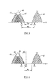
- One such memory cell is the NROM (nitride read only memory) cell 10, shown in Fig. 1 to which reference is now made, which stores two bits 12 and 14 in a nitride based layer 16 sandwiched between a conductive layer 18 and a channel 20.
- NROM cells are described in many patents, for example in U.S Patent No. 6,649,972, assigned to the common assignees of the present invention, whose disclosure is incorporated herein.
- Bits 12 and 14 are individually accessible, and thus, may be programed (conventionally noted as a '0'), erased (conventionally noted as a '1') or read separately. Reading a bit (12 or 14) involves determining if a threshold voltage Vt, as seen when reading the particular bit, is above (programmed) or below (erased) a read reference voltage level RD.
- Fig. 2 illustrates the distribution of programmed and erased states of a memory chip (which typically has a large multiplicity of NROM cells fonned into a memory array) as a function of threshold voltage Vt.
- An erased bit is one whose threshold voltage has been reduced below an erase threshold voltage EV.
- an erase distribution 30 has typically its rightmost point in the vicinity of (and preferably at or below) the erase threshold voltage EV.
- a programmed bit is one whose threshold voltage has been increased above a program threshold voltage PV.
- a programmed distribution 32 has typically its leftmost point in the vicinity of (and preferably at or above) the program threshold voltage PV.
- Read reference voltage level RD is typically placed within window W0 and can be generated, as an example, from a read reference cell.
- the read reference cell is usually, but not necessarily, in a non-native state, as described in US Patent No. 6,490,204, assigned to the common assignee of the present invention, whose disclosure is mcorporated herein by reference.
- the threshold voltage of read reference cell may be at the RD level in Fig. 2.
- the signal from the bit being read is then compared with a comparison circuit (e.g. a differential sense amplifier) to the signal generated by the read reference level, and the result should determine if the anay cell is in a programmed or erased state.
- a comparison circuit e.g. a differential sense amplifier
- the read reference signal can be an independently generated voltage or a current signal. Other methods to generate a read reference signal are known in the art.
- margins M0 and M1 are typically required to correctly read a '0' and a '1', respectively. As long as the programmed and erased distributions are beyond these margins, reliable reads may be achieved.
- Fig. 1 is a schematic illustration of a prior art NROM cell
- Fig. 2 is a schematic illustration of the distribution of programmed and erased states of a memory chip of NROM cells as a function of threshold voltage Vt;
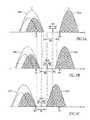
- Fig. 3 is a schematic illustration of erase and programmed distributions at some point after the start of operation of an exemplary memory array
- Fig. 4 is a schematic illustration of erase and programmed distributions once the distributions have shifted from those of Fig. 3;
- Figs. 5A, 5B and 5C are schematic illustrations of a method of reading memory cells, constructed and operative in accordance with the present invention, using a moving read reference level which may move as a function of changes in the window of operation;
- Figs. 6A, 6B and 6C are schematic illustrations of alternative locations of history cells and memory cells, useful in implementing the method of Figs. 5A, 5B and 5C.
- the window of operation may change over time as the cells go tluough multiple erase and programming cycles.
- the window of operation may shrink and/or may drift, both of which may affect the accuracy of the read operation.
- Fig. 3 illustrates erase and programmed distributions 48 and 42, respectively, at some point after the start of operation of an exemplary memory array.
- each bit may be erased to a threshold voltage below erase voltage EV
- erase distribution 40 may appear to be shifted slightly above erase voltage EV Applicants have realized that this may be due to the fact that the two bits of a cell have some effect on each other. If both bits are erased, then the threshold voltage of each bit may be below erase voltage EV (as indicated by the smaller distribution 44 within erase distribution 40). However, if one of the bits is programmed while the other bit is erased, the threshold voltage of the erased bit may appear higher, due to the programmed state of the other bit. This is indicated by the second small distribution 46 within erase distribution 40, some of whose bits may have threshold voltages that appear to be above erase voltage EV. This is typically referred as a "second bit effect".
- programmed distribution 42 may shift below programming voltage PV. This may be due to charge redistribution within the trapping layer, aging characteristics, or retention properties of the cells after many erase/program cycles. This downward shift of the programmed distribution 42 is time and temperature dependent, and the shift rate also depends on the number of program/erase cycles that the cell has experienced in its past.
- Fig. 3 shows an exemplary window Wm with its center shifted from the center of the original window W0. Applicants have realized that one or both of these changes may have an effect on the quality of the read operation. This is illustrated in Fig. 4, to which reference is now made.
- margin M1 may be required to compensate circuit deficiencies and to ensure a correct read of an erased bit.
- the original placement of the erased bits below the EV level (typically after an erase operation), provided a larger than M1 margin, and thus a reliable read of '1' bits.
- margin M1 may no longer be maintained.
- FIG. 5A, 5B and 5C illustrate a method of reading memory cells, constructed and operative in accordance with the present invention, using a moving read reference level MRL, which may move as a function of changes in the window of operation.
- moving read level MRL may be placed at a read level RD1 between an erase distribution 50A and a programmed distribution 52A, where erase distribution 50A is now slightly above erase threshold voltage EV (due to the second bit effect) and programmed distribution 52A is now entirely or almost entirely above programming threshold voltage PV.
- Suitable margins M1 and M0 may be defined from read level RD1 to overcome circuit and sensing scheme deficiencies and to ensure correct detection of the bit states.
- the erase and program distributions are beyond margins M1 and M0, respectively. Therefore, at this paint, read level RD1 may successfully and reliably read both 1's and 0's.
- the distributions may shift.
- the program distribution, now labeled 52B has moved lower and thus, a significant part of it is below program threshold voltage PV.
- the erase distribution, here labeled 50B has typically also moved lower, Even if the window of operation W B is close to or the same width as that in Fig. 5A (labeled W A ), its center has changed. As a result, read reference level RD1 with margin M0 may no longer correctly read all the bits in the program distribution 52B as '0'.
- moving read level MRL may move to a second read level RD2.
- margins M0 and M1 are maintained, but relative to the shifted RD2 read level, and therefore all the bits in both distributions (50B and 52B) may be correctly read as erased ('1') or programmed ('0').
- Fig. 5C shows a third case where the distributions may have shifted further, resulting in a window of operation W C that is further shrunk and/or shifted.
- moving read level MRL may move to a third read level RD3 (along with margins M0 and M1) to accommodate the changed window of operation, and to ensure a reliable read of all the bits in the distributions 50C and 52C.
- read levels RD1 and RD2 would not successfully read the distribution of Fig. 5C. Both read levels RD1 and RD2 would erroneously read at least some of the 0's (since the distance of the left side of the program distribution 52C to the read level is smaller than the required margin M0). Similarly, third read level RD3 would erroneously read some of the 1's had it been used for the distributions of Figs. 5A and 5B since the right sides of distributions 50A and 50B do not maintain a required margin M1 from the read level RD3.
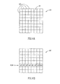
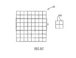
- the memory array may comprise memory cells 62 ta be read, and history cells 64.
- At least one history cell 64 may be associated with a subset of memory cells 62 and may pass through substantially the same events and preferably substantially at the same time and with the same conditions as its corresponding subset of memory cells 62.
- a history cell 64A may be associated with a row A of memory cells 62 and may be programmed and erased at the same time as cells 62 in row A, always being brought back to a its known predetermined state.
- This predetermined, state may be, for example, such that both bits (i.e. both storage areas) of the cell are in a programmed state, or, in a different case, only one of the bits is in a programmed state while the other bit remains erased.
- a set of history cells 64G may be associated with a section G in array 60.
- History cells 64G may be anywhere in the memory array as long as they pass through substantially the same events at substantially the same conditions as the subset of memory cells with whom they are associated.
- the history cells 64G are always brought back to a predetermined state.
- Some of the history cells may have both bits (i.e. both storage areas) in a programmed state while other history cells may have only one of their bits in a programmed state.
- the history cells 64 may be utilized to determine the most appropriate reference read level to use for reading the subset of memory cells 62 to which they are associated.
- the reference read level or more preferably, the highest reference read level, that may produce a correct readout of one history cell 64 (a '0' readout, since the history cells 64 typically are in a programmed state) may be utilized to read its associated subset of memory cells 62.
- the reference read level used to correctly read history cell 64 may be known as a "history read reference level".
- the associated subset of memory cells 62 may be read with a "memory read reference level" which may be the same as the history read reference level or it may have a margin added to it. Alternatively, there may be some other fixed difference between the two read reference levels (YES?).
- RD1>RD2>RD3 there may be three available reference read levels RD1>RD2>RD3. If a programmed history cell 64 is incorrectly read using RD(j) (i.e. it is read as erased), but correctly read using RD(j+1), then the associated subset of memory cells 62 may preferably be read using the RD(j+1) reference read level, with or without a margin added to it.
- a programmed history cell 64 cannot be read with enough margin (Mh) using RD(j) (i.e. it is read as erased using RD(j)+Mh), but can be read with enough margin using RD(j+1) (i.e. it is read as programmed using RD(j+1)+Mh), then the associated subset of memory cells 62 may preferably be read using the RD(j+1) reference read level, with or without margin Mh added to it.
- the margin Mh may be defined as the amount of desired margin between the reliable readout of the history cell and the reliable readout of the memory cells 62 associated therewith.
- the most appropriate reference read level to be used for reading each of the subsets of memory cells 62 may be determined in any one of a number of ways, of which four are described hereinbelow.
- the operations may be performed "on the fly” (before reading the associated subset of memory cells 62) in applications that allow sufficient time to read the history cells 64 vs. the different read reference levels and to determine the optimal memory read reference level for reading the associated subset of memory cells 62.
- the history cells 64 may be read at predetermined times and, after analyzing the readouts and choosing the appropriate read reference level for each set of history cells, the results may be stored for later use when a read of memory cells 62 may be required. Such predetermined times may be at power-up of the device, prior to or after long operations (e.g. program or erase) or at idle times.
- the history cells 64 may be read serially, in parallel, and in a mixed serial/parallel form.
- the history cells 64 may be of the same type of multi bit NROM cells as the array memory cells 62. The may be operated in a one bit per cell mode, in a dual bit per cell mode, or in a multilevel mode. The programmed state of history cells 64 may be achieved by programming only one or both bits in their cells. The history cells 64 may be erased close to, together with, or while erasing their associated memory cells 62. The programming of the history cells may be performed shortly after erasing them and their associated memory cells 62, or close to programming a subset of bits in their associated memory cells 62.
Landscapes
- Engineering & Computer Science (AREA)
- Microelectronics & Electronic Packaging (AREA)
- Read Only Memory (AREA)
Applications Claiming Priority (1)
| Application Number | Priority Date | Filing Date | Title |
|---|---|---|---|
| US11/007,332 US7257025B2 (en) | 2004-12-09 | 2004-12-09 | Method for reading non-volatile memory cells |
Publications (2)
| Publication Number | Publication Date |
|---|---|
| EP1670001A2 true EP1670001A2 (de) | 2006-06-14 |
| EP1670001A3 EP1670001A3 (de) | 2006-09-06 |
Family
ID=36080761
Family Applications (1)
| Application Number | Title | Priority Date | Filing Date |
|---|---|---|---|
| EP05111880A Withdrawn EP1670001A3 (de) | 2004-12-09 | 2005-12-09 | Verfahren zum Lesen nichtflüchtiger Speicherzellen |
Country Status (4)
| Country | Link |
|---|---|
| US (1) | US7257025B2 (de) |
| EP (1) | EP1670001A3 (de) |
| JP (1) | JP2006164507A (de) |
| CN (1) | CN1819055A (de) |
Cited By (1)
| Publication number | Priority date | Publication date | Assignee | Title |
|---|---|---|---|---|
| EP2471069A4 (de) * | 2009-08-25 | 2013-06-12 | Micron Technology Inc | Verfahren, vorrichtungen und systeme zum umgang mit schwellenspannungsänderungen in speichervorrichtungen |
Families Citing this family (45)
| Publication number | Priority date | Publication date | Assignee | Title |
|---|---|---|---|---|
| US6768165B1 (en) | 1997-08-01 | 2004-07-27 | Saifun Semiconductors Ltd. | Two bit non-volatile electrically erasable and programmable semiconductor memory cell utilizing asymmetrical charge trapping |
| US7136304B2 (en) | 2002-10-29 | 2006-11-14 | Saifun Semiconductor Ltd | Method, system and circuit for programming a non-volatile memory array |
| US7178004B2 (en) | 2003-01-31 | 2007-02-13 | Yan Polansky | Memory array programming circuit and a method for using the circuit |
| US7142464B2 (en) | 2003-04-29 | 2006-11-28 | Saifun Semiconductors Ltd. | Apparatus and methods for multi-level sensing in a memory array |
| US7123532B2 (en) | 2003-09-16 | 2006-10-17 | Saifun Semiconductors Ltd. | Operating array cells with matched reference cells |
| US7317633B2 (en) | 2004-07-06 | 2008-01-08 | Saifun Semiconductors Ltd | Protection of NROM devices from charge damage |
| US7095655B2 (en) | 2004-08-12 | 2006-08-22 | Saifun Semiconductors Ltd. | Dynamic matching of signal path and reference path for sensing |
| US7638850B2 (en) | 2004-10-14 | 2009-12-29 | Saifun Semiconductors Ltd. | Non-volatile memory structure and method of fabrication |
| US7535765B2 (en) * | 2004-12-09 | 2009-05-19 | Saifun Semiconductors Ltd. | Non-volatile memory device and method for reading cells |
| EP1684307A1 (de) | 2005-01-19 | 2006-07-26 | Saifun Semiconductors Ltd. | Verfahren, Schaltung und System zum Löschen einer oder mehrerer nichtflüchtiger Speicherzellen |
| EP1746645A3 (de) | 2005-07-18 | 2009-01-21 | Saifun Semiconductors Ltd. | Speicherzellenanordnung mit sub-minimalem Wortleitungsabstand und Verfahren zu deren Herstellung |
| US7668017B2 (en) | 2005-08-17 | 2010-02-23 | Saifun Semiconductors Ltd. | Method of erasing non-volatile memory cells |
| US20070103980A1 (en) * | 2005-11-10 | 2007-05-10 | Gert Koebernick | Method for operating a semiconductor memory device and semiconductor memory device |
| US7808818B2 (en) | 2006-01-12 | 2010-10-05 | Saifun Semiconductors Ltd. | Secondary injection for NROM |
| US8253452B2 (en) | 2006-02-21 | 2012-08-28 | Spansion Israel Ltd | Circuit and method for powering up an integrated circuit and an integrated circuit utilizing same |
| US7760554B2 (en) | 2006-02-21 | 2010-07-20 | Saifun Semiconductors Ltd. | NROM non-volatile memory and mode of operation |
| US7692961B2 (en) | 2006-02-21 | 2010-04-06 | Saifun Semiconductors Ltd. | Method, circuit and device for disturb-control of programming nonvolatile memory cells by hot-hole injection (HHI) and by channel hot-electron (CHE) injection |
| US7638835B2 (en) | 2006-02-28 | 2009-12-29 | Saifun Semiconductors Ltd. | Double density NROM with nitride strips (DDNS) |
| US7701779B2 (en) | 2006-04-27 | 2010-04-20 | Sajfun Semiconductors Ltd. | Method for programming a reference cell |
| WO2008032326A2 (en) * | 2006-09-12 | 2008-03-20 | Saifun Semiconductors Ltd. | Methods, circuits and systems for reading non-volatile memory cells |
| US7605579B2 (en) | 2006-09-18 | 2009-10-20 | Saifun Semiconductors Ltd. | Measuring and controlling current consumption and output current of charge pumps |
| JP5174028B2 (ja) * | 2006-09-27 | 2013-04-03 | サンディスク テクノロジィース インコーポレイテッド | セル集団分布による読み出しマージンを有するメモリ |
| US7716538B2 (en) * | 2006-09-27 | 2010-05-11 | Sandisk Corporation | Memory with cell population distribution assisted read margining |
| US7886204B2 (en) * | 2006-09-27 | 2011-02-08 | Sandisk Corporation | Methods of cell population distribution assisted read margining |
| JP5177991B2 (ja) | 2006-10-25 | 2013-04-10 | 株式会社東芝 | 不揮発性半導体記憶装置 |
| US7864593B2 (en) * | 2007-04-12 | 2011-01-04 | Qimonda Ag | Method for classifying memory cells in an integrated circuit |
| US7876621B2 (en) * | 2007-04-23 | 2011-01-25 | Sandisk Il Ltd. | Adaptive dynamic reading of flash memories |
| KR100888842B1 (ko) * | 2007-06-28 | 2009-03-17 | 삼성전자주식회사 | 읽기 전압을 최적화할 수 있는 플래시 메모리 장치 및그것의 독출 전압 설정 방법 |
| US7675772B2 (en) * | 2007-10-26 | 2010-03-09 | Micron Technology, Inc. | Multilevel memory cell operation |
| US8248855B2 (en) * | 2010-03-10 | 2012-08-21 | Infinite Memories Ltd. | Method of handling reference cells in NVM arrays |
| US8451664B2 (en) | 2010-05-12 | 2013-05-28 | Micron Technology, Inc. | Determining and using soft data in memory devices and systems |
| US8471328B2 (en) | 2010-07-26 | 2013-06-25 | United Microelectronics Corp. | Non-volatile memory and manufacturing method thereof |
| US8687421B2 (en) | 2011-11-21 | 2014-04-01 | Sandisk Technologies Inc. | Scrub techniques for use with dynamic read |
| US9645177B2 (en) * | 2012-05-04 | 2017-05-09 | Seagate Technology Llc | Retention-drift-history-based non-volatile memory read threshold optimization |
| KR102190694B1 (ko) | 2014-03-14 | 2020-12-14 | 삼성전자주식회사 | 불휘발성 메모리 시스템 및 그것의 동작 방법 |
| US9230689B2 (en) | 2014-03-17 | 2016-01-05 | Sandisk Technologies Inc. | Finding read disturbs on non-volatile memories |
| KR102174030B1 (ko) | 2014-05-13 | 2020-11-05 | 삼성전자주식회사 | 불휘발성 메모리 장치를 포함하는 저장 장치 및 그것의 읽기 방법 |
| US9552171B2 (en) | 2014-10-29 | 2017-01-24 | Sandisk Technologies Llc | Read scrub with adaptive counter management |
| US9978456B2 (en) | 2014-11-17 | 2018-05-22 | Sandisk Technologies Llc | Techniques for reducing read disturb in partially written blocks of non-volatile memory |
| US9349479B1 (en) | 2014-11-18 | 2016-05-24 | Sandisk Technologies Inc. | Boundary word line operation in nonvolatile memory |
| US9449700B2 (en) | 2015-02-13 | 2016-09-20 | Sandisk Technologies Llc | Boundary word line search and open block read methods with reduced read disturb |
| US9786386B2 (en) * | 2015-02-27 | 2017-10-10 | Microsoft Technology Licensing, Llc | Dynamic approximate storage for custom applications |
| KR102284658B1 (ko) | 2015-03-19 | 2021-08-02 | 삼성전자 주식회사 | 비휘발성 메모리 장치, 이를 포함하는 메모리 시스템 및 상기 비휘발성 메모리 장치의 동작 방법 |
| US9653154B2 (en) | 2015-09-21 | 2017-05-16 | Sandisk Technologies Llc | Write abort detection for multi-state memories |
| KR20240177463A (ko) | 2023-06-20 | 2024-12-27 | 삼성전자주식회사 | 저장 장치, 및 메모리 컨트롤러의 동작 방법 |
Family Cites Families (107)
| Publication number | Priority date | Publication date | Assignee | Title |
|---|---|---|---|---|
| US4342102A (en) * | 1980-06-18 | 1982-07-27 | Signetics Corporation | Semiconductor memory array |
| US4389705A (en) * | 1981-08-21 | 1983-06-21 | Mostek Corporation | Semiconductor memory circuit with depletion data transfer transistor |
| US4388705A (en) * | 1981-10-01 | 1983-06-14 | Mostek Corporation | Semiconductor memory circuit |
| US5027321A (en) * | 1989-11-21 | 1991-06-25 | Intel Corporation | Apparatus and method for improved reading/programming of virtual ground EPROM arrays |
| EP0461904A3 (en) * | 1990-06-14 | 1992-09-09 | Creative Integrated Systems, Inc. | An improved semiconductor read-only vlsi memory |
| KR920006991A (ko) * | 1990-09-25 | 1992-04-28 | 김광호 | 반도체메모리 장치의 고전압발생회로 |
| JP2987193B2 (ja) * | 1990-11-20 | 1999-12-06 | 富士通株式会社 | 半導体記憶装置 |
| US6002614A (en) * | 1991-02-08 | 1999-12-14 | Btg International Inc. | Memory apparatus including programmable non-volatile multi-bit memory cell, and apparatus and method for demarcating memory states of the cell |
| US5142496A (en) | 1991-06-03 | 1992-08-25 | Advanced Micro Devices, Inc. | Method for measuring VT 's less than zero without applying negative voltages |
| US5245572A (en) * | 1991-07-30 | 1993-09-14 | Intel Corporation | Floating gate nonvolatile memory with reading while writing capability |
| US5142498A (en) * | 1991-08-28 | 1992-08-25 | Exxon Production Research Company | Controlled phase marine source array |
| KR960013022B1 (ko) * | 1991-09-11 | 1996-09-25 | 가와사끼 세이데쯔 가부시끼가이샤 | 반도체 집적회로 |
| JP2564067B2 (ja) * | 1992-01-09 | 1996-12-18 | 株式会社東芝 | センス回路を有する読み出し出力回路 |
| US6222762B1 (en) * | 1992-01-14 | 2001-04-24 | Sandisk Corporation | Multi-state memory |
| US5657332A (en) * | 1992-05-20 | 1997-08-12 | Sandisk Corporation | Soft errors handling in EEPROM devices |
| US5289412A (en) * | 1992-06-19 | 1994-02-22 | Intel Corporation | High-speed bias-stabilized current-mirror referencing circuit for non-volatile memories |
| US5450341A (en) * | 1992-08-31 | 1995-09-12 | Nippon Steel Corporation | Non-volatile semiconductor memory device having memory cells, each for at least three different data writable thereinto selectively and a method of using the same |
| US5450354A (en) * | 1992-08-31 | 1995-09-12 | Nippon Steel Corporation | Non-volatile semiconductor memory device detachable deterioration of memory cells |
| US5412238A (en) * | 1992-09-08 | 1995-05-02 | National Semiconductor Corporation | Source-coupling, split-gate, virtual ground flash EEPROM array |
| US5418743A (en) * | 1992-12-07 | 1995-05-23 | Nippon Steel Corporation | Method of writing into non-volatile semiconductor memory |
| US5335198A (en) * | 1993-05-06 | 1994-08-02 | Advanced Micro Devices, Inc. | Flash EEPROM array with high endurance |
| US5463586A (en) * | 1993-05-28 | 1995-10-31 | Macronix International Co., Ltd. | Erase and program verification circuit for non-volatile memory |
| US5477499A (en) * | 1993-10-13 | 1995-12-19 | Advanced Micro Devices, Inc. | Memory architecture for a three volt flash EEPROM |
| US5828601A (en) * | 1993-12-01 | 1998-10-27 | Advanced Micro Devices, Inc. | Programmed reference |
| JP3076185B2 (ja) | 1993-12-07 | 2000-08-14 | 日本電気株式会社 | 半導体メモリ装置及びその検査方法 |
| EP0678871B1 (de) * | 1994-03-22 | 2000-05-31 | STMicroelectronics S.r.l. | Anordnung zum Lesen einer Speicherzellenmatrix |
| US5568085A (en) * | 1994-05-16 | 1996-10-22 | Waferscale Integration Inc. | Unit for stabilizing voltage on a capacitive node |
| JP3197168B2 (ja) | 1994-10-03 | 2001-08-13 | 松下電器産業株式会社 | 半導体記憶装置の駆動方法 |
| US5508968A (en) * | 1994-08-12 | 1996-04-16 | International Business Machines Corporation | Dynamic random access memory persistent page implemented as processor register sets |
| US5583808A (en) * | 1994-09-16 | 1996-12-10 | National Semiconductor Corporation | EPROM array segmented for high performance and method for controlling same |
| US5694356A (en) * | 1994-11-02 | 1997-12-02 | Invoice Technology, Inc. | High resolution analog storage EPROM and flash EPROM |
| US5537358A (en) * | 1994-12-06 | 1996-07-16 | National Semiconductor Corporation | Flash memory having adaptive sensing and method |
| US5521970A (en) * | 1995-03-29 | 1996-05-28 | At&T Corp. | Arrangement for extending call-coverage across a network of nodes |
| EP0740307B1 (de) | 1995-04-28 | 2001-12-12 | STMicroelectronics S.r.l. | Leseverstärkerschaltung für Halbleiterspeicheranordnungen |
| DE69514790T2 (de) * | 1995-07-14 | 2000-08-03 | Stmicroelectronics S.R.L., Agrate Brianza | Verfahren zur Einstellung der Schwellspannung einer Referenzspeicherzelle |
| US5633603A (en) * | 1995-12-26 | 1997-05-27 | Hyundai Electronics Industries Co., Ltd. | Data output buffer using pass transistors biased with a reference voltage and a precharged data input |
| US5748534A (en) * | 1996-03-26 | 1998-05-05 | Invox Technology | Feedback loop for reading threshold voltage |
| US5777923A (en) * | 1996-06-17 | 1998-07-07 | Aplus Integrated Circuits, Inc. | Flash memory read/write controller |
| US5712815A (en) * | 1996-04-22 | 1998-01-27 | Advanced Micro Devices, Inc. | Multiple bits per-cell flash EEPROM capable of concurrently programming and verifying memory cells and reference cells |
| US5847441A (en) * | 1996-05-10 | 1998-12-08 | Micron Technology, Inc. | Semiconductor junction antifuse circuit |
| US5886927A (en) * | 1996-06-11 | 1999-03-23 | Nkk Corporation | Nonvolatile memory device with verify function |
| WO1997050089A1 (en) * | 1996-06-24 | 1997-12-31 | Advanced Micro Devices, Inc. | A method for a multiple bits-per-cell flash eeprom with page mode program and read |
| KR100265574B1 (ko) * | 1996-06-29 | 2000-09-15 | 김영환 | 반도체 메모리장치의 감지증폭기 |
| US5787484A (en) * | 1996-08-08 | 1998-07-28 | Micron Technology, Inc. | System and method which compares data preread from memory cells to data to be written to the cells |
| US5812456A (en) * | 1996-10-01 | 1998-09-22 | Microchip Technology Incorporated | Switched ground read for EPROM memory array |
| US5717632A (en) | 1996-11-27 | 1998-02-10 | Advanced Micro Devices, Inc. | Apparatus and method for multiple-level storage in non-volatile memories |
| JP3532725B2 (ja) * | 1997-02-27 | 2004-05-31 | 株式会社東芝 | 半導体集積回路 |
| JP3920415B2 (ja) * | 1997-03-31 | 2007-05-30 | 三洋電機株式会社 | 不揮発性半導体メモリ装置 |
| US6252799B1 (en) * | 1997-04-11 | 2001-06-26 | Programmable Silicon Solutions | Device with embedded flash and EEPROM memories |
| US5805500A (en) * | 1997-06-18 | 1998-09-08 | Sgs-Thomson Microelectronics S.R.L. | Circuit and method for generating a read reference signal for nonvolatile memory cells |
| JP3189740B2 (ja) * | 1997-06-20 | 2001-07-16 | 日本電気株式会社 | 不揮発性半導体メモリのデータ修復方法 |
| JP3039458B2 (ja) * | 1997-07-07 | 2000-05-08 | 日本電気株式会社 | 不揮発性半導体メモリ |
| US5940332A (en) * | 1997-11-13 | 1999-08-17 | Stmicroelectronics, Inc. | Programmed memory with improved speed and power consumption |
| US5867429A (en) * | 1997-11-19 | 1999-02-02 | Sandisk Corporation | High density non-volatile flash memory without adverse effects of electric field coupling between adjacent floating gates |
| US5949728A (en) * | 1997-12-12 | 1999-09-07 | Scenix Semiconductor, Inc. | High speed, noise immune, single ended sensing scheme for non-volatile memories |
| US5946258A (en) * | 1998-03-16 | 1999-08-31 | Intel Corporation | Pump supply self regulation for flash memory cell pair reference circuit |
| DE69828966D1 (de) * | 1998-09-15 | 2005-03-17 | St Microelectronics Srl | Verfahren zum Schutz des Inhalts nichtflüchtiger Speicherzellen |
| US6044019A (en) * | 1998-10-23 | 2000-03-28 | Sandisk Corporation | Non-volatile memory with improved sensing and method therefor |
| IT1305182B1 (it) * | 1998-11-13 | 2001-04-10 | St Microelectronics Srl | Circuito di lettura analogico ad alta precisione per celle di memorianon volatile, in particolare analogiche o multilivello flash o eeprom. |
| US6147904A (en) * | 1999-02-04 | 2000-11-14 | Tower Semiconductor Ltd. | Redundancy method and structure for 2-bit non-volatile memory cells |
| US6108240A (en) * | 1999-02-04 | 2000-08-22 | Tower Semiconductor Ltd. | Implementation of EEPROM using intermediate gate voltage to avoid disturb conditions |
| US6233180B1 (en) * | 1999-02-04 | 2001-05-15 | Saifun Semiconductors Ltd. | Device for determining the validity of word line conditions and for delaying data sensing operation |
| US6128226A (en) | 1999-02-04 | 2000-10-03 | Saifun Semiconductors Ltd. | Method and apparatus for operating with a close to ground signal |
| US6134156A (en) | 1999-02-04 | 2000-10-17 | Saifun Semiconductors Ltd. | Method for initiating a retrieval procedure in virtual ground arrays |
| US6044022A (en) * | 1999-02-26 | 2000-03-28 | Tower Semiconductor Ltd. | Programmable configuration for EEPROMS including 2-bit non-volatile memory cell arrays |
| US6084794A (en) * | 1999-05-28 | 2000-07-04 | Winbond Electronics Corp. | High speed flat-cell mask ROM structure with select lines |
| US6469935B2 (en) * | 1999-08-05 | 2002-10-22 | Halo Lsi Design & Device Technology, Inc. | Array architecture nonvolatile memory and its operation methods |
| DE19942447C2 (de) * | 1999-09-06 | 2003-06-05 | Infineon Technologies Ag | Speicherzellenanordnung und Verfahren zu deren Betrieb |
| JP3348432B2 (ja) * | 1999-09-14 | 2002-11-20 | 日本電気株式会社 | 半導体装置および半導体記憶装置 |
| US6331950B1 (en) * | 1999-10-19 | 2001-12-18 | Fujitsu Limited | Write protect input implementation for a simultaneous operation flash memory device |
| US6201737B1 (en) * | 2000-01-28 | 2001-03-13 | Advanced Micro Devices, Inc. | Apparatus and method to characterize the threshold distribution in an NROM virtual ground array |
| US6185143B1 (en) | 2000-02-04 | 2001-02-06 | Hewlett-Packard Company | Magnetic random access memory (MRAM) device including differential sense amplifiers |
| JP4530464B2 (ja) * | 2000-03-09 | 2010-08-25 | ルネサスエレクトロニクス株式会社 | 半導体集積回路 |
| US6205056B1 (en) * | 2000-03-14 | 2001-03-20 | Advanced Micro Devices, Inc. | Automated reference cell trimming verify |
| US6240040B1 (en) * | 2000-03-15 | 2001-05-29 | Advanced Micro Devices, Inc. | Multiple bank simultaneous operation for a flash memory |
| JP3653449B2 (ja) * | 2000-06-15 | 2005-05-25 | シャープ株式会社 | 不揮発性半導体記憶装置 |
| WO2002013199A1 (fr) * | 2000-08-03 | 2002-02-14 | Fujitsu Limited | Memoire a semiconducteurs non volatile et procede de lecture des donnees |
| US6538922B1 (en) * | 2000-09-27 | 2003-03-25 | Sandisk Corporation | Writable tracking cells |
| KR100627649B1 (ko) * | 2000-10-30 | 2006-09-22 | 엘지.필립스 엘시디 주식회사 | 반투과 액정 표시 장치 및 그의 제조 방법 |
| JP2002184190A (ja) * | 2000-12-11 | 2002-06-28 | Toshiba Corp | 不揮発性半導体記憶装置 |
| US6614692B2 (en) * | 2001-01-18 | 2003-09-02 | Saifun Semiconductors Ltd. | EEPROM array and method for operation thereof |
| JP2002216488A (ja) | 2001-01-18 | 2002-08-02 | Iwate Toshiba Electronics Co Ltd | 半導体記憶装置 |
| JP4467815B2 (ja) * | 2001-02-26 | 2010-05-26 | 富士通マイクロエレクトロニクス株式会社 | 不揮発性半導体メモリの読み出し動作方法および不揮発性半導体メモリ |
| US6351415B1 (en) * | 2001-03-28 | 2002-02-26 | Tower Semiconductor Ltd. | Symmetrical non-volatile memory array architecture without neighbor effect |
| US6535434B2 (en) * | 2001-04-05 | 2003-03-18 | Saifun Semiconductors Ltd. | Architecture and scheme for a non-strobed read sequence |
| JP2002319287A (ja) * | 2001-04-20 | 2002-10-31 | Fujitsu Ltd | 不揮発性半導体メモリ |
| US6636440B2 (en) * | 2001-04-25 | 2003-10-21 | Saifun Semiconductors Ltd. | Method for operation of an EEPROM array, including refresh thereof |
| US6574139B2 (en) | 2001-06-20 | 2003-06-03 | Fujitsu Limited | Method and device for reading dual bit memory cells using multiple reference cells with two side read |
| US6643178B2 (en) * | 2001-07-31 | 2003-11-04 | Fujitsu Limited | System for source side sensing |
| US6525969B1 (en) * | 2001-08-10 | 2003-02-25 | Advanced Micro Devices, Inc. | Decoder apparatus and methods for pre-charging bit lines |
| US6469929B1 (en) * | 2001-08-21 | 2002-10-22 | Tower Semiconductor Ltd. | Structure and method for high speed sensing of memory arrays |
| US6456528B1 (en) * | 2001-09-17 | 2002-09-24 | Sandisk Corporation | Selective operation of a multi-state non-volatile memory system in a binary mode |
| US6510082B1 (en) * | 2001-10-23 | 2003-01-21 | Advanced Micro Devices, Inc. | Drain side sensing scheme for virtual ground flash EPROM array with adjacent bit charge and hold |
| US6643181B2 (en) * | 2001-10-24 | 2003-11-04 | Saifun Semiconductors Ltd. | Method for erasing a memory cell |
| US6678192B2 (en) * | 2001-11-02 | 2004-01-13 | Sandisk Corporation | Error management for writable tracking storage units |
| US6885585B2 (en) * | 2001-12-20 | 2005-04-26 | Saifun Semiconductors Ltd. | NROM NOR array |
| US6529412B1 (en) * | 2002-01-16 | 2003-03-04 | Advanced Micro Devices, Inc. | Source side sensing scheme for virtual ground read of flash eprom array with adjacent bit precharge |
| US6975536B2 (en) * | 2002-01-31 | 2005-12-13 | Saifun Semiconductors Ltd. | Mass storage array and methods for operation thereof |
| JP3796457B2 (ja) * | 2002-02-28 | 2006-07-12 | 富士通株式会社 | 不揮発性半導体記憶装置 |
| US6799256B2 (en) | 2002-04-12 | 2004-09-28 | Advanced Micro Devices, Inc. | System and method for multi-bit flash reads using dual dynamic references |
| CN1292356C (zh) * | 2002-04-17 | 2006-12-27 | 松下电器产业株式会社 | 非易失性半导体存储装置及其机密保护方法 |
| US6594181B1 (en) * | 2002-05-10 | 2003-07-15 | Fujitsu Limited | System for reading a double-bit memory cell |
| US6804151B2 (en) * | 2002-05-15 | 2004-10-12 | Fujitsu Limited | Nonvolatile semiconductor memory device of virtual-ground memory array with reliable data reading |
| US6917544B2 (en) * | 2002-07-10 | 2005-07-12 | Saifun Semiconductors Ltd. | Multiple use memory chip |
| US6813189B2 (en) * | 2002-07-16 | 2004-11-02 | Fujitsu Limited | System for using a dynamic reference in a double-bit cell memory |
| JP4260434B2 (ja) * | 2002-07-16 | 2009-04-30 | 富士通マイクロエレクトロニクス株式会社 | 不揮発性半導体メモリ及びその動作方法 |
| US6912160B2 (en) * | 2003-03-11 | 2005-06-28 | Fujitsu Limited | Nonvolatile semiconductor memory device |
-
2004
- 2004-12-09 US US11/007,332 patent/US7257025B2/en not_active Expired - Lifetime
-
2005
- 2005-12-07 CN CNA2005101293903A patent/CN1819055A/zh active Pending
- 2005-12-09 JP JP2005355621A patent/JP2006164507A/ja active Pending
- 2005-12-09 EP EP05111880A patent/EP1670001A3/de not_active Withdrawn
Cited By (3)
| Publication number | Priority date | Publication date | Assignee | Title |
|---|---|---|---|---|
| EP2471069A4 (de) * | 2009-08-25 | 2013-06-12 | Micron Technology Inc | Verfahren, vorrichtungen und systeme zum umgang mit schwellenspannungsänderungen in speichervorrichtungen |
| US8576632B2 (en) | 2009-08-25 | 2013-11-05 | Micron Technology, Inc. | Methods, devices, and systems for dealing with threshold voltage change in memory devices |
| US8830762B2 (en) | 2009-08-25 | 2014-09-09 | Micron Technology, Inc. | Methods, devices, and systems for dealing with threshold voltage change in memory devices |
Also Published As
| Publication number | Publication date |
|---|---|
| US20060126382A1 (en) | 2006-06-15 |
| CN1819055A (zh) | 2006-08-16 |
| EP1670001A3 (de) | 2006-09-06 |
| JP2006164507A (ja) | 2006-06-22 |
| US7257025B2 (en) | 2007-08-14 |
Similar Documents
| Publication | Publication Date | Title |
|---|---|---|
| EP1670001A2 (de) | Verfahren zum Lesen nichtflüchtiger Speicherzellen | |
| US7242618B2 (en) | Method for reading non-volatile memory cells | |
| US7535765B2 (en) | Non-volatile memory device and method for reading cells | |
| US7835190B2 (en) | Methods of erase verification for a flash memory device | |
| US7310271B2 (en) | Program-verify method of non-volatile memory device | |
| US8023323B2 (en) | Non-volatile memory device having monitoring memory cell and related method of driving using variable read voltage | |
| US8503233B2 (en) | Method of twice programming a non-volatile flash memory with a sequence | |
| US20040136220A1 (en) | Method circuit and system for determining a reference voltage | |
| KR100784867B1 (ko) | 엠에스비 프로그램 상태를 저장하는 플래그 셀들을구비하는 비휘발성 메모리 장치 | |
| US20080123406A1 (en) | Dynamic Program and Read Adjustment for Multi-Level Cell Memory Array | |
| US6424569B1 (en) | User selectable cell programming | |
| JP2000236031A (ja) | 不揮発性半導体記憶装置 | |
| US8111547B2 (en) | Multi-bit flash memory and reading method thereof | |
| US20070025167A1 (en) | Method for testing a memory device, test unit for testing a memory device and memory device | |
| JP5754761B2 (ja) | 不揮発性半導体メモリおよび不揮発性半導体メモリのデータ書込み方法 | |
| CN100578671C (zh) | 用于编程存储单元的电路和方法 | |
| KR20090110605A (ko) | 더미 셀을 포함하는 불휘발성 메모리 장치 및 그것의프로그램 방법 | |
| US7289359B2 (en) | Systems and methods for using a single reference cell in a dual bit flash memory | |
| KR100782329B1 (ko) | 메모리 셀 어레이에 분산 배열된 플래그 셀 어레이를구비하는 비휘발성 메모리 장치 및 상기 메모리 장치의구동 방법 | |
| US7203095B2 (en) | Method for determining programming voltage of nonvolatile memory | |
| US7433244B2 (en) | Flash memory device and related erase operation | |
| EP1713129A2 (de) | Schwellenspannungsveränderung bei NROM-Zellen | |
| US7020022B1 (en) | Method of reference cell design for optimized memory circuit yield | |
| US8248855B2 (en) | Method of handling reference cells in NVM arrays |
Legal Events
| Date | Code | Title | Description |
|---|---|---|---|
| PUAI | Public reference made under article 153(3) epc to a published international application that has entered the european phase |
Free format text: ORIGINAL CODE: 0009012 |
|
| AK | Designated contracting states |
Kind code of ref document: A2 Designated state(s): AT BE BG CH CY CZ DE DK EE ES FI FR GB GR HU IE IS IT LI LT LU LV MC NL PL PT RO SE SI SK TR |
|
| AX | Request for extension of the european patent |
Extension state: AL BA HR MK YU |
|
| PUAL | Search report despatched |
Free format text: ORIGINAL CODE: 0009013 |
|
| AK | Designated contracting states |
Kind code of ref document: A3 Designated state(s): AT BE BG CH CY CZ DE DK EE ES FI FR GB GR HU IE IS IT LI LT LU LV MC NL PL PT RO SE SI SK TR |
|
| AX | Request for extension of the european patent |
Extension state: AL BA HR MK YU |
|
| RIC1 | Information provided on ipc code assigned before grant |
Ipc: G11C 16/04 20060101ALI20060728BHEP Ipc: G11C 16/26 20060101ALI20060728BHEP Ipc: G11C 16/28 20060101AFI20060728BHEP |
|
| AKX | Designation fees paid | ||
| REG | Reference to a national code |
Ref country code: DE Ref legal event code: 8566 |
|
| STAA | Information on the status of an ep patent application or granted ep patent |
Free format text: STATUS: THE APPLICATION IS DEEMED TO BE WITHDRAWN |
|
| 18D | Application deemed to be withdrawn |
Effective date: 20070307 |