EP1607622A2 - A solid state turbine engine ignition exciter having elevated temperature operational capability - Google Patents
A solid state turbine engine ignition exciter having elevated temperature operational capability Download PDFInfo
- Publication number
- EP1607622A2 EP1607622A2 EP05105178A EP05105178A EP1607622A2 EP 1607622 A2 EP1607622 A2 EP 1607622A2 EP 05105178 A EP05105178 A EP 05105178A EP 05105178 A EP05105178 A EP 05105178A EP 1607622 A2 EP1607622 A2 EP 1607622A2
- Authority
- EP
- European Patent Office
- Prior art keywords
- circuit
- voltage
- exciter
- ground
- capacitor
- Prior art date
- Legal status (The legal status is an assumption and is not a legal conclusion. Google has not performed a legal analysis and makes no representation as to the accuracy of the status listed.)
- Withdrawn
Links
- 239000007787 solid Substances 0.000 title description 8
- 239000003990 capacitor Substances 0.000 claims abstract description 62
- 239000004065 semiconductor Substances 0.000 claims abstract description 16
- 238000004804 winding Methods 0.000 claims description 22
- 238000007599 discharging Methods 0.000 claims description 3
- 238000012544 monitoring process Methods 0.000 claims description 2
- 238000006243 chemical reaction Methods 0.000 claims 3
- 239000000446 fuel Substances 0.000 claims 3
- 208000032750 Device leakage Diseases 0.000 abstract description 3
- 230000013011 mating Effects 0.000 abstract 1
- 238000005516 engineering process Methods 0.000 description 10
- 230000015556 catabolic process Effects 0.000 description 6
- 238000013461 design Methods 0.000 description 6
- 238000010586 diagram Methods 0.000 description 6
- 230000000694 effects Effects 0.000 description 6
- 238000012986 modification Methods 0.000 description 5
- 230000004048 modification Effects 0.000 description 5
- 230000010355 oscillation Effects 0.000 description 5
- 230000002829 reductive effect Effects 0.000 description 5
- 230000008901 benefit Effects 0.000 description 4
- 230000000903 blocking effect Effects 0.000 description 4
- 230000005684 electric field Effects 0.000 description 4
- 238000004146 energy storage Methods 0.000 description 4
- 230000002441 reversible effect Effects 0.000 description 4
- 230000000670 limiting effect Effects 0.000 description 3
- 239000000463 material Substances 0.000 description 3
- XUIMIQQOPSSXEZ-UHFFFAOYSA-N Silicon Chemical compound [Si] XUIMIQQOPSSXEZ-UHFFFAOYSA-N 0.000 description 2
- 230000033228 biological regulation Effects 0.000 description 2
- 230000008859 change Effects 0.000 description 2
- 230000002860 competitive effect Effects 0.000 description 2
- 230000009849 deactivation Effects 0.000 description 2
- 238000007667 floating Methods 0.000 description 2
- 238000010438 heat treatment Methods 0.000 description 2
- 230000006872 improvement Effects 0.000 description 2
- 238000000034 method Methods 0.000 description 2
- 239000000047 product Substances 0.000 description 2
- 230000004044 response Effects 0.000 description 2
- 229910052710 silicon Inorganic materials 0.000 description 2
- 239000010703 silicon Substances 0.000 description 2
- 238000006467 substitution reaction Methods 0.000 description 2
- 208000032365 Electromagnetic interference Diseases 0.000 description 1
- 230000004913 activation Effects 0.000 description 1
- 230000003466 anti-cipated effect Effects 0.000 description 1
- 238000013459 approach Methods 0.000 description 1
- 230000005540 biological transmission Effects 0.000 description 1
- 239000000969 carrier Substances 0.000 description 1
- 230000008878 coupling Effects 0.000 description 1
- 238000010168 coupling process Methods 0.000 description 1
- 238000005859 coupling reaction Methods 0.000 description 1
- 230000007423 decrease Effects 0.000 description 1
- 230000003247 decreasing effect Effects 0.000 description 1
- 238000012938 design process Methods 0.000 description 1
- 230000007613 environmental effect Effects 0.000 description 1
- 230000003628 erosive effect Effects 0.000 description 1
- 235000003642 hunger Nutrition 0.000 description 1
- 239000012774 insulation material Substances 0.000 description 1
- 230000010354 integration Effects 0.000 description 1
- 238000010849 ion bombardment Methods 0.000 description 1
- 238000004519 manufacturing process Methods 0.000 description 1
- 238000005259 measurement Methods 0.000 description 1
- 239000002184 metal Substances 0.000 description 1
- 238000001465 metallisation Methods 0.000 description 1
- 238000004806 packaging method and process Methods 0.000 description 1
- 238000000053 physical method Methods 0.000 description 1
- 239000002244 precipitate Substances 0.000 description 1
- 230000002028 premature Effects 0.000 description 1
- 230000008569 process Effects 0.000 description 1
- 230000001681 protective effect Effects 0.000 description 1
- 230000009467 reduction Effects 0.000 description 1
- 230000037351 starvation Effects 0.000 description 1
- 230000001629 suppression Effects 0.000 description 1
- 230000001052 transient effect Effects 0.000 description 1
- 230000035899 viability Effects 0.000 description 1
Images


Classifications
-
- F—MECHANICAL ENGINEERING; LIGHTING; HEATING; WEAPONS; BLASTING
- F02—COMBUSTION ENGINES; HOT-GAS OR COMBUSTION-PRODUCT ENGINE PLANTS
- F02P—IGNITION, OTHER THAN COMPRESSION IGNITION, FOR INTERNAL-COMBUSTION ENGINES; TESTING OF IGNITION TIMING IN COMPRESSION-IGNITION ENGINES
- F02P15/00—Electric spark ignition having characteristics not provided for in, or of interest apart from, groups F02P1/00 - F02P13/00 and combined with layout of ignition circuits
- F02P15/001—Ignition installations adapted to specific engine types
- F02P15/003—Layout of ignition circuits for gas turbine plants
-
- H—ELECTRICITY
- H10—SEMICONDUCTOR DEVICES; ELECTRIC SOLID-STATE DEVICES NOT OTHERWISE PROVIDED FOR
- H10D—INORGANIC ELECTRIC SEMICONDUCTOR DEVICES
- H10D18/00—Thyristors
- H10D18/40—Thyristors with turn-on by field effect
Definitions
- the present invention generally relates to high voltage power supplies, and more specifically to an improved ignition exciter for turbine engine applications.
- the most advanced current art exciters employ pulse type thyristors to eliminate the need for saturable magnetic components in the output stage and the associated limitations of that technology. While a considerable improvement over phase control based designs, thermal performance of current art pulse thyristor based ignition exciters is still limited by switching device leakage current. Moreover, current art technology incorporates costly semiconductor die manufacturing and device packaging techniques limiting commercial viability of the ignition exciters.
- the ignition exciter embodiments of the present invention exhibit superior reliability and have simplified gate circuitry through the use of a unique low side switching topology.
- the first preferred embodiment of the present invention provides improved turbine engine ignition exciter technology that enables volumetrically efficient, lightweight, and high reliability operation at elevated ambient temperatures.
- the first preferred embodiment uses a semiconductor pulse switching device that is designed to exhibit low leakage current at elevated ambient temperatures and a low side switching topology that includes a discharge circuit for releasing energy from an energy store to ground whereby negative polarity energy is applied to the igniter.
- This embodiment uses a gate drive circuit that is specifically tuned for the particular exciter to insure a positive gate drive current in the switching device throughout the stressful modulation period.
- the first preferred embodiment also includes circuitry for compensating for low input voltages applied to the exciter, which enables the exciter to reliably operate when low input voltages are experienced.
- a second preferred embodiment uses the semiconductor pulse switching device that is designed to exhibit low leakage current at elevated ambient temperatures and a high side switching topology that also uses a gate drive circuit that is specifically tuned for the particular exciter to insure a positive gate drive current in the switching device throughout the stressful modulation period.
- the first preferred embodiment of the present invention employs a relatively low (i.e., approximately 1.5 kV to approximately 1.95 kV) tank voltage to further reduce dielectric and leakage current stresses on the switching device.
- Another advantage of the first preferred embodiment is the low side switching circuit topology.
- Solid state turbine engine ignition exciters have traditionally employed high side switching schemes to insure a positive polarity discharge waveform.
- Positive polarity discharge waveforms are known to erode the negative polarity igniter plug outer shell electrode at a higher rate than the positive polarity inner (center) electrode due to positive ion bombardment.
- the igniter plug outer shell electrode is designed to have considerably higher mass than the center electrode to maximize life. While the rate of material erosion is highest on the negative polarity electrode, the rate of igniter plug diametral spark gap growth is not appreciably different between positive and negative polarity systems.
- the igniter plug spark gap is on the order of 3% larger at end of life using a negative polarity system on off-the-shelf igniters designed for positive polarity systems.
- off-the-shelf igniters wear out at essentially the same time regardless of ignition system polarity.
- the preferred embodiments of the present invention also include novel circuitry to schedule input current allowing reliable operation at low input voltages.
- Recent trends in turbine engine based aircraft have resulted in lower available input voltage at engine start.
- Modern small gas turbine ignition exciters typically employ current mode pulse width modulator (PWM) based DC-DC converters to accomplish the capacitor charging function.
- PWM current mode pulse width modulator
- the current mode controller set point value cannot be satisfied, resulting in a continuous current drain.
- the preferred embodiments employ current scheduling circuitry to automatically adjust the PWM set point as a function of input voltage allowing operation at low input voltages.
- the first preferred embodiment of the ignition exciter circuit is illustrated generally at 10. It will be appreciated by those skilled in the art that the essential discharge circuit elements of the exemplary embodiment can easily be adapted, for example, to ac input power variants and various application specific output voltage, spark rate and energy configurations.
- the power supply section is comprised of two individual voltage regulator sections. Both derive power at 12 and 14 from the exciter input power source and subsequent electromagnetic interference filter (both, not illustrated).
- the first regulator comprised of integrated circuit 16, capacitors 18 and 20 provides power to the exciter internal circuitry (charge pump circuitry, indicated generally at 22, current scheduling circuitry, indicated generally at 24, and discharge circuitry, indicated generally at 26, establishing the +8V bus.
- the other regulator comprised of integrated circuit 28 and capacitors 30, 32 and 34 is a temperature compensated precision voltage reference used to provide a stable reference supply to the charge pump current and voltage mode comparators establishing the Vref bus.
- the reference supply is designed to insure predictable (spec. compliant) operation of the ignition exciter at extremely low input voltages (for example 8.5VDC).
- Other elements within the power supply section include, a reverse polarity protection diode 36; capacitor 38, resistor 40 and transorb 42, EMI suppression and transient input voltage protection elements 44 and fuse 46 primary dc power bus fault protection.
- the charge pump section 22 is a current mode flyback topology DC-DC converter. Filtered input power supplied to the charge pump from the input power source and EMI filter (not illustrated) is stored on energy reservoir capacitors 48 in the upper right portion of the charge pump section 22. This capacitor sources current to the primary winding of a flyback transformer 50 through line 52 minimizing current drain on the input power bus during charge pump 22 operation.
- Capacitor 53 and resistors 54 and 56 control the center frequency of RC ring oscillator circuitry within integrated circuit 58.
- Oscillator 58 includes hardware programmable divide-by-N circuitry that divides the high frequency DC-DC chopper frequency down to approximately 1 Hz to approximately 8 Hz rate, thereby establishing the exciter discharge repetition rate. Programming of the repetition rate is accomplished by selectively populating or de-populating jumpers in one of the appropriate resistor pairs 60, 62, 64 or 66, tying the appropriate A-D input controls 68 to a logic high or low condition.
- the high frequency (charge pump rate) output from integrated circuit 58 which is preferably on the order of 90 kHz, but which can be higher or lower, is routed via line 70 to flip-flop 72.
- a totem pole gate drive circuit comprised of transistors 74, 76, resistors 78, 80 and capacitor 82 in turn activates transistor 84 in response to signals provided by flip-flop 72. When activated, transistor 84 initiates current flow from the DC input bus (+28V) through transistor 84 and the current mode sense resistor resistor 86.
- the charge pump has two independent outputs.
- the primary output is the secondary of the flyback transformer 50 which charges the exciter main energy storage (tank) capacitor 100 via line 102 which has four series connected rectifier diodes 104 and node 106 that is connected to the positive terminal of the capacitor 100, with the negative terminal thereof being connected to ground via line 108 and diode 110.
- a second, tertiary, winding 112 on the flyback transformer 50 similarly charges a tertiary energy storage capacitor 114 through rectifier diode 116, resistor 118 and line 120.
- the charge pump operates, charge is incrementally imparted on the tank capacitor 100 and the tertiary capacitor 114, increasing the potential on each capacitor approximately as a function of the transformer secondary-tertiary turns ratio. Therefore, the tertiary tank capacitor 114 circuit forms a low potential mirror of the high potential primary energy storage tank capacitor 100 circuit allowing safe, reliable and indirect monitoring of the high potential circuit.
- a voltage mode feedback loop comprised primarily of line 120, comparator 122, associated reference divider resistors 124 and 126 and feedback resistor divider 128 and 130 monitors the tertiary tank capacitor 114 to determine when both capacitors have reached full charge.
- comparator 122 resets flip-flop 132 via line 134. This prevents transmission of high frequency (charge pump rate) flip-flop 72 drive signal to the switching transistor 84; deactivating the high frequency charge pump operation.
- this condition causes flip flop 132 to simultaneously transmit a trigger signal via line 136 to transistor 138 in the discharge circuit 26.
- the trigger signal from flip flop 132 on line 136 activates switching transistor 138 allowing charge stored in a trigger tank capacitor 140 to discharge to ground through a trigger transformer 142. This activity in turn generates a trigger pulse through diode 144 which activates the gate drive of thyristor 146.
- the thyristor 146 then conducts charge stored in the tertiary tank capacitor 114 which preferably has a capacity of 30 mJ, so that a current of on the order of 35 amperes may flow through rectifier diode 148, inductor 150 into the gate-cathode junction of a PSD (Pulse Switching Device) 152.
- PSD Pulse Switching Device
- the gate drive circuit comprised of rectifier diode 148, inductor 150 and a rectifier diode 154 is specifically tuned for the particular exciter to insure a positive PSD gate drive current throughout the stressful PSD modulation period.
- inductor 150 is tuned to account for differences in the exciter stored energy (tank capacitor 100 value) and resonant frequency of an output pulse forming network indicated generally at 156 to prevent zero, or negative bias on the PSD 152 gate terminal improving PSD reliability and performance.
- the negative polarity PSD circuit topology and associated gate drive circuitry significantly reduces dielectric stress on the gate drive circuitry since the circuitry is referenced to ground and does not modulate from ground potential to the exciter tank voltage during discharge.
- Rectifier diode 154 is a commutating diode which allows recirculation of gate drive current increasing the duration of the gate drive waveform.
- the exemplary circuit embodiment highlights the novel low side PSD switching topology, That is, as opposed to traditional "industry standard" solid state ignition exciters, the improved circuit topology of the first preferred embodiment references the PSD 152 gate-cathode junction to circuit ground rather than the dynamic floating output load.
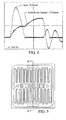
- FIGS. 2 and 3 illustrate the benefit of the PSD gate drive network. By properly tuning the network, positive PSD gate drive is assured throughout the PSD modulation period.
- FIG. 2 illustrates a typical PSD gate drive current waveform versus associated PSD cathode current with respect to time without a pulse capacitor connected (no high di/dt content).
- FIG. 3 illustrates a typical PSD gate drive current waveform versus associated PSD cathode current with respect to time with a pulse capacitor included in the circuit. In both cases, the PSD has positive gate drive during the cathode conduction period.
- FIG. 4 shows a typical PSD gate drive waveform without the associated gate drive network (diodes 148, 154 and inductor 150) included.
- the gate drive current waveform has higher amplitude, but considerably shorter duration. Due to the pulse nature of the circuit, the PSD does not have adequate time to properly latch and in fact is prevented from properly latching during the stressful high di/dt phase associated with the pulse network and consequently prone to premature failure due to gate current starvation and associated high power dissipation.
- a high amplitude high (di/dt) rate current is induced in the output pulse forming network 156 primary circuit elements comprised of the pulse capacitor 158 (approximately 0.05 microFarad) and a pulse transformer primary winding 160 of a transformer 162 having a secondary winding 164.
- the resonant tank circuit formed by capacitor 158 and transformer primary winding 160 induces a high tension damped sinusoidal waveform on the secondary winding 164 of pulse transformer 162 which is superimposed on the primary energy storage (tank) capacitor 100 potential creating a high potential output waveform to accomplish ionization of the igniter plug (not shown, but connected between Vout 166 and ground).
- the energy stored in the tank capacitor 100 induces a high di/dt current from ground 174 through capacitor 158 pulse transformer primary winding 160 to the negative side of the tank capacitor 100.
- the high di/dt negative polarity current creates a high frequency high amplitude oscillation in the secondary winding 164 for application to the spark plug gap.
- the L-C tank circuit comprised of the pulse transformer primary winding 160 and the pulse capacitor 158 controls the resonant frequency of the oscillation.
- the high amplitude oscillation is superimposed on the exciter tank capacitor voltage resulting in a high potential, high frequency waveform suitable to ionize the igniter plug spark gap allowing release of energy stored in the exciter tank circuit.
- the energy release can result in current of as much as 1500 amps flowing through the primary winding 160 of the pulse transformer, which is transformed to a level of approximately 15 kV to approximately 18 kV in the secondary winding 164 which is fed to the plug spark gap.
- a low impedance path is created between the igniter plug spark gap, the pulse transformer secondary winding 164, line 108, the tank capacitor 100, the node 106, the PSD 152 anode-cathode junction and circuit ground 168, allowing release of energy stored in tank capacitor 100 into the igniter plug spark plasma.
- Inductance of the pulse transformer secondary winding 164 controls the discharge rate and peak amplitude of the discharge waveform.
- a resistor 170 provides a load to absorb exciter discharge energy in the event of a quenched (open circuited) igniter.
- a resistor 172 bleeds charge off tank capacitor 100 to insure safe working voltages are present during product service.
- the circuitry contained in the Current Scheduling Circuitry block 24 reduces the current mode controller set point in response to abnormally low input voltages.
- the current scheduling circuitry enables exciter operation at input voltages significantly below normally specified input voltages, for example 6V.
- the superior leakage current performance of' the PSD switching device 152 enables such a solution. That is, current art ignition exciters are constrained by leakage currents at elevated temperatures. Consequently, current and past prior art ignition exciters intentionally charge the tank capacitor at the highest practical rate to minimize the chance of thermal runaway.
- PSD based exciters can reliably operate with considerably longer capacitor charge times at elevated temperatures. This allows introduction of a number of design features including smaller/lighter and lower cost EMI filters, charge pumps and input current scheduling circuitry to allow operation at extremely low input voltages.
- the current scheduling circuit adjusts the charge pump peak current set point of comparator 90 as a function of internal 8-volt bus voltage. As input voltage is reduced, the 8-volt regulator 16 drops out of regulation causing the 8V bus to droop.
- the current scheduling circuit comprised of transistors 180 and 182, Zener diode 184, resistors 186, 188, 190, 192, and 194, allows Zener diode 184 to conduct, holding the base of transistor 180, for example, at 3.9 volts.
- Transistor 180 operating in effect as a voltage follower, has an emitter voltage approximately 0.7 volts higher than its base voltage (or about 4.6 volts).
- Voltage divider 192/194 holds the base of transistor 182 at, for example, about 4.38 volts providing a base to emitter voltage for transistor 182 of about 0.22 volts preventing transistor 182 from conducting. There is no effect on the peak charge pump current for this condition.
- transistor 182 begins to conduct because its base voltage is derived from the 8-volt supply and the emitter voltage of 180 is held relatively constant by Zener diode 184.
- the collector current of transistor 182 develops a voltage across resistor 195adding to the actual current feedback voltage. This provides an "apparently" higher feedback voltage to the current mode comparator 90 forcing it to shut-off the transistor 84 at a lower peak current.
- transistor 182 collector current increases further reducing charge pump peak current.
- the voltage available to the circuit can't sustain transistor 182 collector current and the peak current setting will increase again.
- the charge pump will stop operating gracefully at an input voltage level incapable of providing adequate gate drive to the primary switching transistor 84.
- the voltage at which the circuit begins to reduce the peak current is set by the 192/194 voltage divider and the Zener diode 184, i.e., as the divider voltage approaches and becomes lower than the Zener diode 184 breakdown voltage, the circuit begins to supply current to 195, reducing peak current.
- Resistor 190 provides a convenient adjustment for gain (current reduction/supply voltage drop). Gain increases as the value of resistor 190 decreases.
- an exemplary PSD switching device gate-cathode metal pattern is illustrated.
- the highly interdigitated gate-cathode structure of this thyristor type device allows direct switching of high di/dt current pulses without the need for protective (saturable reactor) networks.
- the compact die footprint (preferably approximately 0.38 inches square) and thin base geometry improves switching speed by approximately 40% compared to competitive (approximately 0.5" diameter) pulse thyristor devices having a circular configuration.
- FIG. 6 illustrates a cross section of the PSD switching device, with portions removed, wherein the thickness of the structure is preferably only about 0.024 inches, with the (I) region approximately 0.018 inches
- the high resistivity to semi-insulating intrinsic region (I) reduces thermally generated carriers and corresponding leakage current at high ambient temperatures enabling improved ignition exciter performance at elevated ambient temperatures.
- the thin (approximately 0.020" thick) base width reduces forward voltage conduction losses approximately 35% relative to current prior art (0.040" thick) devices.
- bulk related leakage current is reduced an order of magnitude relative to competitive 0.040" thick (symmetric) structures.
- the high resistivity intrinsic region allows the PSD device to reliably block high voltages with a narrow base width relative to traditional thyristor structures.
- the narrow (approximately 0.020" thick) base structure and small (0.38" x 0.38") die size minimizes bulk and surface leakage currents while reducing device forward drop (conduction losses) and modulation time (switching losses) relative to current art technology.
- Measurements of PSD performance relative to current prior art technology confirm modulation rate is increased approximately 40%, while device forward conduction losses are reduced by approximately 35% and bulk leakage currents to approximately 10% of those associated with traditional high voltage thyristors. These benefits reduce device losses, improving circuit efficiency. Likewise, the improved efficiency results in lower device heating resulting in improved high temperature performance.
- the improved modulation rate allows simplification and miniaturization of the exciter pulse forming network due to improved magnetic coupling associated with the faster switching rate.
- the familiar Boltzmann factor of Equation 1 describes the effects of ambient temperature on intrinsic carrier concentration within a semiconductor.
- the highly intrinsic/semi-insulating layer reduces the total number of available carrier sites (Ns); reducing intrinsic carrier concentration relative to temperature.
- Exemplary PSD devices of the type described above exhibit leakage currents that are at least an order of magnitude lower than the best current art pulse thyristor technology enabling reliable operation at high ambient temperatures, for example up to approximately 175°C.
- FIG. 7 graphically illustrates the effect of ambient temperature on intrinsic carrier population in silicon.
- n i N s e (-Eg/2kBT)
- n i the intrinsic carrier concentration
- N s the number per unit volume of effectively available states; on the order of 10 9 /cc at 25°C
- leV 1.6022 x 10 -19 J k
- B Boltzmann's constant (1.381 x 10 -23 J/°K)
- T the absolute temperature in Kelvin
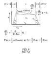
- FIGS. 8 and 9 show the relationship between carrier concentration and blocking voltage.
- FIG. 8 depicts current art n+pn-np++ structure where the peak electric field is 130 kV/cm severely limiting device breakdown voltage (the area under the E vs. x curve) and necessitating an inefficient wide base structure.
- FIG. 9 depicts an exemplary PSD type device using an approximately 10times higher dielectric breakdown material enabling a device potentially 10% of the thickness of a comparable breakdown voltage current art device.
- the first preferred embodiment of the present invention uses an intermediate tank circuit potential of approximately 1.8 kV to further improve exciter performance and reliability at elevated ambient temperatures.
- Industry standard current art aviation ignition exciter designs typically employ 2.5-3.5kV tank voltages.
- leakage current is further reduced at elevated ambient temperatures.
- the reduced exciter tank voltage requires fewer high voltage components, less insulation material and smaller physical flash & creep clearances; reducing unit weight, volume, and cost.
- PSD exciter EMI filter and charge pump
- FIG. 10 shows an oscillogram of a PSD based ignition exciter tank capacitor charge profile versus that of a typical solid state ignition exciter.
- the low PSD leakage current (on the order of 200 ⁇ A at approximately 135°C) allows operation at high ambient temperatures without threat of thermal runaway.
- traditional thyristors with leakage currents on the order of 5 mA at approximately 135°C require the use of more aggressive capacitor charge pump technology to prevent thermal runaway at high operating temperatures.
- 1 Hz rate exciter requires a power supply capable of delivering 66.7 W to achieve a 45 ms capacitor charge time.
- the same exciter requires only a 3.0 W power supply operating as a relaxation oscillator.
- the low peak input current associated with such a "continuous" charge cycle dramatically simplifies exciter charge pump and EMI filter design while reducing exciter cost, weight and volume.
- FIG. 1A While the first preferred embodiment that has been described with regard to FIG. 1 has a low side topology, a second preferred embodiment having a high side topology is shown in FIG. 1A.
- the capacitor 100 and PSD 152 are reversed relative to their positions in FIG. 1 which results in the capacitor 100 discharging positive voltage into the pulse transformer 162
- the tertiary winding 112 is not connected to ground but to capacitor 114 and line 108 and the direction of diode 110 is reversed.
- a third preferred embodiment is shown in the electrical circuit schematic diagram of FIG. 1B, which is very similar to the circuitry of the first preferred embodiment shown in FIG. 1, but is modified to operate together with an electronic engine controller (EEC) 200 that is frequently used to control aircraft turbine engines.
- EEC electronic engine controller
- a similar type of controller is also known in the art as FADEC controllers which is an acronym for a Full Authority Digital Engine Control. Such controllers are used to monitor a variety of parameters that are used to control the operation of aircraft engines as well as other systems of the aircraft as will be discussed.
- the exciter circuitry was typically connected to the aircraft power bus 100% of the time. Exciter activation and deactivation was then accomplished by providing logic level input signals to the exciter.
- the exciter input connector must contain a relatively high number of pins to facilitate input from each EEC channel. It has been typical that the EEC generally contain two redundant channels that must be capable of independently driving either exciter which necessitates a high number of input pins to allow redundant control of each ignition channel by the two EEC channels.
- the high pin count connector is generally more costly relative to a low pin count connector.
- the EEC controls the spark rate that is generated by the exciter circuit merely by selectively applying and terminating power to the exciter circuit via lines 202 and 204 which are connected to respective inputs 12 and 14.
- a diode 206 is provided at the output of a first portion of the power supply that provides a 28 volt source to the capacitor 48 and primary winding of the transformer 50. The diode 206 is intended to block reverse current flow when power has been terminated which would otherwise flow from the capacitor 48 and primary winding of the transformer 50 in the reverse direction. Since the charge pump circuitry 22 consists of integrated circuits and logic chips as well as switching transistors that are supplied by the 8 volt output bus from the regulator 16, when power is terminated by the EEC 200, this charge pump circuitry will be disabled.
- the internal circuitry of the charge pump 22 is also modified so that the zero output of the integrated circuit 58 does not clock the flip-flop 132. Rather, the clock input is supplied by a signal on clock line 208 that is connected to ground through a capacitor 210 and to the 8 volt power supply through resistor 212.
- the components 208, 210 and 212 define a one-shot multivibrator.
- the integrating circuit comprised of resistor 212 and capacitor 210 preferably has a relatively small RC time constant, e.g., about 1 millisecond, with respect to the anticipated capacitor 210 charge time interval which is approximately 60 milliseconds so that a charge/discharge sequence is initiated and then prevented until power is terminated and reapplied by the EEC.
- the EEC 200 thereby controls the power input bus voltage and can modulate the frequency of the output pulse of the igniter between the range of about 1 Hz to about 6 Hz. This modulation is effectively and desirably controlled by the EEC 200 because it receives other kinds of operating characteristic parameters concerning the engine.
- An advantage is that the spark rate of the exciter circuit is controlled only by the selective application and termination of power to the circuit rather than other control lines which would have to be protected from lighting and other EMI conditions.
- This embodiment enables improves turbine engine ignition flexibility by allowing the EEC to periodically pulse the exciter when sparks are required. By allowing the EEC to control the exciter, the system is more elegant than prior/current art systems that blindly generate sparks until power is removed. This feature improves effective igniter plug-wear and reduces stress on the exciter surface circuit and the aircraft electrical system. It also allows for more sophisticated system integration in that since the EEC already receives and processes a variety of environmental and electrical as well as physical measurements and subsequently controls a variety of engine parameters, it is ideally suited to evaluate engine parameters and command ignition as required.
- the EEC can command a higher spark rate during cold, or altitude relight regimes while protecting the exciter when the input voltage droops or the ambient temperature is too high.
- the EEC would preferably contain a map of allowable safe operating conditions and adjust the spark rate accordingly to protect the exciter circuit.
- FIG. 1C A fourth preferred embodiment is shown in FIG. 1C which is similar to FIG. 1, with the exception of the configuration of the resistor network 60, 62, 64 and 66 that are associated with the A, B, C and D inputs of the oscillator chip 58 of the charge pump 22.
- the 0_OUT line of the chip 58 is connected to clock the flip-flop 132 in the manner as described with respect to FIG. 1.
- the voltage regulator is a temperature compensated precision voltage reference that is used to provide a stable reference supply to the charge pump current and voltage mode comparators establish the VREF bus.
- This chip has a temperature output line 214 that is a voltage that is proportional to the ambient temperature of the chip 28.
- That signal on line 214 is applied to one input of the comparator 216, the other input of which is provided by line 218 that has voltage divider resistors 220 and 222.
- Line 218 is also connected to resistor 224 which in turn is connected to the 8V bus via resistor 226 and to an output line 228 that extends to the A input pin of the chip 58.
- the regulator 28 temperature output preferably has a positive temperature coefficient, delivering approximately 9.6 millivolts per °C above a baseline threshold. As the exciter internal temperature reaches a predetermined threshold, the comparator circuit pulls the output line 228 low which changes the divide-by-n value and effectively divides the exciter spark rate in half.
- the resistor 224 provides hysteresis which prevents oscillations around the set point temperature. In practice, the hysteresis may result in an approximately 10 to approximately 20°C deadband to prevent oscillation of the spark rate between the low and high repetition rates.
- the resistor 226 is a pull-up resistor required to force a logic 1 on pin A of the oscillator 58 until the comparator output pulls the pin low.
- FIG. ID an analog version of circuitry which adjusts the spark rate of the igniter is shown.
- the temperature output of the regulator 28 is connected to a voltage controlled oscillator 230 via lines 232 and the output of the VCO 230 is applied on line 234 to clock the flip-flop 132.
- the 0_OUT output pin of the chip 58 is not used to clock the flip-flop 132.
- the VCO oscillator frequency range is preferably tuned to reduce the spark rate as the ambient temperature increases.
- FIGS. 1B, 1C and 1D are modifications of the FIG. 1 circuitry, it should be understood that the same modifications can be made to the preferred embodiment shown in FIG. 1A inasmuch as the modifications of FIGS. 1B, C and D relate to the circuitry which is common to both of the first and second preferred embodiments shown in FIGS. 1 and 1A.
Landscapes
- Engineering & Computer Science (AREA)
- Chemical & Material Sciences (AREA)
- Combustion & Propulsion (AREA)
- Mechanical Engineering (AREA)
- General Engineering & Computer Science (AREA)
- Ignition Installations For Internal Combustion Engines (AREA)
Abstract
A turbine engine ignition exciter circuit applies energy stored in the exciter tank capacitor to the load (igniter plug) through a thyristor type semiconductor switching device that minimizes leakage current at elevated operating temperatures. The semiconductor switching device is periodically activated by a trigger circuit to initiate discharge of energy stored in exciter tank capacitor to mating ignition lead and igniter plug. The circuit operates at a modest, for example, approximately 1.8kV, tank circuit voltage to further reduce switching device leakage current related stresses at elevated temperatures allowing relatively long capacitor charge cycles, increased upper operating temperature capability and improved reliability. The circuit uses a low side switch circuit topology for releasing energy from said capacitor to ground whereby negative polarity energy is applied to the exciter. <IMAGE>
Description
The present invention generally relates to high voltage power supplies, and more
specifically to an improved ignition exciter for turbine engine applications.
Modern turbine engine ignition exciters, especially those used in small gas turbine
applications, have evolved considerably in recent years; migrating from spark gap
(plasma) switching devices and simple relaxation type oscillator charge pumps to more
reliable and predictable solid state switching devices with digitally controlled DC-DC
converter charge pumps. Thermal performance of current art solid state ignition exciters
has been limited due to available thyristor switching technology. Some designs use
multiple series stacked phase control thyristors with saturable reactors, while others
employ switching devices specifically designed for pulse power applications. However,
performance of both suffer from leakage current related limitations of the switching
devices. At elevated temperatures, leakage current within the switching device results in
increased power dissipation. This condition precipitates additional leakage current,
resulting in a thermal runaway condition and device failure.
The most advanced current art exciters employ pulse type thyristors to eliminate
the need for saturable magnetic components in the output stage and the associated
limitations of that technology. While a considerable improvement over phase control
based designs, thermal performance of current art pulse thyristor based ignition exciters
is still limited by switching device leakage current. Moreover, current art technology
incorporates costly semiconductor die manufacturing and device packaging techniques
limiting commercial viability of the ignition exciters. The ignition exciter embodiments
of the present invention exhibit superior reliability and have simplified gate circuitry
through the use of a unique low side switching topology.
The first preferred embodiment of the present invention provides improved turbine
engine ignition exciter technology that enables volumetrically efficient, lightweight, and
high reliability operation at elevated ambient temperatures. The first preferred
embodiment uses a semiconductor pulse switching device that is designed to exhibit low
leakage current at elevated ambient temperatures and a low side switching topology that
includes a discharge circuit for releasing energy from an energy store to ground whereby
negative polarity energy is applied to the igniter. This embodiment uses a gate drive
circuit that is specifically tuned for the particular exciter to insure a positive gate drive
current in the switching device throughout the stressful modulation period.
The first preferred embodiment also includes circuitry for compensating for low
input voltages applied to the exciter, which enables the exciter to reliably operate when
low input voltages are experienced.
A second preferred embodiment uses the semiconductor pulse switching device
that is designed to exhibit low leakage current at elevated ambient temperatures and a
high side switching topology that also uses a gate drive circuit that is specifically tuned
for the particular exciter to insure a positive gate drive current in the switching device
throughout the stressful modulation period.
Operation of current prior art turbine engine ignition exciters at elevated ambient
temperatures is limited by semiconductor leakage current. At elevated ambient
temperatures, semiconductor leakage current increases exponentially with temperature
which results in increased switching device power dissipation. This reduces product
reliability, and if not carefully accounted for in the design process, can result in system
failure due to thermal runaway effects. That is, at extreme temperatures device
dissipation causes further device heating, which in turn causes further dissipation which
progresses exponentially until the device is destroyed, This condition is exacerbated by
the relatively high (approximately 3 kV) exciter tank circuit voltages commonly used in
turbine engine ignition systems The first preferred embodiment of the present invention
employs a relatively low (i.e., approximately 1.5 kV to approximately 1.95 kV) tank
voltage to further reduce dielectric and leakage current stresses on the switching device.
Another advantage of the first preferred embodiment is the low side switching
circuit topology. Solid state turbine engine ignition exciters have traditionally employed
high side switching schemes to insure a positive polarity discharge waveform. Positive
polarity discharge waveforms are known to erode the negative polarity igniter plug outer
shell electrode at a higher rate than the positive polarity inner (center) electrode due to
positive ion bombardment. Typically, the igniter plug outer shell electrode is designed to
have considerably higher mass than the center electrode to maximize life. While the rate
of material erosion is highest on the negative polarity electrode, the rate of igniter plug
diametral spark gap growth is not appreciably different between positive and negative
polarity systems.
It has been determined that the igniter plug spark gap is on the order of 3% larger
at end of life using a negative polarity system on off-the-shelf igniters designed for
positive polarity systems. However, off-the-shelf igniters wear out at essentially the
same time regardless of ignition system polarity.
By contrast, positive polarity solid state ignition systems suffer a considerable
reliability penalty due to the fact the switching device cathode is referenced to a dynamic
load. That is, prior to igniter plug ionization, the cathode is essentially floating with
respect to circuit ground. This condition makes it difficult to insure a predictable and
repeatable switching device gate drive during the stressful device modulation period.
The first preferred embodiment of the present invention solves this problem by
referencing the switching device cathode to circuit ground. In this topology, the gate
drive waveform is highly predictable and repeatable and can be easily controlled with
simple and inexpensive circuitry.
The preferred embodiments of the present invention also include novel circuitry to
schedule input current allowing reliable operation at low input voltages. Recent trends in
turbine engine based aircraft have resulted in lower available input voltage at engine start.
Modern small gas turbine ignition exciters typically employ current mode pulse width
modulator (PWM) based DC-DC converters to accomplish the capacitor charging
function. At very low input voltages, the current mode controller set point value cannot
be satisfied, resulting in a continuous current drain. To prevent this condition, the
preferred embodiments employ current scheduling circuitry to automatically adjust the
PWM set point as a function of input voltage allowing operation at low input voltages.
Turning now to the drawings and particularly FIG. 1, the first preferred
embodiment of the ignition exciter circuit is illustrated generally at 10. It will be
appreciated by those skilled in the art that the essential discharge circuit elements of the
exemplary embodiment can easily be adapted, for example, to ac input power variants
and various application specific output voltage, spark rate and energy configurations.
The power supply section is comprised of two individual voltage regulator
sections. Both derive power at 12 and 14 from the exciter input power source and
subsequent electromagnetic interference filter (both, not illustrated). The first regulator,
comprised of integrated circuit 16, capacitors 18 and 20 provides power to the exciter
internal circuitry (charge pump circuitry, indicated generally at 22, current scheduling
circuitry, indicated generally at 24, and discharge circuitry, indicated generally at 26,
establishing the +8V bus. The other regulator, comprised of integrated circuit 28 and
capacitors 30, 32 and 34 is a temperature compensated precision voltage reference used
to provide a stable reference supply to the charge pump current and voltage mode
comparators establishing the Vref bus. The reference supply is designed to insure
predictable (spec. compliant) operation of the ignition exciter at extremely low input
voltages (for example 8.5VDC). Other elements within the power supply section include,
a reverse polarity protection diode 36; capacitor 38, resistor 40 and transorb 42, EMI
suppression and transient input voltage protection elements 44 and fuse 46 primary dc
power bus fault protection.
The charge pump section 22 is a current mode flyback topology DC-DC converter.
Filtered input power supplied to the charge pump from the input power source and EMI
filter (not illustrated) is stored on energy reservoir capacitors 48 in the upper right portion
of the charge pump section 22. This capacitor sources current to the primary winding of
a flyback transformer 50 through line 52 minimizing current drain on the input power bus
during charge pump 22 operation.
The high frequency (charge pump rate) output from integrated circuit 58, which is
preferably on the order of 90 kHz, but which can be higher or lower, is routed via line 70
to flip-flop 72. A totem pole gate drive circuit comprised of transistors 74, 76, resistors
78, 80 and capacitor 82 in turn activates transistor 84 in response to signals provided by
flip-flop 72. When activated, transistor 84 initiates current flow from the DC input bus
(+28V) through transistor 84 and the current mode sense resistor resistor 86. As current
flow linearly ramps up through the transformer primary winding, an analogous voltage is
generated on the sense resistor 86 which is applied by line 88 to the positive input of a
comparator 90, which operates as a current mode controller with associated reference
voltage divider resistors 92 and 94. The comparator 90 resets flip-flop 72 via line 96
when the appropriate input current value is achieved. This in turn terminates the current
mode cycle insuring precise control of the transformer 50 energy (E= LI2/2) on a per
cycle basis.
The charge pump has two independent outputs. The primary output is the
secondary of the flyback transformer 50 which charges the exciter main energy storage
(tank) capacitor 100 via line 102 which has four series connected rectifier diodes 104
and node 106 that is connected to the positive terminal of the capacitor 100, with the
negative terminal thereof being connected to ground via line 108 and diode 110. A
second, tertiary, winding 112 on the flyback transformer 50 similarly charges a tertiary
energy storage capacitor 114 through rectifier diode 116, resistor 118 and line 120. As
the charge pump operates, charge is incrementally imparted on the tank capacitor 100 and
the tertiary capacitor 114, increasing the potential on each capacitor approximately as a
function of the transformer secondary-tertiary turns ratio. Therefore, the tertiary tank
capacitor 114 circuit forms a low potential mirror of the high potential primary energy
storage tank capacitor 100 circuit allowing safe, reliable and indirect monitoring of the
high potential circuit.
A voltage mode feedback loop comprised primarily of line 120, comparator 122,
associated reference divider resistors 124 and 126 and feedback resistor divider 128 and
130 monitors the tertiary tank capacitor 114 to determine when both capacitors have
reached full charge. When the tertiary tank capacitor 114 voltage feedback signal reaches
the set point value, comparator 122 resets flip-flop 132 via line 134. This prevents
transmission of high frequency (charge pump rate) flip-flop 72 drive signal to the
switching transistor 84; deactivating the high frequency charge pump operation.
Likewise, this condition causes flip flop 132 to simultaneously transmit a trigger signal
via line 136 to transistor 138 in the discharge circuit 26.
The trigger signal from flip flop 132 on line 136 activates switching transistor 138
allowing charge stored in a trigger tank capacitor 140 to discharge to ground through a
trigger transformer 142. This activity in turn generates a trigger pulse through diode 144
which activates the gate drive of thyristor 146. The thyristor 146 then conducts charge
stored in the tertiary tank capacitor 114 which preferably has a capacity of 30 mJ, so that
a current of on the order of 35 amperes may flow through rectifier diode 148, inductor
150 into the gate-cathode junction of a PSD (Pulse Switching Device) 152. The gate
drive circuit comprised of rectifier diode 148, inductor 150 and a rectifier diode 154 is
specifically tuned for the particular exciter to insure a positive PSD gate drive current
throughout the stressful PSD modulation period. Specifically, inductor 150 is tuned to
account for differences in the exciter stored energy (tank capacitor 100 value) and
resonant frequency of an output pulse forming network indicated generally at 156 to
prevent zero, or negative bias on the PSD 152 gate terminal improving PSD reliability
and performance. The negative polarity PSD circuit topology and associated gate drive
circuitry significantly reduces dielectric stress on the gate drive circuitry since the
circuitry is referenced to ground and does not modulate from ground potential to the
exciter tank voltage during discharge.
FIGS. 2 and 3 illustrate the benefit of the PSD gate drive network. By properly
tuning the network, positive PSD gate drive is assured throughout the PSD modulation
period. FIG. 2 illustrates a typical PSD gate drive current waveform versus associated
PSD cathode current with respect to time without a pulse capacitor connected (no high
di/dt content). FIG. 3 illustrates a typical PSD gate drive current waveform versus
associated PSD cathode current with respect to time with a pulse capacitor included in the
circuit. In both cases, the PSD has positive gate drive during the cathode conduction
period. By contrast, FIG. 4 shows a typical PSD gate drive waveform without the
associated gate drive network ( diodes 148, 154 and inductor 150) included. In the latter
case, the gate drive current waveform has higher amplitude, but considerably shorter
duration. Due to the pulse nature of the circuit, the PSD does not have adequate time to
properly latch and in fact is prevented from properly latching during the stressful high
di/dt phase associated with the pulse network and consequently prone to premature
failure due to gate current starvation and associated high power dissipation.
Referring again to FIG. 1, when the PSD 152 is activated, a high amplitude high
(di/dt) rate current is induced in the output pulse forming network 156 primary circuit
elements comprised of the pulse capacitor 158 (approximately 0.05 microFarad) and a
pulse transformer primary winding 160 of a transformer 162 having a secondary winding
164. The resonant tank circuit formed by capacitor 158 and transformer primary winding
160 induces a high tension damped sinusoidal waveform on the secondary winding 164
of pulse transformer 162 which is superimposed on the primary energy storage (tank)
capacitor 100 potential creating a high potential output waveform to accomplish
ionization of the igniter plug (not shown, but connected between Vout 166 and ground).
When the PSD 152 is switched on, the energy stored in the tank capacitor 100
induces a high di/dt current from ground 174 through capacitor 158 pulse transformer
primary winding 160 to the negative side of the tank capacitor 100. The high di/dt
negative polarity current creates a high frequency high amplitude oscillation in the
secondary winding 164 for application to the spark plug gap. The L-C tank circuit
comprised of the pulse transformer primary winding 160 and the pulse capacitor 158
controls the resonant frequency of the oscillation. The high amplitude oscillation is
superimposed on the exciter tank capacitor voltage resulting in a high potential, high
frequency waveform suitable to ionize the igniter plug spark gap allowing release of
energy stored in the exciter tank circuit.
The energy release can result in current of as much as 1500 amps flowing through
the primary winding 160 of the pulse transformer, which is transformed to a level of
approximately 15 kV to approximately 18 kV in the secondary winding 164 which is fed
to the plug spark gap. When the igniter plug spark gap is ionized, a low impedance path
is created between the igniter plug spark gap, the pulse transformer secondary winding
164, line 108, the tank capacitor 100, the node 106, the PSD 152 anode-cathode junction
and circuit ground 168, allowing release of energy stored in tank capacitor 100 into the
igniter plug spark plasma. Inductance of the pulse transformer secondary winding 164
controls the discharge rate and peak amplitude of the discharge waveform. A resistor 170
provides a load to absorb exciter discharge energy in the event of a quenched (open
circuited) igniter. A resistor 172 bleeds charge off tank capacitor 100 to insure safe
working voltages are present during product service.
Another feature of the first preferred embodiment of the present invention is a
novel current mode scheduling circuit. Referring to FIG. 1, the circuitry contained in the
Current Scheduling Circuitry block 24 reduces the current mode controller set point in
response to abnormally low input voltages. Unlike current art solutions directed toward
deactivation of the exciter circuitry when input voltage falls below a prescribed threshold
level, the current scheduling circuitry enables exciter operation at input voltages
significantly below normally specified input voltages, for example 6V. The superior
leakage current performance of' the PSD switching device 152 enables such a solution.
That is, current art ignition exciters are constrained by leakage currents at elevated
temperatures. Consequently, current and past prior art ignition exciters intentionally
charge the tank capacitor at the highest practical rate to minimize the chance of thermal
runaway. By contrast, PSD based exciters can reliably operate with considerably longer
capacitor charge times at elevated temperatures. This allows introduction of a number of
design features including smaller/lighter and lower cost EMI filters, charge pumps and
input current scheduling circuitry to allow operation at extremely low input voltages.
Functionally, the current scheduling circuit adjusts the charge pump peak current
set point of comparator 90 as a function of internal 8-volt bus voltage. As input voltage is
reduced, the 8-volt regulator 16 drops out of regulation causing the 8V bus to droop.
When the 8V bus is operating normally, the current scheduling circuit comprised of
transistors 180 and 182, Zener diode 184, resistors 186, 188, 190, 192, and 194, allows
Zener diode 184 to conduct, holding the base of transistor 180, for example, at 3.9 volts.
Transistor 180, operating in effect as a voltage follower, has an emitter voltage
approximately 0.7 volts higher than its base voltage (or about 4.6 volts). Voltage divider
192/194 holds the base of transistor 182 at, for example, about 4.38 volts providing a
base to emitter voltage for transistor 182 of about 0.22 volts preventing transistor 182
from conducting. There is no effect on the peak charge pump current for this condition.
As the 8-volt bus drops out of regulation, transistor 182 begins to conduct because its
base voltage is derived from the 8-volt supply and the emitter voltage of 180 is held
relatively constant by Zener diode 184. The collector current of transistor 182 develops a
voltage across resistor 195adding to the actual current feedback voltage. This provides an
"apparently" higher feedback voltage to the current mode comparator 90 forcing it to
shut-off the transistor 84 at a lower peak current. As the 8-volt output continues to drop,
transistor 182 collector current increases further reducing charge pump peak current. As
the 8-volt supply continues to fall, the voltage available to the circuit can't sustain
transistor 182 collector current and the peak current setting will increase again. Through
careful design, the charge pump will stop operating gracefully at an input voltage level
incapable of providing adequate gate drive to the primary switching transistor 84.
It will be appreciated by those skilled in the art, one can easily modify the circuit
"characteristics", gains and levels, by changing component values. The voltage at which
the circuit begins to reduce the peak current is set by the 192/194 voltage divider and the
Zener diode 184, i.e., as the divider voltage approaches and becomes lower than the
Zener diode 184 breakdown voltage, the circuit begins to supply current to 195, reducing
peak current. Resistor 190 provides a convenient adjustment for gain (current
reduction/supply voltage drop). Gain increases as the value of resistor 190 decreases.
Referring to FIG. 5, an exemplary PSD switching device gate-cathode metal
pattern is illustrated. The highly interdigitated gate-cathode structure of this thyristor
type device allows direct switching of high di/dt current pulses without the need for
protective (saturable reactor) networks. The compact die footprint (preferably
approximately 0.38 inches square) and thin base geometry improves switching speed by
approximately 40% compared to competitive (approximately 0.5" diameter) pulse
thyristor devices having a circular configuration.
FIG. 6 illustrates a cross section of the PSD switching device, with portions
removed, wherein the thickness of the structure is preferably only about 0.024 inches,
with the (I) region approximately 0.018 inches The high resistivity to semi-insulating
intrinsic region (I) reduces thermally generated carriers and corresponding leakage
current at high ambient temperatures enabling improved ignition exciter performance at
elevated ambient temperatures. The thin (approximately 0.020" thick) base width
reduces forward voltage conduction losses approximately 35% relative to current prior art
(0.040" thick) devices. Similarly, bulk related leakage current is reduced an order of
magnitude relative to competitive 0.040" thick (symmetric) structures.
The high resistivity intrinsic region allows the PSD device to reliably block high
voltages with a narrow base width relative to traditional thyristor structures. The narrow
(approximately 0.020" thick) base structure and small (0.38" x 0.38") die size minimizes
bulk and surface leakage currents while reducing device forward drop (conduction losses)
and modulation time (switching losses) relative to current art technology. Measurements
of PSD performance relative to current prior art technology confirm modulation rate is
increased approximately 40%, while device forward conduction losses are reduced by
approximately 35% and bulk leakage currents to approximately 10% of those associated
with traditional high voltage thyristors. These benefits reduce device losses, improving
circuit efficiency. Likewise, the improved efficiency results in lower device heating
resulting in improved high temperature performance. Moreover, the improved
modulation rate allows simplification and miniaturization of the exciter pulse forming
network due to improved magnetic coupling associated with the faster switching rate.
The familiar Boltzmann factor of Equation 1 describes the effects of ambient
temperature on intrinsic carrier concentration within a semiconductor. The highly
intrinsic/semi-insulating layer reduces the total number of available carrier sites (Ns);
reducing intrinsic carrier concentration relative to temperature. Exemplary PSD devices
of the type described above exhibit leakage currents that are at least an order of
magnitude lower than the best current art pulse thyristor technology enabling reliable
operation at high ambient temperatures, for example up to approximately 175°C. FIG. 7
graphically illustrates the effect of ambient temperature on intrinsic carrier population in
silicon.
ni = Ns e(-Eg/2kBT)
Where,
ni = the intrinsic carrier concentration
Ns = the number per unit volume of effectively available states; on the order of 109/cc at 25°C
Eg = the material energy gap (Si= 1.17 - (4.73 · 10-4 · T2/(T+636)) eV) NOTE: leV=1.6022 x 10⁻¹⁹ J
kB = Boltzmann's constant (1.381 x 10⁻²³ J/°K)
T = the absolute temperature in Kelvin
By decreasing carrier concentration in the intrinsic layer; transitioning between
standard doping levels to, for example, highly intrinsic or semi-insulating levels,
increased blocking voltage can be achieved for a given base width. FIGS. 8 and 9 show
the relationship between carrier concentration and blocking voltage. Using simple
breakdown calculations where the breakdown voltage is approximated by calculating the
area underneath the electric field line, FIG. 8 depicts current art n+pn-np++ structure
where the peak electric field is 130 kV/cm severely limiting device breakdown voltage
(the area under the E vs. x curve) and necessitating an inefficient wide base structure.
By contrast, FIG. 9 depicts an exemplary PSD type device using an approximately
10times higher dielectric breakdown material enabling a device potentially 10% of the
thickness of a comparable breakdown voltage current art device. By employing the
highly resistive or semi-insulating intrinsic layer, PSD switching speed, forward
conduction losses and leakage current are all improved over current art technology.
The first preferred embodiment of the present invention uses an intermediate tank
circuit potential of approximately 1.8 kV to further improve exciter performance and
reliability at elevated ambient temperatures. Industry standard current art aviation
ignition exciter designs typically employ 2.5-3.5kV tank voltages. By reducing the
blocking voltage requirements of the switching device, leakage current is further reduced
at elevated ambient temperatures. The reduced exciter tank voltage requires fewer high
voltage components, less insulation material and smaller physical flash & creep
clearances; reducing unit weight, volume, and cost.
Another key improvement enabled by PSD technology is simplification of the
exciter EMI filter and charge pump (DC-DC converter) circuitry. Current prior art solid
state ignition exciters are severely limited by switching device leakage current and
junction temperature capability. Consequently, current prior art exciters employ large,
bulky EMI filters and charge pump circuits to minimize tank capacitor charge time. That
is, by minimizing the time the switching device is exposed to stressful high voltage
blocking condition; particularly at high ambient temperatures, the exciter is capable of
operating at high ambient temperatures. By contrast, due to the exceptionally low PSD
leakage current at elevated temperatures and high junction temperature capability, the
exciter capacitor charge time is less critical allowing miniaturization and simplification of
the EMI filter and charge pump circuitry. FIG. 10 shows an oscillogram of a PSD based
ignition exciter tank capacitor charge profile versus that of a typical solid state ignition
exciter. The low PSD leakage current (on the order of 200µA at approximately 135°C)
allows operation at high ambient temperatures without threat of thermal runaway. By
contrast traditional thyristors with leakage currents on the order of 5 mA at
approximately 135°C require the use of more aggressive capacitor charge pump
technology to prevent thermal runaway at high operating temperatures. For example, a
typical 3.0 J (stored energy), 1 Hz rate exciter requires a power supply capable of
delivering 66.7 W to achieve a 45 ms capacitor charge time. By contrast, the same
exciter requires only a 3.0 W power supply operating as a relaxation oscillator. The low
peak input current associated with such a "continuous" charge cycle dramatically
simplifies exciter charge pump and EMI filter design while reducing exciter cost, weight
and volume.
While the first preferred embodiment that has been described with regard to FIG. 1
has a low side topology, a second preferred embodiment having a high side topology is
shown in FIG. 1A. In this embodiment, the capacitor 100 and PSD 152 are reversed
relative to their positions in FIG. 1 which results in the capacitor 100 discharging positive
voltage into the pulse transformer 162 Also, the tertiary winding 112 is not connected to
ground but to capacitor 114 and line 108 and the direction of diode 110 is reversed.
A third preferred embodiment is shown in the electrical circuit schematic diagram
of FIG. 1B, which is very similar to the circuitry of the first preferred embodiment shown
in FIG. 1, but is modified to operate together with an electronic engine controller (EEC)
200 that is frequently used to control aircraft turbine engines. A similar type of controller
is also known in the art as FADEC controllers which is an acronym for a Full Authority
Digital Engine Control. Such controllers are used to monitor a variety of parameters that
are used to control the operation of aircraft engines as well as other systems of the aircraft
as will be discussed.
Existing FADEC's and EEC's are known to control the spark rate, but it is done
by control lines to the exciter circuit rather than the power lines that are used to power the
exciter circuit. Because of the potential of lightning strikes and other electro-magnetic
interference, it has been necessary to employ extensive EMI filters and the like on the
front end to protect all of the signal lines that are used to control the exciter circuit,
In prior art EEC controlled ignition systems, the exciter circuitry was typically
connected to the aircraft power bus 100% of the time. Exciter activation and deactivation
was then accomplished by providing logic level input signals to the exciter. In this
arrangement, the exciter input connector must contain a relatively high number of pins to
facilitate input from each EEC channel. It has been typical that the EEC generally
contain two redundant channels that must be capable of independently driving either
exciter which necessitates a high number of input pins to allow redundant control of each
ignition channel by the two EEC channels. The high pin count connector is generally
more costly relative to a low pin count connector.
In this preferred embodiment, the EEC controls the spark rate that is generated by
the exciter circuit merely by selectively applying and terminating power to the exciter
circuit via lines 202 and 204 which are connected to respective inputs 12 and 14. A diode
206 is provided at the output of a first portion of the power supply that provides a 28 volt
source to the capacitor 48 and primary winding of the transformer 50. The diode 206 is
intended to block reverse current flow when power has been terminated which would
otherwise flow from the capacitor 48 and primary winding of the transformer 50 in the
reverse direction. Since the charge pump circuitry 22 consists of integrated circuits and
logic chips as well as switching transistors that are supplied by the 8 volt output bus from
the regulator 16, when power is terminated by the EEC 200, this charge pump circuitry
will be disabled. The internal circuitry of the charge pump 22 is also modified so that the
zero output of the integrated circuit 58 does not clock the flip-flop 132. Rather, the clock
input is supplied by a signal on clock line 208 that is connected to ground through a
capacitor 210 and to the 8 volt power supply through resistor 212. The components 208,
210 and 212 define a one-shot multivibrator.
When the voltage on the input power bus on inputs 12 and 14 is interrupted, the
substantial charge on capacitor 48 will tend to move back to the voltage regulator 16
were it not for the diode 206 which blocks that reverse flow. In this manner, the 8 volt
and VREF regulators 16 and 28 will decay very quickly and when they do decay, the flip-flop
72, one-shot multivibrator 132 as well as comparator 90 will go dead which
effectively resets these components. Since the output from chip 58 that was used in the
embodiments of FIGS. 1 and 1A is no longer being used, the new one-shot 132 type of
operation will cause the one-shot to be clocked when the capacitor 210 is charged upon
resumption of input power to the input power bus 12 and 14. The integrating circuit
comprised of resistor 212 and capacitor 210 preferably has a relatively small RC time
constant, e.g., about 1 millisecond, with respect to the anticipated capacitor 210 charge
time interval which is approximately 60 milliseconds so that a charge/discharge sequence
is initiated and then prevented until power is terminated and reapplied by the EEC. The
EEC 200 thereby controls the power input bus voltage and can modulate the frequency of
the output pulse of the igniter between the range of about 1 Hz to about 6 Hz. This
modulation is effectively and desirably controlled by the EEC 200 because it receives
other kinds of operating characteristic parameters concerning the engine. An advantage
is that the spark rate of the exciter circuit is controlled only by the selective application
and termination of power to the circuit rather than other control lines which would have
to be protected from lighting and other EMI conditions.
This embodiment enables improves turbine engine ignition flexibility by allowing
the EEC to periodically pulse the exciter when sparks are required. By allowing the EEC
to control the exciter, the system is more elegant than prior/current art systems that
blindly generate sparks until power is removed. This feature improves effective igniter
plug-wear and reduces stress on the exciter surface circuit and the aircraft electrical
system. It also allows for more sophisticated system integration in that since the EEC
already receives and processes a variety of environmental and electrical as well as
physical measurements and subsequently controls a variety of engine parameters, it is
ideally suited to evaluate engine parameters and command ignition as required. For
example, the EEC can command a higher spark rate during cold, or altitude relight
regimes while protecting the exciter when the input voltage droops or the ambient
temperature is too high. In the latter case, the EEC would preferably contain a map of
allowable safe operating conditions and adjust the spark rate accordingly to protect the
exciter circuit.
A fourth preferred embodiment is shown in FIG. 1C which is similar to FIG. 1,
with the exception of the configuration of the resistor network 60, 62, 64 and 66 that are
associated with the A, B, C and D inputs of the oscillator chip 58 of the charge pump 22.
In this configuration, the 0_OUT line of the chip 58 is connected to clock the flip-flop
132 in the manner as described with respect to FIG. 1. As previously mentioned, the
voltage regulator is a temperature compensated precision voltage reference that is used to
provide a stable reference supply to the charge pump current and voltage mode
comparators establish the VREF bus. This chip has a temperature output line 214 that is
a voltage that is proportional to the ambient temperature of the chip 28. That signal on
line 214 is applied to one input of the comparator 216, the other input of which is
provided by line 218 that has voltage divider resistors 220 and 222. Line 218 is also
connected to resistor 224 which in turn is connected to the 8V bus via resistor 226 and to
an output line 228 that extends to the A input pin of the chip 58.
The regulator 28 temperature output preferably has a positive temperature
coefficient, delivering approximately 9.6 millivolts per °C above a baseline threshold. As
the exciter internal temperature reaches a predetermined threshold, the comparator circuit
pulls the output line 228 low which changes the divide-by-n value and effectively divides
the exciter spark rate in half. The resistor 224 provides hysteresis which prevents
oscillations around the set point temperature. In practice, the hysteresis may result in an
approximately 10 to approximately 20°C deadband to prevent oscillation of the spark rate
between the low and high repetition rates. The resistor 226 is a pull-up resistor required
to force a logic 1 on pin A of the oscillator 58 until the comparator output pulls the pin
low. In this manner, discrete changes in the spark rate control can be achieved. It should
be understood that multistage digital versions could be employed by adding other
comparators in a manner that is well known to those of ordinary skill in the art which
would divide the spark rate by 2 and then by 2 again which could result in output rates of
1,2 or 4 Hz.
Referring to FIG. ID, an analog version of circuitry which adjusts the spark rate of
the igniter is shown. In this embodiment, the temperature output of the regulator 28 is
connected to a voltage controlled oscillator 230 via lines 232 and the output of the VCO
230 is applied on line 234 to clock the flip-flop 132. In this embodiment it is apparent
that the 0_OUT output pin of the chip 58 is not used to clock the flip-flop 132. The VCO
oscillator frequency range is preferably tuned to reduce the spark rate as the ambient
temperature increases.
While the embodiments shown in FIGS. 1B, 1C and 1D are modifications of the
FIG. 1 circuitry, it should be understood that the same modifications can be made to the
preferred embodiment shown in FIG. 1A inasmuch as the modifications of FIGS. 1B, C
and D relate to the circuitry which is common to both of the first and second preferred
embodiments shown in FIGS. 1 and 1A.
While various embodiments of the present invention have been shown and
described, it should be understood that other modifications, substitutions and alternatives
are apparent to one of ordinary skill in the art. Such modifications, substitutions and
alternatives can be made without departing from the spirit and scope of the invention,
which should be determined from the appended claims.
Various features of the invention are set forth in the following claims.
Various features of the invention are set forth in the following claims.
Where technical features mentioned in any claim are followed by reference signs,
those reference signs have been included for the sole purpose of increasing the
intelligibility of the claims and accordingly, such reference signs do not have any limiting
effect on the interpretation of each element identified by way of example by such
reference signs.
Claims (11)
- An exciter circuit (10) for use with an igniter for creating a spark for igniting fuel in an engine; comprising:a charge pump circuit (22) for selectively applying power to an input of a voltage conversion device (50) having a first output, said device being configured to step-up a first voltage level applied to said input to a higher second voltage level at said first output;a main energy store (100) having positive and negative terminals, said positive terminal being connected in circuit to said first output for receiving energy from said charge pump circuit, said negative terminal being connected to the igniter via a ground loop circuit having a step-up pulse transformer (156) therein;a semiconductor switch (152) having an anode, a cathode and a gate for controlling the release of energy from said main energy store, said cathode being connected to ground and said anode being connected to said positive main energy store terminal; and,a trigger circuit (138, 140, 142, 144, 146, 114, 148, 150) connected to said charge pump circuit and to said gate and selectively applying a trigger signal to said gate for placing said switch into conduction thereby discharging said energy store to ground, said ground loop circuit producing negative current through said step-up pulse transformer to said negative terminal and thereby creating a high voltage pulse that is applied to the igniter for creating a spark.
- An exciter circuit as defined in claim 1 wherein said voltage conversion device has a second output with a higher third voltage level and said trigger circuit further comprises a tertiary energy store that supplies said trigger signal to said gate via a trigger switch having a control input, said trigger switch being placed into conduction when an actuating signal is received from said charge pump circuit.
- An exciter circuit as defined in claim 2 wherein said trigger circuit further comprises:a first diode having its anode connected to said tertiary energy store and its cathode connected in series to an inductor that is connected in series with said gate; anda second diode that has its cathode connected to said inductor and to said first diode cathode, said second diode having its anode connected to ground;said first and second diodes and said inductor being tuned to insure positive current flow to said gate during the turn-on time period of said semiconductor switch.
- An exciter circuit as defined in claim 1 further comprising a power supply circuit that is connectable to an external source of input power and provides a DC output having said first voltage level, a second lower internal voltage bus and a third temperature compensated precision reference voltage.
- An exciter circuit as defined in claim 4 wherein said voltage conversion device is a transformer having a primary winding as said input, said charge pump circuit further comprising:a switching transistor connected in series between a power source of said first voltage, said primary winding, a voltage sensing resistor and ground;logic circuitry for switching said switching transistor in and out of conduction:comparator circuitry connected to said switching transistor for comparing the voltage level of said voltage sensing resistor to a reference voltage and switching said transistor out of conduction when said voltage level exceeds said reference level.
- An exciter circuit as defined in claim 5 further comprising scheduling circuitry for adjusting the voltage level of said voltage sensing resistor in proportion to a drop in said internal voltage bus so that operation of said charge pump circuit continues notwithstanding said internal voltage bus voltage drop.
- An exciter circuit as defined in claim 5 wherein said charge pump circuit further comprises second comparator circuitry operably connected to said trigger circuit for monitoring the voltage level of said tertiary energy store and for controlling said logic circuitry to switch said transistor out of conduction when said voltage of said tertiary energy store reaches a predetermined level.
- An exciter circuit as defined in claim 1 wherein said second voltage level is within the range of about 1500 to about 1950 volts DC.
- An exciter circuit as defined in claim 1 wherein said high voltage pulse has a magnitude within the range of about -15,000 to about -18,000 volts.
- An exciter circuit for use with an igniter for creating a spark for igniting fuel in a turbine engine; comprising:at least one energy storing device for storing energy that is released to the igniter for creating the spark for igniting fuel in the turbine engine;a charging circuit for storing energy in the energy store;a discharge circuit including a semiconductor switch having an anode, a cathode and a gate, said switch controlling the release of energy from said energy store, said cathode being directly connected to ground and said anode being connected to said positive energy store terminal, a step-up pulse transformer with a primary winding connected to said negative terminal and to ground through a capacitor and a secondary winding connected to the igniter;a trigger circuit for placing said semiconductor switch into conduction, thereby discharging said energy store to ground and producing a negative current through said step-up pulse transformer to said negative terminal and thereby creating a negative high voltage pulse that is applied to the igniter for creating the spark.
- An exciter circuit as defined in claim 10 wherein said primary winding and capacitor comprise a first leg, said discharge circuit further comprising a resister leg and a diode leg connected in parallel said first leg, said diode having its cathode connected to ground.
Applications Claiming Priority (2)
| Application Number | Priority Date | Filing Date | Title |
|---|---|---|---|
| US868621 | 2004-06-15 | ||
| US10/868,621 US7355300B2 (en) | 2004-06-15 | 2004-06-15 | Solid state turbine engine ignition exciter having elevated temperature operational capability |
Publications (1)
| Publication Number | Publication Date |
|---|---|
| EP1607622A2 true EP1607622A2 (en) | 2005-12-21 |
Family
ID=34940155
Family Applications (1)
| Application Number | Title | Priority Date | Filing Date |
|---|---|---|---|
| EP05105178A Withdrawn EP1607622A2 (en) | 2004-06-15 | 2005-06-14 | A solid state turbine engine ignition exciter having elevated temperature operational capability |
Country Status (3)
| Country | Link |
|---|---|
| US (1) | US7355300B2 (en) |
| EP (1) | EP1607622A2 (en) |
| JP (1) | JP2006002771A (en) |
Cited By (2)
| Publication number | Priority date | Publication date | Assignee | Title |
|---|---|---|---|---|
| EP1834083A4 (en) * | 2004-12-23 | 2010-09-29 | Pratt & Whitney Canada Corp Pr | Variable rate ignition |
| EP4382741A3 (en) * | 2022-12-08 | 2024-07-17 | Hamilton Sundstrand Corporation | Engine ignition systems and control methods therefor |
Families Citing this family (16)
| Publication number | Priority date | Publication date | Assignee | Title |
|---|---|---|---|---|
| US8266885B2 (en) * | 2008-12-23 | 2012-09-18 | General Electric Company | Method and systems for adaptive ignition energy |
| US8305049B2 (en) * | 2009-04-06 | 2012-11-06 | Hamilton Sundstrand Corporation | Starter voltage reducing synchronous machine |
| US8530902B2 (en) * | 2011-10-26 | 2013-09-10 | General Electric Company | System for transient voltage suppressors |
| US20130146708A1 (en) * | 2011-12-08 | 2013-06-13 | Honeywell International Inc. | Case assemblies with common controls |
| US9622331B2 (en) | 2012-12-26 | 2017-04-11 | Unison Industries, Llc | Discharge switch device for ignition excitation system |
| CN104097595B (en) * | 2013-04-07 | 2016-09-14 | 王刚 | Box is controlled based on monolithic processor controlled automobile starting |
| US9488130B2 (en) | 2013-10-17 | 2016-11-08 | Honeywell International Inc. | Variable area fan nozzle systems with improved drive couplings |
| FR3015571B1 (en) * | 2013-12-23 | 2018-11-23 | Safran Helicopter Engines | METHOD AND SYSTEM FOR RELIABLY STARTING TURBOMACHINE |
| US9399954B2 (en) * | 2014-03-17 | 2016-07-26 | Unison Industries, Llc | Ignition exciter discharge switch |
| US10473033B2 (en) * | 2016-10-19 | 2019-11-12 | Honeywell International Inc. | Gas turbine engine |
| US10801414B2 (en) * | 2017-01-24 | 2020-10-13 | Honeywell International Inc. | Gas turbine engine including a rectifierless electronic control unit and method for supplying power to same |
| CN109458260B (en) * | 2018-11-28 | 2020-12-08 | 陕西航空电气有限责任公司 | Discharge trigger holding circuit of variable-frequency and variable-energy ignition device of aircraft engine |
| CN111120112B (en) * | 2019-12-04 | 2022-06-14 | 中国人民解放军空军工程大学 | Multi-anode sliding arc plasma igniter based on combustion chamber secondary flow and ignition method |
| US11283214B1 (en) * | 2021-02-10 | 2022-03-22 | Hong Kong Applied Science And Technology Research Institute Co., Ltd | Digital arc-less connector |
| KR102939752B1 (en) * | 2021-02-24 | 2026-03-16 | 아큐트로닉 터바인스, 아이엔씨. | Plasma ignition and combustion assist systems for gas turbine engines |
| CN114024454B (en) * | 2021-10-15 | 2023-11-14 | 矽力杰半导体技术(杭州)有限公司 | power converter |
Family Cites Families (125)
| Publication number | Priority date | Publication date | Assignee | Title |
|---|---|---|---|---|
| GB1037664A (en) | ||||
| US3049642A (en) * | 1962-08-14 | Firing circuit for ignition systems | ||
| US3045148A (en) * | 1962-07-17 | Ignition system with transistor control | ||
| GB1106511A (en) | ||||
| GB1109052A (en) | ||||
| CH124406A (en) | 1925-12-05 | 1928-02-01 | Joseph De Coster | Ignition device for internal combustion engines. |
| GB529558A (en) | 1939-06-03 | 1940-11-22 | British Thomson Houston Co Ltd | Improvements in and relating to electrical ignition apparatus |
| FR963784A (en) | 1947-01-13 | 1950-07-20 | ||
| GB637286A (en) | 1947-05-29 | 1950-05-17 | British Thomson Houston Co Ltd | Improvements relating to ignition means for combustion chambers |
| GB661410A (en) | 1949-01-31 | 1951-11-21 | Mini Of Supply | Improvements in and relating to current pulse generating circuit arrangements |
| GB682877A (en) | 1949-11-22 | 1952-11-19 | British Thomson Houston Co Ltd | Improvements in and relating to fuel ignition systems |
| GB762097A (en) | 1952-07-17 | 1956-11-21 | Gen Electric | Improvements in and relating to ignition systems |
| US2717335A (en) * | 1952-07-17 | 1955-09-06 | Gen Electric | Ignition system |
| FR1097275A (en) | 1953-02-09 | 1955-07-04 | Thomson Houston Comp Francaise | Device for the production of non-oscillating electric discharges |
| GB762119A (en) | 1953-02-09 | 1956-11-21 | Gen Electric | Improvements in electric capacitor discharge ignition systems |
| GB808991A (en) | 1956-07-04 | 1959-02-18 | Lucas Industries Ltd | Electric ignition apparatus |
| US2980822A (en) * | 1958-09-12 | 1961-04-18 | Gen Motors Corp | Ignition system |
| GB896161A (en) | 1959-05-19 | 1962-05-09 | Rotax Ltd | Ignition systems |
| FR1297338A (en) * | 1961-05-19 | 1962-06-29 | Schlumberger Prospection | Electric oscillation triggered generator |
| US3169212A (en) * | 1961-07-31 | 1965-02-09 | Texas Instruments Inc | Transistorized ignition system |
| US3240198A (en) * | 1962-01-12 | 1966-03-15 | Bendix Corp | Electrical apparatus |
| GB992288A (en) | 1962-01-12 | 1965-05-19 | Bendix Corp | Improvements in or relating to ignition systems for internal combustion engines |
| GB962417A (en) | 1962-04-16 | 1964-07-01 | Ass Elect Ind | Improvements in and relating to ignition circuit arrangements |
| GB1035656A (en) | 1962-05-01 | 1966-07-13 | Ass Elect Ind | Improvements in and relating to sparking circuits |
| US3223887A (en) * | 1962-06-29 | 1965-12-14 | Bendix Corp | Electrical apparatus |
| GB1018963A (en) | 1962-11-12 | 1966-02-02 | Lucas Industries Ltd | Ignition systems for gas turbine engines |
| GB997139A (en) | 1963-11-16 | 1965-07-07 | Rolls Royce | Ignition apparatus |
| US3331033A (en) * | 1964-09-10 | 1967-07-11 | Gen Motors Corp | Transistor oscillator power supply system |
| US3302629A (en) * | 1964-09-21 | 1967-02-07 | Motorola Inc | Capacitor discharge ignition system with blocking oscillator charging circuit |
| GB1045812A (en) | 1964-10-01 | 1966-10-19 | Hancock And Co Engineers Ltd | Electronic spark igniter |
| GB1063257A (en) | 1964-12-02 | 1967-03-30 | Lucas Industries Ltd | Spark ignition systems |
| GB1132103A (en) | 1965-02-10 | 1968-10-30 | Rotax Ltd | Spark ignition circuits |
| GB1027259A (en) | 1965-02-15 | 1966-04-27 | Rotax Ltd | Spark ignition apparatus |
| GB1117181A (en) | 1965-03-10 | 1968-06-19 | Lucas Industries Ltd | Spark ignition systems |
| GB1111791A (en) | 1965-03-10 | 1968-05-01 | Lucas Industries Ltd | Spark ignition systems |
| GB1106923A (en) | 1965-03-10 | 1968-03-20 | Lucas Industries Ltd | Spark ignition systems |
| US3505563A (en) * | 1965-03-10 | 1970-04-07 | Ass Elect Ind | Fluid fuel ignition combustion arrangement |
| GB1109158A (en) | 1965-03-11 | 1968-04-10 | Lucas Industries Ltd | Spark ignition systems |
| GB1136243A (en) | 1965-03-26 | 1968-12-11 | Rotax Ltd | Ignition systems |
| GB1085434A (en) | 1965-06-03 | 1967-10-04 | Ass Elect Ind | Improvements in and relating to electric spark ignition units |
| GB1102267A (en) | 1966-02-28 | 1968-02-07 | Ass Elect Ind | Improvements in and relating to ignition discharge circuits |
| US3424142A (en) | 1966-11-09 | 1969-01-28 | Ford Motor Co | Oscillator controlled electronic ignition system |
| DE1539195C3 (en) | 1966-11-19 | 1974-11-07 | Helmut Dipl.-Ing. 1000 Berlin Everding | Electronic ignition system for mixture-compressing internal combustion engines (Otto engines), which are preferably used to drive motor vehicles |
| US3424945A (en) * | 1967-03-27 | 1969-01-28 | Mid Continent Mfg Co | Controlled capacitor-discharge gas turbine ignition system |
| US3450942A (en) * | 1967-04-10 | 1969-06-17 | Bendix Corp | Electrical pulse generating system |
| DE1764105A1 (en) | 1967-04-10 | 1972-02-03 | Bendix Corp | Electric ignition spark generator |
| NL6705849A (en) * | 1967-04-26 | 1967-07-25 | ||
| US3490426A (en) | 1967-07-20 | 1970-01-20 | Tecumseh Products Co | Ignition system |
| US3504658A (en) * | 1967-08-28 | 1970-04-07 | Mallory Electric Corp | Capacitive-discharge ignition system |
| GB1239756A (en) | 1967-11-21 | 1971-07-21 | ||
| US3546528A (en) * | 1968-01-24 | 1970-12-08 | Rca Corp | Capacitor discharge ignition circuit |
| JPS5138018B1 (en) * | 1968-01-30 | 1976-10-19 | ||
| GB1256885A (en) | 1968-04-23 | 1971-12-15 | ||
| US3531738A (en) | 1968-04-24 | 1970-09-29 | Bendix Corp | Continuous duty ignition system |
| GB1263248A (en) | 1968-06-10 | 1972-02-09 | Rotax Ltd | Ignition systems |
| US3569727A (en) * | 1968-09-30 | 1971-03-09 | Bendix Corp | Control means for pulse generating apparatus |
| CH505984A (en) * | 1969-06-20 | 1971-04-15 | Bosch Gmbh Robert | Ignition system for internal combustion engines |
| US3600887A (en) * | 1969-09-08 | 1971-08-24 | Ford Motor Co | Electrical starting and operating system for gas turbine engine |
| GB1283905A (en) | 1969-10-07 | 1972-08-02 | Fiat Spa | Improvements in or relating to capacitive discharge ignition circuits |
| GB1334230A (en) | 1970-01-29 | 1973-10-17 | Lucas Industries Ltd | Spark ignition systems for internaal combustion engines |
| US3681001A (en) * | 1970-05-15 | 1972-08-01 | Liberty Combustion Corp | Fluid fuel igniter control system |
| GB1353588A (en) | 1970-05-21 | 1974-05-22 | Lucas Industries Ltd | Spark igition systems |
| DE2040913C3 (en) | 1970-08-18 | 1978-06-15 | Volkswagenwerk Ag, 3180 Wolfsburg | Device for the automatic detection of the timing of the ignition voltages in a multi-cylinder internal combustion engine |
| GB1268290A (en) | 1970-10-10 | 1972-03-29 | Nippon Denso Co | Improvements in and relating to ignition devices for internal combustion engines |
| GB1327564A (en) | 1971-03-12 | 1973-08-22 | Fiat Spa | Ignition control system |
| GB1396280A (en) | 1971-06-18 | 1975-06-04 | Plessey Co Ltd | Spark ignition systems |
| GB1400446A (en) | 1971-07-17 | 1975-07-16 | Lucas Industries Ltd | Spark ignition circuits |
| US3750637A (en) * | 1971-09-07 | 1973-08-07 | F Minks | Alternator-rectifier electronic charging and discharging apparatus for ignition systems and the like |
| US3852623A (en) * | 1972-02-22 | 1974-12-03 | Gen Motors Corp | Timing circuit |
| US3731143A (en) | 1972-02-25 | 1973-05-01 | Bendix Corp | Transistorized ignition system for gas turbine engines |
| GB1424195A (en) | 1972-03-25 | 1976-02-11 | Lucas Industries Ltd | Spark ignition systems |
| CH571791A5 (en) * | 1972-09-25 | 1976-01-15 | Setco La Chaux De Fonds Sa | |
| US3857376A (en) * | 1973-02-09 | 1974-12-31 | Int Harvester Co | Regulated ignition amplifier circuit |
| US3942102A (en) | 1973-05-25 | 1976-03-02 | Siemens Aktiengesellschaft | Spark ignited combustion engine analyzer |
| GB1467286A (en) | 1973-11-22 | 1977-03-16 | Ducellier & Cie | Ignition system for internal combustion engines particularly for motor vehicles |
| GB1493391A (en) | 1974-04-18 | 1977-11-30 | Lucas Electrical Ltd | Spark ignition systems for internal combustion engines |
| GB1537279A (en) | 1974-12-30 | 1978-12-29 | Gen Electric | Gas turbine igniter systems |
| FR2317804A1 (en) | 1975-06-24 | 1977-02-04 | Smiths Industries Ltd | Gas turbine capacitive ignition system - uses impedance values for critically damping energy between spark plug electrodes |
| FR2317520A1 (en) | 1975-07-11 | 1977-02-04 | Renault | END OF IGNITION VOLTAGE ANALYZER OF AN INTERNAL COMBUSTION ENGINE |
| US4027198A (en) * | 1975-08-14 | 1977-05-31 | The Bendix Corporation | Capacitor discharge ignition system |
| GB1571884A (en) | 1975-12-03 | 1980-07-23 | Lucas Industries Ltd | Spark ignition systems for gas turbine engines |
| FR2347620A1 (en) * | 1976-07-15 | 1977-11-04 | Bicosa Recherches | FLAME OR SPARK DETECTION DEVICE AND COMBUSTIBLE GAS IGNITER |
| US4129895A (en) * | 1977-02-22 | 1978-12-12 | General Electric Company | Current wave shapes for jet engine fuel igniters |
| DE2724797A1 (en) | 1977-05-28 | 1978-11-30 | Monette Kabel U Elektrowerk Gm | HV ignition lead for IC engine - incorporates capacitance within cable by provision of electrode surrounding tubular conductor |
| DE3065662D1 (en) | 1979-05-25 | 1983-12-29 | Lucas Ind Plc | Apparatus for use in testing an internal combustion engine ignition system |
| GB2064138B (en) | 1979-11-27 | 1983-11-23 | Ti Crypton Ltd | Engine analysers |
| CA1163020A (en) | 1980-05-23 | 1984-02-28 | Victor A.K.. Temple | High voltage semiconductor device having improvements to the dv/dt capability and plasma spreading |
| JPS5739574A (en) | 1980-08-22 | 1982-03-04 | Toshiba Corp | Semiconductor device |
| JPS5756667A (en) | 1980-09-18 | 1982-04-05 | Nissan Motor Co Ltd | Plasma igniter |
| DE3278479D1 (en) * | 1981-07-03 | 1988-06-16 | Nissan Motor | Ignition system for an internal combustion engine |
| JPS5859376A (en) * | 1981-10-05 | 1983-04-08 | Nissan Motor Co Ltd | Plasma igniter |
| JPS5961740A (en) | 1982-10-01 | 1984-04-09 | Fuji Heavy Ind Ltd | System for self-diagnosis of internal combustion engine |
| US4479467A (en) * | 1982-12-20 | 1984-10-30 | Outboard Marine Corporation | Multiple spark CD ignition system |
| US4558280A (en) * | 1983-04-01 | 1985-12-10 | Cooper Industries, Inc. | Ignition secondary analyzer |
| GB8312965D0 (en) | 1983-05-11 | 1983-06-15 | Lucas Ind Plc | Monitoring arrangement |
| US4783991A (en) * | 1984-06-20 | 1988-11-15 | Wixon Glenn H | Ignition and combustion engine performance monitor |
| US4688538A (en) * | 1984-12-31 | 1987-08-25 | Combustion Electromagnetics, Inc. | Rapid pulsed multiple pulse ignition and high efficiency power inverter with controlled output characteristics |
| GB8522600D0 (en) * | 1985-09-12 | 1985-10-16 | Ti Crypton Ltd | Engine analysers |
| DE3535365A1 (en) * | 1985-10-03 | 1987-04-09 | Gert Guenther Niggemeyer | HIGH VOLTAGE CAPACITOR IGNITION DEVICE FOR INTERNAL COMBUSTION ENGINES |
| US4829971A (en) * | 1985-10-28 | 1989-05-16 | Minks Floyd M | Regulated power supply for a solid state ignition system |
| GB8529223D0 (en) | 1985-11-27 | 1986-01-02 | Lucas Ind Plc | Monitoring gas turbine engine |
| DE3680311D1 (en) | 1986-01-07 | 1991-08-22 | Lucas Ind Plc | PULSE GENERATOR CIRCUIT FOR IGNITION SYSTEMS. |
| DE3731412A1 (en) | 1986-11-08 | 1988-05-11 | Bosch Gmbh Robert | High-voltage switch |
| IT1206836B (en) | 1987-01-09 | 1989-05-11 | Fiat Auto Spa | PROCEDURE AND DEVICE FOR THE DETECTION AND REPORTING OF OPERATING ANOMALIES OF THE IGNITION SYSTEM OF INTERNAL COMBUSTION ENGINES, PARTICULARLY FOR VEHICLES EQUIPPED WITH A CATALYTIC EXHAUST |
| DE3724590A1 (en) * | 1987-07-24 | 1989-02-02 | Gert Guenther Niggemeyer | DC-DC CONVERTER |
| US4825167A (en) * | 1987-11-02 | 1989-04-25 | General Motors Corporation | Spark plug testing under dynamic load |
| US5065073A (en) | 1988-11-15 | 1991-11-12 | Frus John R | Apparatus and method for providing ignition to a turbine engine |
| US5245252A (en) * | 1988-11-15 | 1993-09-14 | Frus John R | Apparatus and method for providing ignition to a turbine engine |
| US5053913A (en) * | 1989-02-17 | 1991-10-01 | Unison Industries Limited Partnership | Capacitive discharge ignition exciter using scr discharge switches |
| EP0384436B1 (en) | 1989-02-22 | 1994-12-14 | Nippondenso Co., Ltd. | Ignition detecting device of ignition apparatus |
| DE3917968A1 (en) | 1989-06-02 | 1990-12-06 | Bosch Gmbh Robert | SEMICONDUCTOR SWITCHES, IN PARTICULAR AS HIGH VOLTAGE IGNITION SWITCHES FOR INTERNAL COMBUSTION ENGINES |
| US5032969A (en) * | 1990-02-15 | 1991-07-16 | Cooper Industries, Inc. | Turbine engine igniter exciter circuit |
| US5155437A (en) * | 1990-07-26 | 1992-10-13 | Unison Industries Limited Partnership | Diagnostic device for gas turbine ignition system |
| EP0481609A3 (en) | 1990-10-19 | 1992-09-02 | Lucas Industries Public Limited Company | Ht exciter for turbine ignition system |
| US5197448A (en) * | 1991-08-23 | 1993-03-30 | Massachusetts Institute Of Technology | Dual energy ignition system |
| US5247422A (en) * | 1992-03-24 | 1993-09-21 | Hubbell Incorporated | Switch actuating assembly in a circuit breaker panelboard |
| US5347422A (en) * | 1992-09-09 | 1994-09-13 | Unison Industries Limited Partnership | Apparatus and method for an ignition system |
| GB9312108D0 (en) * | 1993-06-11 | 1993-07-28 | Lucas Ind Plc | Ignition apparatus |
| US5656966A (en) * | 1994-03-09 | 1997-08-12 | Cooper Industries, Inc. | Turbine engine ignition exciter circuit including low voltage lockout control |
| US5592118A (en) * | 1994-03-09 | 1997-01-07 | Cooper Industries, Inc. | Ignition exciter circuit with thyristors having high di/dt and high voltage blockage |
| US5862033A (en) * | 1997-02-13 | 1999-01-19 | Unison Industries Limited Partnership | Exciter circuit |
| GB9716318D0 (en) * | 1997-08-01 | 1997-10-08 | Smiths Industries Plc | Ignition systems |
| DE69820619T2 (en) * | 1998-09-15 | 2004-09-23 | Quality Light Electronics S.A.S. Di Francesco Celso E C. | Resonance igniter for discharge lamps |
| US6112730A (en) * | 1999-02-26 | 2000-09-05 | Thomas C. Marrs | Ignition system with clamping circuit for use in an internal combustion engine |
| US6670777B1 (en) * | 2002-06-28 | 2003-12-30 | Woodward Governor Company | Ignition system and method |
-
2004
- 2004-06-15 US US10/868,621 patent/US7355300B2/en not_active Expired - Lifetime
-
2005
- 2005-06-14 JP JP2005173120A patent/JP2006002771A/en active Pending
- 2005-06-14 EP EP05105178A patent/EP1607622A2/en not_active Withdrawn
Cited By (4)
| Publication number | Priority date | Publication date | Assignee | Title |
|---|---|---|---|---|
| EP1834083A4 (en) * | 2004-12-23 | 2010-09-29 | Pratt & Whitney Canada Corp Pr | Variable rate ignition |
| US8978355B2 (en) | 2004-12-23 | 2015-03-17 | Pratt & Whitney Canada Corp. | Variable rate ignition |
| EP4382741A3 (en) * | 2022-12-08 | 2024-07-17 | Hamilton Sundstrand Corporation | Engine ignition systems and control methods therefor |
| US12486822B2 (en) | 2022-12-08 | 2025-12-02 | Hamilton Sundstrand Corporation | Engine ignition systems and control methods therefor |
Also Published As
| Publication number | Publication date |
|---|---|
| US20050276000A1 (en) | 2005-12-15 |
| US7355300B2 (en) | 2008-04-08 |
| JP2006002771A (en) | 2006-01-05 |
Similar Documents
| Publication | Publication Date | Title |
|---|---|---|
| US7355300B2 (en) | Solid state turbine engine ignition exciter having elevated temperature operational capability | |
| CA2181092C (en) | Method and apparatus for controllably generating sparks in an ignition system or the like | |
| US5245252A (en) | Apparatus and method for providing ignition to a turbine engine | |
| US4631470A (en) | Current surge limited power supply | |
| CA2197048C (en) | Turbine engine ignition exciter circuit including low voltage lockout control | |
| EP0894349B1 (en) | Method and apparatus for eliminating reflected energy due to stage mismatch in nonlinear magnetic compression module | |
| US6670777B1 (en) | Ignition system and method | |
| US5510952A (en) | Ignition system using multiple gated switches with variable discharge energy levels and rates | |
| US5032969A (en) | Turbine engine igniter exciter circuit | |
| EP0129181A2 (en) | DC-DC converter | |
| JPH02241933A (en) | Ignition device of gas turbine engine | |
| US5473502A (en) | Exciter with an output current multiplier | |
| US3835350A (en) | High energy output inductive ignition system | |
| WO1986001048A1 (en) | Switch-mode power supply | |
| US5376768A (en) | Method for equalizing wear to prolong the lifespan of a plasma torch electrode | |
| US5862033A (en) | Exciter circuit | |
| EP0413749A1 (en) | Dual mode flyback power supply. | |
| US20160161120A1 (en) | Inductive start and capacitive sustain ignition exciter system | |
| US11258367B2 (en) | Power converter including self powered high voltage charging of a connected energy storage device | |
| US20140111284A1 (en) | Compensation schemes for the voltage droop of solid-state marx modulators | |
| US4705013A (en) | Regulated power supply for a solid state ignition system | |
| US3671805A (en) | Ignition system | |
| RU2020259C1 (en) | Ignition system with capacitor power accumulation | |
| EP0481609A2 (en) | HT exciter for turbine ignition system | |
| KR19990063794A (en) | Fixed Cycle Power Circuit with Active Load at least Temporarily Without Relying on Consumer |
Legal Events
| Date | Code | Title | Description |
|---|---|---|---|
| PUAI | Public reference made under article 153(3) epc to a published international application that has entered the european phase |
Free format text: ORIGINAL CODE: 0009012 |
|
| AK | Designated contracting states |
Kind code of ref document: A2 Designated state(s): AT BE BG CH CY CZ DE DK EE ES FI FR GB GR HU IE IS IT LI LT LU MC NL PL PT RO SE SI SK TR |
|
| AX | Request for extension of the european patent |
Extension state: AL BA HR LV MK YU |
|
| STAA | Information on the status of an ep patent application or granted ep patent |
Free format text: STATUS: THE APPLICATION IS DEEMED TO BE WITHDRAWN |
|
| 18D | Application deemed to be withdrawn |
Effective date: 20170103 |