EP1599896B1 - Verfahren zur präventiven Behandlung des Ringes eines mehrschichtigen Wafers - Google Patents
Verfahren zur präventiven Behandlung des Ringes eines mehrschichtigen Wafers Download PDFInfo
- Publication number
- EP1599896B1 EP1599896B1 EP04715980A EP04715980A EP1599896B1 EP 1599896 B1 EP1599896 B1 EP 1599896B1 EP 04715980 A EP04715980 A EP 04715980A EP 04715980 A EP04715980 A EP 04715980A EP 1599896 B1 EP1599896 B1 EP 1599896B1
- Authority
- EP
- European Patent Office
- Prior art keywords
- wafer
- process according
- layer
- thermal annealing
- carried out
- Prior art date
- Legal status (The legal status is an assumption and is not a legal conclusion. Google has not performed a legal analysis and makes no representation as to the accuracy of the status listed.)
- Expired - Lifetime
Links
Images


Classifications
-
- H10P95/90—
-
- H10P90/1924—
-
- H10P90/1914—
-
- H10P90/1916—
-
- H10W10/181—
Definitions
- This invention relates to a treatment process for the ring of a multilayer wafer made by layer transfer and composed of materials chosen from among semiconductors.
- Processes are known for the transfer of layers to make multilayer structures from materials chosen from among semiconducting materials.
- This type of process includes the following main steps:
- At least one layer of the donor substrate was transferred onto the receiving substrate.
- This type of process builds up wafers that may for example be of the SOI (Silicon On Insulator) type.
- SOI Silicon On Insulator
- the wafer obtained may have one or several intermediate layers between the surface layer of the final wafer and the base layer corresponding to the receiving substrate.
- an SOI has an intermediate insulating layer (for example made of SiO2) between the receiving substrate and the surface layer made of silicon.
- a process of this type can be used to create multilayer wafers like those mentioned above.
- It can also be used to create wafers with an extremely thin surface layer, with a thickness of the order of a few microns or less.
- This type of shoulder is currently called a ring.
- This figure shows the edge of an SOI type wafer 10.
- the wafer 10 comprises a surface layer 101 (which usually corresponds to the so-called useful layer of the wafer) made of monocrystalline silicon that overlaps an SiO2 layer 102.
- the layer 103 may be made of polycrystalline silicon.
- the layer 102 corresponds to an intermediate layer, i.e. to a layer inserted between the surface layer 101 of the wafer and its base layer 103.
- the ring 110 can be seen in this figure.
- This ring extends around the entire periphery of the wafer 10. It is the result of a step for detachment of layers 101 and 102 from a weakened donor substrate.
- This figure also shows that the intermediate layer 102 is exposed at its peripheral edge 1020.
- One purpose of this type of complementary treatment is to improve the surface condition of the wafer (particularly to reduce the surface roughness) or to modify the crystalline structure of one or several layers, or to reinforce the bond between the layers of the wafer.
- This type of treatment may involve a chemical attack and / or heat treatment of the wafer.
- it may include a "stabox" step.
- a "stabox" step formed on a wafer corresponds to the following sequence of operations:
- This removal of material is the result of the attack on the peripheral belt around the layer 102 that was exposed by the etching solution used for the deoxidation operation, as described.
- Figure 2 also shows that the surface layer 101 is overhanging over this intermediate layer due to this setback of the intermediate layer, because its side edge go beyond the edge of the intermediate layer.
- This overhanging configuration may be harmful.
- the portion 1010 of the layer 101 that is thus overhanging may collapse and / or break.
- this piece would also form potential pollution for the wafer.
- Such a detached piece could then be deposited on one of the faces of the wafer and deteriorate its surface condition (for example by scratching it or remaining stuck to it).
- Wafers according to the invention are intended for use in electronics, microelectronics and optronics, and must satisfy extremely strict surface condition specifications.
- Figure 2 illustrates an additional effect of the "stabox" step.
- This figure actually represents a curvature of the layers 101 and 102, the edge of these wafers being raised and separated from the base layer 103.
- This curvature thus corresponds to an additional effect of the "stabox" step to which the wafer was subjected, a distinct effect of the setback of the intermediate layer and the creation of an overhang.
- This additional effect is the result of thermal stresses applied to the different layers of the wafer, particularly during the oxidation heat treatment of the wafer surface.
- the different layers in the wafer do not have the same coefficients of thermal expansion, and do not behave in the same way when they are exposed to a higher thermal budget.
- the disadvantage that the invention is aimed to solve relates to shrinkage of the intermediate layer 102.
- this disadvantage may be the result of a chemical attack on the wafer.
- This type of prolonged high temperature heat treatment is conventionally carried out under hydrogen and / or argon atmosphere.
- high temperature means a temperature exceeding the order of 950°C.
- Prolonged means a heat treatment applied for a duration of more than a few minutes.
- This document describes a surface treatment of an SOI type wafer involving a sequence of stabox /polishing / stabox type steps.
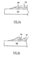
- Figure 3a diagrammatically shows an SOI on which a first stabox step was carried out.
- edges of the layers 101 and 102 form a steep bevel following polishing.
- this bevel shape in this case further exposes the intermediate layer 102; this exposure is even greater than in the case shown in Figure 1 .
- Figure 3b shows the same SOI, on which a polishing step and then a second stabox step were carried out after the first stabox step.
- the intermediate layer 102 is still exposed, and is therefore still subject to attack by subsequent treatments applied to the wafer.
- EP1158581 and WO 031005434 describes process for improving the roughness of a water
- the purpose of the invention is to overcome said disadvantages.
- the invention proposes a process for treatment of the ring of a multilayer wafer made by layer transfer and composed of materials chosen from among semiconducting materials, said wafer comprising at least an intermediate layer between a superficial region and a base layer this treatment of the ring consisting in preventing the attack on the peripheral part of said intermediate layer of the wafer during ,a subsequent treatment step of the wafer.
- the process includes rapid thermal annealing of the wafer to cause overlapping and encapsulation of the peripheral edge of said intermediate layer, by a layer of said superficial region of the surface of the wafer.
- wafers to which the invention is applicable may be SOI wafers.
- the starting point of the process according to the invention is a wafer that typically comprises a ring like that shown diagrammatically in Figure 1 .
- a rapid thermal annealing of the wafer is carried out on this type of wafer in order to overlap and then encapsulate the peripheral edge of the exposed intermediate layer, by a layer on a surface region of the wafer.
- RTA Rapid Thermal Annealing
- the RTA can make the surface layer of the wafer "drop off" (in fact layer 101 in Figure 1 that corresponds to a layer of monocrystalline silicon in the case of an SOI wafer).
- this surface layer also overlaps and encapsulates the periphery of the intermediate layer (layer 102 in Figure 1 ) that was previously exposed.
- Figure 4 illustrates the case of an SOI wafer on which an RTA was carried out after being exposed to a stabox step.
- the intermediate layer 102 is entirely encapsulated by the surface layer 101.
- the layer 102 is thus protected from subsequent heat treatments that may be applied to the wafer.
- the RTA is carried out at a high temperature for a short period.
- the treatment may be carried out at a temperature of the order of 1200°C for a period of less than 3 minutes.
- This RTA is carried out in a hydrogen and / or argon atmosphere.
- the RTA can also be done immediately after the wafer has been detached.
- the bonding interface between the layer 103 and the rest of the wafer was not stabilized by a heat treatment.
- FIG. 5 is an illustration of this embodiment of the invention.
- the RTA can thus be used immediately after the wafer has been detached, or during a subsequent step.
- the RTA can be done after a stabox step (see Figure 4 ).
- wafers concerned by this invention are not limited to SOI wafers.
- this layer may be the surface layer of the wafer, as shown in the examples illustrated and commented upon above.
- the RTA protects the intermediate layer of the wafer so that it is then possible to apply treatments like those mentioned at the beginning of the text, to this wafer.
- a wafer treated according to the invention can be subjected to a prolonged high temperature heat treatment, while this type of treatment would have degraded the intermediate layer if the invention is not used.
- a polishing step (possibly CMP) should not be done between the RTA according to the invention and the prolonged high temperature heat treatment.
- This polishing step would at least partially destroy the protection applied to the intermediate layer by the invention, such that the prolonged high temperature heat treatment could degrade the intermediate layer.
Landscapes
- Engineering & Computer Science (AREA)
- Physics & Mathematics (AREA)
- Condensed Matter Physics & Semiconductors (AREA)
- General Physics & Mathematics (AREA)
- Manufacturing & Machinery (AREA)
- Computer Hardware Design (AREA)
- Microelectronics & Electronic Packaging (AREA)
- Power Engineering (AREA)
- Element Separation (AREA)
- Recrystallisation Techniques (AREA)
- Mechanical Treatment Of Semiconductor (AREA)
Claims (10)
- Prozess zum Behandeln des Rings (110) eines Mehrschichtwafers (10), der durch Schichttransfer hergestellt ist und aus Materialien gebildet ist, die unter Halbleitermaterialien ausgewählt sind, wobei der Wafer mindestens eine Zwischenschicht (102) zwischen einer Oberflächenregion (101) und einer Basisschicht (103) umfasst, wobei dieses Behandeln des Rings (110) darin besteht, das Angreifen des peripheren Teils der Zwischenschicht (102) des Wafers (10) während eines anschließenden Behandlungsschrittes des Wafers zu verhindern, dadurch gekennzeichnet, dass der Prozess ein schnelles thermisches Glühen des Wafers (10) umfasst, um ein Überlappen und Verkapseln des peripheren Randes der Zwischenschicht (102) durch eine Schicht der Oberflächenregion (101) der Oberfläche des Wafers zu bewirken.
- Prozess nach Anspruch 1, dadurch gekennzeichnet, dass er einen Stabox-Schritt umfasst und dass das thermische Glühen nach dem Stabox-Schritt durchgeführt wird, wobei der Stabox-Schritt durch die folgende Sequenz von Arbeitsschritten definiert ist:- Oxidieren der Oberfläche des Wafers (10) - dieser Arbeitsschritt dient dazu, eine Oxidschicht auf der Oberfläche des Wafers (10) abzuscheiden, die diese Oberfläche während des nächsten Wärmebehandlungsschrittes schützt,- stabilisierende Wärmebehandlung einer Bondungsgrenzfläche - zum Beispiel durch Glühen bei einer Temperatur in der Größenordnung von 1.100°C,- Entoxidieren des auf der Oberfläche des Wafers (10) abgeschiedenen Oxids - zum Beispiel durch chemischen Angriff in einer HF-Ätzlösung mit einer HF-Lösung mit einer Konzentration von 10 bis 20 %.
- Prozess nach Anspruch 1, dadurch gekennzeichnet, dass das schnelle thermische Glühen unmittelbar nach dem Transfer des Wafers (10) durchgeführt wird.
- Prozess nach Anspruch 1, dadurch gekennzeichnet, dass das schnelle thermische Glühen nach einem zusätzlichen Behandlungsschritt zwischen dem Transfer des Wafers (10) und dem schnellen thermischen Glühen durchgeführt wird.
- Prozess nach einem der vorangehenden Ansprüche, dadurch gekennzeichnet, dass das schnelle thermische Glühen bei einer Temperatur in der Größenordnung von 1200 °C durchgeführt wird.
- Prozess nach einem der vorangehenden Ansprüche, dadurch gekennzeichnet, dass das schnelle thermische Glühen über eine Dauer von weniger als 3 Minuten durchgeführt wird.
- Prozess nach einem der vorangehenden Ansprüche, dadurch gekennzeichnet, dass das schnelle thermische Glühen unter einer Wasserstoff- und/oder Argonatmosphäre durchgeführt wird.
- Prozess nach einem der vorangehenden Ansprüche, dadurch gekennzeichnet, dass der Wafer (10) ein SOI ist.
- Prozess nach einem der vorangehenden Ansprüche, dadurch gekennzeichnet, dass der Transfer mittels eines SMARTCUT(R)-Prozesses durchgeführt wurde.
- Prozess nach einem der vorangehenden Ansprüche, dadurch gekennzeichnet, dass der anschließende Behandlungsschritt des Wafers (10) einen chemischen Angriff oder eine längere Hochtemperatur-Wärmebehandlung umfasst.
Applications Claiming Priority (3)
| Application Number | Priority Date | Filing Date | Title |
|---|---|---|---|
| FR0302623 | 2003-03-04 | ||
| FR0302623A FR2852143B1 (fr) | 2003-03-04 | 2003-03-04 | Procede de traitement preventif de la couronne d'une tranche multicouche |
| PCT/IB2004/000940 WO2004079801A1 (en) | 2003-03-04 | 2004-03-01 | Preventive treatment process for the ring of a multilayer wafer |
Publications (2)
| Publication Number | Publication Date |
|---|---|
| EP1599896A1 EP1599896A1 (de) | 2005-11-30 |
| EP1599896B1 true EP1599896B1 (de) | 2012-11-14 |
Family
ID=32865218
Family Applications (1)
| Application Number | Title | Priority Date | Filing Date |
|---|---|---|---|
| EP04715980A Expired - Lifetime EP1599896B1 (de) | 2003-03-04 | 2004-03-01 | Verfahren zur präventiven Behandlung des Ringes eines mehrschichtigen Wafers |
Country Status (8)
| Country | Link |
|---|---|
| US (2) | US6939783B2 (de) |
| EP (1) | EP1599896B1 (de) |
| JP (1) | JP4855245B2 (de) |
| KR (1) | KR100806981B1 (de) |
| CN (1) | CN100490070C (de) |
| FR (1) | FR2852143B1 (de) |
| TW (1) | TWI297176B (de) |
| WO (1) | WO2004079801A1 (de) |
Families Citing this family (11)
| Publication number | Priority date | Publication date | Assignee | Title |
|---|---|---|---|---|
| US7579044B2 (en) * | 2004-11-08 | 2009-08-25 | Brewer Science Inc. | Process and device for coating the outer edge of a substrate during microelectronics manufacture |
| JP2008526010A (ja) | 2004-12-28 | 2008-07-17 | エス. オー. アイ. テック シリコン オン インシュレーター テクノロジーズ | 低いホール密度を有する薄層を得るための方法 |
| FR2880988B1 (fr) | 2005-01-19 | 2007-03-30 | Soitec Silicon On Insulator | TRAITEMENT D'UNE COUCHE EN SI1-yGEy PRELEVEE |
| FR2895563B1 (fr) | 2005-12-22 | 2008-04-04 | Soitec Silicon On Insulator | Procede de simplification d'une sequence de finition et structure obtenue par le procede |
| FR2941324B1 (fr) * | 2009-01-22 | 2011-04-29 | Soitec Silicon On Insulator | Procede de dissolution de la couche d'oxyde dans la couronne d'une structure de type semi-conducteur sur isolant. |
| US7927975B2 (en) | 2009-02-04 | 2011-04-19 | Micron Technology, Inc. | Semiconductor material manufacture |
| FR2943458B1 (fr) | 2009-03-18 | 2011-06-10 | Soitec Silicon On Insulator | Procede de finition d'un substrat de type "silicium sur isolant" soi |
| FR2944645B1 (fr) * | 2009-04-21 | 2011-09-16 | Soitec Silicon On Insulator | Procede d'amincissement d'un substrat silicium sur isolant |
| KR101057192B1 (ko) * | 2009-04-30 | 2011-08-16 | 주식회사 하이닉스반도체 | 노광 과정으로 웨이퍼 상에 패턴을 형성하는 방법 |
| FR2957716B1 (fr) * | 2010-03-18 | 2012-10-05 | Soitec Silicon On Insulator | Procede de finition d'un substrat de type semi-conducteur sur isolant |
| FR3003997B1 (fr) * | 2013-03-29 | 2015-03-20 | Soitec Silicon On Insulator | Procede de fabrication d'une structure composite |
Family Cites Families (20)
| Publication number | Priority date | Publication date | Assignee | Title |
|---|---|---|---|---|
| US5086011A (en) * | 1987-01-27 | 1992-02-04 | Advanced Micro Devices, Inc. | Process for producing thin single crystal silicon islands on insulator |
| US4795718A (en) * | 1987-05-12 | 1989-01-03 | Harris Corporation | Self-aligned contact for MOS processing |
| FR2629636B1 (fr) * | 1988-04-05 | 1990-11-16 | Thomson Csf | Procede de realisation d'une alternance de couches de materiau semiconducteur monocristallin et de couches de materiau isolant |
| JP2645478B2 (ja) * | 1988-10-07 | 1997-08-25 | 富士通株式会社 | 半導体装置の製造方法 |
| JPH04129267A (ja) * | 1990-09-20 | 1992-04-30 | Fujitsu Ltd | 半導体基板およびその製造方法 |
| US5091330A (en) * | 1990-12-28 | 1992-02-25 | Motorola, Inc. | Method of fabricating a dielectric isolated area |
| JPH07161948A (ja) * | 1993-12-10 | 1995-06-23 | Canon Inc | 半導体基体及びその製造方法 |
| US5723385A (en) * | 1996-12-16 | 1998-03-03 | Taiwan Semiconductor Manufacturing Company, Ltd | Wafer edge seal ring structure |
| JP3875375B2 (ja) * | 1997-10-06 | 2007-01-31 | 株式会社ルネサステクノロジ | 半導体装置の製造方法および半導体基板 |
| JP3846657B2 (ja) * | 1997-11-28 | 2006-11-15 | 株式会社Sumco | 貼り合わせ基板およびその製造方法 |
| JPH11204452A (ja) * | 1998-01-13 | 1999-07-30 | Mitsubishi Electric Corp | 半導体基板の処理方法および半導体基板 |
| JP3887973B2 (ja) * | 1998-10-16 | 2007-02-28 | 信越半導体株式会社 | Soiウエーハの製造方法及びsoiウエーハ |
| JP2000299451A (ja) * | 1999-04-15 | 2000-10-24 | Matsushita Electric Works Ltd | Soiウェハおよびその製造方法 |
| FR2797714B1 (fr) | 1999-08-20 | 2001-10-26 | Soitec Silicon On Insulator | Procede de traitement de substrats pour la microelectronique et substrats obtenus par ce procede |
| KR100730806B1 (ko) * | 1999-10-14 | 2007-06-20 | 신에쯔 한도타이 가부시키가이샤 | Soi웨이퍼의 제조방법 및 soi 웨이퍼 |
| DE60029578T2 (de) * | 1999-10-14 | 2007-07-26 | Shin-Etsu Handotai Co., Ltd. | Verbundscheiben-herstellungsmethode |
| JP2002299451A (ja) * | 2001-03-30 | 2002-10-11 | Toshiba Corp | 半導体装置 |
| FR2827078B1 (fr) * | 2001-07-04 | 2005-02-04 | Soitec Silicon On Insulator | Procede de diminution de rugosite de surface |
| JP2003224247A (ja) * | 2002-01-29 | 2003-08-08 | Shin Etsu Handotai Co Ltd | Soiウエーハ及びsoiウエーハの製造方法 |
| JP2003309253A (ja) * | 2002-02-18 | 2003-10-31 | Shin Etsu Handotai Co Ltd | Soiウエーハ及びsoiウエーハの製造方法 |
-
2003
- 2003-03-04 FR FR0302623A patent/FR2852143B1/fr not_active Expired - Lifetime
-
2004
- 2004-02-20 US US10/784,040 patent/US6939783B2/en not_active Expired - Lifetime
- 2004-03-01 JP JP2006506406A patent/JP4855245B2/ja not_active Expired - Lifetime
- 2004-03-01 WO PCT/IB2004/000940 patent/WO2004079801A1/en not_active Ceased
- 2004-03-01 CN CNB2004800059654A patent/CN100490070C/zh not_active Expired - Lifetime
- 2004-03-01 KR KR1020057016240A patent/KR100806981B1/ko not_active Expired - Lifetime
- 2004-03-01 EP EP04715980A patent/EP1599896B1/de not_active Expired - Lifetime
- 2004-03-03 TW TW093105459A patent/TWI297176B/zh not_active IP Right Cessation
-
2005
- 2005-06-22 US US11/157,956 patent/US7190029B2/en not_active Expired - Lifetime
Also Published As
| Publication number | Publication date |
|---|---|
| US20040197963A1 (en) | 2004-10-07 |
| TWI297176B (en) | 2008-05-21 |
| KR20050109521A (ko) | 2005-11-21 |
| CN100490070C (zh) | 2009-05-20 |
| JP2006519504A (ja) | 2006-08-24 |
| WO2004079801A1 (en) | 2004-09-16 |
| FR2852143B1 (fr) | 2005-10-14 |
| US20050230754A1 (en) | 2005-10-20 |
| JP4855245B2 (ja) | 2012-01-18 |
| CN1757097A (zh) | 2006-04-05 |
| FR2852143A1 (fr) | 2004-09-10 |
| TW200501236A (en) | 2005-01-01 |
| US7190029B2 (en) | 2007-03-13 |
| US6939783B2 (en) | 2005-09-06 |
| KR100806981B1 (ko) | 2008-02-25 |
| WO2004079801A8 (en) | 2005-04-07 |
| EP1599896A1 (de) | 2005-11-30 |
Similar Documents
| Publication | Publication Date | Title |
|---|---|---|
| US7902038B2 (en) | Detachable substrate with controlled mechanical strength and method of producing same | |
| JP3943782B2 (ja) | 剥離ウエーハの再生処理方法及び再生処理された剥離ウエーハ | |
| US8951887B2 (en) | Process for fabricating a semiconductor structure employing a temporary bond | |
| CN102396051B (zh) | 使绝缘体上硅衬底减薄的方法 | |
| US20050029224A1 (en) | Detachable substrate or detachable structure and method for the production thereof | |
| US9136113B2 (en) | Process to dissolve the oxide layer in the peripheral ring of a structure of semiconductor-on-insulator type | |
| JP5926527B2 (ja) | 透明soiウェーハの製造方法 | |
| EP1599896B1 (de) | Verfahren zur präventiven Behandlung des Ringes eines mehrschichtigen Wafers | |
| US7572714B2 (en) | Film taking-off method | |
| CN1959952B (zh) | 再循环外延施予晶片的方法 | |
| JP2011515838A (ja) | セミコンダクタオンインシュレータ型基板を製作する方法 | |
| JP5025957B2 (ja) | 欠陥クラスタを有する基板内に形成された薄い層を転写する方法 | |
| JP2003224247A (ja) | Soiウエーハ及びsoiウエーハの製造方法 | |
| JP4926077B2 (ja) | 溶融層を用いた歪み層の歪み緩和 | |
| JP5125194B2 (ja) | 貼り合わせウエーハの製造方法 | |
| JP5531642B2 (ja) | 貼り合わせウェーハの製造方法 | |
| JP4844356B2 (ja) | 半導体装置の製造方法 |
Legal Events
| Date | Code | Title | Description |
|---|---|---|---|
| PUAI | Public reference made under article 153(3) epc to a published international application that has entered the european phase |
Free format text: ORIGINAL CODE: 0009012 |
|
| 17P | Request for examination filed |
Effective date: 20050928 |
|
| AK | Designated contracting states |
Kind code of ref document: A1 Designated state(s): AT BE BG CH CY CZ DE DK EE ES FI FR GB GR HU IE IT LI LU MC NL PL PT RO SE SI SK TR |
|
| AX | Request for extension of the european patent |
Extension state: AL LT LV MK |
|
| DAX | Request for extension of the european patent (deleted) | ||
| 17Q | First examination report despatched |
Effective date: 20100422 |
|
| RAP1 | Party data changed (applicant data changed or rights of an application transferred) |
Owner name: SOITEC |
|
| GRAP | Despatch of communication of intention to grant a patent |
Free format text: ORIGINAL CODE: EPIDOSNIGR1 |
|
| GRAS | Grant fee paid |
Free format text: ORIGINAL CODE: EPIDOSNIGR3 |
|
| GRAA | (expected) grant |
Free format text: ORIGINAL CODE: 0009210 |
|
| AK | Designated contracting states |
Kind code of ref document: B1 Designated state(s): AT BE BG CH CY CZ DE DK EE ES FI FR GB GR HU IE IT LI LU MC NL PL PT RO SE SI SK TR |
|
| REG | Reference to a national code |
Ref country code: GB Ref legal event code: FG4D |
|
| RIN1 | Information on inventor provided before grant (corrected) |
Inventor name: MALLEVILLE, CHRISTOPHE Inventor name: NEYRET, ERIC |
|
| REG | Reference to a national code |
Ref country code: CH Ref legal event code: EP Ref country code: AT Ref legal event code: REF Ref document number: 584366 Country of ref document: AT Kind code of ref document: T Effective date: 20121115 |
|
| REG | Reference to a national code |
Ref country code: IE Ref legal event code: FG4D |
|
| REG | Reference to a national code |
Ref country code: DE Ref legal event code: R096 Ref document number: 602004040030 Country of ref document: DE Effective date: 20130110 |
|
| REG | Reference to a national code |
Ref country code: NL Ref legal event code: T3 |
|
| REG | Reference to a national code |
Ref country code: AT Ref legal event code: MK05 Ref document number: 584366 Country of ref document: AT Kind code of ref document: T Effective date: 20121114 |
|
| PG25 | Lapsed in a contracting state [announced via postgrant information from national office to epo] |
Ref country code: FI Free format text: LAPSE BECAUSE OF FAILURE TO SUBMIT A TRANSLATION OF THE DESCRIPTION OR TO PAY THE FEE WITHIN THE PRESCRIBED TIME-LIMIT Effective date: 20121114 Ref country code: ES Free format text: LAPSE BECAUSE OF FAILURE TO SUBMIT A TRANSLATION OF THE DESCRIPTION OR TO PAY THE FEE WITHIN THE PRESCRIBED TIME-LIMIT Effective date: 20130225 Ref country code: SE Free format text: LAPSE BECAUSE OF FAILURE TO SUBMIT A TRANSLATION OF THE DESCRIPTION OR TO PAY THE FEE WITHIN THE PRESCRIBED TIME-LIMIT Effective date: 20121114 |
|
| PG25 | Lapsed in a contracting state [announced via postgrant information from national office to epo] |
Ref country code: PL Free format text: LAPSE BECAUSE OF FAILURE TO SUBMIT A TRANSLATION OF THE DESCRIPTION OR TO PAY THE FEE WITHIN THE PRESCRIBED TIME-LIMIT Effective date: 20121114 Ref country code: CY Free format text: LAPSE BECAUSE OF FAILURE TO SUBMIT A TRANSLATION OF THE DESCRIPTION OR TO PAY THE FEE WITHIN THE PRESCRIBED TIME-LIMIT Effective date: 20121114 Ref country code: PT Free format text: LAPSE BECAUSE OF FAILURE TO SUBMIT A TRANSLATION OF THE DESCRIPTION OR TO PAY THE FEE WITHIN THE PRESCRIBED TIME-LIMIT Effective date: 20130314 Ref country code: BE Free format text: LAPSE BECAUSE OF FAILURE TO SUBMIT A TRANSLATION OF THE DESCRIPTION OR TO PAY THE FEE WITHIN THE PRESCRIBED TIME-LIMIT Effective date: 20121114 Ref country code: GR Free format text: LAPSE BECAUSE OF FAILURE TO SUBMIT A TRANSLATION OF THE DESCRIPTION OR TO PAY THE FEE WITHIN THE PRESCRIBED TIME-LIMIT Effective date: 20130215 Ref country code: SI Free format text: LAPSE BECAUSE OF FAILURE TO SUBMIT A TRANSLATION OF THE DESCRIPTION OR TO PAY THE FEE WITHIN THE PRESCRIBED TIME-LIMIT Effective date: 20121114 |
|
| PG25 | Lapsed in a contracting state [announced via postgrant information from national office to epo] |
Ref country code: AT Free format text: LAPSE BECAUSE OF FAILURE TO SUBMIT A TRANSLATION OF THE DESCRIPTION OR TO PAY THE FEE WITHIN THE PRESCRIBED TIME-LIMIT Effective date: 20121114 |
|
| PG25 | Lapsed in a contracting state [announced via postgrant information from national office to epo] |
Ref country code: SK Free format text: LAPSE BECAUSE OF FAILURE TO SUBMIT A TRANSLATION OF THE DESCRIPTION OR TO PAY THE FEE WITHIN THE PRESCRIBED TIME-LIMIT Effective date: 20121114 Ref country code: CZ Free format text: LAPSE BECAUSE OF FAILURE TO SUBMIT A TRANSLATION OF THE DESCRIPTION OR TO PAY THE FEE WITHIN THE PRESCRIBED TIME-LIMIT Effective date: 20121114 Ref country code: DK Free format text: LAPSE BECAUSE OF FAILURE TO SUBMIT A TRANSLATION OF THE DESCRIPTION OR TO PAY THE FEE WITHIN THE PRESCRIBED TIME-LIMIT Effective date: 20121114 Ref country code: EE Free format text: LAPSE BECAUSE OF FAILURE TO SUBMIT A TRANSLATION OF THE DESCRIPTION OR TO PAY THE FEE WITHIN THE PRESCRIBED TIME-LIMIT Effective date: 20121114 Ref country code: BG Free format text: LAPSE BECAUSE OF FAILURE TO SUBMIT A TRANSLATION OF THE DESCRIPTION OR TO PAY THE FEE WITHIN THE PRESCRIBED TIME-LIMIT Effective date: 20130214 |
|
| PG25 | Lapsed in a contracting state [announced via postgrant information from national office to epo] |
Ref country code: RO Free format text: LAPSE BECAUSE OF FAILURE TO SUBMIT A TRANSLATION OF THE DESCRIPTION OR TO PAY THE FEE WITHIN THE PRESCRIBED TIME-LIMIT Effective date: 20121114 |
|
| PLBE | No opposition filed within time limit |
Free format text: ORIGINAL CODE: 0009261 |
|
| STAA | Information on the status of an ep patent application or granted ep patent |
Free format text: STATUS: NO OPPOSITION FILED WITHIN TIME LIMIT |
|
| 26N | No opposition filed |
Effective date: 20130815 |
|
| PG25 | Lapsed in a contracting state [announced via postgrant information from national office to epo] |
Ref country code: MC Free format text: LAPSE BECAUSE OF NON-PAYMENT OF DUE FEES Effective date: 20130331 |
|
| REG | Reference to a national code |
Ref country code: CH Ref legal event code: PL |
|
| REG | Reference to a national code |
Ref country code: DE Ref legal event code: R097 Ref document number: 602004040030 Country of ref document: DE Effective date: 20130815 |
|
| REG | Reference to a national code |
Ref country code: IE Ref legal event code: MM4A |
|
| PG25 | Lapsed in a contracting state [announced via postgrant information from national office to epo] |
Ref country code: IE Free format text: LAPSE BECAUSE OF NON-PAYMENT OF DUE FEES Effective date: 20130301 Ref country code: CH Free format text: LAPSE BECAUSE OF NON-PAYMENT OF DUE FEES Effective date: 20130331 Ref country code: LI Free format text: LAPSE BECAUSE OF NON-PAYMENT OF DUE FEES Effective date: 20130331 |
|
| PG25 | Lapsed in a contracting state [announced via postgrant information from national office to epo] |
Ref country code: TR Free format text: LAPSE BECAUSE OF FAILURE TO SUBMIT A TRANSLATION OF THE DESCRIPTION OR TO PAY THE FEE WITHIN THE PRESCRIBED TIME-LIMIT Effective date: 20121114 |
|
| REG | Reference to a national code |
Ref country code: DE Ref legal event code: R082 Ref document number: 602004040030 Country of ref document: DE Representative=s name: HOEGER, STELLRECHT & PARTNER PATENTANWAELTE MB, DE |
|
| PG25 | Lapsed in a contracting state [announced via postgrant information from national office to epo] |
Ref country code: LU Free format text: LAPSE BECAUSE OF NON-PAYMENT OF DUE FEES Effective date: 20130301 Ref country code: HU Free format text: LAPSE BECAUSE OF FAILURE TO SUBMIT A TRANSLATION OF THE DESCRIPTION OR TO PAY THE FEE WITHIN THE PRESCRIBED TIME-LIMIT; INVALID AB INITIO Effective date: 20040301 |
|
| REG | Reference to a national code |
Ref country code: FR Ref legal event code: PLFP Year of fee payment: 13 |
|
| REG | Reference to a national code |
Ref country code: FR Ref legal event code: PLFP Year of fee payment: 14 |
|
| REG | Reference to a national code |
Ref country code: FR Ref legal event code: PLFP Year of fee payment: 15 |
|
| REG | Reference to a national code |
Ref country code: DE Ref legal event code: R082 Ref document number: 602004040030 Country of ref document: DE Representative=s name: HOEGER, STELLRECHT & PARTNER PATENTANWAELTE MB, DE |
|
| PGFP | Annual fee paid to national office [announced via postgrant information from national office to epo] |
Ref country code: NL Payment date: 20230215 Year of fee payment: 20 |
|
| PGFP | Annual fee paid to national office [announced via postgrant information from national office to epo] |
Ref country code: FR Payment date: 20230221 Year of fee payment: 20 |
|
| PGFP | Annual fee paid to national office [announced via postgrant information from national office to epo] |
Ref country code: IT Payment date: 20230213 Year of fee payment: 20 Ref country code: GB Payment date: 20230202 Year of fee payment: 20 Ref country code: DE Payment date: 20230131 Year of fee payment: 20 |
|
| REG | Reference to a national code |
Ref country code: DE Ref legal event code: R071 Ref document number: 602004040030 Country of ref document: DE |
|
| REG | Reference to a national code |
Ref country code: NL Ref legal event code: MK Effective date: 20240229 |
|
| REG | Reference to a national code |
Ref country code: GB Ref legal event code: PE20 Expiry date: 20240229 |
|
| PG25 | Lapsed in a contracting state [announced via postgrant information from national office to epo] |
Ref country code: GB Free format text: LAPSE BECAUSE OF EXPIRATION OF PROTECTION Effective date: 20240229 |