EP1580813A2 - Halbleitersubstrat, Halbleiterbauelement und zugehörige Herstellungsverfahren - Google Patents
Halbleitersubstrat, Halbleiterbauelement und zugehörige Herstellungsverfahren Download PDFInfo
- Publication number
- EP1580813A2 EP1580813A2 EP05251798A EP05251798A EP1580813A2 EP 1580813 A2 EP1580813 A2 EP 1580813A2 EP 05251798 A EP05251798 A EP 05251798A EP 05251798 A EP05251798 A EP 05251798A EP 1580813 A2 EP1580813 A2 EP 1580813A2
- Authority
- EP
- European Patent Office
- Prior art keywords
- substrate
- insulating film
- monocrystalline
- semiconductor
- singlecrystalline
- Prior art date
- Legal status (The legal status is an assumption and is not a legal conclusion. Google has not performed a legal analysis and makes no representation as to the accuracy of the status listed.)
- Withdrawn
Links
Images


Classifications
-
- H—ELECTRICITY
- H10—SEMICONDUCTOR DEVICES; ELECTRIC SOLID-STATE DEVICES NOT OTHERWISE PROVIDED FOR
- H10D—INORGANIC ELECTRIC SEMICONDUCTOR DEVICES
- H10D86/00—Integrated devices formed in or on insulating or conducting substrates, e.g. formed in silicon-on-insulator [SOI] substrates or on stainless steel or glass substrates
- H10D86/01—Manufacture or treatment
- H10D86/021—Manufacture or treatment of multiple TFTs
- H10D86/0214—Manufacture or treatment of multiple TFTs using temporary substrates
-
- H—ELECTRICITY
- H10—SEMICONDUCTOR DEVICES; ELECTRIC SOLID-STATE DEVICES NOT OTHERWISE PROVIDED FOR
- H10P—GENERIC PROCESSES OR APPARATUS FOR THE MANUFACTURE OR TREATMENT OF DEVICES COVERED BY CLASS H10
- H10P10/00—Bonding of wafers, substrates or parts of devices
-
- H—ELECTRICITY
- H10—SEMICONDUCTOR DEVICES; ELECTRIC SOLID-STATE DEVICES NOT OTHERWISE PROVIDED FOR
- H10D—INORGANIC ELECTRIC SEMICONDUCTOR DEVICES
- H10D30/00—Field-effect transistors [FET]
- H10D30/60—Insulated-gate field-effect transistors [IGFET]
- H10D30/67—Thin-film transistors [TFT]
- H10D30/6704—Thin-film transistors [TFT] having supplementary regions or layers in the thin films or in the insulated bulk substrates for controlling properties of the device
- H10D30/6706—Thin-film transistors [TFT] having supplementary regions or layers in the thin films or in the insulated bulk substrates for controlling properties of the device for preventing leakage current
-
- H—ELECTRICITY
- H10—SEMICONDUCTOR DEVICES; ELECTRIC SOLID-STATE DEVICES NOT OTHERWISE PROVIDED FOR
- H10D—INORGANIC ELECTRIC SEMICONDUCTOR DEVICES
- H10D30/00—Field-effect transistors [FET]
- H10D30/60—Insulated-gate field-effect transistors [IGFET]
- H10D30/67—Thin-film transistors [TFT]
- H10D30/6758—Thin-film transistors [TFT] characterised by the insulating substrates
-
- H—ELECTRICITY
- H10—SEMICONDUCTOR DEVICES; ELECTRIC SOLID-STATE DEVICES NOT OTHERWISE PROVIDED FOR
- H10D—INORGANIC ELECTRIC SEMICONDUCTOR DEVICES
- H10D86/00—Integrated devices formed in or on insulating or conducting substrates, e.g. formed in silicon-on-insulator [SOI] substrates or on stainless steel or glass substrates
- H10D86/201—Integrated devices formed in or on insulating or conducting substrates, e.g. formed in silicon-on-insulator [SOI] substrates or on stainless steel or glass substrates the substrates comprising an insulating layer on a semiconductor body, e.g. SOI
-
- H—ELECTRICITY
- H10—SEMICONDUCTOR DEVICES; ELECTRIC SOLID-STATE DEVICES NOT OTHERWISE PROVIDED FOR
- H10D—INORGANIC ELECTRIC SEMICONDUCTOR DEVICES
- H10D86/00—Integrated devices formed in or on insulating or conducting substrates, e.g. formed in silicon-on-insulator [SOI] substrates or on stainless steel or glass substrates
- H10D86/40—Integrated devices formed in or on insulating or conducting substrates, e.g. formed in silicon-on-insulator [SOI] substrates or on stainless steel or glass substrates characterised by multiple TFTs
- H10D86/60—Integrated devices formed in or on insulating or conducting substrates, e.g. formed in silicon-on-insulator [SOI] substrates or on stainless steel or glass substrates characterised by multiple TFTs wherein the TFTs are in active matrices
-
- H—ELECTRICITY
- H10—SEMICONDUCTOR DEVICES; ELECTRIC SOLID-STATE DEVICES NOT OTHERWISE PROVIDED FOR
- H10P—GENERIC PROCESSES OR APPARATUS FOR THE MANUFACTURE OR TREATMENT OF DEVICES COVERED BY CLASS H10
- H10P90/00—Preparation of wafers not covered by a single main group of this subclass, e.g. wafer reinforcement
- H10P90/19—Preparing inhomogeneous wafers
- H10P90/1904—Preparing vertically inhomogeneous wafers
- H10P90/1906—Preparing SOI wafers
- H10P90/1914—Preparing SOI wafers using bonding
- H10P90/1916—Preparing SOI wafers using bonding with separation or delamination along an ion implanted layer, e.g. Smart-cut
-
- H—ELECTRICITY
- H10—SEMICONDUCTOR DEVICES; ELECTRIC SOLID-STATE DEVICES NOT OTHERWISE PROVIDED FOR
- H10W—GENERIC PACKAGES, INTERCONNECTIONS, CONNECTORS OR OTHER CONSTRUCTIONAL DETAILS OF DEVICES COVERED BY CLASS H10
- H10W10/00—Isolation regions in semiconductor bodies between components of integrated devices
- H10W10/01—Manufacture or treatment
- H10W10/011—Manufacture or treatment of isolation regions comprising dielectric materials
- H10W10/012—Manufacture or treatment of isolation regions comprising dielectric materials using local oxidation of silicon [LOCOS]
-
- H—ELECTRICITY
- H10—SEMICONDUCTOR DEVICES; ELECTRIC SOLID-STATE DEVICES NOT OTHERWISE PROVIDED FOR
- H10W—GENERIC PACKAGES, INTERCONNECTIONS, CONNECTORS OR OTHER CONSTRUCTIONAL DETAILS OF DEVICES COVERED BY CLASS H10
- H10W10/00—Isolation regions in semiconductor bodies between components of integrated devices
- H10W10/10—Isolation regions comprising dielectric materials
- H10W10/13—Isolation regions comprising dielectric materials formed using local oxidation of silicon [LOCOS], e.g. sealed interface localised oxidation [SILO] or side-wall mask isolation [SWAMI]
-
- H—ELECTRICITY
- H10—SEMICONDUCTOR DEVICES; ELECTRIC SOLID-STATE DEVICES NOT OTHERWISE PROVIDED FOR
- H10W—GENERIC PACKAGES, INTERCONNECTIONS, CONNECTORS OR OTHER CONSTRUCTIONAL DETAILS OF DEVICES COVERED BY CLASS H10
- H10W10/00—Isolation regions in semiconductor bodies between components of integrated devices
- H10W10/10—Isolation regions comprising dielectric materials
- H10W10/181—Semiconductor-on-insulator [SOI] isolation regions, e.g. buried oxide regions of SOI wafers
Definitions
- the present invention relates to a semiconductor substrate and a semiconductor device used for an active matrix liquid crystal display device that is driven by TFTs (Thin Film transistor), such as a high-functional liquid crystal display device, an OLED (Organic Light Emitting Diode: Organic EL) display device or the like, in which the peripheral circuits, the control circuit, the MPU (Micro Processing Unit), and/or the image processing circuit are all integrated into a single substrate.
- TFTs Thin Film transistor
- OLED Organic Light Emitting Diode: Organic EL
- the present invention also provides fabrication method for the semiconductor substrate/ device.
- the present invention particularly relates to a system-on-panel technology that offers great improvement of circuit performance with the use of singlecrystalline thin film device, the fabrication method thereof, a device structure for making the semiconductor device using the technology, and a fabrication method for realizing coexistence of a singlecrystalline device and a non-singlecrystalline device, a polycrystalline Si in particular.
- the present invention enables formation of two types of semiconductor device with different characteristics, allowing efficient use of respective benefits of those devices, thereby the resulting product is applicable not only to a display device but also to other various purposes.
- the present invention is particularly applicable to a semiconductor substrate and a semiconductor device used for an active matrix liquid crystal display device driven by TFTs (Thin Film transistor), such as a high-functional liquid crystal display device or an OLED (Organic Light Emitting Diode: Organic EL) display device, in which the peripheral circuits, the control circuit, or the MPU (Micro Processing Unit), and/or the image processing circuit are all integrated into a single substrate.
- TFTs Thin Film transistor
- OLED Organic Light Emitting Diode: Organic EL
- a display device driven by so-called an active matrix manner has come into practical use, and the production amount is increasing.
- a liquid crystal display panel or an organic EL panel is driven with a Thin Film Transistor (hereinafter referred to as a TFT), which is made of an amorphous Si (hereinafter referred to as an a-Si) or a polycrystalline Si (hereinafter referred to as a Poly-Si), and is formed on the glass substrate as a switching element of the pixel.
- a TFT Thin Film Transistor
- a driver IC including a transistor made of a non-singlecrystalline Si, particularly a poly-Si, because of the variation in characteristics due to the particular crystal grain boundaries of poly-Si and poor quality of gate insulating film, thereby disabling the transistor to be adopted for integration of a complex system.
- display quality uniformity
- a general LSI includes MOS (Metal Oxide semiconductor) transistors formed from bulk singlecrystalline Si
- MOS Metal Oxide semiconductor
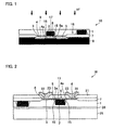
- the individual transistor needs to be driven separately to ensure adequate operation. Therefore, to separate the transistors into individual pieces (device isolation), or to prevent latch-up by a parasitic bipolar transistor, ion implantation, such as channel stop implantation section 101 or multiple well 102, is performed as shown in Figure 13.
- ion implantation such as channel stop implantation section 101 or multiple well 102
- the trend of miniaturization of transistor arises a new problem regarding the area for device isolation.
- retrograde well (reverse-impurity concentration gradient-well) structure or the like has been introduced; however, this structure requires ion implantation many times and makes the process complicated, thus causing a cost rise and a decrease in yield. Further, requirement of processes for forming bumps etc. increases time for fabrication, thereby decreasing the yield.
- the driver IC needs to be assembled onto a completed panel. This arises various problems, such as less-flexible and complicated manufacturing, low efficiency in distribution and manufacturing, and a cost rise which causes a decrease in yield.
- a device made of a singlecrystalline Si is formed on a bulk Si substrate, and is bonded to a glass substrate to create a display panel, and the insulator is then separated from the device layer through some kind of exfoliation.
- SOI Silicon On Insulator
- a possible method of performing the device transfer is removing an oxide film under the singlecrystalline Si from the SOI structure by etching so as to create a thin film device (Kopin Co. Ltd.) This method are described in detail, for example in Japanese Laid-Open Patent Application Tokuhyohei 07-503557 (published on April 13, 1995), and the following Documents 1 and 2.
- Tokuhyohei 07-503557 discloses a method of manufacturing a display panel for an active matrix-type liquid crystal display device, using a semiconductor device on which a singlecrystalline Si thin film transistor is transferred, the transfer is formed on a glass substrate in advance with an adhesive.
- Tokukaihei 10-125880 discloses a method of first creating level differences in the singlecrystalline Si, forming a small polishing stopper whose polishing rate is smaller than the singlecrystalline Si, then transferring the Si onto another Si substrate, and polishing the divided surface. By thus forming the stopper in a concave section of the step and using the difference in polishing speed, this method makes an island-shaped singlecrystalline Si thin film.
- the devices are formed on a silicon wafer, the total size of all devices to be provided thereon needs to fall within the silicon (Si) wafer.
- the size of silicon (Si) wafer is limited, and may be smaller than a large glass substrate in some cases.
- this method is more complicated as it first forms an operation region on a solid phase epitaxial film, which is a singlecrystalline layer of a thin film grown on a silicon dioxide (SiO 2 ), to make a singlecrystalline Si device, and then the silicon dioxide (SiO 2 ) is divided by etching. Therefore, this method suffers from a decrease in yield (transfer process, division/retention of thin film, epitaxial growth).
- An object of the present invention is to provide a semiconductor substrate and a semiconductor device for realizing a semiconductor device having a high-performance integrated system in which a non-singlecrystalline Si semiconductor element and a singlecrystalline Si semiconductor element are formed on a large insulating substrate.
- the semiconductor substrate/device of the present invention uses a simple method for forming the singlecrystalline Si portion, and ensures device isolation of a minute singlecrystalline Si semiconductor element without highly-accurate photolithography, when the semiconductor substrate is transferred onto a large insulating substrate.
- the present invention also provides fabrication methods of the semiconductor substrate/device.
- the semiconductor substrate according to the present invention comprises: a singlecrystalline Si substrate which includes an active layer having a channel region, a source region, and a drain region, the singlecrystalline Si substrate including at least a part of a device structure not containing a well-structure or a channel stop region; a gate insulating film formed on the singlecrystalline Si substrate; a gate electrode formed on the gate insulating film; a LOCOS oxide film whose thickness is more than a thickness of the gate insulating film, the LOCOS oxide film being formed on the singlecrystalline Si substrate by surrounding the active layer; and an insulating film formed over the gate electrode and the LOCOS oxide film.
- a fabrication method of a semiconductor substrate comprises the steps of: (i) forming a LOCOS oxide film outside a device area of a singlecrystalline Si substrate; (ii) forming a gate insulating film in the device area of the singlecrystalline Si substrate; (iii) selectively implanting impurity into the device area of the singlecrystalline Si substrate so as to form a source region, a drain region and a channel region which together constitute an active layer; (iv) forming an insulating film with a flat upper surface over the gate electrode, the gate insulating film, and the LOCOS oxide film; and (v) implanting through the insulating film one or plural kinds of ion selected from a hydrogen ion group or an inactive element ion group so as to form an ion implantation layer with a predetermined depth in the singlecrystallinc Si substrate.
- a fabrication method of a semiconductor substrate comprises the steps of: (i) forming a LOCOS oxide film outside a device area of a singlecrystalline Si substrate; (ii) forming a gate insulating film in the device area of the singlecrystalline Si substrate; (iii) selectively implanting impurity into the device area of the singlecrystalline Si substrate so as to form a source region, a drain region and a channel region which together constitute an active layer; (iv) forming a first insulating film with a flat upper surface over the gate electrode, the gate insulating film, and the LOCOS oxide film; (v) implanting through the first insulating film one or plural kinds of ion selected from a hydrogen ion group or an inactive element ion group so as to form an ion implantation layer with a predetermined depth in the singlecrystalline Si substrate; (vi) forming at least one first wiring layer above the first insulating film; and (vii) forming a
- an active layer having a channel region, a source region, and a drain region; and the singlecrystalline Si substrate includes at least a part of a device structure not containing a well-structure or a channel stop region.
- the resulting semiconductor device is superior in performance and less varied in characteristic.
- the area of the device area is reduced, allowing more dense integration, thereby realizing a highly-dense semiconductor substrate.
- the conventional well is omitted, the device may be made thinner than the conventional structure using a well.
- the semiconductor element can be made as a thin film which can coexist with the TFTs formed from other polycrystalline Si upon formation of the semiconductor device, allowing conduction between the semiconductor element and TFTs through common thin film wiring.
- the element can be isolated by etching back the Si thin film, which is created as a result of the cleavage, it is possible to ensure the device isolation of the minute singlecrystalline Si device even on the insulating substrate 25, such as a large glass substrate, without highly-accurate photolithography. Further, since the well is omitted, the fabrication process is simplified.
- the LOCOS oxide film thicker than the gate insulating film, is formed by surrounding the active layer. This LOCOS oxide film securely ensures the device isolation.
- the process for making the singlecrystalline Si is simplified. Further, the foregoing arrangement provides a semiconductor substrate and a fabrication method thereof, which ensures device isolation of the minute singlecrystalline Si semiconductor element without highly-accurate photolithography, when the singlecrystalline Si semiconductor element is transferred onto the large insulating substrate.
- a semiconductor device includes an insulating substrate, and a singlecrystalline Si semiconductor element formed on the insulating substrate, the singlecrystalline Si semiconductor element comprising: a gate electrode formed above the insulating substrate; a gate insulating film formed on the gate electrode; an active layer, which is formed on the gate insulating film and is made of a singlecrystalline Si layer having a channel region, a source region, and a drain region; a LOCOS oxide film formed around the active layer; and an interlayer insulating film formed over the active layer and the LOCOS oxide film.
- the semiconductor device includes the insulating substrate, and a singlecrystalline Si semiconductor element formed on the insulating substrate.
- the semiconductor device is realized by, for example, a glass insulating substrate and a singlecrystalline Si semiconductor element combined together.
- the singlecrystalline Si semiconductor element comprises a gate electrode formed above the insulating substrate; a gate insulating film formed on the gate electrode; an active layer, which is formed on the gate insulating film and is made of a singlecrystalline Si layer having a channel region, a source region, and a drain region; a LOCOS oxide film formed around the active layer; and an interlayer insulating film formed over the active layer and the LOCOS oxide film.
- the process for making the singlecrystalline Si is simplified. Further, the foregoing arrangement provides a semiconductor substrate and a fabrication method thereof, which ensures device isolation of the minute singlecrystalline Si semiconductor element without highly-accurate photolithography, when the singlecrystalline Si semiconductor element is transferred onto the large insulating substrate.
- the semiconductor device includes a wiring layer, which is formed on the interlayer insulating film and is connected to the source and drain regions via through holes formed in the interlayer insulating film.
- a fabrication method of a semiconductor device comprises the steps of: (a) bonding a semiconductor substrate, which was fabricated by the manufacturing method of the semiconductor substrate according to the present invention, onto an insulating substrate; (b) dividing the singlecrystalline Si substrate at the ion implantation layer by heat treatment so as to detach a part of the singlecrystalline Si substrate; (c) etching a part of singlecrystalline Si on the insulating substrate so as to expose a surface of the LOCOS oxide film; (d) forming an interlayer insulating film over the active layer and the LOCOS oxide film; and (e) forming a wiring layer on the interlayer insulating film, and connecting the wiring layer to the source and drain regions via through holes, which is formed in the interlayer insulating film.
- the semiconductor device is provided with a wiring layer, which is formed on the interlayer insulating film and is connected to the source and drain regions via through holes formed in the interlayer insulating film.
- the semiconductor device is conducted to other circuits, power supply etc. through this metal wiring layer.
- the metal wiring layer can be formed after the semiconductor substrate having the singlecrystalline Si semiconductor element is bonded to the insulating substrate.
- the process for making the singlecrystalline Si is simplified. Further, the foregoing arrangement provides a semiconductor substrate and a fabrication method thereof, which ensures device isolation of the minute singlecrystalline Si semiconductor element without highly-accurate photolithography, when the singlecrystalline Si semiconductor element is transferred onto the large insulating substrate.
- a semiconductor device includes an insulating substrate, and a singlecrystalline Si semiconductor element formed on the insulating substrate, the singlecrystalline Si semiconductor element comprising: a gate electrode formed above the insulating substrate; a gate insulating film formed on the gate electrode; an active layer, which is formed on the gate insulating film and is made of a singlecrystalline Si layer having a channel region, a source region, and a drain region; a LOCOS oxide film formed around the active layer; a interlayer insulating film formed over the active layer and the LOCOS oxide film; an insulating film formed between the insulating substrate and the gate electrode; at least one first wiring layer formed beneath the insulating film; and a second wiring layer, which is formed on the interlayer insulating film and is connected to the first wiring layer.
- fabrication method of a semiconductor device comprising the steps of: (a) bonding a semiconductor substrate, which was fabricated by the manufacturing method of the semiconductor substrate according to the present invention, onto an insulating substrate; (b) dividing the singlecrystalline Si substrate at the ion implantation layer by heat treatment so as to detach a part of the singlecrystalline Si substrate; (c) etching a part of singlecrystalline Si on the insulating substrate so as to expose a surface of the LOCOS oxide film; (d) forming an interlayer insulating film over the active layer and the. LOCOS oxide film; and (e) forming a second wiring layer on the interlayer insulating film, and connecting the second wiring layer to the first wiring layer.
- the first metal wiring On forming the first metal wiring, it is generally required to form a plurality of wiring layers for efficient use of space, in order to increase the integration density of the IC. However, this results from difficulty in providing wiring pattern in actual manufacturing due to the small element region.
- the semiconductor device of the present invention includes at least one first wiring layer formed beneath the insulating film; and a second wiring layer, which is formed on the interlayer insulating film and is connected to the first wiring layer.
- this method is complicated, as it first forms an operation region on a solid phase epitaxial film, which region is a singlecrystalline layer of a thin film grown on a silicon dioxide (SiO 2 ) to become a singlecrystalline Si device, and then the silicon dioxide (SiO 2 ) is divided by etching. Therefore, this method arises a problem of decrease in yield (transfer process, division/retention of thin film, epitaxial growth).
- the inventors, and other researches concerning the invention made a fabrication method of a semiconductor device, which is detailed below.
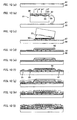
- the main process for creating a transistor is performed by forming a gate electrode 83, an impurity doped portion 84, and a gate insulating film 82 on a singlecrystalline Si substrate 81 through micro-fabrication.
- hydrogen ion of a predetermined concentration is implanted into the substrate with a predetermined depth so as to form an ion implantation section 85.
- An oxide film 86 is formed on the surface and is then flattened by CMP (Chemical Mechanical Polishing).
- the singlecrystalline Si substrate 81 is cut into a predetermined-shape, and is brought into contact with a glass substrate 88, which is thereon provided with a SiO 2 film 87 by a plasma CVD using TEOS (Si (OC 2 H 5 ) 4 : Tetra Ethyl Ortho Silicate) and having been activated by an SC1 cleaning solution or the like, so that the singlecrystalline Si substrate 81 and the glass substrate 88 are bonded.
- TEOS Si (OC 2 H 5 ) 4 : Tetra Ethyl Ortho Silicate
- the two mated substrates are heated to grow a Platelet, which contains hydrogen gas, in the hydrogen ion implantation section 85, the Platelet is then separated as a thin film of a singlecrystalline Si device 90.
- the singlecrystalline Si device 90 and a non-singlecrystalline Si TFT 91 coexist.
- this invention provides means to solve the conventional size restriction depending on the size of Si wafer.
- this method also allows omission of the step of forming a solid phase epitaxial film on the silicon dioxide (SiO 2 ), it is also possible to solve the defects of increase in time of fabrication, complication of fabrication and a decrease in yield (transfer process, division/retention of thin film, epitaxial growth) arisen in the conventional method, which first forms an operation region on a solid phase epitaxial film, which is a singlecrystalline layer of a thin film grown on a silicon dioxide (SiO 2 ) to become a singlecrystalline Si device, and then divides the silicon dioxide (SiO 2 ) by etching.
- the singlecrystalline Si when the singlecrystalline Si is eventually transferred onto an insulating substrate such as a glass substrate so as to form a device, the singlecrystalline Si becomes a thin film. Therefore, it is not necessary to create a complex well structure or to perform doping process for making, channel stop etc., which are required for a general bulk singlecrystalline Si LSI; however, there still are problems regarding device isolation, recovery of surface damage after creating a thin film, solution for realizing the short channel. Thus, it is necessary to create a new fabrication method or a new device structure to solve those problems.
- this method further has inadequacies in device isolation (defective Si island's end in island etching) and reduction in stress leakage current.
- the semiconductor substrate and the semiconductor device according to the present embodiment provide improved performance and improved functionality on account of a structure in which a MOS non-singlecrystalline Si thin film transistor and a MOS singlecrystalline Si thin film transistor are formed in different regions of an insulating substrate, such as a glass substrate.
- This semiconductor device is to be mounted to an active matrix substrate using TFTs (Thin Film Transistor).
- the MOS thin film transistor is a general transistor comprising an active layer, a gate electrode, a gate insulating film, and a high concentration impurity doped portion (source/drain electrodes) formed on each side of the gate, wherein the gate electrode controls the carrier density of the semiconductor layer under the gate, so as to control a flow of source-drain current.
- the MOS transistor when arranged as a CMOS (Complementary MOS) structure, consumes less power, and produces full output according to the power voltage. With this advantage, the MOS transistor is suitable for a low power consumption logic device.
- the present embodiment assumes a CMOS (Complementary MOS), but only one MOS (Metal Oxide Semiconductor) is illustrated in the accompanied figures.
- the semiconductor substrate 10 includes a singlecrystalline silicon (Si) wafer (Singlecrystalline Si wafer, hereinafter) 8 which is provided as a singlecrystalline Si substrate including neither well-structure nor channel stop structure; a gate insulating film 3 formed on the singlecrystalline Si wafer 8; a gate electrode 2 formed on the gate insulating film 3; and a LOCOS (Local Oxidation of Silicon: Selective Oxidation) oxide film 7; and a planarization insulating film 1 formed as an insulating film over the LOCOS oxide film 7 and the gate electrode 2.
- the singlecrystalline silicon wafer 8 includes an active layer 6 which has a channel region 17, and source/drain regions 4 and 5.
- the LOCOS oxide film 7 is formed on the singlecrystalline Si wafer 8 around the active layer 6, and has a thickness greater than the gate insulating film 3.
- the active layer 6 has N+ or P+ impurity implantation portion, where the source region 4 and the drain region 5 are formed. These impurity portions are formed in a device area in which a shallow reverse-conductive impurity is doped.
- the singlecrystalline Si wafer 8 is provided with a LDD (Lightly Doped Drain) structure (4a/5a), or implantation (doping) of either Pocket or Halo as a solution for realizing the short channel.
- LDD Lightly Doped Drain
- implantation doping
- the oxide film 1 is formed of a silicon dioxide (SiO 2 ) film, a phosphorous silicate glass (PSG) film or a borophospho-silicate glass (BPSG) film, for example.
- the LOCOS film is provided as one of the means for device isolation.
- the LOCOS film is usually formed as a thick thermal oxide film (field oxide film) around the active layer 6 so as to function as a thick insulating film for the gate electrode running across the field section, thereby increasing the threshold voltage of a parasitic transistor generated in the portion. In this way, the LOCOS film serves to isolate elements into separate areas, thus ensuring device isolation.
- the thickness of the LOCOS oxide film 7 ranges approximately from 30nm to 200nm. More specifically, compared with a conventional MOSLSI (Large Scale Integrated Circuit) using an oxide film whose thickness is approximately 500nm (at least 300nm) or greater, the LOCOS film of the present embodiment, to be grown to a field region 16, has a 1/2 or 1/10 thickness, i.e., approximately 30nm to 200nm. This thickness in the present embodiment relies on the fact that the portion of the parasitic transistor is removed from the Si film, that is, there will be no parasitic transistor generated in this structure.
- MOSLSI Large Scale Integrated Circuit
- This structure allows creation of a thin film device, which can coexist with a non-singlecrystalline Si on the insulating substrate such as a large glass substrate.
- This structure also achieves great reduction in time for oxidization, besides the oxidization can be carried out not in a wet method but in a dry method at a practically satisfactory level.
- the stress due to oxidization in the edge of the oxide film is greatly reduced, the characteristics of the transistor become stable.
- the thin oxide film helps reduction of Bird's Beak, thus providing a minute device area in the transistor with high accuracy.
- an ion implantation layer 9 is formed on the singlecrystalline Si wafer 8 with a predetermined depth, inside the active layer 6.
- This ion implantation layer 9 is formed by implanting either or both of hydrogen ion and inactive element ion such as helium (He) ion, having a predetermined concentration.
- He helium
- the semiconductor substrate 10 may include at least one metal wiring layer, as shown in Figure 2.
- this semiconductor substrate 10 includes a gate electrode 2 formed on the planarization insulating film 1; a gate insulating film 3 formed on the gate electrode 2, an active layer 6 not containing a well-structure, formed on the gate insulating film 3; a LOCOS oxide film 7; a protective-insulating-interlayer film 21 formed over the active layer 6 and the LOCOS oxide film 7; and metal wiring layers 23 formed on the surface of the protective-insulating-interlayer film 21.
- the active layer 6 is made of a singlecrystalline Si having impurity implantation portions of N+ or P+, which are to be the source/drain regions 4/5. These impurity portions are formed in the element-forming-region in which a shallow reverse-conductive impurity is doped.
- the LOCOS oxide film 7 is formed around the active layer 6.
- the metal wiring layers 23 are connected to the source and drain regions 4 and 5, respectively, through contact holes 22 which are formed on the protective-insulating-interlayer film 21 to establish conduction.
- the semiconductor device 30 of the present embodiment is formed by bonding the semiconductor substrate 10 onto an insulating substrate 25. More specifically, as shown in the figure, in the semiconductor device 30, a semiconductor device 10 is formed on the insulating substrate 25 through a silicon dioxide film (SiO 2 ) 26 which is formed by plasma CVD using TEOS (Si (OC 2 H 5 ) 4 :Tetra Ethyl Ortho Silicate).
- SiO 2 silicon dioxide film
- TEOS Si (OC 2 H 5 ) 4 :Tetra Ethyl Ortho Silicate
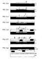
- a singlecrystalline Si wafer 8 made of a singlecrystalline silicon (Si) is prepared, and its surface is subjected to oxidization so as to form a thin silicon dioxide (SiO 2 ) film 11 with a thickness of about 30nm.
- a silicon nitride (SiN) film 12 is deposited over the silicon dioxide (SiO 2 ) 11 by plasma CVD (Chemical Vapor deposition), and then, the silicon nitride (SiN) film 12 is removed by etching except for the device area.
- a LOCOS oxide film 7 is grown by dry oxidization.
- the silicon nitride (SiN) film 12 is removed by etching, and boron (B) and phosphorous (P) are implanted in the device area 13 surrounded by the LOCOS oxide film 7, which is a field oxide film, for adjustment of the threshold voltage in the N/P channel regions; and then, the silicon dioxide (SiO 2 ) film 11 is removed. More specifically, in the device area 13, implantation of boron (B) ion creates a P-region, where, as described later, arsenic (As) ion is further implanted to form the source and drain regions 4 and 5 to form a N-type MOS transistor.
- boron (B) ion creates a P-region, where, as described later, arsenic (As) ion is further implanted to form the source and drain regions 4 and 5 to form a N-type MOS transistor.
- a P-type MOS transistor is formed.
- the N-type MOS transistor and the P-type MOS transistor are formed at the same time, to be a CMOS transistor.
- the region having the channel region (the region beneath the gate electrode 2), the source region 4, and the drain region 5 becomes the active layer 6. Further, an impurity ion is implanted in the channel region beneath the gate electrode 2, so as to adjust the threshold voltage.
- a 15nm thick silicon dioxide (SiO 2 ) is deposited by dry oxidization to form the gate insulating film 3.
- a polycrystalline silicon (Si) (Poly-Si, hereinafter) or the like is formed on the gate insulating film 3, with a thickness of about 300nm, then, phosphorous oxychloride (POCl 3 : not shown) is deposited thereon, and heated at 850 °C for diffusion.
- the product is patterned to form the gate electrode 2, and boron (B) or phosphorous (P) is implanted to form the LDD structures 4a and 5a.
- a silicon dioxide (SiO 2 ) of about 300nm is deposited thereon, which is then etched back by reaction ion etching (RIE) to form the side walls 15.
- RIE reaction ion etching
- arsenic (As) ion or boron fluorine (BF 2 ) ion is implanted to form the source and drain regions, followed by activation annealing at about 900°C, thereby forming the source region 4 and the drain region 5.
- a silicon dioxide (SiO 2 ) with a thickness of about 100nm is deposited by APCVD (Atmospheric Pressure CVD), and a silicon dioxide (SiO 2 ) with a thickness of about 400nm is further deposited by PECVD (Plasma Enhanced CVD) using TEOS, which is then polished by CMP (Chemical Mechanical Polishing) for about 100nm to flatten the surface, thereby forming a planarization insulating film 1.
- hydrogen (H) ion or the like is implanted into the singlecrystalline Si wafer 8 through the planarization insulating film 1.
- hydrogen (H) ion with a dose of 5.5 ⁇ 10 16 cm -2 is implanted in the ion implantation layer 9 at 100keV.
- the hydrogen (H) ion is not limited to this, but may be helium (He) ion or the like.
- the power for implantation is adjusted so that the resulting ion implantation layer 9 formed in the active layer 6 of singlecrystalline Si extends into the Si crystal beneath the LOCOS oxide film 7.
- the substrate turned upside down, and is subjected to washing and surface activation together with another insulating substrate 25 on which a silicon dioxide (SiO 2 ) with a thickness of about 100nm is formed by a plasma CVD using TEOS and oxygen gas.
- the washing and surface activation is performed by megasonic shower of a mixture liquid (SCI liquid) of ammonia water, hydrogen peroxide solution and pure water.
- the substrate 10 is bonded to the insulating substrate 25 in accordance with the marker (not shown) on the planarization insulating film 1, as shown in Figure 4(a).
- the insulating substrate 25 is bonded because of the planarization insulating film 1, Van der Waals force and hydrogen bond.
- the surface may be activated by being exposed in oxygen plasma atmosphere.
- the insulating substrate 25 has the same size as the semiconductor substrate 10, but it may be a larger glass substrate whose area corresponds to a large number of semiconductor substrates 10.
- the insulating substrate 25 is made of a glass, for example, "code 1737", a product of Corning (alkali-earth alumino-boro-sillicated glass).
- the combined body is subjected to annealing at about 250°C for two hours to ensure the bonding. Thereafter, through heat treatment at about 600°C for three minutes, the body is cleaved at the ion implantation layer (projection range of ion implantation) 9 so as to separate the singlecrystallinc Si wafer 8, as shown in Figure 4(b).
- a silicon dioxide (SiO 2 ) with a thickness of about 100nm is deposited on the divided surface by plasma CVD, and is etched back by reaction ion etching (RIE).
- RIE reaction ion etching
- mixture gas of carbonfluoride (CF 4 ) and hydrogen is used.
- the mixture gas is replaced with another mixture gas of carbon-fluorine (CF 4 ) and oxygen, and the reaction ion etching is continued.
- the etching is stopped when the singlecrystalline Si film is all removed from the LOCOS oxide film 7 as the filed oxide film.
- the etching is stopped after a certain time elapsed, which time was decided in advance based on the etching rate.
- the surface is lightly etched with buffered hydrogen fluoride (HF), and the substrate is heated to 380°C. Then a silicon dioxide (SiO2) of about 400nm is deposited by PECVD using TEOS to form a protective-insulating-interlayer film 21.
- HF buffered hydrogen fluoride
- the contact holes 22 are created on the protective-insulating-interlayer film 21, and a material for metal wiring is deposited therein to form the metal wiring layers 23.
- This embodiment uses Ti/TiN/Al-Si/TiN/Ti, whose total thickness is about 400nm. Then, the material is patterned into a predetermined shape. Consequently, as shown in Figure 2, a semiconductor device 30 including many singlecrystalline Si TFTs is formed on the insulating substrate 25.
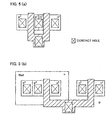
- CMOS inverter as the basic circuit element of the semiconductor device thus fabricated is shown in Figure 5(a). As can be seen in the figure, this CMOS inverter has a lot smaller area than the conventional CMOS inverter shown in Figure 5(b).
- the semiconductor substrate 10 of the present embodiment is a singlecrystalline Si MOS transistor formed on a device area surrounded by a thin field oxide film. Because of the omission of well structure, the configuration becomes simple, thereby achieving an increase in yield and a decrease in cost. Though this semiconductor substrate does not operate alone, it ensures high performance when transferred onto the insulating substrate 25, which is made of a different glass substrate or the like. Further, the semiconductor device 30 includes a SiO 2 film, a MOS non-singlecrystalline Si thin film transistor including a non-singlecrystalline Si thin film made of a polycrystalline Si, a MOS singlecrystalline Si thin film transistor including a singlecrystalline Si thin film, and metal wiring.
- a thin film device which can coexist with a non-singlecrystalline Si, is transferred onto, for example, a large glass substrate in the following manner.
- boron ion or phosphorous ion with a predetermined concentration is implanted in an area, which is surrounded by the field oxide film and becomes either a n-channel area or a p-channel area, so as to adjust the threshold voltage.
- the gate insulating film 3, and the gate electrode 2 are formed, and if necessary, LDD, HALO or Pocket implantation is carried out. Further, N+ or P+ is implanted to form the source/drain regions 4/5, and a planarization film is formed.
- Hydrogen ion or He ion with a predetermined concentration is implanted alone or together with He, Ne or the like to a predetermined depth.
- the substrate is then cut into a predetermined shape, and the surface is activated by oxygen plasma, hydrogen peroxide solution, or RCA1 cleaning solution (SC1).
- SC1 cleaning solution SC1
- the substrate is then closely brought into contact with an insulating substrate 25 on which a part or the whole non-singlecrystalline Si TFT is formed, followed by bonding and heat treatment.
- the bulk singlecrystalline Si portion is cleaved at the ion implantation layer 9 to become a thin film.
- the surface of the singlecrystalline Si is etched back by RIE (reactive ion etching) to shape the substrate into a thin film, and the etching is continued until the Si film is all removed from the LOCOS oxide film 7. In this manner, it is possible to create the minute transistor region without accurate positioning, thereby ensuring device isolation.
- RIE reactive ion etching
- a silicon dioxide (SiO 2 ) film on the thin film of the singlecrystalline Si, thus created through the cleavage, through PECVD using TEOS or the like, and etching back the film by etchant gas, which has a composition (e.g., CF 4 and hydrogen) allowing to the whole film, including the deposited oxide film and the singlecrystalline Si film, to have a predetermined thickness, the surface of the film is flattened and the leak current is reduced in the resulting device.
- etchant gas which has a composition (e.g., CF 4 and hydrogen)
- This process allows omission of well-structure, ion implantation for channel stop or the like, well contact region etc., which are required in a common MOSLSI, thus allowing great simplification in space and process.
- the thickness of the singlecrystalline Si thin film becomes substantially 1/2 of the whole thickness of the Si oxide film (LOLOS oxide film 7) formed around the active layer 6, so that the pattern edge of the singlecrystalline Si thin film almost matches with the inclination of the pattern edge of the Si oxide film around the active layer 6.
- the protective-insulating-interlayer film 21 is deposited thereon, the contact holes 22 are further formed therein, and the metal wiring layer 23 is formed. The device is here completed.
- the protective-insulating-interlayer film 21 is made of a protection insulating film and an interlayer insulating film, which may be formed of the same material as long as their function and characteristics are ensured.
- metal wiring which is formed of a metal with a high melting point, and is not easily oxidized; then, a planarization film is deposited thereon, whose surface is flattened by CMP or the like to make an appropriate condition for combining with the insulating substrate 25, before bonded to the insulating substrate 25, and the bulk Si is cleaved through heat treatment. In this manner, it is possible to realize both miniaturization and higher integration density.
- an active layer 6 having a channel region 17, a source region 4, and a drain region 5; and a singlecrystalline Si wafer 8 including at least a part of a device structure not containing a well-structure or a channel stop region is used.
- the resulting semiconductor device is superior in performance and less varied in characteristic.
- the area of the device area 13 is reduced, allowing more dense integration, thereby realizing a highly-dense semiconductor substrate 10.
- the transistor since the conventional well is omitted, the transistor may be made thinner than the conventional structure using a well.
- the semiconductor element can be made as a thin film which can coexist with the TFTs formed from other polycrystalline Si upon formation of the semiconductor device 30, allowing conduction between the semiconductor element and TFTs through common thin film wiring. Further, since the element is made as a thin film, it is possible to ensure the device isolation of the minute singlecrystalline Si device even on the insulating substrate 25, such as a large glass substrate, without highly-accurate photolithography. Further, since the well is omitted, the fabrication process is simplified.
- the LOCOS oxide film 7, thicker than the gate insulating film 3, is formed by surrounding the active layer 6. This LOCOS oxide film 7 securely ensures the device isolation.
- the process for making the singlecrystalline Si is simplified. Further, the foregoing arrangement provides a semiconductor substrate and a fabrication method thereof, which ensures device isolation of the minute singlecrystalline Si semiconductor element without highly-accurate photolithography, when the singlecrystalline Si semiconductor element is transferred onto the large insulating substrate 25. Note that, though the present embodiment uses a large insulating substrate 25, the present invention may use a smaller insulating substrate.
- the source region and the drain region of the active layer at least have a LDD structure. Therefore, the change in density distribution of impurities in the vicinity of the drain becomes less rapid, and the electric field strength in the vicinity of the drain region 5 is reduced, thereby improving reliability.
- the planarization insulating film 1 has a flat upper surface.
- the insulating substrate 25, which is realized by a flat glass substrate or the like, may be bonded to the planarization insulating film 1.
- the LOCOS film which is to be grown to a field region 16 has a 1/2 or 1/10 thickness, i.e., approximately 30nm to 200nm.
- This structure achieves great reduction in time for oxidization, besides the oxidization can be carried out not in a wet method but in a dry method at a practically satisfactory level. Particularly, since the stress due to oxidization in the edge of the oxide film is greatly reduced, the characteristics of the transistor become stable. Further, the thin oxide film helps reduction of Bird's Beak, thus providing a minute device area in the transistor with high accuracy.
- an ion implantation layer is formed in the singlecrystalline Si substrate with a predetermined depth through implantation of one or plural kinds of ion selected from a hydrogen ion group or an inactive element ion group.
- the wafer is cleaved at the ion implantation layer 9 by heat treatment.
- the ion implantation layer 9 formed in the singlecrystalline Si wafer 8 with a predetermined depth is formed in a portion lower than the LOCOS oxide film 7.
- the surface is flattened. With this arrangement, the leak current is reduced in the resulting device.
- the LOCOS oxide film 7 is a thin film, which can be formed by dry oxidation. Therefore, it is possible to greatly reduce the stress upon oxidization of ends of the oxide film, thereby obtaining a transistor with stable characteristics.
- semiconductor device 30 of the present embodiment includes the insulating substrate 25, and a singlecrystalline Si semiconductor element formed on the insulating substrate 25.
- the semiconductor device 30 is realized by, for example, a glass insulating substrate 25 and a singlecrystalline Si semiconductor element combined together.
- the singlecrystalline Si semiconductor element comprising a gate electrode 2 formed above the insulating substrate 25; a gate insulating film 3 formed on the gate electrode 2; an active layer 6, which is formed on the gate insulating film 3 and is made of a singlecrystalline Si layer having a channel region 17, a source region 4, and a drain region 5; a LOCOS oxide film 7 formed around the active layer 16; and an interlayer insulating film 21 formed over the active layer 6 and the LOCOS oxide film 7.
- the semiconductor device 30 having a high-performance integration system by forming the non-singlecrystalline Si semiconductor element and the singlecrystalline Si semiconductor element on the large insulating substrate 25, the process for making the singlecrystalline Si is simplified. Further, the foregoing arrangement provides a semiconductor substrate and a fabrication method thereof, which ensures device isolation of the minute singlecrystalline Si semiconductor element without highly-accurate photolithography, when the singlecrystalline Si semiconductor element is transferred onto the large insulating substrate 25.
- the semiconductor device 30 includes a metal wiring layer 23, which is formed on the protective-insulating-interlaycr film 21 and is connected to the source and drain regions 4 and 5 via contact holes 22 formed in the protective-insulating-interlayer film 21.
- a fabrication method of a semiconductor device 30 comprises the steps of: (a) bonding the semiconductor substrate 10, formed by the foregoing fabrication method of the semiconductor substrate 10, onto the insulating substrate 25, (b) dividing the singlecrystalline Si substrate at the ion implantation layer 9 by heat treatment so as to detach a part of the singlecrystalline Si wafer 8; (c) etching a part of the singlecrystalline Si on the insulating substrate 25 so as to expose a surface of the LOCOS oxide film 7; (d) forming an the protective-insulating-interlayer film 21 over the active layer 6 and the LOCOS oxide film 7; and (e) forming a metal wiring layer 23 on the protective-insulating-interlayer film 21, and connecting the metal wiring layer 23 to the source and drain regions 4 and 5 via contact holes 22, which is formed in the protective-insulating-interlayer film 21.
- the foregoing arrangement includes a metal wiring layer 23, which is formed on the protective-insulating-interlayer film 21 and is connected to the source and drain regions 4 and 5 via contact holes 22 formed in the protective-insulating-interlayer film 21.
- the semiconductor device 30 is conducted to other circuits, power supply etc. through this metal wiring layer 23.
- the metal wiring layer 23 can be formed after the semiconductor substrate 10 having the singlecrystalline Si semiconductor element is bonded to the insulating substrate 25.
- the semiconductor device 30 having a high-performance integration system by forming the non-singlecrystalline Si semiconductor element and the singlecrystalline Si semiconductor element on the large insulating substrate 25, the process for making the singlecrystalline Si is simplified. Further, the foregoing arrangement provides a semiconductor substrate and a fabrication method thereof, which ensures device isolation of the minute singlecrystalline Si semiconductor element without highly-accurate photolithography, when the singlecrystalline Si semiconductor element is transferred onto the large insulating substrate 25.
- the upper surface of the active layer 6 exists lower than the upper surface of the LOCOS oxide film 7, because the surface of the singlecrystalline Si thin film, which became a thin film by cleavage, is etched back to be lower than the surface of the LOCOS oxide film 7 to be a flat plane. With this arrangement, the leak current is reduced in the resulting device.
- both edges of the active layer lie along inclinations of edges of the LOCOS oxide film.
- the singlecrystalline Si semiconductor element is formed in one portion of the insulating substrate, and a non-singlecrystalline Si semiconductor element is formed on another portion of the insulating substrate.
- This arrangement allows coexistence of a singlecrystalline Si semiconductor element and a non-singlecrystalline Si semiconductor element on the insulating substrate 25.
- switching transistors for the pixels arc formed of non-singlecrystalline Si semiconductor elements on the insulating substrate 25 of glass or the like. Then, after the wiring pattern for the transistors are formed, the display drive circuit for driving the display section and/or the processing circuit for outputting predetermined signals to the display drive circuit is provided in the from of COG or COF realized by the singlecrystalline Si semiconductor element, and the circuit is then connected to the wiring pattern.
- the singlecrystalline Si semiconductor element constitutes the switching transistor which controls display of each pixel constituting a display section 71
- the transistor constituted of the singlecrystalline Si semiconductor element constitutes either a display drive circuit 72/73 for driving the display section, or a processing circuit 74/75 for outputting a predetermined signal to the display drive circuit 72/73; further, the transistor is also used as a substrate for constituting the display device 70.
- surfaces of the semiconductor substrate 10 and the insulating substrate 25 are activated through either washing by cleaning water containing a hydrogen peroxide solution, or by exposure under oxygen-plasma atmosphere.
- the semiconductor substrate 10 and the insulating substrate 25 are bonded by Van der Waals or hydrogen bond, without an adhesive. Note that, this bonding becomes a firm Si-O coupling through the heat treatment performed thereafter.
- the heat treatment in the singlecrystalline Si substrate removal process is carried out at a temperature ranging approximately from 250°C to 600°C.
- the singlecrystalline Si semiconductor element is heated to, for example, a temperature at which the hydrogen ion is separated from the Si, thus securing the bonding strength between the semiconductor substrate and the insulating substrate 25; further, the heat causes the wafer body to be cleaved at the ion implantation layer 9, detaching a part of the singlecrystalline Si wafer 8.
- the metal wiring layers 23 as external electrodes are connected directly to the source and drain regions 4 and 5 through contact holes 22 of the protective-insulating-interlayer film 21.
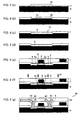
- the first metal wiring 42 which is the first wiring layer for making conduction with the source/drain region 4/5, is first lead to the rear surface of the semiconductor substrate 40 and the semiconductor device 50 (both described later), and then is drawn back onto the surface of the semiconductor substrate 40 and the semiconductor device 50 in the field region 16 formed around the device area 13, as second metal wiring 45, which is a second wiring layer.
- the semiconductor substrate 40 includes an insulating substrate 25 and a singlecrystalline Si semiconductor element formed on the insulating substrate 25.
- the singlecrystalline Si semiconductor element includes; a gate electrode 2 formed above the insulating substrate 25; a gate insulating film 3 formed on the gate electrode 2; an active layer 6 formed of a singlecrystalline Si layer, having a channel region 17 and source / drain regions 4 and 5, formed on the gate insulating film 3; and a LOCOS oxide film 7 formed around the active layer 6; and a protective-insulating-interlayer film 21 formed over the active layer 6 and the LOCOS oxide film 7.
- the singlecrystalline Si semiconductor element further includes; an interlayer insulating film 43; at least one first metal wiring 42 formed on the upper surface of the interlayer insulating film 43; and a second metal witing 45, formed on the protective-insulating-interlayer film 21, being connected to the first metal wiring 42.
- the active layer 6 is made of a singlecrystalline Si.
- the active layer 6 does not include a well structure, and is provided with N+ or P+ impurity implantation portion, where the source region 4 and the drain region 5 are formed. These impurity portions are formed in a device area in which a shallow reverse-conductive impurity is doped.
- the first metal wirings 42 are connected to the source and drain regions 4 and 5, respectively, through contact holes 41 which are formed on the insulating film 1 and the gate insulating film 3 to establish conduction.
- the other end of each first metal wiring 42 is exposed to the rear surface of the insulating film 1.
- the second metal wiring 45 being formed on the surface of the protective-insulating-interlayer film 21 through contact holes 44 which is formed on the insulating film 1, the gate insulating film 3, and the protective-insulating-interlayer film 21 to establish conduction, is connected to the first metal wiring 42.
- the semiconductor device 50 is formed by mounting the foregoing semiconductor substrate 40 onto the insulating substrate 25, such as a glass substrate. More specifically, the semiconductor device 50 is mounted on the insulating substrate 25 through a silicon dioxide film (SiO 2 ) 26 which is formed by plasma CVD using TEOS.
- SiO 2 silicon dioxide film
- a singlecrystalline Si wafer 8 made of a singlecrystalline silicon (Si) is prepared, and its surface is subjected to oxidization so as to form a thin silicon dioxide (SiO 2 ) film 11 with a thickness of about 30nm.
- a silicon nitride (SiN) film 12 is deposited over the silicon dioxide (SiO 2 ) 11 by plasma CVD (Chemical Vapor deposition), and then, the silicon nitride (SiN) film 12 is removed by etching except for the device area.
- a LOCOS oxide film 7 is grown by dry oxidization.
- the silicon nitride (SiN) film 12 is removed by etching, and boron (B) and phosphorous (P) are implanted in the device area 13 surrounded by the LOCOS oxide film 7, which is a field oxide film, for adjustment of the threshold voltage in the N/P channel regions; and then, the silicon dioxide (SiO 2 ) film 11 is removed.
- the region having the channel region (the region beneath the gate electrode 2), the source region 4, and the drain region 5 becomes the active layer 6. Further, an impurity ion is implanted in the channel region beneath the gate electrode 2, so as to adjust the threshold voltage.
- a 15nm thick silicon dioxide (SiO 2 ) is deposited by dry oxidization to form the gate insulating film 3.
- a polycrystalline silicon (Si) (Poly-Si, hereinafter) or the like is formed on the gate insulating film 3, with a thickness of about 300nm, then, phosphorous oxychloride (POCl 3 : not shown) is deposited thereon, and heated at 800 °C for diffusion.
- the product is patterned to form the gate electrode 2, and boron (B) or phosphorous (P) is implanted to form the LDD structures 4a and 5a.
- a silicon dioxide (SiO 2 ) of about 300nm is deposited thereon, which is then etched back by reaction ion etching (RIE) to form the side walls 15.
- RIE reaction ion etching
- arsenic (As) ion or boron fluorine (BF 2 ) ion is implanted to form the source and drain regions, followed by activation annealing at about 900°C, thereby forming the source region 4 and the drain region 5.
- a silicon dioxide (SiO 2 ) with a thickness of about 100nm is deposited by APCVD (Atmospheric Pressure CVD), and a silicon dioxide (SiO 2 ) with a thickness of about 400nm is further deposited by PECVD (Plasma Enhanced CVD) using TEOS, which is then polished by CMP (Chemical Mechanical Polishing) for about 100nm to flatten the surface, thereby forming a planarization insulating film 1.
- hydrogen (H) ion is implanted into the singlecrystalline Si wafer 8 through the insulating film 1.
- hydrogen (H) ion with a dose of 5.5 ⁇ 10 16 cm -2 is implanted in the ion implantation layer 9 at 100keV.
- the hydrogen (H) ion is not limited to this, but may be helium (He) ion or the like.
- the power for implantation is adjusted so that the resulting ion implantation layer 9 formed in the active layer 6 of singlecrystalline Si extends into the Si crystal beneath the LOCOS oxide film 7.
- a 200nm thick silicon dioxide (SiO 2 ) is further formed thereon, the contact holes 41 are made, and a material for metal wiring is deposited therein to form the first metal wirings 42.
- the first metal wirings 42 is made as a layer of Ti/TiN/Ti, with s total thickness of about 400nm. Then, the material is patterned into a predetermined shape.
- a silicon dioxide (SiO 2 ) with a thickness of about 400nm is deposited thereon by PECVD using TEOS, and then the layer is etched back by reaction ion etching (RIE), except for the first metal wirings 42. Further, 500nm thick silicon oxide (SiO 2 ) is deposited thereon, which is then flattened by CMP to become the interlayer insulating film 43.
- SiO 2 silicon dioxide
- RIE reaction ion etching
- the wafer is cut into a predetermined shape, and is subjected to washing and surface activation together with another insulating substrate 25 on which a silicon dioxide (SiO 2 ) with a thickness of about 100nm is formed by a plasma CVD using TEOS and oxygen gas.
- the washing and surface activation is performed by megasonic shower of a mixture liquid (SCI liquid).
- the wafer is closely brought into contact with the insulating substrate 25 to be bonded thereto in accordance with the marker (not shown) on the interlayer insulating film 43, as shown in Figure 10(b).
- the insulating substrate 25 is bonded because of the insulating film 1, Van der Waals force or hydrogen bond.
- the insulating substrate 25 has the same size as the semiconductor substrate 40, but it is actually a large glass substrate whose area is larger than the total area of the large number of semiconductor substrates 10.
- the insulating substrate 25 is made of a glass, for example, "code 1737", a product of Corning (alkali-earth alumino-boro-sillicated glass).
- the combined body is subjected to annealing at about 250°C for two hours to ensure the bonding. Thereafter, through heat treatment at about 600°C for three minutes, the body is cleaved at the ion implantation layer (peak position of ion implantation) 9 so as to separate the singlecrystalline Si wafer 8, as shown in Figure 10(c).
- a silicon dioxide (SiO 2 ) with a thickness of about 100nm is deposited on the divided surface by plasma CVD, and is etched back by reaction ion etching (RIE).
- RIE reaction ion etching
- mixture gas of carbon-fluorine (CF 4 ) and hydrogen is used.
- the mixture gas is replaced with another mixture gas of carbon-fluorine (CF 4 ) and oxygen, and the reaction ion etching is continued.
- the etching is stopped when the singlecrystalline Si wafer 8 is all removed from the LOCOS oxide film 7 as the filed oxide film.
- the etching is stopped after a certain time elapsed, which time was decided in advance based on the etching rate.
- the surface is lightly etched with buffer hydrogen fluoride (HF), and the substrate is heated to 380°C. Then a silicon dioxide (Si02) of about 400nm is deposited by PECVD using TEOS to form a protective-insulating-interlayer film 21.
- HF buffer hydrogen fluoride
- the contact holes 41 are created on the protective-insulating-interlayer film 21, and a material for metal wiring is deposited therein to form the second metal wiring 45.
- This embodiment uses Ti/TiN/Al-Si/TiN/Ti, whose total thickness is about 400nm. Then, the material is patterned into a predetermined shape. Consequently, as shown in Figure 8, a semiconductor device 50 including a singlecrystalline Si semiconductor device is formed on the insulating substrate 25.
- the first metal wiring 42 is directly connected to the second metal wiring 45; however, the metal wiring 45 may be arranged differently, for example, it may be connected to the metal wiring layer 42 via a relay electrode made of a gate layer 2a. In this case, the contact hole for connecting the second metal wiring 45 to the relay electrode of gate 2a can be made shallow, and the yield is increased. More specifically, the first metal wiring 42 is connected to the relay electrode made of a gate 2a, while its rear surface is connected to the second wiring 45.
- the semiconductor substrate 40 includes an insulating substrate 25 and a singlecrystalline Si semiconductor element formed on the insulating substrate 25.
- the singlecrystalline Si semiconductor element includes a gate electrode 2 formed above the insulating substrate 25; a gate insulating film 3 formed on the gate electrode 2; an active layer 6; and a LOCOS oxide film 7 formed around the active layer 6; and a protective-insulating-interlayer film 21 over the active layer 6 and the LOCOS oxide film 7.
- the active layer 6 includes a channel region 17, and source/drain regions 4 and 5.
- the singlecrystalline Si semiconductor element further includes; an interlayer insulating film 43, which is an insulating film formed between the insulating substrate 25 and the gate electrode 2; at least one first metal wiring 42 formed on the upper surface of the interlayer insulating film 43; and a second metal witing 45, formed on the protective-insulating-interlayer film 21, being connected to the first metal wiring 42.
- an interlayer insulating film 43 which is an insulating film formed between the insulating substrate 25 and the gate electrode 2
- a second metal witing 45 formed on the protective-insulating-interlayer film 21, being connected to the first metal wiring 42.
- This method allows creation of the semiconductor device 50 including the second metal wiring 45. Further, by combining the semiconductor substrate 40 with the insulating substrate 25, the semiconductor device 50 is created.
- the first metal wiring 42 On forming the first metal wiring 42, it is generally required to form a plurality of wiring layers for efficient use of space, in order to increase the integration density of the IC. However, this results from difficulty in providing wiring pattern due to the small element region.
- the semiconductor substrate 40/semiconductor device 50 includes at least one first metal wiring 42 formed beneath the planarization insulating film 1; and a second metal witing 45, formed on the protective-insulating-interlayer film 21, being connected to the first metal wiring 42.
- At least one first metal wiring 42 is formed on the planarization insulating film 1, and this metal wiring can be used as an external leading electrode of the source/drain regions 4/5.
- the first metal wiring 42 is a single layer, however, it may be provided as a plurality of layers.
- the first metal wiring 42 is made of a material whose heat-resistant temperature (the lower one of (i) the melting point and (ii) the reaction temperature with Si) is about 500°C or greater. On this account, the first metal wiring 42 is not fused during the fabrication.
- an active layer having a channel region, a source region, and a drain region; and the singlecrystalline Si substrate includes at least a part of a device structure not containing a well-structure or a channel stop region.
- the area of the device area is reduced, allowing more dense integration, thereby realizing a highly-dense semiconductor substrate.
- the resistor may be made thinner than the conventional structure using a well.
- the semiconductor element can be made as a thin film which can coexist with the TFTs formed from other polycrystalline Si upon formation of the semiconductor device, allowing conduction between the semiconductor element and TFTs through common thin film wiring Further, since the element can be isolated by etching back the Si thin film, which is created as a result of the cleavage, it is possible to ensure the device isolation of the minute singlecrystalline Si device even on the insulating substrate 25, such as a large glass substrate, without highly-accurate photolithography. Further, since the well is omitted, the fabrication process is simplified.
- the LOCOS oxide film thicker than the gate insulating film, is formed by surrounding the active layer. This LOCOS oxide film securely ensures the device isolation.
- the process for making the singlecrystalline Si is simplified. Further, the foregoing arrangement provides a semiconductor substrate and a fabrication method thereof, which ensures device isolation of the minute singlecrystalline Si semiconductor element without highly-accurate photolithography, when the singlecrystalline Si semiconductor element is transferred onto the large insulating substrate.
- the source and drain regions of the active layer form a LDD structure.
- the change in density distribution of impurities in the vicinity of the drain becomes less rapid, and the electric field strength in the vicinity of the drain region is reduced, thereby improving reliability.
- the surface of the insulating film is highly flat by CMP.
- the insulating substrate 25 which is realized by a flat glass substrate or the like, may be bonded to the planarization insulating film 1.
- At least one wiring layer is formed on the insulating film:
- This wiring enables conduction with other circuits, power supply etc.
- the LOCOS oxide film has a thickness of not less than 30nm and not more than 200nm.
- the LOCOS film in contrast to a conventional MOSLSI (Large Scale Integrated Circuit) using an oxide film whose thickness is approximately 500nm (at least 300nm) or greater, the LOCOS film, which is to be grown to a field region, has a 1/2 or 1/10 thickness, i.e., approximately 30nm to 200nm.
- MOSLSI Large Scale Integrated Circuit
- This structure achieves great reduction in time for oxidization, besides the oxidization can be carried out not in a wet method but in a dry method at a practically satisfactory level. Particularly, since the stress due to oxidization in the edge of the oxide film is greatly reduced, the characteristics of the transistor become stable. Further, the thin oxide film helps reduction of Bird's Beak, thus providing a minute device area in the transistor with high accuracy.
- an ion implantation layer is formed in the singlecrystalline Si substrate with a predetermined depth through implantation of one or plural kinds of ion selected from a hydrogen ion group or an inactive element ion group.
- the predetermined depth is decided according to the desired thickness of the singlecrystalline Si substrate.
- the wafer is cleaved at the ion implantation layer 9 by heat treatment.
- This structure allows transfer of a thin film device, which can coexist with a non-singlecrystalline Si, onto a large insulating substrate or the like.
- the ion implantation layer formed in the singlecrystalline Si substrate with a predetermined depth is formed in a portion lower than the LOCOS oxide film.
- the LOCOS oxide film is formed by dry oxidization.
- an upper surface of the active layer is lower than an upper surface of the LOCOS oxide film.
- both edges of the active layer lie along inclinations of edges of the LOCOS oxide film.
- the first wiring layer is made of a material whose heat-resistant temperature is about 500°C or greater, the heat-resistant temperature being a lower one of (i) a melting point and (ii) a reaction temperature with Si.
- the first wiring layer is not fused in the fabrication.
- the singlecrystalline Si semiconductor element is formed in one portion of the insulating substrate, and a non-singlecrystalline Si semiconductor element is formed on another portion of the insulating substrate.
- This arrangement allows coexistence of a singlecrystalline Si semiconductor element and a non-singlecrystalline Si semiconductor element on the insulating substrate.
- a semiconductor device is arranged so that a part of the singlecrystalline Si semiconductor element constitutes a transistor which controls display of a pixel constituting a display section, and the transistor constituted of the singlecrystalline Si semiconductor element constitutes either a display drive circuit for driving the display section, and/or a processing circuit for outputting a predetermined signal to the display drive circuit, the transistor being monolithically formed on a substrate constituting the display section; further, the transistor is also used as a circuit for constituting the display device.
- switching transistors for the pixels are formed of non-singlecrystalline Si semiconductor elements on the insulating substrate of glass or the like. Then, after the wiring pattern for the transistors are formed, the display drive circuit for driving the display section and/or the processing circuit for outputting predetermined signals to the display drive circuit is provided in the from of COG or COF realized by the singlecrystalline Si semiconductor element, and the circuit is then connected to the wiring pattern, otherwise, the display drive circuit and/or the processing circuit is externally provided from a print board or the like.
- the singlecrystalline Si semiconductor element constitutes the switching transistor which controls display of each pixel constituting a display section
- the transistor constituted of the singlecrystalline Si semiconductor element constitutes either a display drive circuit for driving the display section, or a processing circuit for outputting a predetermined signal to the display drive circuit.
- surfaces of the semiconductor substrate and the insulating substrate are activated through either washing by cleaning water containing a hydrogen peroxide solution, or by exposure under oxygen-plasma atmosphere.
- the semiconductor substrate and the insulating substrate are bonded by Van der Waals, hydrogen bond or other kinds of coupling, without an adhesive.
- the heat treatment in the singlecrystalline Si substrate removal process is carried out at a temperature ranging approximately from 250°C to 600°C.
- the singlecrystalline Si semiconductor element is heated to, for example, a temperature at which the hydrogen ion is separated from the Si, thus securing the bonding strength between the semiconductor substrate and the insulating substrate; further, the heat causes the wafer body to be cleaved at the ion implantation layer, detaching a part of the singlecrystalline Si substrate.
Landscapes
- Thin Film Transistor (AREA)
- Liquid Crystal (AREA)
- Local Oxidation Of Silicon (AREA)
- Devices For Indicating Variable Information By Combining Individual Elements (AREA)
- Element Separation (AREA)
- Metal-Oxide And Bipolar Metal-Oxide Semiconductor Integrated Circuits (AREA)
Applications Claiming Priority (2)
| Application Number | Priority Date | Filing Date | Title |
|---|---|---|---|
| JP2004093694A JP4319078B2 (ja) | 2004-03-26 | 2004-03-26 | 半導体装置の製造方法 |
| JP2004093694 | 2004-03-26 |
Publications (2)
| Publication Number | Publication Date |
|---|---|
| EP1580813A2 true EP1580813A2 (de) | 2005-09-28 |
| EP1580813A3 EP1580813A3 (de) | 2007-03-21 |
Family
ID=34858526
Family Applications (1)
| Application Number | Title | Priority Date | Filing Date |
|---|---|---|---|
| EP05251798A Withdrawn EP1580813A3 (de) | 2004-03-26 | 2005-03-23 | Halbleitersubstrat, Halbleiterbauelement und zugehörige Herstellungsverfahren |
Country Status (6)
| Country | Link |
|---|---|
| US (3) | US7528446B2 (de) |
| EP (1) | EP1580813A3 (de) |
| JP (1) | JP4319078B2 (de) |
| KR (1) | KR100643746B1 (de) |
| CN (1) | CN1674222B (de) |
| TW (1) | TWI259508B (de) |
Cited By (5)
| Publication number | Priority date | Publication date | Assignee | Title |
|---|---|---|---|---|
| US8008205B2 (en) | 2006-03-08 | 2011-08-30 | Sharp Kabushiki Kaisha | Methods for producing a semiconductor device having planarization films |
| EP2079105A4 (de) * | 2007-01-10 | 2012-07-25 | Sharp Kk | Verfahren zur herstellung eines halbleiterbauelements, verfahren zum herstellen eines anzeigebauelements, halbleiterbauelement, verfahren zum herstellen eines halbleiterelements und halbleiterelement |
| US8945977B2 (en) | 2012-10-10 | 2015-02-03 | Commissariat A L'energie Atomique Et Aux Energies Alternatives | Interconnection method for a micro-imaging device |
| CN107272964A (zh) * | 2017-05-03 | 2017-10-20 | 友达光电股份有限公司 | 触控显示设备的制造方法 |
| CN112490293A (zh) * | 2020-12-08 | 2021-03-12 | 武汉新芯集成电路制造有限公司 | 半导体器件及其制造方法 |
Families Citing this family (42)
| Publication number | Priority date | Publication date | Assignee | Title |
|---|---|---|---|---|
| KR100665797B1 (ko) * | 2005-07-11 | 2007-01-09 | 동부일렉트로닉스 주식회사 | 게이트 산화막 계면의 전하 포획 밀도를 감소시키는 반도체소자 제조 방법 |
| KR100885895B1 (ko) * | 2007-07-02 | 2009-02-26 | 삼성전자주식회사 | 반도체 장치의 제조 방법 |
| JP2009094488A (ja) * | 2007-09-21 | 2009-04-30 | Semiconductor Energy Lab Co Ltd | 半導体膜付き基板の作製方法 |
| JP5511173B2 (ja) * | 2007-10-10 | 2014-06-04 | 株式会社半導体エネルギー研究所 | 半導体装置の作製方法 |
| US8455331B2 (en) * | 2007-10-10 | 2013-06-04 | Semiconductor Energy Laboratory Co., Ltd. | Manufacturing method of semiconductor device |
| US8236668B2 (en) * | 2007-10-10 | 2012-08-07 | Semiconductor Energy Laboratory Co., Ltd. | Method for manufacturing SOI substrate |
| JP5275608B2 (ja) * | 2007-10-19 | 2013-08-28 | 株式会社半導体エネルギー研究所 | 半導体基板の作製方法 |
| US20100295105A1 (en) * | 2007-12-27 | 2010-11-25 | Sharp Kabushiki Kaisha | Semiconductor device and method for manufacturing the same |
| WO2009090780A1 (ja) * | 2008-01-15 | 2009-07-23 | Sharp Kabushiki Kaisha | 半導体装置、その製造方法及び表示装置 |
| US20100022070A1 (en) * | 2008-07-22 | 2010-01-28 | Semiconductor Energy Laboratory Co., Ltd. | Method for manufacturing soi substrate |
| JP5430907B2 (ja) * | 2008-10-31 | 2014-03-05 | ピーエスフォー ルクスコ エスエイアールエル | 半導体装置 |
| JP5478199B2 (ja) * | 2008-11-13 | 2014-04-23 | 株式会社半導体エネルギー研究所 | 半導体装置の作製方法 |
| US8642380B2 (en) * | 2010-07-02 | 2014-02-04 | Semiconductor Energy Laboratory Co., Ltd. | Manufacturing method of semiconductor device |
| JP2012142560A (ja) * | 2010-12-15 | 2012-07-26 | Canon Inc | 固体撮像装置およびその製造方法ならびにカメラ |
| WO2012139633A1 (en) * | 2011-04-12 | 2012-10-18 | X-Fab Semiconductor Foundries Ag | Bipolar transistor with gate electrode over the emitter base junction |
| FR2985369B1 (fr) * | 2011-12-29 | 2014-01-10 | Commissariat Energie Atomique | Procede de fabrication d'une structure multicouche sur un support |
| JP6027771B2 (ja) * | 2012-05-28 | 2016-11-16 | キヤノン株式会社 | 半導体装置、半導体装置の製造方法及び液体吐出装置 |
| KR20150011472A (ko) * | 2013-07-23 | 2015-02-02 | 삼성디스플레이 주식회사 | 박막 트랜지스터 및 그 제조 방법 |
| US9218958B2 (en) | 2013-12-10 | 2015-12-22 | Infineon Technologies Ag | Method for forming a semiconductor device |
| US9570576B2 (en) * | 2013-12-10 | 2017-02-14 | Infineon Technologies Ag | Method for forming a semiconductor device having insulating parts or layers formed via anodic oxidation |
| US10049915B2 (en) * | 2015-01-09 | 2018-08-14 | Silicon Genesis Corporation | Three dimensional integrated circuit |
| US9704835B2 (en) * | 2015-01-09 | 2017-07-11 | Silicon Genesis Corporation | Three dimensional integrated circuit |
| US9466729B1 (en) | 2015-05-08 | 2016-10-11 | Qualcomm Incorporated | Etch stop region based fabrication of bonded semiconductor structures |
| US9974130B2 (en) | 2015-05-21 | 2018-05-15 | Infineon Technologies Ag | Driving several light sources |
| US9781800B2 (en) | 2015-05-21 | 2017-10-03 | Infineon Technologies Ag | Driving several light sources |
| WO2021035416A1 (zh) | 2019-08-23 | 2021-03-04 | 京东方科技集团股份有限公司 | 显示装置及其制备方法 |
| CN105185816A (zh) * | 2015-10-15 | 2015-12-23 | 京东方科技集团股份有限公司 | 阵列基板及其制造方法、显示装置 |
| US11600234B2 (en) | 2015-10-15 | 2023-03-07 | Ordos Yuansheng Optoelectronics Co., Ltd. | Display substrate and driving method thereof |
| US9786657B1 (en) * | 2016-04-04 | 2017-10-10 | Globalfoundries Inc. | Semiconductor structure including a transistor including a gate electrode region provided in a substrate and method for the formation thereof |
| CN109891859B (zh) * | 2016-10-11 | 2021-02-19 | 夏普株式会社 | 电子设备、电子设备的控制方法、程序 |
| US9918367B1 (en) | 2016-11-18 | 2018-03-13 | Infineon Technologies Ag | Current source regulation |
| JP2019054153A (ja) * | 2017-09-15 | 2019-04-04 | 東芝メモリ株式会社 | 半導体装置の製造方法 |
| FR3077924B1 (fr) * | 2018-02-13 | 2020-01-17 | Soitec | Structure demontable et procede de demontage utilisant ladite structure |
| CN110364427A (zh) * | 2019-07-17 | 2019-10-22 | 德淮半导体有限公司 | 晶圆键合方法 |
| CN115735244B (zh) | 2019-08-23 | 2026-01-13 | 京东方科技集团股份有限公司 | 像素电路及驱动方法、显示基板及驱动方法、显示装置 |
| US11569482B2 (en) | 2019-08-23 | 2023-01-31 | Beijing Boe Technology Development Co., Ltd. | Display panel and manufacturing method thereof, display device |
| US12266303B2 (en) | 2019-08-23 | 2025-04-01 | Boe Technology Group Co., Ltd. | Display device and manufacturing method thereof |
| US12029065B2 (en) | 2019-08-23 | 2024-07-02 | Boe Technology Group Co., Ltd. | Display device and manufacturing method thereof and driving substrate |
| CN112703604B (zh) | 2019-08-23 | 2024-06-18 | 京东方科技集团股份有限公司 | 显示装置及其制备方法 |
| CN114694590B (zh) | 2019-08-23 | 2024-06-11 | 京东方科技集团股份有限公司 | 显示装置及其制备方法 |
| CN112771674B (zh) | 2019-08-27 | 2022-02-22 | 京东方科技集团股份有限公司 | 电子装置基板及其制作方法、电子装置 |
| CN116235305B (zh) * | 2020-11-25 | 2026-03-06 | 日亚化学工业株式会社 | 图像显示装置的制造方法以及图像显示装置 |
Family Cites Families (20)
| Publication number | Priority date | Publication date | Assignee | Title |
|---|---|---|---|---|
| KR970003848B1 (ko) * | 1991-10-17 | 1997-03-22 | 미쓰비시덴키 가부시키가이샤 | 반도체 장치 및 그 제조방법 |
| EP0935389A1 (de) | 1992-01-22 | 1999-08-11 | Kopin Corporation | Anzeigegehäuse |
| JPH07161947A (ja) | 1993-12-03 | 1995-06-23 | Fujitsu Ltd | Soi基板を用いた半導体装置及びその製造方法 |
| DE69529493T2 (de) * | 1994-06-20 | 2003-10-30 | Canon K.K., Tokio/Tokyo | Anzeigevorrichtung und Verfahren zu ihrer Herstellung |
| US5776789A (en) | 1995-06-05 | 1998-07-07 | Fujitsu Limited | Method for fabricating a semiconductor memory device |
| JP3973715B2 (ja) | 1995-06-05 | 2007-09-12 | 富士通株式会社 | 半導体記憶装置及びその製造方法 |
| US6831322B2 (en) | 1995-06-05 | 2004-12-14 | Fujitsu Limited | Semiconductor memory device and method for fabricating the same |
| JP3483671B2 (ja) | 1995-09-05 | 2004-01-06 | 富士通株式会社 | 半導体装置及びその製造方法 |
| JP3948035B2 (ja) | 1996-10-18 | 2007-07-25 | ソニー株式会社 | 張り合わせsoi基板の作成方法 |
| JPH10125880A (ja) | 1996-10-18 | 1998-05-15 | Sony Corp | 張り合わせsoi基板の作製方法 |
| FR2758907B1 (fr) | 1997-01-27 | 1999-05-07 | Commissariat Energie Atomique | Procede d'obtention d'un film mince, notamment semiconducteur, comportant une zone protegee des ions, et impliquant une etape d'implantation ionique |
| JP3371756B2 (ja) | 1997-05-16 | 2003-01-27 | 株式会社デンソー | 半導体基板の製造方法 |
| JP3859821B2 (ja) * | 1997-07-04 | 2006-12-20 | 株式会社半導体エネルギー研究所 | 半導体装置 |
| JPH11297972A (ja) | 1998-04-10 | 1999-10-29 | Fujitsu Ltd | 半導体装置の製造方法 |
| KR100267013B1 (ko) * | 1998-05-27 | 2000-09-15 | 윤종용 | 반도체 장치 및 그의 제조 방법 |
| JP2000150633A (ja) | 1998-11-12 | 2000-05-30 | Sony Corp | 半導体装置およびその製造方法 |
| US7119365B2 (en) | 2002-03-26 | 2006-10-10 | Sharp Kabushiki Kaisha | Semiconductor device and manufacturing method thereof, SOI substrate and display device using the same, and manufacturing method of the SOI substrate |
| JP2003282885A (ja) | 2002-03-26 | 2003-10-03 | Sharp Corp | 半導体装置およびその製造方法 |
| US7508034B2 (en) * | 2002-09-25 | 2009-03-24 | Sharp Kabushiki Kaisha | Single-crystal silicon substrate, SOI substrate, semiconductor device, display device, and manufacturing method of semiconductor device |
| JP2005150686A (ja) * | 2003-10-22 | 2005-06-09 | Sharp Corp | 半導体装置およびその製造方法 |
-
2004
- 2004-03-26 JP JP2004093694A patent/JP4319078B2/ja not_active Expired - Fee Related
-
2005
- 2005-03-23 EP EP05251798A patent/EP1580813A3/de not_active Withdrawn
- 2005-03-23 US US11/086,680 patent/US7528446B2/en not_active Expired - Fee Related
- 2005-03-24 TW TW094109172A patent/TWI259508B/zh not_active IP Right Cessation
- 2005-03-25 CN CN2005100627540A patent/CN1674222B/zh not_active Expired - Fee Related
- 2005-03-25 KR KR1020050024828A patent/KR100643746B1/ko not_active Expired - Fee Related
-
2009
- 2009-04-01 US US12/416,240 patent/US8563406B2/en not_active Expired - Fee Related
-
2011
- 2011-06-01 US US13/150,620 patent/US8293621B2/en not_active Expired - Fee Related
Cited By (6)
| Publication number | Priority date | Publication date | Assignee | Title |
|---|---|---|---|---|
| US8008205B2 (en) | 2006-03-08 | 2011-08-30 | Sharp Kabushiki Kaisha | Methods for producing a semiconductor device having planarization films |
| EP2079105A4 (de) * | 2007-01-10 | 2012-07-25 | Sharp Kk | Verfahren zur herstellung eines halbleiterbauelements, verfahren zum herstellen eines anzeigebauelements, halbleiterbauelement, verfahren zum herstellen eines halbleiterelements und halbleiterelement |
| US8945977B2 (en) | 2012-10-10 | 2015-02-03 | Commissariat A L'energie Atomique Et Aux Energies Alternatives | Interconnection method for a micro-imaging device |
| CN107272964A (zh) * | 2017-05-03 | 2017-10-20 | 友达光电股份有限公司 | 触控显示设备的制造方法 |
| CN107272964B (zh) * | 2017-05-03 | 2019-12-10 | 友达光电股份有限公司 | 触控显示设备的制造方法 |
| CN112490293A (zh) * | 2020-12-08 | 2021-03-12 | 武汉新芯集成电路制造有限公司 | 半导体器件及其制造方法 |
Also Published As
| Publication number | Publication date |
|---|---|
| JP4319078B2 (ja) | 2009-08-26 |
| KR100643746B1 (ko) | 2006-11-10 |
| KR20060044735A (ko) | 2006-05-16 |
| US7528446B2 (en) | 2009-05-05 |
| EP1580813A3 (de) | 2007-03-21 |
| JP2005285850A (ja) | 2005-10-13 |
| TWI259508B (en) | 2006-08-01 |
| CN1674222A (zh) | 2005-09-28 |
| US8563406B2 (en) | 2013-10-22 |
| US20110269284A1 (en) | 2011-11-03 |
| US8293621B2 (en) | 2012-10-23 |
| US20090191671A1 (en) | 2009-07-30 |
| US20050245046A1 (en) | 2005-11-03 |
| CN1674222B (zh) | 2011-02-23 |
| TW200603216A (en) | 2006-01-16 |
Similar Documents
| Publication | Publication Date | Title |
|---|---|---|
| US7528446B2 (en) | Semiconductor substrate, semiconductor device, and manufacturing methods for them | |
| JP3314345B2 (ja) | 高移動度薄膜トランジスタを製造する方法および複数の高移動度薄膜トランジスタ | |
| US7436027B2 (en) | Semiconductor device and fabrication method for the same | |
| CN100573824C (zh) | 单晶硅及soi基板、半导体装置及其制造方法、显示装置 | |
| JP4651924B2 (ja) | 薄膜半導体装置および薄膜半導体装置の製造方法 | |
| KR100737336B1 (ko) | 반도체 장치 및 그 제조방법 | |
| JP4794810B2 (ja) | 半導体装置の製造方法 | |
| JP4837240B2 (ja) | 半導体装置 | |
| JP4515525B2 (ja) | 半導体装置 | |
| JP5064343B2 (ja) | 半導体装置の製造方法 | |
| JP2008060313A (ja) | 半導体装置およびその製造方法 | |
| JP4076930B2 (ja) | 半導体装置の製造方法 | |
| JPH1079424A (ja) | 半導体集積回路装置およびその製造方法 |
Legal Events
| Date | Code | Title | Description |
|---|---|---|---|
| PUAI | Public reference made under article 153(3) epc to a published international application that has entered the european phase |
Free format text: ORIGINAL CODE: 0009012 |
|
| AK | Designated contracting states |
Kind code of ref document: A2 Designated state(s): AT BE BG CH CY CZ DE DK EE ES FI FR GB GR HU IE IS IT LI LT LU MC NL PL PT RO SE SI SK TR |
|
| AX | Request for extension of the european patent |
Extension state: AL BA HR LV MK YU |
|
| PUAL | Search report despatched |
Free format text: ORIGINAL CODE: 0009013 |
|
| AK | Designated contracting states |
Kind code of ref document: A3 Designated state(s): AT BE BG CH CY CZ DE DK EE ES FI FR GB GR HU IE IS IT LI LT LU MC NL PL PT RO SE SI SK TR |
|
| AX | Request for extension of the european patent |
Extension state: AL BA HR LV MK YU |
|
| RIC1 | Information provided on ipc code assigned before grant |
Ipc: H01L 21/84 20060101ALI20070213BHEP Ipc: H01L 27/12 20060101AFI20050706BHEP |
|
| 17P | Request for examination filed |
Effective date: 20070330 |
|
| 17Q | First examination report despatched |
Effective date: 20070613 |
|
| AKX | Designation fees paid |
Designated state(s): DE FR GB |
|
| STAA | Information on the status of an ep patent application or granted ep patent |
Free format text: STATUS: THE APPLICATION IS DEEMED TO BE WITHDRAWN |
|
| 18D | Application deemed to be withdrawn |
Effective date: 20160308 |