EP1575089B1 - Hochzuverlässige, kostengünstige und thermisch verbesserte Halbleiterchip-Befestigungstechnologie mit AuSn - Google Patents
Hochzuverlässige, kostengünstige und thermisch verbesserte Halbleiterchip-Befestigungstechnologie mit AuSn Download PDFInfo
- Publication number
- EP1575089B1 EP1575089B1 EP04445024A EP04445024A EP1575089B1 EP 1575089 B1 EP1575089 B1 EP 1575089B1 EP 04445024 A EP04445024 A EP 04445024A EP 04445024 A EP04445024 A EP 04445024A EP 1575089 B1 EP1575089 B1 EP 1575089B1
- Authority
- EP
- European Patent Office
- Prior art keywords
- layer
- wafer
- circuit die
- die
- evaporating
- Prior art date
- Legal status (The legal status is an assumption and is not a legal conclusion. Google has not performed a legal analysis and makes no representation as to the accuracy of the status listed.)
- Expired - Lifetime
Links
Images


Classifications
-
- H—ELECTRICITY
- H10—SEMICONDUCTOR DEVICES; ELECTRIC SOLID-STATE DEVICES NOT OTHERWISE PROVIDED FOR
- H10P—GENERIC PROCESSES OR APPARATUS FOR THE MANUFACTURE OR TREATMENT OF DEVICES COVERED BY CLASS H10
- H10P50/00—Etching of wafers, substrates or parts of devices
- H10P50/60—Wet etching
- H10P50/64—Wet etching of semiconductor materials
- H10P50/642—Chemical etching
-
- H—ELECTRICITY
- H10—SEMICONDUCTOR DEVICES; ELECTRIC SOLID-STATE DEVICES NOT OTHERWISE PROVIDED FOR
- H10P—GENERIC PROCESSES OR APPARATUS FOR THE MANUFACTURE OR TREATMENT OF DEVICES COVERED BY CLASS H10
- H10P54/00—Cutting or separating of wafers, substrates or parts of devices
-
- H—ELECTRICITY
- H10—SEMICONDUCTOR DEVICES; ELECTRIC SOLID-STATE DEVICES NOT OTHERWISE PROVIDED FOR
- H10P—GENERIC PROCESSES OR APPARATUS FOR THE MANUFACTURE OR TREATMENT OF DEVICES COVERED BY CLASS H10
- H10P52/00—Grinding, lapping or polishing of wafers, substrates or parts of devices
-
- H—ELECTRICITY
- H10—SEMICONDUCTOR DEVICES; ELECTRIC SOLID-STATE DEVICES NOT OTHERWISE PROVIDED FOR
- H10W—GENERIC PACKAGES, INTERCONNECTIONS, CONNECTORS OR OTHER CONSTRUCTIONAL DETAILS OF DEVICES COVERED BY CLASS H10
- H10W72/00—Interconnections or connectors in packages
- H10W72/01—Manufacture or treatment
- H10W72/013—Manufacture or treatment of die-attach connectors
- H10W72/01331—Manufacture or treatment of die-attach connectors using blanket deposition
-
- H—ELECTRICITY
- H10—SEMICONDUCTOR DEVICES; ELECTRIC SOLID-STATE DEVICES NOT OTHERWISE PROVIDED FOR
- H10W—GENERIC PACKAGES, INTERCONNECTIONS, CONNECTORS OR OTHER CONSTRUCTIONAL DETAILS OF DEVICES COVERED BY CLASS H10
- H10W72/00—Interconnections or connectors in packages
- H10W72/071—Connecting or disconnecting
- H10W72/073—Connecting or disconnecting of die-attach connectors
- H10W72/07331—Connecting techniques
- H10W72/07336—Soldering or alloying
-
- H—ELECTRICITY
- H10—SEMICONDUCTOR DEVICES; ELECTRIC SOLID-STATE DEVICES NOT OTHERWISE PROVIDED FOR
- H10W—GENERIC PACKAGES, INTERCONNECTIONS, CONNECTORS OR OTHER CONSTRUCTIONAL DETAILS OF DEVICES COVERED BY CLASS H10
- H10W72/00—Interconnections or connectors in packages
- H10W72/30—Die-attach connectors
- H10W72/351—Materials of die-attach connectors
- H10W72/352—Materials of die-attach connectors comprising metals or metalloids, e.g. solders
-
- H—ELECTRICITY
- H10—SEMICONDUCTOR DEVICES; ELECTRIC SOLID-STATE DEVICES NOT OTHERWISE PROVIDED FOR
- H10W—GENERIC PACKAGES, INTERCONNECTIONS, CONNECTORS OR OTHER CONSTRUCTIONAL DETAILS OF DEVICES COVERED BY CLASS H10
- H10W72/00—Interconnections or connectors in packages
- H10W72/50—Bond wires
- H10W72/541—Dispositions of bond wires
- H10W72/5445—Dispositions of bond wires being orthogonal to a side surface of the chip, e.g. parallel arrangements
-
- H—ELECTRICITY
- H10—SEMICONDUCTOR DEVICES; ELECTRIC SOLID-STATE DEVICES NOT OTHERWISE PROVIDED FOR
- H10W—GENERIC PACKAGES, INTERCONNECTIONS, CONNECTORS OR OTHER CONSTRUCTIONAL DETAILS OF DEVICES COVERED BY CLASS H10
- H10W72/00—Interconnections or connectors in packages
- H10W72/50—Bond wires
- H10W72/551—Materials of bond wires
- H10W72/552—Materials of bond wires comprising metals or metalloids, e.g. silver
- H10W72/5522—Materials of bond wires comprising metals or metalloids, e.g. silver comprising gold [Au]
-
- H—ELECTRICITY
- H10—SEMICONDUCTOR DEVICES; ELECTRIC SOLID-STATE DEVICES NOT OTHERWISE PROVIDED FOR
- H10W—GENERIC PACKAGES, INTERCONNECTIONS, CONNECTORS OR OTHER CONSTRUCTIONAL DETAILS OF DEVICES COVERED BY CLASS H10
- H10W72/00—Interconnections or connectors in packages
- H10W72/50—Bond wires
- H10W72/59—Bond pads specially adapted therefor
-
- H—ELECTRICITY
- H10—SEMICONDUCTOR DEVICES; ELECTRIC SOLID-STATE DEVICES NOT OTHERWISE PROVIDED FOR
- H10W—GENERIC PACKAGES, INTERCONNECTIONS, CONNECTORS OR OTHER CONSTRUCTIONAL DETAILS OF DEVICES COVERED BY CLASS H10
- H10W90/00—Package configurations
- H10W90/701—Package configurations characterised by the relative positions of pads or connectors relative to package parts
- H10W90/751—Package configurations characterised by the relative positions of pads or connectors relative to package parts of bond wires
- H10W90/754—Package configurations characterised by the relative positions of pads or connectors relative to package parts of bond wires between a chip and a stacked insulating package substrate, interposer or RDL
Definitions
- the present invention relates to a method for attaching circuit dies, a method for manufacturing a circuit die, a circuit die, a circuit package including such a die and a power module including such a die. More specifically the present invention relates to a circuit die, where said integrated circuit die should be interpreted to include discrete components, such as capacitors, inductors, diodes and resistors, a power module including such an integrated circuit die or discrete component, a package including such an integrated circuit die or discrete component, a method for manufacturing a circuit die, and a method for attaching a circuit die on a heat sink where said circuit is soldered to the heat sink using an Au-Sn soldering alloy.
- Standard ceramic packages, flanges and ceramic window frames for power devices consists of CuW, having 80-90 weight percent wolfram and uses an AuSi eutectic alloy to achieve rather good thermal matching, see table 1.
- the attachment of the die is conventionally performed by an AuSi eutectic die-attach, which unfortunately oftentimes causes sever void problems with a large die.
- the AuSi eutectic die-attach can moreover induce strong stress on the die, which limits the size and thickness of the die. Thinner die is desirable since better heat conduction from the die to the solder and flange is achieved.
- the CTE for CuZr flanges matches the CTE for AuSn, which could be used as solder.
- AuSn further has superior thermal and electrical conductivity and compared to AuSi.
- a lower soldering temperature can be used with the AuSn solder compared to the AuSi eutectic alloy. This will reduce the induced stress.
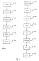
- step 103 an HF hume treatment is performed to remove native oxide having formed on the Si surface by the oxygen in the ambient air.
- an HF spin with a diluted solution may be used.
- the F in the HF hume or HF water solution also bonds to the Si on the surface and achieves a Si-surface passivation by forming Si-F bonds, which prevent surface oxidation.
- Evaporation of the adhesion metal, diffusion barrier metal and Au/Sn stack is performed in step 104. This step is further detailed in figure 3. After evaporation the wafer is taped on the backside with an UV curable tape and sawed in step 105 and finally the individual dies are soldered to respective package flanges.
- a thinner metal stack is preferable when the wafer thickness is around or below 60 ⁇ m.
- the thinner metal stack of 6 ⁇ m requires a better flatness of the flange.
- Such a thinner metal stack may be constituted by for instance 100nm Ti / 100nm Pt / 3400nm Au / 1900 nm Sn / 700 nm Au, in order from the Si surface and out.
Landscapes
- Die Bonding (AREA)
- Cooling Or The Like Of Semiconductors Or Solid State Devices (AREA)
Claims (41)
- Verfahren zum Befestigen von Si-Schaltungschips (503) an Kühlkörpern (502), wobei jeder der Chips (503) von einem Wafer (401) abgesägt wird, umfassend die folgenden Schritte:- Reduzieren der Dicke des Wafers (401) durch mechanisches Schleifen,- Anwenden einer isotropen naßchemischen Ätzung auf dem Wafer (401), um Kristalldefekte zu eliminieren,- Aufdampfen von Haftungs-(402) und Diffusions-(403)-Barrieremetallen auf die Rückseite des Wafers (401),- Aufdampfen von Au (404, 406) und Sn (405) auf die Rückseite des Wafers (401), wobei der Gewichtsanteil von Au (404, 406) größer oder gleich 85% ist,- Zersägen des Wafers (401) in die Schaltungschips (503) und- Löten jedes der Schaltungschips (503) an einen jeweiligen Kühlkörper (502).
- Verfahren nach Anspruch 1, wobei- der Kühlkörper (502) ein Flansch eines integrierten Schaltungsbausteins (501) ist.
- Verfahren nach Anspruch 1, wobei- der Kühlkörper (502) ein Kühlkörper auf einem HF-Leistungsmodul oder einer gedruckten Leiterplatte ist.
- Verfahren nach einem der Ansprüche 1-3, wobei der Schaltungschip (503) ein integrierter Schaltungschip, ein Leistungstransistor oder ein Kondensator ist, und wobei einer oder mehrere der Schaltungschips (503) an einen jeweiligen Flansch (502) des Bausteins (501) gelötet sind.
- Verfahren nach einem der Ansprüche 1-4, wobei die isotrope naßchemische Ätzung eine isotrope Aufschleuderätzung ist.
- Verfahren nach Anspruch 1, umfassend den folgenden Schritt:- Anwenden einer aufrauhenden Aufschleuderätzung auf die Si-Oberfläche nach der isotropen naßchemischen Ätzung zum Aufrauhen der Si-Oberfläche.
- Verfahren nach Anspruch 1, wobei der Schritt des Anwendens einer isotropen naßchemischen Ätzung mindestens 25 µm der Waferrückseite entfernt.
- Verfahren nach Anspruch 1, wobei- der Kühlkörper (502) reines Cu oder eine Legierung aus Cu und Zr oder ein CPC-Material oder ein PCM-Material ist.
- Verfahren nach Anspruch 1, wobei- der Schritt des Aufdampfens von Au (404, 406) und Sn (405) auf die Rückseite des Wafers (401) durchgeführt wird durch Aufdampfen einer ersten Au-Schicht (404), einer Sn-Schicht (405) und einer zweiten Au-Schicht (406).
- Verfahrensschritt nach Anspruch 1, wobei- der Schritt des Aufdampfens von Au (404, 406) und Sn (405) auf die Rückseite des Wafers (401) durchgeführt wird durch Aufdampfen einer ersten Au-Schicht (404) und einer Sn-Schicht (405).
- Verfahren nach Anspruch 10, wobei- die erste Au-Schicht (404) so ausgebildet wird, daß mindestens ein Teil der ersten Au-Schicht (404), neben der Diffusionsbarrieremetallschicht (403) angeordnet, während des Schritts des Lötens des Schaltungschips (503) an den Kühlkörper (502) seinen festen Zustand beibehält.
- Verfahren nach Anspruch 1, wobei- der Kühlkörper (502) eine Schicht aus plattiertem Au umfaßt, die zusammen mit den Au-(404, 406) und Sn-(405)-Schichten auf dem Wafer (401) während des Schritts des Lötens ein an Au reicheres Lot bildet als die eutektische Zusammensetzung aus Au und Sn, mit 80 Gew.-% Au und 20 Gew.-% Sn.
- Verfahren nach Anspruch 12 wobei- das an Au reichere Lot zwischen 86 und 89 Gewichtsprozent Au umfaßt.
- Verfahren nach Anspruch 1, wobei- der Schritt des Aufdampfens von Haftungs-(402)-und Diffusions-(403)-Barrieremetallen das Aufdampfen einer Ti-Schicht (402) und das Aufdampfen einer Pt-Schicht (403) auf der Rückseite des Wafers (401) umfaßt.
- Verfahren nach Anspruch 6, umfassend den folgenden Schritt:- Anwenden einer Abrundungs-Aufschleuderätzung nach der Aufrauhungsätzung, um scharfe einspringende Spitzen zu eliminieren.
- Verfahren zum Herstellen eines an einem Kühlkörper (502) zu befestigenden Si-Schaltungschips (503), wobei der Schaltungschip (503) von einem Wafer (401) abgesägt wird, umfassend die folgenden Schritte:- Reduzieren der Dicke des Wafers (401) durch mechanisches Schleifen,- Anwenden einer isotropen naßchemischen Ätzung auf dem Wafer (401), um Kristalldefekte zu eliminieren,- Aufdampfen von Haftungs-(402) und Diffusions-(403)-Barrieremetallen auf die Rückseite des Wafers (401),- Aufdampfen von Au (404, 406) und Sn (405) auf die Rückseite des Wafers (401), wobei der Gewichtsanteil von Au größer oder gleich 85% ist und- Zersägen des Wafers (401) in die Schaltungschips (503).
- Verfahren nach Anspruch 16, wobei- der Kühlkörper (502) ein Flansch eines Schaltungsbausteins (501) ist.
- Verfahren nach Anspruch 16, wobei- der Kühlkörper (502) ein Kühlkörper auf einem HF-Leistungsmodul oder einer gedruckten Leiterplatte ist.
- Verfahren nach Anspruch 16, wobei der Schaltungschip (503) ein integrierter Schaltungschip, ein Leistungstransistor oder ein Kondensator ist, und wobei einer oder mehrere der Schaltungschips an einen jeweiligen Flansch des Bausteins gelötet sind.
- Verfahren nach Anspruch 16, wobei die isotrope naßchemische Ätzung eine isotrope Aufschleuderätzung ist.
- Verfahren nach Anspruch 16, umfassend den folgenden Schritt:- Anwenden einer aufrauhenden Ätzung auf das Si nach der isotropen naßchemischen Ätzung zum Aufrauhen der Si-Oberfläche.
- Verfahren nach Anspruch 16, wobei- der Schritt des Aufdampfens von Au (404, 406) und Sn (405) auf die Rückseite des Wafers (401) durchgeführt wird durch Aufdampfen einer ersten Au-Schicht (404), einer Sn-Schicht (405) und einer zweiten Au-Schicht (406).
- Verfahren nach Anspruch 22, wobei- die erste Au-Schicht (404) so ausgebildet wird, daß mindestens ein Teil der ersten Au-Schicht (404), neben der Pt-Schicht (403) angeordnet, während des Schritts des Lötens des Schaltungschips (503) an den Kühlkörper (502) ihren festen Zustand beibehält.
- Verfahren nach Anspruch 16, wobei- der Flansch (502) eine Schicht aus plattiertem Au umfaßt, die zusammen mit den Au-(404, 406) und Sn-(405)-Schichten auf dem Chip während des Schritts des Lötens ein an Au reicheres Lot bildet.
- Verfahren nach Anspruch 24, wobei- das an Au reichere Lot zwischen 86 und 89 Gewichtsprozent Au umfaßt.
- Verfahren nach Anspruch 16, wobei- der Schritt des Aufdampfens von Haftungs-(402)- und Diffusions-(403)-Barrieremetallen das Aufdampfen einer Ti-Schicht (402) und das Aufdampfen einer Pt-Schicht (403) auf der Rückseite des Wafers (401) umfaßt.
- Verfahren nach Anspruch 21, umfassend den folgenden Schritt:- Anwenden einer Abrundungsätzung nach der Aufrauhungsätzung, um scharfe einspringende Spitzen zu eliminieren.
- Si-Schaltungschip, hergestellt nach einem der Ansprüche 16 bis 27.
- Si-Schaltungschip, umfassend:- eine Schicht aus Haftungs-(402)- und Diffusions-(403)-Barrieremetallen auf einer Rückseite des an einem Kühlkörper (502) anzubringenden Chips (503),- einen Stapel von abwechselnden Schichten aus Au (404, 406) und Sn (405), wobei eine erste Schicht (404) in dem Stapel neben der Schicht aus Diffusionsbarrieremetall (403), eine Au-Schicht (404) ist und die Endschicht in dem Stapel eine Au-Schicht (406) ist,dadurch gekennzeichnet, daß- der Gewichtsprozentsatz von Au zu Sn in dem Stapel größer oder gleich 85% ist.
- Schaltungschip nach Anspruch 29, wobei der Schaltungschip ein integrierter Schaltungschip, ein Leistungstransistor, ein Kondensator, eine Induktionsspule, eine Diode oder ein Widerstand ist.
- Schaltungschip nach Anspruch 29, wobei- die Schicht aus Haftungs-(402)- und Diffusions-(403)-Barrieremetallen eine erste Schicht aus Ti (402) und eine zweite Schicht aus Pt (403) umfaßt.
- Schaltungschip nach Anspruch 29, wobei- der Schaltungschip weniger als 150 µm dick ist, bevorzugt 40 µm bis 80 µm.
- Schaltungschip nach Anspruch 29, wobei- die Rückseite des Schaltungschips ein Minimum an oder keine Kristalldefekte umfaßt.
- Schaltungschip nach Anspruch 29, wobei- die erste Schicht aus Au (404) in dem Stapel so dick ist, daß zumindest ein Teil der Schicht (404), neben dem Diffusionsbarrieremetall (403), während des Lötens des Chips an einen Kühlkörper (502) seinen festen Zustand beibehält.
- Schaltungschip nach Anspruch 34, wobei- die erste Schicht aus Au (404) 3 µm bis 6 µm, bevorzugt 5 µm dick ist für eine Chipdicke über 60 µm und 3 µm für eine Chipdicke unter 60 µm.
- Schaltungschip nach Anspruch 29, wobei- die Endschicht aus Au (406) in dem Stapel dick genug ist, um eine glatte Oberfläche zu erzeugen, um das Ablösen vom Sägeband zu erleichtern.
- Schaltungschip nach Anspruch 36, wobei- die Endschicht aus Au (406) zwischen 0,5 und 1,0 µm dick ist.
- Schaltungschip nach Anspruch 29, wobei- der Stapel aus abwechselnden Schichten aus Au (404, 406) und Sn (405) 3 Schichten umfaßt, nämlich eine erste Schicht aus Au (404), eine Schicht aus Sn (405) und eine Endschicht aus Au (406) .
- Schaltungsbaustein, umfassend einen Flansch (502) und eine integrierte Si-Schaltung (503) nach einem der Ansprüche 29 bis 38, wobei der Flansch (502) aus einer Legierung aus Cu und Zr oder einem CPC-Material oder einem PCM-Material hergestellt ist.
- Leistungsmodul, umfassend einen Kühlkörper (502) und eine integrierte Si-Schaltung (503) nach einem der Ansprüche 29 bis 38, wobei der Kühlkörper (502) aus einer Legierung aus Cu und Zr oder einem CPC-Material oder einem PCM-Material hergestellt ist.
- Schaltungsbaustein nach Anspruch 39, wobei- die Beziehung zwischen Au (404, 406) und Sn (405) in dem Stapel aus Au und Sn durch die Anforderung bestimmt wird, daß nach dem Löten des Schaltungschips (503) an den Flansch (502) auf dem integrierten Schaltungspaket (501) der Gewichtsprozentsatz von Au in dem Stapel zwischen 86% und 89% liegen sollte.
Priority Applications (5)
| Application Number | Priority Date | Filing Date | Title |
|---|---|---|---|
| DE602004010061T DE602004010061T2 (de) | 2004-03-09 | 2004-03-09 | Hochzuverlässige, kostengünstige und thermisch verbesserte Halbleiterchip-Befestigungstechnologie mit AuSn |
| EP04445024A EP1575089B1 (de) | 2004-03-09 | 2004-03-09 | Hochzuverlässige, kostengünstige und thermisch verbesserte Halbleiterchip-Befestigungstechnologie mit AuSn |
| JP2007502765A JP4700681B2 (ja) | 2004-03-09 | 2005-03-07 | Si回路ダイ、Si回路ダイを製作する方法およびSi回路ダイをヒートシンクに取り付ける方法並びに回路パッケージと電力モジュール |
| PCT/SE2005/000331 WO2005086220A1 (en) | 2004-03-09 | 2005-03-07 | Highly reliable, cost effective and thermally enhanced ausn die-attach technology |
| US11/530,276 US7608485B2 (en) | 2004-03-09 | 2006-09-08 | Highly reliable, cost effective and thermally enhanced AuSn die-attach technology |
Applications Claiming Priority (1)
| Application Number | Priority Date | Filing Date | Title |
|---|---|---|---|
| EP04445024A EP1575089B1 (de) | 2004-03-09 | 2004-03-09 | Hochzuverlässige, kostengünstige und thermisch verbesserte Halbleiterchip-Befestigungstechnologie mit AuSn |
Publications (2)
| Publication Number | Publication Date |
|---|---|
| EP1575089A1 EP1575089A1 (de) | 2005-09-14 |
| EP1575089B1 true EP1575089B1 (de) | 2007-11-14 |
Family
ID=34814471
Family Applications (1)
| Application Number | Title | Priority Date | Filing Date |
|---|---|---|---|
| EP04445024A Expired - Lifetime EP1575089B1 (de) | 2004-03-09 | 2004-03-09 | Hochzuverlässige, kostengünstige und thermisch verbesserte Halbleiterchip-Befestigungstechnologie mit AuSn |
Country Status (5)
| Country | Link |
|---|---|
| US (1) | US7608485B2 (de) |
| EP (1) | EP1575089B1 (de) |
| JP (1) | JP4700681B2 (de) |
| DE (1) | DE602004010061T2 (de) |
| WO (1) | WO2005086220A1 (de) |
Families Citing this family (14)
| Publication number | Priority date | Publication date | Assignee | Title |
|---|---|---|---|---|
| US7327029B2 (en) * | 2005-09-27 | 2008-02-05 | Agere Systems, Inc. | Integrated circuit device incorporating metallurigical bond to enhance thermal conduction to a heat sink |
| JP2009054892A (ja) | 2007-08-28 | 2009-03-12 | Panasonic Electric Works Co Ltd | Ledチップの実装方法 |
| US8828804B2 (en) * | 2008-04-30 | 2014-09-09 | Infineon Technologies Ag | Semiconductor device and method |
| US7754533B2 (en) * | 2008-08-28 | 2010-07-13 | Infineon Technologies Ag | Method of manufacturing a semiconductor device |
| US8637379B2 (en) * | 2009-10-08 | 2014-01-28 | Infineon Technologies Ag | Device including a semiconductor chip and a carrier and fabrication method |
| US8994182B2 (en) | 2012-12-21 | 2015-03-31 | Cree, Inc. | Dielectric solder barrier for semiconductor devices |
| US8970010B2 (en) | 2013-03-15 | 2015-03-03 | Cree, Inc. | Wafer-level die attach metallization |
| JP5877487B1 (ja) * | 2014-12-26 | 2016-03-08 | パナソニックIpマネジメント株式会社 | 発光装置 |
| US9893027B2 (en) | 2016-04-07 | 2018-02-13 | Nxp Usa, Inc. | Pre-plated substrate for die attachment |
| CA3046489A1 (en) | 2016-12-07 | 2018-06-14 | Progenity Inc. | Gastrointestinal tract detection methods, devices and systems |
| US10980739B2 (en) | 2016-12-14 | 2021-04-20 | Progenity, Inc. | Treatment of a disease of the gastrointestinal tract with a chemokine/chemokine receptor inhibitor |
| US20240252795A1 (en) | 2018-11-19 | 2024-08-01 | Biora Therapeutics, Inc. | Ingestible device for delivery of therapeutic agent to the gastrointestinal tract |
| CN121197633A (zh) | 2019-12-13 | 2025-12-26 | 比特比德科有限责任公司 | 用于将治疗剂递送至胃肠道的可摄取装置 |
| CN114171422B (zh) * | 2022-02-11 | 2022-06-03 | 浙江里阳半导体有限公司 | 半导体器件的制造方法及其蒸镀缺陷的检测方法 |
Family Cites Families (33)
| Publication number | Priority date | Publication date | Assignee | Title |
|---|---|---|---|---|
| US3648357A (en) * | 1969-07-31 | 1972-03-14 | Gen Dynamics Corp | Method for sealing microelectronic device packages |
| JPS556839A (en) * | 1978-06-28 | 1980-01-18 | Nec Corp | Semiconductor device |
| JPS5837713B2 (ja) * | 1978-12-01 | 1983-08-18 | 富士通株式会社 | 半導体レ−ザ−装置の製造方法 |
| US4518112A (en) * | 1982-12-30 | 1985-05-21 | International Business Machines Corporation | Process for controlled braze joining of electronic packaging elements |
| JPS6156422A (ja) * | 1984-08-28 | 1986-03-22 | Nec Corp | 半導体装置 |
| JPS6223118A (ja) * | 1985-07-24 | 1987-01-31 | Hitachi Ltd | 半導体装置 |
| US4875617A (en) * | 1987-01-20 | 1989-10-24 | Citowsky Elya L | Gold-tin eutectic lead bonding method and structure |
| JPH0793329B2 (ja) * | 1987-03-10 | 1995-10-09 | 日本鉱業株式会社 | 半導体ペレツトの固定方法 |
| GB2221570B (en) * | 1988-08-04 | 1992-02-12 | Stc Plc | Bonding a semiconductor to a substrate |
| DE4025622A1 (de) * | 1990-08-13 | 1992-02-20 | Siemens Ag | Anschlusskontakthoecker und verfahren zu dessen herstellung |
| JPH0665376B2 (ja) * | 1990-10-19 | 1994-08-24 | 日本碍子株式会社 | セラミック粒の製造方法 |
| JP2605502B2 (ja) * | 1991-05-14 | 1997-04-30 | 三菱電機株式会社 | パッケージ |
| US5353193A (en) * | 1993-02-26 | 1994-10-04 | Lsi Logic Corporation | High power dissipating packages with matched heatspreader heatsink assemblies |
| JPH06349866A (ja) * | 1993-06-10 | 1994-12-22 | Sumitomo Electric Ind Ltd | 半導体ウェハ及び半導体素子のダイボンディング方法 |
| US5384690A (en) * | 1993-07-27 | 1995-01-24 | International Business Machines Corporation | Flex laminate package for a parallel processor |
| JPH07130685A (ja) * | 1993-11-05 | 1995-05-19 | Sumitomo Electric Ind Ltd | 半導体ウェーハの製造方法 |
| GB2300375B (en) * | 1994-08-01 | 1998-02-25 | Nippon Denso Co | Bonding method for electric element |
| JPH09283909A (ja) * | 1996-04-19 | 1997-10-31 | Hitachi Ltd | 電子回路装置およびその製造方法 |
| US6027957A (en) * | 1996-06-27 | 2000-02-22 | University Of Maryland | Controlled solder interdiffusion for high power semiconductor laser diode die bonding |
| US5847929A (en) * | 1996-06-28 | 1998-12-08 | International Business Machines Corporation | Attaching heat sinks directly to flip chips and ceramic chip carriers |
| JPH1079471A (ja) * | 1996-09-05 | 1998-03-24 | Hitachi Ltd | 半導体装置、その製造方法及びフレキシブルカード |
| JP3796016B2 (ja) * | 1997-03-28 | 2006-07-12 | 三洋電機株式会社 | 半導体装置 |
| JPH11204884A (ja) * | 1998-01-07 | 1999-07-30 | Mitsubishi Electric Corp | ハンダ形成方法 |
| TW380284B (en) * | 1998-09-09 | 2000-01-21 | Promos Technologies Inc | Method for improving etching uniformity during a wet etching process |
| US6180505B1 (en) * | 1999-01-07 | 2001-01-30 | International Business Machines Corporation | Process for forming a copper-containing film |
| JP2002151541A (ja) * | 2000-11-15 | 2002-05-24 | Hitachi Ltd | 電子部品 |
| JP4497737B2 (ja) * | 2001-03-12 | 2010-07-07 | 株式会社ルネサステクノロジ | 半導体装置の製造方法 |
| JP2003037231A (ja) * | 2001-07-23 | 2003-02-07 | Ibiden Co Ltd | モジュール用基板 |
| JP2003068751A (ja) * | 2001-08-27 | 2003-03-07 | Nec Yamagata Ltd | 半導体装置及びその製造方法 |
| JP4514400B2 (ja) * | 2001-09-27 | 2010-07-28 | 古河電気工業株式会社 | 部材の接合方法、その方法で得られた接合部材 |
| JP3816821B2 (ja) * | 2002-03-20 | 2006-08-30 | 株式会社住友金属エレクトロデバイス | 高周波用パワーモジュール基板及びその製造方法 |
| US6660548B2 (en) * | 2002-03-27 | 2003-12-09 | Intel Corporation | Packaging of multiple active optical devices |
| US6833289B2 (en) * | 2003-05-12 | 2004-12-21 | Intel Corporation | Fluxless die-to-heat spreader bonding using thermal interface material |
-
2004
- 2004-03-09 EP EP04445024A patent/EP1575089B1/de not_active Expired - Lifetime
- 2004-03-09 DE DE602004010061T patent/DE602004010061T2/de not_active Expired - Lifetime
-
2005
- 2005-03-07 JP JP2007502765A patent/JP4700681B2/ja not_active Expired - Fee Related
- 2005-03-07 WO PCT/SE2005/000331 patent/WO2005086220A1/en not_active Ceased
-
2006
- 2006-09-08 US US11/530,276 patent/US7608485B2/en not_active Expired - Fee Related
Also Published As
| Publication number | Publication date |
|---|---|
| US20070181987A1 (en) | 2007-08-09 |
| EP1575089A1 (de) | 2005-09-14 |
| WO2005086220A1 (en) | 2005-09-15 |
| DE602004010061D1 (de) | 2007-12-27 |
| JP2007528601A (ja) | 2007-10-11 |
| JP4700681B2 (ja) | 2011-06-15 |
| US7608485B2 (en) | 2009-10-27 |
| DE602004010061T2 (de) | 2008-09-11 |
Similar Documents
| Publication | Publication Date | Title |
|---|---|---|
| KR100940164B1 (ko) | 서브마운트 및 반도체 장치 | |
| EP1575089B1 (de) | Hochzuverlässige, kostengünstige und thermisch verbesserte Halbleiterchip-Befestigungstechnologie mit AuSn | |
| JP6499545B2 (ja) | 金属セラミック接合基板及び、その製造方法 | |
| KR20050061452A (ko) | 서브 마운트 및 반도체 장치 | |
| TW201325330A (zh) | 配線基板及其製造方法以及半導體裝置 | |
| KR20170044105A (ko) | 접합체, 히트 싱크가 부착된 파워 모듈용 기판, 히트 싱크, 접합체의 제조 방법, 히트 싱크가 부착된 파워 모듈용 기판의 제조 방법, 및 히트 싱크의 제조 방법 | |
| CN1194409C (zh) | 电路板及其制作方法和高输出模块 | |
| US8084861B2 (en) | Connection structure semiconductor chip and electronic component including the connection structure and methods for producing the connection structure | |
| CN104798185B (zh) | Au系钎料模片接合半导体装置及其制造方法 | |
| JP5640569B2 (ja) | パワーモジュール用基板の製造方法 | |
| JP4409041B2 (ja) | サブマウント材 | |
| WO2025060485A1 (zh) | 一种功率模组及其制作方法、功率设备 | |
| JP6221590B2 (ja) | 絶縁基板と冷却器の接合構造体、その製造方法、パワー半導体モジュール、及びその製造方法 | |
| TWI446577B (zh) | Led晶圓之接合方法、led晶粒之製造方法及led晶圓與基體之接合結構 | |
| JP2025504702A (ja) | 高信頼性を有するパターン形成されたメタライゼーションを備える半導体チップ、及び同半導体チップを製造する方法 | |
| JP7179550B2 (ja) | セラミックス回路基板およびそれを用いた半導体装置 | |
| KR101878492B1 (ko) | 파워 모듈용 기판의 제조 방법, 파워 모듈용 기판, 히트싱크가 부착된 파워 모듈용 기판 및 파워 모듈 | |
| US20250226284A1 (en) | Thermal mismatch reduction in semiconductor device modules | |
| JP2014086607A (ja) | Au系はんだダイアタッチメント半導体装置及びその製造方法 | |
| KR101726003B1 (ko) | 파워 모듈용 기판, 히트 싱크 부착 파워 모듈용 기판, 파워 모듈 및 파워 모듈용 기판의 제조 방법 | |
| JP4409553B2 (ja) | サブマウント材用基板の製造方法 | |
| Wu et al. | High temperature Ag-In joints between Si chips and aluminum | |
| WO2025134898A1 (ja) | セラミックス回路基板及びその製造方法 | |
| KR101711217B1 (ko) | 파워 모듈용 기판, 히트 싱크 부착 파워 모듈용 기판, 파워 모듈 및 파워 모듈용 기판의 제조 방법 | |
| CN121420693A (zh) | 陶瓷电路基板及其制造方法 |
Legal Events
| Date | Code | Title | Description |
|---|---|---|---|
| PUAI | Public reference made under article 153(3) epc to a published international application that has entered the european phase |
Free format text: ORIGINAL CODE: 0009012 |
|
| AK | Designated contracting states |
Kind code of ref document: A1 Designated state(s): AT BE BG CH CY CZ DE DK EE ES FI FR GB GR HU IE IT LI LU MC NL PL PT RO SE SI SK TR |
|
| AX | Request for extension of the european patent |
Extension state: AL LT LV MK |
|
| 17P | Request for examination filed |
Effective date: 20051013 |
|
| AKX | Designation fees paid |
Designated state(s): DE FR GB IT NL |
|
| GRAP | Despatch of communication of intention to grant a patent |
Free format text: ORIGINAL CODE: EPIDOSNIGR1 |
|
| RIC1 | Information provided on ipc code assigned before grant |
Ipc: H01L 21/60 20060101ALI20070523BHEP Ipc: H01L 21/78 20060101ALI20070523BHEP Ipc: H01L 21/306 20060101ALI20070523BHEP Ipc: H01L 21/58 20060101ALI20070523BHEP Ipc: H01L 23/373 20060101AFI20070523BHEP Ipc: H01L 23/492 20060101ALI20070523BHEP |
|
| GRAS | Grant fee paid |
Free format text: ORIGINAL CODE: EPIDOSNIGR3 |
|
| GRAA | (expected) grant |
Free format text: ORIGINAL CODE: 0009210 |
|
| AK | Designated contracting states |
Kind code of ref document: B1 Designated state(s): DE FR GB IT NL |
|
| REG | Reference to a national code |
Ref country code: GB Ref legal event code: FG4D |
|
| REF | Corresponds to: |
Ref document number: 602004010061 Country of ref document: DE Date of ref document: 20071227 Kind code of ref document: P |
|
| PG25 | Lapsed in a contracting state [announced via postgrant information from national office to epo] |
Ref country code: NL Free format text: LAPSE BECAUSE OF FAILURE TO SUBMIT A TRANSLATION OF THE DESCRIPTION OR TO PAY THE FEE WITHIN THE PRESCRIBED TIME-LIMIT Effective date: 20071114 |
|
| NLV1 | Nl: lapsed or annulled due to failure to fulfill the requirements of art. 29p and 29m of the patents act | ||
| EN | Fr: translation not filed | ||
| PLBE | No opposition filed within time limit |
Free format text: ORIGINAL CODE: 0009261 |
|
| STAA | Information on the status of an ep patent application or granted ep patent |
Free format text: STATUS: NO OPPOSITION FILED WITHIN TIME LIMIT |
|
| 26N | No opposition filed |
Effective date: 20080815 |
|
| PG25 | Lapsed in a contracting state [announced via postgrant information from national office to epo] |
Ref country code: FR Free format text: LAPSE BECAUSE OF FAILURE TO SUBMIT A TRANSLATION OF THE DESCRIPTION OR TO PAY THE FEE WITHIN THE PRESCRIBED TIME-LIMIT Effective date: 20080829 |
|
| GBPC | Gb: european patent ceased through non-payment of renewal fee |
Effective date: 20080309 |
|
| PG25 | Lapsed in a contracting state [announced via postgrant information from national office to epo] |
Ref country code: GB Free format text: LAPSE BECAUSE OF NON-PAYMENT OF DUE FEES Effective date: 20080309 |
|
| PG25 | Lapsed in a contracting state [announced via postgrant information from national office to epo] |
Ref country code: IT Free format text: LAPSE BECAUSE OF NON-PAYMENT OF DUE FEES Effective date: 20080331 |
|
| PGFP | Annual fee paid to national office [announced via postgrant information from national office to epo] |
Ref country code: DE Payment date: 20180518 Year of fee payment: 15 |
|
| REG | Reference to a national code |
Ref country code: DE Ref legal event code: R119 Ref document number: 602004010061 Country of ref document: DE |
|
| PG25 | Lapsed in a contracting state [announced via postgrant information from national office to epo] |
Ref country code: DE Free format text: LAPSE BECAUSE OF NON-PAYMENT OF DUE FEES Effective date: 20191001 |