EP1573790B1 - Semiconductor devices with reduced active region defects and unique contacting schemes - Google Patents
Semiconductor devices with reduced active region defects and unique contacting schemes Download PDFInfo
- Publication number
- EP1573790B1 EP1573790B1 EP03808419A EP03808419A EP1573790B1 EP 1573790 B1 EP1573790 B1 EP 1573790B1 EP 03808419 A EP03808419 A EP 03808419A EP 03808419 A EP03808419 A EP 03808419A EP 1573790 B1 EP1573790 B1 EP 1573790B1
- Authority
- EP
- European Patent Office
- Prior art keywords
- region
- opening
- cladding
- regions
- layer
- Prior art date
- Legal status (The legal status is an assumption and is not a legal conclusion. Google has not performed a legal analysis and makes no representation as to the accuracy of the status listed.)
- Expired - Lifetime
Links
- 230000007547 defect Effects 0.000 title claims description 58
- 239000004065 semiconductor Substances 0.000 title claims description 25
- 230000002829 reductive effect Effects 0.000 title claims description 7
- 238000000034 method Methods 0.000 claims description 73
- 238000005253 cladding Methods 0.000 claims description 67
- 239000000463 material Substances 0.000 claims description 50
- 239000000758 substrate Substances 0.000 claims description 42
- 229910006990 Si1-xGex Inorganic materials 0.000 claims description 37
- 229910007020 Si1−xGex Inorganic materials 0.000 claims description 37
- 239000013078 crystal Substances 0.000 claims description 11
- 230000000903 blocking effect Effects 0.000 claims description 10
- 238000004519 manufacturing process Methods 0.000 claims description 10
- 238000005530 etching Methods 0.000 claims description 5
- 239000010410 layer Substances 0.000 description 109
- 229910052751 metal Inorganic materials 0.000 description 34
- 239000002184 metal Substances 0.000 description 34
- 238000013461 design Methods 0.000 description 23
- 230000008569 process Effects 0.000 description 22
- 238000004088 simulation Methods 0.000 description 22
- 238000010521 absorption reaction Methods 0.000 description 20
- 238000006862 quantum yield reaction Methods 0.000 description 20
- 229910000577 Silicon-germanium Inorganic materials 0.000 description 17
- 230000003287 optical effect Effects 0.000 description 14
- 239000000969 carrier Substances 0.000 description 12
- 238000009792 diffusion process Methods 0.000 description 12
- 238000004891 communication Methods 0.000 description 11
- 230000004044 response Effects 0.000 description 11
- VYPSYNLAJGMNEJ-UHFFFAOYSA-N Silicium dioxide Chemical compound O=[Si]=O VYPSYNLAJGMNEJ-UHFFFAOYSA-N 0.000 description 10
- 238000012545 processing Methods 0.000 description 10
- 229910052732 germanium Inorganic materials 0.000 description 9
- 238000013459 approach Methods 0.000 description 7
- 230000015572 biosynthetic process Effects 0.000 description 7
- 239000003989 dielectric material Substances 0.000 description 7
- 229910052710 silicon Inorganic materials 0.000 description 7
- 239000012212 insulator Substances 0.000 description 6
- 230000000670 limiting effect Effects 0.000 description 6
- 239000000203 mixture Substances 0.000 description 6
- 229910021421 monocrystalline silicon Inorganic materials 0.000 description 6
- 239000002019 doping agent Substances 0.000 description 5
- 230000005684 electric field Effects 0.000 description 5
- 239000000835 fiber Substances 0.000 description 5
- 239000007943 implant Substances 0.000 description 5
- 230000001965 increasing effect Effects 0.000 description 5
- 230000035515 penetration Effects 0.000 description 5
- 239000000377 silicon dioxide Substances 0.000 description 5
- 208000012868 Overgrowth Diseases 0.000 description 4
- 230000004888 barrier function Effects 0.000 description 4
- 230000010354 integration Effects 0.000 description 4
- 238000001459 lithography Methods 0.000 description 4
- 235000012239 silicon dioxide Nutrition 0.000 description 4
- 229910052581 Si3N4 Inorganic materials 0.000 description 3
- 239000006096 absorbing agent Substances 0.000 description 3
- 238000000137 annealing Methods 0.000 description 3
- 230000008901 benefit Effects 0.000 description 3
- 230000007423 decrease Effects 0.000 description 3
- 230000002950 deficient Effects 0.000 description 3
- 238000001514 detection method Methods 0.000 description 3
- 230000002708 enhancing effect Effects 0.000 description 3
- 238000011065 in-situ storage Methods 0.000 description 3
- 238000005468 ion implantation Methods 0.000 description 3
- 230000031700 light absorption Effects 0.000 description 3
- 230000006911 nucleation Effects 0.000 description 3
- 238000010899 nucleation Methods 0.000 description 3
- 230000005693 optoelectronics Effects 0.000 description 3
- 230000000149 penetrating effect Effects 0.000 description 3
- 238000005498 polishing Methods 0.000 description 3
- XKRFYHLGVUSROY-UHFFFAOYSA-N Argon Chemical compound [Ar] XKRFYHLGVUSROY-UHFFFAOYSA-N 0.000 description 2
- NBIIXXVUZAFLBC-UHFFFAOYSA-N Phosphoric acid Chemical compound OP(O)(O)=O NBIIXXVUZAFLBC-UHFFFAOYSA-N 0.000 description 2
- BOTDANWDWHJENH-UHFFFAOYSA-N Tetraethyl orthosilicate Chemical compound CCO[Si](OCC)(OCC)OCC BOTDANWDWHJENH-UHFFFAOYSA-N 0.000 description 2
- 229910052786 argon Inorganic materials 0.000 description 2
- 238000010420 art technique Methods 0.000 description 2
- 238000000576 coating method Methods 0.000 description 2
- 150000001875 compounds Chemical class 0.000 description 2
- 238000011109 contamination Methods 0.000 description 2
- 230000003247 decreasing effect Effects 0.000 description 2
- 238000000151 deposition Methods 0.000 description 2
- 230000008021 deposition Effects 0.000 description 2
- 230000000873 masking effect Effects 0.000 description 2
- 150000002739 metals Chemical class 0.000 description 2
- 239000013307 optical fiber Substances 0.000 description 2
- 238000005215 recombination Methods 0.000 description 2
- 230000009467 reduction Effects 0.000 description 2
- 230000002441 reversible effect Effects 0.000 description 2
- 230000035945 sensitivity Effects 0.000 description 2
- HQVNEWCFYHHQES-UHFFFAOYSA-N silicon nitride Chemical compound N12[Si]34N5[Si]62N3[Si]51N64 HQVNEWCFYHHQES-UHFFFAOYSA-N 0.000 description 2
- 239000002356 single layer Substances 0.000 description 2
- XPDWGBQVDMORPB-UHFFFAOYSA-N Fluoroform Chemical compound FC(F)F XPDWGBQVDMORPB-UHFFFAOYSA-N 0.000 description 1
- 229910001218 Gallium arsenide Inorganic materials 0.000 description 1
- XUIMIQQOPSSXEZ-UHFFFAOYSA-N Silicon Chemical compound [Si] XUIMIQQOPSSXEZ-UHFFFAOYSA-N 0.000 description 1
- 230000002411 adverse Effects 0.000 description 1
- 229910045601 alloy Inorganic materials 0.000 description 1
- 239000000956 alloy Substances 0.000 description 1
- PNEYBMLMFCGWSK-UHFFFAOYSA-N aluminium oxide Inorganic materials [O-2].[O-2].[O-2].[Al+3].[Al+3] PNEYBMLMFCGWSK-UHFFFAOYSA-N 0.000 description 1
- 229910000147 aluminium phosphate Inorganic materials 0.000 description 1
- 238000004364 calculation method Methods 0.000 description 1
- 239000011248 coating agent Substances 0.000 description 1
- 229910052681 coesite Inorganic materials 0.000 description 1
- 239000012141 concentrate Substances 0.000 description 1
- 229910052593 corundum Inorganic materials 0.000 description 1
- 229910052906 cristobalite Inorganic materials 0.000 description 1
- 125000004122 cyclic group Chemical group 0.000 description 1
- 238000009826 distribution Methods 0.000 description 1
- 230000000694 effects Effects 0.000 description 1
- 239000007789 gas Substances 0.000 description 1
- GNPVGFCGXDBREM-UHFFFAOYSA-N germanium atom Chemical compound [Ge] GNPVGFCGXDBREM-UHFFFAOYSA-N 0.000 description 1
- 230000003116 impacting effect Effects 0.000 description 1
- 238000002513 implantation Methods 0.000 description 1
- 230000006872 improvement Effects 0.000 description 1
- 230000007246 mechanism Effects 0.000 description 1
- 230000008018 melting Effects 0.000 description 1
- 238000002844 melting Methods 0.000 description 1
- 238000001465 metallisation Methods 0.000 description 1
- 230000007935 neutral effect Effects 0.000 description 1
- 238000005457 optimization Methods 0.000 description 1
- 230000003071 parasitic effect Effects 0.000 description 1
- 230000036961 partial effect Effects 0.000 description 1
- 229910021420 polycrystalline silicon Inorganic materials 0.000 description 1
- 229920005591 polysilicon Polymers 0.000 description 1
- 230000005855 radiation Effects 0.000 description 1
- 230000006798 recombination Effects 0.000 description 1
- 229920006395 saturated elastomer Polymers 0.000 description 1
- 239000010703 silicon Substances 0.000 description 1
- 229910052682 stishovite Inorganic materials 0.000 description 1
- 239000000126 substance Substances 0.000 description 1
- 239000002344 surface layer Substances 0.000 description 1
- 229910052905 tridymite Inorganic materials 0.000 description 1
- 229910001845 yogo sapphire Inorganic materials 0.000 description 1
Images


Classifications
-
- H—ELECTRICITY
- H01—ELECTRIC ELEMENTS
- H01L—SEMICONDUCTOR DEVICES NOT COVERED BY CLASS H10
- H01L21/00—Processes or apparatus adapted for the manufacture or treatment of semiconductor or solid state devices or of parts thereof
- H01L21/02—Manufacture or treatment of semiconductor devices or of parts thereof
- H01L21/02104—Forming layers
- H01L21/02365—Forming inorganic semiconducting materials on a substrate
- H01L21/02367—Substrates
- H01L21/0237—Materials
- H01L21/02373—Group 14 semiconducting materials
- H01L21/02381—Silicon, silicon germanium, germanium
-
- H—ELECTRICITY
- H10—SEMICONDUCTOR DEVICES; ELECTRIC SOLID-STATE DEVICES NOT OTHERWISE PROVIDED FOR
- H10F—INORGANIC SEMICONDUCTOR DEVICES SENSITIVE TO INFRARED RADIATION, LIGHT, ELECTROMAGNETIC RADIATION OF SHORTER WAVELENGTH OR CORPUSCULAR RADIATION
- H10F77/00—Constructional details of devices covered by this subclass
- H10F77/10—Semiconductor bodies
- H10F77/12—Active materials
-
- H—ELECTRICITY
- H01—ELECTRIC ELEMENTS
- H01L—SEMICONDUCTOR DEVICES NOT COVERED BY CLASS H10
- H01L21/00—Processes or apparatus adapted for the manufacture or treatment of semiconductor or solid state devices or of parts thereof
- H01L21/02—Manufacture or treatment of semiconductor devices or of parts thereof
- H01L21/02104—Forming layers
- H01L21/02365—Forming inorganic semiconducting materials on a substrate
- H01L21/02518—Deposited layers
- H01L21/02521—Materials
- H01L21/02524—Group 14 semiconducting materials
- H01L21/02532—Silicon, silicon germanium, germanium
-
- H—ELECTRICITY
- H01—ELECTRIC ELEMENTS
- H01L—SEMICONDUCTOR DEVICES NOT COVERED BY CLASS H10
- H01L21/00—Processes or apparatus adapted for the manufacture or treatment of semiconductor or solid state devices or of parts thereof
- H01L21/02—Manufacture or treatment of semiconductor devices or of parts thereof
- H01L21/02104—Forming layers
- H01L21/02365—Forming inorganic semiconducting materials on a substrate
- H01L21/02612—Formation types
- H01L21/02617—Deposition types
- H01L21/0262—Reduction or decomposition of gaseous compounds, e.g. CVD
-
- H—ELECTRICITY
- H01—ELECTRIC ELEMENTS
- H01L—SEMICONDUCTOR DEVICES NOT COVERED BY CLASS H10
- H01L21/00—Processes or apparatus adapted for the manufacture or treatment of semiconductor or solid state devices or of parts thereof
- H01L21/02—Manufacture or treatment of semiconductor devices or of parts thereof
- H01L21/02104—Forming layers
- H01L21/02365—Forming inorganic semiconducting materials on a substrate
- H01L21/02612—Formation types
- H01L21/02617—Deposition types
- H01L21/02636—Selective deposition, e.g. simultaneous growth of mono- and non-monocrystalline semiconductor materials
- H01L21/02639—Preparation of substrate for selective deposition
-
- H—ELECTRICITY
- H10—SEMICONDUCTOR DEVICES; ELECTRIC SOLID-STATE DEVICES NOT OTHERWISE PROVIDED FOR
- H10F—INORGANIC SEMICONDUCTOR DEVICES SENSITIVE TO INFRARED RADIATION, LIGHT, ELECTROMAGNETIC RADIATION OF SHORTER WAVELENGTH OR CORPUSCULAR RADIATION
- H10F39/00—Integrated devices, or assemblies of multiple devices, comprising at least one element covered by group H10F30/00, e.g. radiation detectors comprising photodiode arrays
- H10F39/10—Integrated devices
- H10F39/12—Image sensors
- H10F39/18—Complementary metal-oxide-semiconductor [CMOS] image sensors; Photodiode array image sensors
- H10F39/184—Infrared image sensors
Definitions
- This invention relates to semiconductor devices that have reduced active region defects and to semiconductor devices that have unique contacting schemes.
- Optical communication systems use near infrared (IR) radiation at wavelengths ranging from about 800 nm to 1600 nm.
- IR near infrared
- important communication bands are around 850 nm for short-range fiber optic communication links and around 1310 nm and 1550 nm for longer-range fiber optic communication links.
- Group III-V compound semiconductor photo-detectors are currently the photodetectors of choice for optical communications receivers because GaAs-based and InP-based materials are good near IR absorbers. These detectors have absorption lengths (L abs ) of about1 ⁇ m or less over the wavelength band of 800 nm to 1600 nm.
- Group III-V detectors Notwithstanding some of the desirable characteristics of Group III-V detectors, it would be advantageous to fabricate PDs in Si-based systems for two reasons: cost and functionality. Whereas Group III-V-based processing is low yield and expensive, Si-based processing is ubiquitous and low cost. Due to its high device yield, Si is the material of choice to realize complex electronic functionality. Low cost opto-electronic subsystems are possible in Si.
- Si is a poor absorber in the IR range of practical interest (e.g., 1100-1600 nm).
- Si IR detectors for communications can be used only near 850 nm, but even there the absorption length (L abs ) of Si is relatively large, greater than 20 ⁇ m. Absorption length impacts two important PD properties: quantum yield and frequency response.
- Quantum yield (QY) is the fraction of incident optical power absorbed by the detector. As light passes through a material of thickness T with a given L abs , the amount of light absorbed is exp(-T/ Labs ). In order to achieve high QY it is desirable that the thickness of the PD absorption region be greater than or equal to L abs at the wavelength of operation of the particular system.
- Frequency response is quantified by the 3 dB frequency (f 3 ).
- QY and f 3 determine the maximum data rate at which the PD can accurately detect. A QY of at least 50% is desirable, and f 3 must be larger than half the data rate.
- lower speed detectors are useful in some less demanding applications such as IR cameras and wireless IR systems.
- Si 1-x Ge x an alloy of Si and Ge having a Ge concentration (molar fraction) of x in Si.
- Si 1-x Ge x processing is compatible with Si processing.
- the absorption is intermediate between that of Si and Ge.
- nearly pure Ge with x nearly equal to 1 is ideal (e.g., x ⁇ 0.8-0.9).
- the thickness of a high quality (low defect density) single crystal Si 1-x Ge x layer that can be grown on a single crystal Si substrate or on a Si epitaxial layer is limited by the 4% lattice constant mismatch between Si and Ge. (See FIG. 1b where the curve represents critical layer thickness as a function of Ge concentration.).
- a Si 1-x Ge x layer having a larger concentration of Ge has a smaller critical thickness.
- Dark current is the current that flows in the detector in the absence of a light signal. In the presence of defects it is proportional to the defect density. Defects also form recombination centers that diminish QY. In the absence of defects, the intrinsic dark current is proportional to exp[-EG(x)/kT], where EG(x) is the bandgap of the absorbing layer, x is the mole fraction of Ge in Si 1-x Ge x , k is Boltzmann's constant, and T is the lattice temperature. EG(x) is a monotonically decreasing function of x , and so larger values of x result in larger intrinsic dark currents.
- a Si 1-x Ge x semiconductor having x ⁇ 1 may be desirable since L abs is short enough and the intrinsic dark current would be lower.
- Applications at longer wavelengths require a value of x nearly equal to 1 (nearly pure Ge; e.g., x ⁇ 0.8-0.9)).
- the critical thickness of any Si 1-x Ge x semiconductor with enough Ge to be a good near IR absorber is much smaller than the absorption length in these materials.
- near IR Si 1-x Ge x PDs with sufficient performance cannot be made using prior art techniques to directly grow Si 1-x Ge x on Si.
- Ge PDs formed on Si have been reported in the literature using two approaches different approaches known as (1) the graded buffer (GB) method, and (2) the Si/Ge heterojunction (SGH) method.
- GB graded buffer
- SGH Si/Ge heterojunction
- Graded buffer (GB) method As shown in FIG. 2a, the GB method involves growing and annealing a graded, multi-layered buffer region of Si 1-x Ge x on a single crystal Si substrate. [See, for example, M. T. Currie et al, Appl. Phys. Lett., Vol. 72, No. 14, p. 1718 (1998), which is incorporated herein by reference.].
- the concentration of Ge in the buffer region (layers 2 - 4) is varied monotonically from 0% at the interface with the Si substrate 1 to 100% in the Ge device active (absorbing) layer 6. Since the buffer layers 2 - 4 contain lower Ge concentration than the top Ge absorbing layer, almost all the light will be absorbed in the Ge layer 6.
- the total layer structure is difficult to integrate with conventional CMOS processing because the layer stack can become quite thick and the annealing steps involved require high temperatures.
- the best results to date for the quality of the surface layer still incorporate a relatively large density ( ⁇ 10 5 cm -2 ) of defects 7, which are schematically shown on only the right hand side of the structure for convenience only. In fact, the defects exist through out the graded region.
- Si/Ge heterojunction (SGH) method involves direct growth of a pure Ge layer 9 on a single crystal Si substrate 8 followed by a complicated sequence of high temperature, cyclic annealing steps aimed at reducing the dislocation (defect) density in the Ge layer [See, for example, G. Masini et al. Electronics Letters, Vol. 35, No.17, p. 1467 (1999) and H-C Luan, et al, Appl. Phys. Lett., Vol. 75, No. 19, p. 2909 (1999), both of which are incorporated herein by reference.].
- Low-defect density (sometimes referred to as defect-free ) material for device fabrication is important for reducing noise and increasing sensitivity in PDs.
- prior art techniques are not capable of producing low-defect-density Ge on Si.
- any defects are located in highly doped regions, such as the electrical contact regions, which are not depleted by the electric field. Heavy doping in the defect regions ensures that these regions remain electrically neutral under all bias conditions. Otherwise, generation-recombination current results in large reverse leakage (dark) current.
- the region near the interface region 10 in FIG. 2b and the graded buffer regions 2 - 4 in FIG. 2a contain the most defects, as pointed out by G. Masini et al, IEEE Trans on Elec. Dev., Vol. 48, No. 6, p. 1092 (2001), which is incorporated herein by reference. It is essential that these regions be highly doped; however, it is not possible to eliminate all of the defect-induced dark current by means of high doping because some region of low-doped Ge is required to absorb the incident light signal. Low doping in the absorbing region ensures that carrier transport is dominated by the fast drift mechanism rather than the slower diffusion process.
- Both the GB and SGH methods have been used to form two common types of PDs: a vertical PIN PD (FIG. 3a) and a metal-semiconductor-metal (MSM) PD (FIG. 3b).
- Both PDs have been designed for use as surface-illuminated detectors in which the signal light impinges upon the top (or bottom) surface of the detector and essentially perpendicular to the primary layers of the device.
- MCM metal-semiconductor-metal
- Both PDs have been designed for use as surface-illuminated detectors in which the signal light impinges upon the top (or bottom) surface of the detector and essentially perpendicular to the primary layers of the device.
- edge-illuminated devices in which signal light impinges on an edge of the device and propagates in a direction essentially parallel to the primary layers of the device.
- the substrate layer 14 is either a single crystal Si substrate or a Si 1-x Ge x buffer on such Si substrate. It is non-absorbing in the 1200-1600 nm band.
- the active device layer 12, where signal light absorption is intended, is undoped Ge.
- the top, highly doped contact layer 11 is also Ge.
- the bottom, highly doped contact layer 13 is also Ge but in the prior art SGH method, it is Si.
- Signal light 19 is incident on the top surface 18. The light penetrates the device layers and is absorbed in the Ge active layer 12.
- Electron-hole pairs are created in Ge layers 11 - 13 of the GB method and in layers 11 and 12 of SGH method where they are separated by the electric field.
- the latter is generated by connecting a voltage source (not shown) with the indicated polarity across metal contacts 15 and 16.
- the detector photocurrent flows through a detection circuit (not shown) connected to contacts 15 and 16.
- the thickness (T 12 ) of the absorption layer 12 is approximately greater than 1 ⁇ m, which is the absorption length for light between 1310 nm and 1550 nm, and QY is given by exp(-T 12 /L abs ).
- the frequency response is limited by the transit time of the photo-generated electrons and holes. Two different times are important in the vertical PIN structure: the drift time ( ⁇ d ) in the high field (undoped active region 12) and the diffusion time ( ⁇ diff ) of carriers generated in the low field (high doped contact regions 11 and 13). Because carriers are generated throughout the Ge layers, there is a distribution of transit times. Calculation of the exact frequency response is complicated, but readily done through simulation.
- the longest drift time is ⁇ T 12 /v d where v d is the average drift velocity of carriers in the electric field of layer 12.
- the longest diffusion time is proportional to the square of the thickness (W) of the doped layer contact layer 11.
- the overall transit time ( ⁇ ) is approximately given by ⁇ d + ⁇ diff , and f 3 is then approximately 1/(2 ⁇ ). Even for W on the order of 0.2 ⁇ m, the diffusion time can dominate the overall frequency response.
- the MSM structure shown in FIG. 3b differs from the PIN structure in that the electric drift field is parallel to the top surface 28, whereas in the PIN structure of FIG. 3a it is perpendicular to the surface 18.
- the substrate 24 is a single crystal Si substrate in the SGH method and a graded buffer layer in the GB method.
- the absorption of signal light takes place in the Ge active layer 23.
- inter-digitated Schottky barrier electrodes 21 and 22 are disposed directly on the Ge top surface 28 from which the detector photocurrent flows. In this device the normally incident light penetrates the Ge layer 23 and is absorbed there creating electron-hole pairs.
- QY is determined by the Ge layer thickness T 23 .
- the relevant transit time in the MSM structure is given approximately by ⁇ d ⁇ (T 23 + D)/v d where D is the spacing between adjacent electrodes.
- the MSM device has no problem with carrier diffusion times because there are no highly doped, low field regions where carriers can be photo-generated.
- the PIN structure is preferable to the MSM structure because the highly defective interfacial region 25 is not highly doped, and therefore the MSM has relatively large dark currents.
- the PIN structure it is preferable to make the bottom contact layer 13 of Ge, as in the devices described using the GB method, in order to ensure that the defect interface 17 is highly doped.
- the prior art SGH method does not suggest forming the Si/Ge heterojunction between the bottom contact layer 13 and the substrate 14, there is no reason why this could't be done in principle.
- the resulting structure would then be electrically identical to the PIN formed using the GB method and would consequently have the same performance. Therefore, for comparison purposes in the following discussion, we need consider the limitations of only the best of these prior art devices: the PIN structure (FIG. 3a) formed using either the GB or SGH method in which the bottom contact layer 13 is Ge.
- T 12 and f 3 occurs because more of the carriers in the photocurrent response are limited by ⁇ diff than by ⁇ d
- the second set of simulations varies W but fixes T 12 at 1 ⁇ m, a value required to give a reasonable QY. Again, as the ratio of W to T 12 increases, f 3 decreases. This relationship between T 12 and f 3 occurs because more of the carriers in the photocurrent response are limited by ⁇ diff than by ⁇ d
- the second set of simulations varies W but fixes T 12 at 1 ⁇ m, a value required to give a reasonable QY. Again, as the ratio of W to T 12 increases, f 3 decreases, this time with an approximate 1/W 2 dependence, which is expected from diffusion-limited carrier transit.
- the third set of simulations artificially removes photo-generation in the contact regions 11 and 13 to demonstrate the impact of absorption in these n-type and p-type contact layers.
- f 3 is limited by carrier transit times in the active region 12 and increases linearly with 1/ T 12 as expected. It should be noted that in this structure it is not possible to reduce W indefinitely. W is required to be thick enough for good, low leakage contacting and to be thick enough to ensure that all of the defects that exist at the interface 17 between the Ge and Si are completely covered by high doping. If this interfacial region is depleted of free carriers, prohibitively large dark currents will flow adversely impacting the noise performance. Poor frequency response is the inherent problem in such prior art devices.
- the first predetermined region being located within the first opening and being essentially free of defects, preferably has defects less than about 10 3 cm -3 .
- the first material is Si and the second material is either Si 1-x Ge x (0 ⁇ x ⁇ 1) or GaN.
- the device may be optoelectronic or electronic.
- the device is a photodetector in which the first predetermined region is the active region where signal light is absorbed and a second predetermined region is a waveguide that delivers signal light to the active region.
- a photodetector has a SiGe active region formed on a Si substrate, and as such is compatible with Si IC processing, has high speed and high QY.
- the photodetector may be a surface illuminated array or an edge illuminated device in which light is directed to the active region by a suitable waveguide.
- the device is illustratively a MOSFET in which the first predetermined region includes the channel, source and drain.
- the device for use as a surface-illuminated PD, includes a multiplicity of active and stem regions, with signal light being absorbed in the active region to generate photocurrent, characterized in that at least one electrode is disposed on the active region so as to block any significant portion of signal light from being absorbed in the corresponding stem region.
- the device in accordance with another embodiment of this aspect of the invention for use as a surface-illuminated PD, includes a multiplicity of active and stem regions, with signal light is absorbed in the active regions to generate photocurrent, characterized in that each of the active regions includes doped contact regions and a metallic blocking layer is disposed on at least one of the contact regions to reduce the amount of signal light that is absorbed by at least one contact region.
- a metallic blocking layer covers more than about 30% of the surface area of the at least one contact region.
- the absorbing layer completely covers at least one contact region and at least about 20% of the surface area of the corresponding active region-
- the volume of the doped contact regions is less than about 25% of the volume of the corresponding active region.
- the volume of each second region is less than about 25% of the volume of the corresponding active region.
- the width of the stem region is less than half the wavelength of the signal light (as measured in the semiconductor material of the stem region), which serves to reduce penetration of the signal light therein.
- the active region is optically coupled to a waveguide region which transmits signal light to the active region, characterized in that the width of the waveguide region is less than the width of the active region and the center of the waveguide region is aligned with the center of the active region.
- the width of the waveguide region is less than the distance between the inside edge of the active region and the stem region and the center of the waveguide region is aligned between the inside edge of the active region and the its stem region.
- the active regions are undoped, but the stem regions are doped, thereby to reduce dark current.
- ELO epitaxial lateral overgrowth
- a thin insulator (e.g., oxide) layer 42 is formed on top of a single crystal Si substrate 41.
- Seed windows 43 are defined in the oxide lithographically and opened by etching down to the Si.
- the exposed Si surface is cleaned for Ge growth.
- selective CVD growth takes place with Ge 43 growing only on the exposed Si (FIG. 4b).
- the growth continues until the Ge overgrows the seed window, and the growth fronts 47 from neighboring seed windows coalesce to form a continuous film (FIG. 4c). Large defect densities are found in only two parts of the resulting Ge film: as shown in FIG.
- defects 46 thread from the Si interface at the bottom of the seed window up to the top of the film over the seed window, and defects 45 form at the region where two growth fronts meet.
- the majority of the Ge layer over the oxide mask is essentially defect free, as shown at 48 of FIG. 4c.
- One aspect of our invention uses modified ELO to form high quality high Ge content Si 1-x Ge x regions to serve as PD elements in which defect-induced dark currents are suppressed and carrier transit times are limited through the reduction of carrier absorption in highly doped regions. More specifically, this aspect of our invention is a method for forming high-Ge-content Si 1-x Ge x regions (hereinafter referred to as pixels) within an insulating cladding region disposed on a Si substrate such that the volume of possible defective Si 1-x Ge x is minimized and such that the Si 1-x Ge x pixels are essentially defect free.
- our invention uses ELO of Si 1-x Ge x to form the pixels above the top of insulator layer 42 in FIG. 4d so that essentially all defects are confined to regions of the seed window below the top of insulator layer 42.
- Damascene involves the steps of forming a window in an insulating layer on a wafer, filling the window with a material that is different from the wafer (e.g., a semiconductor or a metal) and that overlaps the top surface of the insulating layer, and then planarizing (e.g., chemical-mechanical polishing) the overlapping portions so that the material in the window is essentially flush with the top surface of the insulating layer.
- a material that is different from the wafer e.g., a semiconductor or a metal
- planarizing e.g., chemical-mechanical polishing
- Si 1-x Ge x means Si 1-x Ge x with a Ge concentration or mole fraction x that is preferably greater than about 0.8-0.9 for most applications of PDs at IR operating wavelengths of about 800-1600 nm. In some applications, however, x may be as low as 0.5, but Si 1-x Ge x having a Ge content less than about 50% does not offer sufficient optical absorption in the wavelengths of interest. On the other hand, in other non-optical devices it may be acceptable to have x as low as 0.1.
- an insulating cladding region 52 is formed on the top surface of a Si substrate 51, as shown in FIG. 5a.
- Illustratively cladding region 52 comprises a multiplicity of insulator layers (hereinafter referred to as cladding layers) formed on the substrate.
- a stem cladding layer 52.1 e.g., 1 ⁇ m of a silicon dioxide
- an etch stop layer 52.2 e.g., 40 nm of silicon nitride
- a pixel cladding layer 52.3 e.g., 1 ⁇ m of silicon dioxide ) is deposited on the etch stop layer.
- Cladding layers 52.1 and 52.3 may each comprise a multiplicity of layers or they may be single layers; they may have different thicknesses; and they may have different compositions from one another.
- the cladding layers may alternatively comprise other dielectric materials such as silicon nitride or silicon oxynitride.
- the etch stop layer 52.2 and the pixel cladding layer 52.3 have different compositions, and the etch rate of etch stop layer 52.2 should be smaller than that of pixel cladding layer 52.3.
- well known optical metrology techniques can be used to discern the extent of the etching process and to stop etching at the appropriate time based on the difference in chemical composition of the etched layers.
- Si 1-x Ge x active region (pixel) wells 53 are defined lithographically on pixel cladding layer 52.3, and a standard etch chemistry (e.g., a mixture of CHF 3 , C 2 F 6 , CO and Ar) is used to selectively etch the material of pixel cladding layer 52.3. Etching essentially stops at the material of the etch-stop layer 52.2.
- a different chemistry e.g., hot phosphoric acid for 60 sec
- a conformal dielectric layer 54 e.g., 200 nm of plasma TEOS oxide
- the conformal dielectric layer 54 should be able to resist nucleation of Si 1-x Ge x material on its surface during the subsequent selective epitaxial growth (SEG) procedure.
- a second lithography step defines a smaller seed (stem) window 55 inside the active region window 53, as shown in FIG. 5d-1.
- the conformal dielectric layer 54 and stem cladding layer 52.1 are then etched selectively down to the Si substrate 51, also as shown in FIG. 5d-1. This second lithography and etch step forms the seed windows 55 for ELO growth. Using ELO, the seed window and active region wells are filled with epitaxial Si 1-x Ge x .
- the shape of the pixels is preferably symmetric (e.g., square, rectangular or circular;) since the overgrowth process (discussed below) proceeds uniformly outward from the seed window. Similar shapes may be used for the stem region. However, since it is difficult to tile a surface with circles, the use of a circular cross-section for the pixels, and hence the stem regions, is not preferred.
- the structure must be overgrown by some amount to ensure complete filling of the well region. (When the active region windows have square cross-sections, the overgrowth tends to have a pyramidal shape, as shown at 56 of FIG. 5d).
- the degree of the faceting of the epitaxial layer is strongly determined by the growth conditions that are in turn strongly influenced by the dielectric material surface exposed during SEG. In this case the exposed dielectrics are conformal dielectric layer 54 and stem cladding layer 52.1.
- the dielectric material of layer 54 is superior (in terms of rejecting nucleation of Si 1-x Ge x during SEG) to other dielectrics used in the cladding structure 52, further optimization of the growth process can be accomplished by using an additional deposition of a conformal dielectric layer material followed by an anisotropic etch after formation of the seed windows, leaving a conformal dielectric layer 54.1 on the sidewalls of the stem window but not on the bottom thereof, as shown in FIG. 5d-2. After the anisotropic etch, the exposed dielectric would be only layer 54/54.1 material, and the growth conditions could be optimized independent of the original materials of cladding layer 52.
- This embodiment of our invention is important since in a given CMOS process, the materials used for the interlevel dielectrics (ILDs) may allow Si 1-x Ge x to nucleate on the ILD during the epitaxial growth step.
- ILDs interlevel dielectrics
- the aspect ratio of the seed window be larger than about 1.7 (in both cross-sections perpendicular to the plane of the layers) to limit defect penetration above the top of stem cladding layer 52. Since the Ge mole fraction x is at or near 1 (e.g., x ⁇ 0.8-0.9) for the PD pixel, this aspect ratio is especially important to attaining defect-free material in the detector well. Other aspect ratios would apply to other materials systems (e.g., GaN grown on Si) and can readily be determined by those skilled in the art.
- FIG. 5e displays the structure after damascene planarization of the overgrown material 56, as shown in FIG. 5d, using a technique such as chemical-mechanical polishing (CMP).
- CMP chemical-mechanical polishing
- the volume of an active region or pixel 56.1 is the volume of the epitaxial material that is grown in the first opening (after the conformal dielectric is deposited), and the volume of a stem region is the volume of the epitaxial material that is grown in the second opening with no conformal dielectric deposited therein (FIG. 5d-1) or with a conformal dielectric so deposited (FIG. 5d-2), depending on the design chosen or fabrication process used.
- FIG. 5f The process continues with a sequence of conventional steps that converts the basic structure of FIG. 5e into an array of pixel regions 56.1 that function as surface-illuminated PDs, as shown in FIG. 5f.
- an implant screen oxide layer 57 e.g., 80 nm of plasma TEOS
- ion implantation is used to form the opposite-conductivity-type (p-type and n-type) contacting regions 59.
- each of the implants could involve a sequence of three separate implants at the following energies/doses: for n-type regions - P at 60 KeV/1x10 15 cm -2 , 170 KeV/2x10 15 cm -2 , and 320 KeV/4x10 14 cm -2 ; and for p-type regions - B at 20 KeV/1x10 15 cm -2 , 60 KeV/2x10 15 cm -2 , and 140 KeV/4x10 15 cm -2 .
- a furnace anneal e.g., at 400 °C for 30
- a rapid thermal anneal e.g., at 600-650 °C for 20-30 sec
- the active region itself is preferably i-type; that is undoped or unintentionally doped. (Unintentionally doped means that any doping present in the active region is a very low levels and occurs primarily from background contamination in the epitaxial growth chamber use to form that region.)
- an interlevel dielectric (ILD) layer 58 is deposited over the structure, contact windows are pattered and etched using an etch chemistry that does not selectively etch germanium (e.g. a mixture of CH 4 , CH 3 and Argon), contact metal is deposited and a patterned hard dielectric 59.3 is used to shape electrodes 59.2 (e.g., Ti/TiN/Al) on the top surface and plugs 59.1 (e.g., Al) that connect the electrodes to the p-type and n-type regions 59.
- ILD interlevel dielectric
- WGs semiconductor waveguides
- a WG can be formed in the same fashion as the active region or pixel 56.1 of FIG. 5e, but the WG and the active region would be juxtaposed as shown in FIGs. 6b and 7b so that signal light coupled into, for example, a cleaved end 89 (FIG. 6b) of the WG; e.g., from optical fiber 86, FIG. 6b is delivered to an adjacent pixel (e.g., 81, FIG. 6b).
- a cleaved end 89 FIG. 6b
- the fabrication process should take care that the WG is aligned with the pixel both laterally and vertically in order to feed signal light into the active region of the pixel; little or none of the optical signal should be fed into the stem region of the PD.
- the WG material should have a lower Ge content than the pixel so that the pixel will absorb light in the required wavelength band but that the WG will not.
- the WG structure is elongated along its axis of light propagation, it is not possible to make the aspect ratio of the WG seed window (in the cross-section taken along that and perpendicular to the plane of the layers) larger than the 1.7 factor required to suppress defect formation for large Ge content.
- defects in the WG are not as important as defects in the pixel, since the WG is not electrically active. However, defects in the WG do lead to optical losses through scattering. Therefore, in devices that require low-loss waveguides, the Ge content in the WG should be limited to ensure low defect density. Typically, 20% Ge content is low enough to limit significant defect formation.
- the basic process steps that result in a structure of the type shown in FIGs. 5e or 5g can also be utilized to fabricate a SiGe on Si or GaN on Si MOSFET of the type shown in FIG. 6c.
- the active region 56.1 (FIG. 5e) would serve as the site for formation of the source, drain and gate regions of the transistor using standard process steps well-known to those skilled in the art.
- semiconductor devices in accordance with various embodiments of our invention may be designed to function as a number of different devices; e.g., surface-illuminated PD (e.g., FIGs. 5f and 6a), an edge-illuminated PD with an integrated WG (e.g., FIG. 6b), or a MOSFET (e.g., FIG. 6c).
- surface-illuminated PD e.g., FIGs. 5f and 6a
- an edge-illuminated PD with an integrated WG e.g., FIG. 6b
- MOSFET e.g., FIG. 6c
- the basic structure of such a semiconductor device includes a single crystal substrate 251 comprising a first material (e.g., Si) and an insulative cladding region 252 comprising a dielectric material (e.g., SiO 2 ).
- a first material e.g., Si
- an insulative cladding region 252 comprising a dielectric material (e.g., SiO 2 ).
- Embedded in the cladding region is a pair of single crystal regions: stem region 255 and active region 256 (e.g., the absorption region of a PD; the source, drain and channel regions of a MOSFET) each comprising a second, different semiconductor material (e.g., GaN or Si 1-x Ge x , 0 ⁇ x ⁇ 1; hereinafter referred to as SiGe for simplicity).
- Stem region 255 connects the substrate to the active region, which is essentially flush with the top surface 253.
- the stem region is designed so that defects are confined thereto; that is, active region 256 is essentially defect-free.
- active region 257 has an extremely low density of defects (i.e., less than about 10 3 cm -3 ) so that any defects that might be present have an insignificant effect on device performance.
- the aspect ratios of the stem region i.e., the ratio of its depth to both of its width dimensions in the case of a square or rectangular cross-section in a plane parallel to the layers
- the aspect ratios of the stem region should be larger than about 1.7.
- the cladding region 52 may be a single layer, but in practice it is preferably multi-layered including, for example, a stop etch layer 52.2 disposed between a lower dielectric layer 52.1 and an upper dielectric layer 52.3.
- the latter are typically oxides but need not be the same material nor need they have the same thickness.
- the stop etch layer 52.2 is illustratively Si 3 N 4 and the upper and lower dielectric layers 52.1 and 52.3 are illustratively silicon dioxide.
- These cladding region materials may also be used to fabricate devices in which the substrate is Si and the pixel and stem regions are GaN.
- Each PD includes a single crystal stem region 55 (FIG. 5f), which comprises a first material and is designed to confine defects thereto.
- Stem region 55 epitaxially connects the single crystal substrate 51, which comprises a different material, to the pixel 56.1.
- the stem region serves to allow nucleation at the exposed substrate surface during epitaxial growth of regions 55 and 56.1.
- Each PD also includes an essentially defect-free i-type, single crystal active region (or pixel) 56.1 of the same material in which signal light is absorbed.
- the top of each pixel 56.1 is essentially flush with the top of the dielectric cladding region 52, which in this embodiment includes conformal dielectric layer 54.
- the PIN design is completed by opposite-conductivity-type (one p-type; the other n-type) contact regions 59 formed in the pixel 56.1.
- An interlevel dielectric (ILD) region 58 is disposed over the top surface of the cladding region and pixels. Electrical contact is made to the contact regions 59 by means of conductive (e.g., metallic) plugs 59.1 that extend from electrodes 59.2, 59.3 through the ILD 58.
- This PD design when fabricated using low-defect-density Si 1-x Ge x pixels with x ⁇ 0.8-0.9 on a Si substrate, is particularly well-suited to relatively high speed (e.g., ⁇ 2.5 Gb/s) communications applications at operating wavelengths in the 800-1600 nm range.
- our invention is not limited to applications in which the Ge content is this high.
- our invention may be advantageous with active regions or pixels having considerably less Ge: e.g., x ⁇ 0.1, depending on the wavelength of operation (in the case of PDs) or on the device function (in the case of MOSFETs or other electronic devices).
- our low-defect-density pixels would be useful in PD applications such as those involving an IR or visible wavelength camera or IR wireless local area networks (WLAN), which would benefit from a higher optical absorption of our pixels than is available using prior art Si pixels.
- PD applications such as those involving an IR or visible wavelength camera or IR wireless local area networks (WLAN), which would benefit from a higher optical absorption of our pixels than is available using prior art Si pixels.
- WLAN wireless local area networks
- each pixel 56.1 In surface-illuminated PDs, the formation of dielectric mirrors at either the top or bottom surfaces (or both) of each pixel 56.1 (FIG. 5f) enhances performance.
- a mirror at the bottom of each pixel increases the QY of the device by reflecting back into the pixels any un-absorbed light that reaches the bottom of the pixels.
- the bottom mirror increases the apparent optical path length without requiring a thicker pixel.
- the portions of the cladding region 52 (FIG. 5f), 252 (FIG. 5g) adjacent the stem region comprise an alternating set of layers that have different indices of refraction.
- the mirror layer thicknesses are chosen to produce the desired reflectance (at the operating wavelength) between the bottom of the pixel and the cladding region 52.1 (FIG. 5f), 252 (FIG. 5g).
- a dielectric mirror 259 (FIG. 5g) is also formed on the top surface of each pixel 56.1 (FIG. 5f), 256 (FIG. 5g).
- a resonant cavity is formed within the pixel by designing the dielectric mirrors to have the proper reflectance on both the top surface and the bottom surface of the pixel.
- an anti-reflection (AR) coating may be inserted between the pixel 56.1 and the ILD 58.
- AR anti-reflection
- FIG. 7a shows a plan-view of the two relevant lithography levels used to generate pixels in a surface-illuminated PD.
- the pixels which illustratively have the three dimensional shape of cylinders, are depicted as having square cross-sections, but, of course, it would be readily apparent to those skilled in the art that other geometric cross-sections could be utilized; e.g., rectangles or circles, as previously discussed.
- an array of four pixels is shown for purposes of illustration only. It is understood by those skilled in the art that a surface illuminated PD would typically be tiled by a larger set of pixels; on the other hand, it is also possible that the entire area could comprise one large pixel.
- the latter design would require very long growth times for typical optical spot sizes (e.g., 15 ⁇ m by 15 ⁇ m).
- the top surface area of the pixel is defined by the pixel mask 92 and the corresponding area of the stem region is defined by the pixel stem mask 91.
- the area of the stem mask should lie entirely inside of the area of the pixel mask.
- the area between the pixels comprises an exposed portion of cladding region 93 (also shown as the conformal dielectric layer 54 in FIG. 5f).
- the ratio of the area outside the pixel, which corresponds to the exposed area of cladding region 93, to the area of the pixels themselves 92 should be minimized to ensure that the maximum amount of signal light is captured in a surface-illuminated device.
- the area of the stem region is much smaller than the area of the pixels, and the area between the pixels is small compared to the area of the pixels themselves. This design ensures that more of the light is incident upon the pixels (hence higher QY) and that little light can find its way into the stems where there are defects and from which the transit times for escape are long.
- the height of the stem region be larger than or equal to width of either side of the stem region (preferably > 1.7 times larger for SiGe stem regions grown on a Si substrate) in order to limit the formation of defects to the stem region and to keep them from penetrating into the pixel.
- the height of the stem is given by the thickness of the deposited stem cladding layer 52.1 plus the thickness of conformal dielectric layer 54 of FIG. 5f.
- the PDs are edge-illuminated rather than surface-illuminated.
- signal light to be detected is delivered to a pixel 81 by means of a semiconductor waveguide 83.
- the pixel 81 and the waveguide 83 have stem regions 82 and 84, respectively, which are fabricated using similar procedures but different masks.
- the cross-section of the pixel stem region 82 is depicted as being square, that of the waveguide is shown as being rectangular, again for the purposes of illustration only (although the elongated shape of waveguide 83, terminated at its exterior end by, for example, a cleaved surface 89, does lead to a design in which the waveguide and its stem region are both rectangular).
- the pixel and waveguide are incorporated in a subsystem 80 that includes a semiconductor laser 88 (e.g., an InP/InGaAsP laser) for generating an output signal 88.1 at a center frequency in the range of about 800-1600 nm.
- a semiconductor laser 88 e.g., an InP/InGaAsP laser
- the latter is modulated either directly (by an external modulator, not shown) or indirectly (by modulating the drive current applied to the laser using circuitry, not shown).
- the signal light is coupled into an optical fiber 86 be means of a suitable first lens system 87 (or the laser 88 and fiber 86 may be butt-coupled to one another), and output of the fiber is coupled into the waveguide 83 (preferably not into the stem region) by means of a suitable second lens system 85 (or the fiber 86 and the waveguide 83may be butt-coupled to one another).
- the waveguide 83 delivers the modulated signal light 88.2 to the pixel 81 (preferably not to the stem region 82). Signal light absorbed in the pixel is converted to a photocurrent, which flows to detection circuitry (not shown).
- FIG. 7b shows a plan-view of the relevant lithography levels used to generate a pixel and WG in an edge-illuminated PD.
- the direction of light propagation in this structure is designated by arrow 106.
- the pixels are formed with a pixel mask 102 and a stem region mask 101, similar to the approach used to fabricate the surface-illuminated PD of FIG. 7a.
- the WGs are formed in the same cladding region 103 as the pixels.
- the length of the gap space 108 between the edge 102.1 of the pixel mask 102 and the edge 104.1 of the WG mask 104 is preferably optimized to reduce scattering losses from the discontinuity in refractive index imposed by the cladding region 103 in the gap between the pixel and the WG.
- the maximum amount of light is passed from the WG into the pixel if the length of the gap space is equal to an even multiple of half wavelengths as measured in the material of the cladding region. In this design the gap constitutes a resonant cavity.
- the speed of the edge detector of FIG. 7b is increased by injecting the signal light from the WG into only a middle portion of the pixel.
- the width W wg of the WG should be made less than the width W p of the pixel, and the center of the WG should be aligned with the center of the pixel (and, hence, above its stem region).
- photogeneration of carriers primarily occurs in the middle of the pixel, and, therefore, the maximum carrier transit time to the edges is reduced compared to the case in which the pixel is uniformly illuminated.
- This design of the WG and pixel sections also increases QY since the pixel is able to capture more of the light that diffracts from the end of the WG aperture.
- a MOSFET comprises a single crystal substrate 71, a stem region 75 formed on the substrate so as confine defects to the stem region, a relatively defect-free active region 76 formed on the stem region.
- the stem and active regions are embedded in a dielectric cladding region 72, and the top of the active region is essentially flush with the top of the cladding region.
- Separated source and drain regions are formed in the active region (e.g., by ion implantation) and a gate structure is formed between them.
- the gate structure includes a gate dielectric (e.g., a high-k dielectric such as Hf 2 O 3 or Al 2 O 3 grown by ALD) and a well-known gate stack (e.g., including one or more polysilicon layers).
- the channel (not shown) extends under the gate dielectric 74 and between the source and drain regions 73.
- An ILD 78 is formed over the top of the cladding and active regions, and windows are formed therein to allow source, drain and gate electrodes (75, 76, 77, respectively) to make electrical contact to the corresponding source and drain regions and gate structure.
- the active region 76 comprises relatively defect-free Si 1-x Ge x on a Si substrate by the fabrication technique previously described. Since Ge, and high-Ge-content SiGe, has higher electron and hole mobility than Si, our MOSFETs can attain higher performance than prior art Si MOSFETs. However, Ge MOSFET integration must address the same issues as the integrated high-Ge-content SiGe PDs: that is, the lattice constant mismatch between Si and Ge in the prior art leads to relatively high defect densities in bulk grown Ge films, and the thick process stacks and high anneal temperatures used by the prior art to grow Ge with reasonable defect densities are incompatible with conventional Si processing. Accordingly, it is another aspect of our invention that MOSFET structures are formed in the high-Ge-content SiGe active regions by means of our ELO-D process.
- the pixel cladding layer thickness determines whether these devices are either partially or fully depleted.
- Another aspect of our invention relates to PD contact configurations that ensure that transit times are limited by short drift times, not by long diffusion times ( ⁇ diff ).
- ⁇ diff long diffusion times
- the pixels are formed using our ELO-D technique previously described.
- voltages of opposite polarities V + and V - are applied to alternating metal contacts 117 to each pixel 115.
- no two adjacent metal contacts have the same polarity.
- the contacts 117 are made of metals (e.g., Ag) that form Schottky barriers on SiGe.
- the device of FIG. 8a may be used as a surface-illuminated PD or edge-illuminated device.
- the contact 117.1 is positioned to fully cover the underlying stem region 116.1 in each pixel, so that signal light incident on the top surface is blocked from penetrating into the stem region.
- another embodiment of our invention is a MSM-like contacting scheme, as shown in FIG. 8b, that doesn't suffer from the disadvantages of using Schottky contacts.
- This approach combines a lateral PIN contact arrangement with our ELO-D process. More specifically, a PIN photodiode is formed laterally on the surface of the detector by implantation of n + -type and p + -type contacting regions 128 and 129, respectively; the i-type pixels 125 are undoped or unintentionally doped (i.e., they have sufficiently low doping that they can be completely depleted).
- the pixels are SiGe and are either intrinsic or have low doping (i.e., less than about 10 17 cm -3 ), and the doped contact regions have higher dopant concentrations (e.g., greater than about 10 18 cm -3 ).
- These doped regions are then contacted by metal plugs 127 that extend through and are embedded in the ILD 131.
- Metal lines (i.e., electrodes) 130 contact the plugs above the ILD.
- the plugs, ILD and metal lines are all common elements of Si IC processing.
- the metal lines 130 and plugs 127.1 also block signal light incident on the top surface from penetrating into the stem region.
- the metal lines 130 are connected to positive (132) and negative (133) power supplies V + and V - , respectively, from a detection circuit (not shown). This design ensures that the PIN diode is reverse biased from n + -type region 128 to pixel 125 to p + -type region 129.
- doped contact regions 128 and 129 should be deep enough (as measured from the top of the cladding region) to ensure low leakage contacts from the plugs 127. Making these contact regions approximately 0.2 ⁇ m deep is sufficient in SiGe pixels.
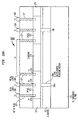
- FIG. 9a shows a plan-view of masking features used to realize several possible contacting arrangements for a surface-illuminated pixel array. More than one type of contacting arrangement is depicted on the same PD for purposes of illustration only. In practice, it is likely that only one of these arrangements would be used on a particular PD.
- a multiplicity of PD pixels tiles the photo-detecting surface (e.g., the top surface of a front-illuminated PD; the bottom surface of a back-illuminated PD).
- Four pixels 141a-141d are shown for purposes of illustration only.
- Each pixel includes doped n + -type and p + -type contacting regions 142. These doped regions are contacted by metal plugs 143, which are electrically connected to metal lines 145 overlying the ILD 148.
- the pixel stem regions are labeled 146. Because of the long diffusion transit times, it is important to limit the amount of signal light absorbed in the doped contacting regions 142.
- diffusion transit times in the doped regions are reduced by means of a light-absorbing (e.g., metal) mask that blocks signal light from reaching (and being absorbed by) part or all of the doped contacting regions.
- a light-absorbing (e.g., metal) mask that blocks signal light from reaching (and being absorbed by) part or all of the doped contacting regions.
- prior art care has not been taken to block photogeneration in these highly doped contacting regions because its impact on PD speed has not been appreciated.
- prior art devices minimize the amount of metal coverage because it reduces the QY of the PD.
- this embodiment of our invention trades a small reduction in QY for a large improvement in speed by limiting light penetration into the doped contacting regions.
- this embodiment of our invention uses metal over more than about 30% of the aggregate surface area of the doped contact regions to block a significant fraction of signal light from reaching the doped regions.
- the leftmost n + -type contacting region 142a of pixel 141a is completely occluded from light incident from above the surface, whereas the center p + -type contacting region of pixel 141a is only partly occluded.
- Another contacting scheme can be arranged to both ensure that there is no light absorption in the contacting regions while limiting the amount of pixel surface area covered by metal.
- This arrangement is shown in Fig 9a, pixel 141d.
- the doped n+ and p+ contacting regions 142a are arranged in the corners of the pixel.
- Metal covers the doped contacting regions, but since the contacting regions are in the corners instead of extending from one side of the pixel to the other (in contrast to the other pixels of Fig. 9a) they allow a larger fraction of the surface area of the pixel to absorb light.
- the doped contacting regions extend as deep into the pixel as possible in order to ensure that a high electric field exists throughout the volume of the pixel. It apparent to one skilled in the art that it is also possible to place the n+ and p+ contacting regions 142d in other regions of the pixel (as opposed to the corners) as long as high electric fields are maintained throughout the pixel and that these contacting regions are covered with metal.
- the speed of the surface-illuminated PD can be increased by directing signal light into only a portion of the middle of the pixel; e.g., the portion that lies between the doped contacting regions, as shown in pixel 141c of FIG. 9a.
- photogeneration of carriers occurs only in that portion of the pixel, and, therefore, the maximum carrier transit time to the doped contacting regions is reduced (compared to the case in which the pixel is uniformly illuminated).
- at least 30% of the top surface area of the doped contacting regions should be covered by metal.
- Pixels 141a and 141b illustrate such partial coverage of the contacting regions, whereas pixel 141c depicts complete (100%) coverage, which is preferred.
- the width of the metal not only covers the doped contacting regions, but also shadows part (e.g., at least 20%) of the top surface area of the intrinsic absorbing regions of the pixel between them.
- the upper limit for metal coverage of the pixel is not 100% but a lesser amount determined by the trade off between QY (which favors less coverage) and speed (which favors more coverage). Together this criteria define another embodiment of our invention in which metal covers at least 30% of the top surface of the doped contacting regions and more than about 20% of the top surface area of the undoped absorbing regions of the pixel between the doped contacting regions.
- this embodiment of our invention of covering the doped contacting regions by metal can improve PD speed in any type of surface-illuminated lateral PIN PD.
- Another way to limit the long diffusion transit times for the doped contacting regions, in the absence of the type of metal masking described above, is to limit the volume of the doped regions compared to the volume of the pixels, which in practice means (i) limiting the depth of the implants to around 0.2 ⁇ m in SiGe pixels, and (ii) making the width of the doped contact stripes small compared with the width of the pixel.
- the volume of the doped contacting regions within a particular pixel is less than about 25% of the volume of that pixel.
- Another technique for limiting carrier transit times is to use metal to cover the pixel stem region.
- An example of this arrangement is shown in pixel 141b of FIG. 9a.
- metal 147 completely covers the stem region 146.
- this design eliminates signal light penetration into the stem region so that no carriers are generated therein. Carriers generated in the stem region would have long transit times to the contacts.
- the volume of the stem region should be minimized compared to the volume of the pixel.
- the pixel stem region is not used for light absorption; it may contain defects that generate dark currents. Therefore, one important feature of this embodiment of our invention is that the volume of the pixel stem region be less than about 25% of the volume of the pixel.
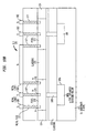
- FIG. 9b shows in plan-view several possible contacting arrangements for enhancing speed of operation. Unlike the previously described surface-illuminated PDs, it is not necessary to cover the doped contacting regions or the pixel stem regions with metal since incoming signal light is directed to the desired pixel regions (and away from the contacting regions) by means of a WG.
- FIG. 9b Two different WG-pixel combinations are shown in FIG. 9b.
- the speed of the edge-illuminated PD is increased by injecting the light into only a portion of the middle of the detector.
- the width of the WG section W 1a (W 1b ) is made less than the distance W 2a (W 2b ) between the inside edges of the doped contacting regions 157a and 158a of pixel 152a (157b and 158b of pixel 152b), and the axis of propagation of the WG is aligned to the center of the pixel portion that lies between the doped contacting regions.
- the width of the stem region (as measured transverse to the direction of light propagation) is made less than one half of the wavelength of light in the stem region material, very little light will penetrate into the stem region.
- the stem region need not be offset; it may be located anywhere in the pixel region where signal light 156b is absorbed (e.g., in the center of the pixel, as shown by stem region 151b of pixel 152b). Therefore, a further feature of this embodiment of our invention is that the width of the stem region is less than one half the wavelength of signal light in the material of the stem region.
- the width W 1a of the WG should be less than the width W 2a of the pixel, and that the propagation of the WG should be aligned to the center of the pixel.
- the propagation axis of the WG 154 is aligned between the edge of the pixel and the stem region (i.e., between the inside edge of the n + -type contacting region 157a and the stem region 151a). This feature ensures that no significant amount of light is absorbed in the stem region 151a.
- Another aspect of the current invention relates to PD contact configurations that reduce dark currents. These designs are illustrated in FIG. 10.
- the pixel stem regions are doped with either an n-type or p-type dopant to suppress dark current generation.
- This doping can be introduced in the stem regions 188a, as shown in FIG. 10a, during the pixel (e.g., SiGe) growth.
- the stem region 188a is in-situ doped n-type, and the pixel is undoped or low doped. This difference in doping is accomplished, for example, by changing the dopant gas flows during epitaxial growth.
- Another doping issue is a function of the dopant type of the substrate.
- the substrate 171 is contacted and is doped p-type (n-type)
- a large leakage current can flow from the substrate contact to either the p + -type contact regions 179 (n + -type contact regions 178) in the pixel.
- a reverse-biased PN junction be positioned between the substrate and the pixel. This junction can be accomplished in two ways. First, as shown in FIG. 10b, a PN junction blocking region 189b is formed in the substrate 171 and under the pixel 175 using ion implantation prior to deposition of the stem cladding region 188b.
- the blocking PN junction is defined by the interface 190b between the implanted region 189b and the Si substrate 171.
- the blocking PN junction is formed through in-situ doping of the pixel 175 and stem region 188a.
- the blocking junction is formed at the interface 190a between the n-type stem region 188a and the p-type substrate 171.
- This design also has the benefit of reducing possible sources of dark current. Therefore, it is also an aspect of the current invention that a PN junction is interposed between the substrate and the low doped body of the pixel.
- surface-illuminated embodiments of our invention may be front (top) -side illuminated, as previously described, or may be back (bottom) -side illuminated. In the latter case, signal light cannot be blocked from entering the doped contacting regions by metal, and so in order to avoid diffusion time limitations, the volume of the doped contacting region should be small; i.e., less than about 25% of the volume of the pixel.
- the volume of the stem regions should be kept relatively small; e.g., less than about 25% of the volume of the pixel.
Landscapes
- Engineering & Computer Science (AREA)
- Manufacturing & Machinery (AREA)
- Physics & Mathematics (AREA)
- Condensed Matter Physics & Semiconductors (AREA)
- General Physics & Mathematics (AREA)
- Computer Hardware Design (AREA)
- Microelectronics & Electronic Packaging (AREA)
- Power Engineering (AREA)
- Materials Engineering (AREA)
- Chemical & Material Sciences (AREA)
- Light Receiving Elements (AREA)
- Recrystallisation Techniques (AREA)
- Solid State Image Pick-Up Elements (AREA)
- Insulated Gate Type Field-Effect Transistor (AREA)
Priority Applications (1)
| Application Number | Priority Date | Filing Date | Title |
|---|---|---|---|
| EP06076688A EP1746638A3 (en) | 2002-12-18 | 2003-11-26 | Semiconductor devices with reduced active region defectcs and unique contacting schemes |
Applications Claiming Priority (5)
| Application Number | Priority Date | Filing Date | Title |
|---|---|---|---|
| US43435902P | 2002-12-18 | 2002-12-18 | |
| US434359P | 2002-12-18 | ||
| US10/453,037 US7012314B2 (en) | 2002-12-18 | 2003-06-03 | Semiconductor devices with reduced active region defects and unique contacting schemes |
| US453037 | 2003-06-03 | ||
| PCT/US2003/037786 WO2004061911A2 (en) | 2002-12-18 | 2003-11-26 | Semiconductor devices with reduced active region defects and unique contacting schemes |
Related Child Applications (1)
| Application Number | Title | Priority Date | Filing Date |
|---|---|---|---|
| EP06076688A Division EP1746638A3 (en) | 2002-12-18 | 2003-11-26 | Semiconductor devices with reduced active region defectcs and unique contacting schemes |
Publications (2)
| Publication Number | Publication Date |
|---|---|
| EP1573790A2 EP1573790A2 (en) | 2005-09-14 |
| EP1573790B1 true EP1573790B1 (en) | 2006-12-27 |
Family
ID=32600178
Family Applications (1)
| Application Number | Title | Priority Date | Filing Date |
|---|---|---|---|
| EP03808419A Expired - Lifetime EP1573790B1 (en) | 2002-12-18 | 2003-11-26 | Semiconductor devices with reduced active region defects and unique contacting schemes |
Country Status (8)
| Country | Link |
|---|---|
| US (2) | US7012314B2 (enExample) |
| EP (1) | EP1573790B1 (enExample) |
| JP (2) | JP5489387B2 (enExample) |
| KR (1) | KR20050093785A (enExample) |
| AU (1) | AU2003303492A1 (enExample) |
| DE (1) | DE60310762T2 (enExample) |
| TW (1) | TWI232544B (enExample) |
| WO (1) | WO2004061911A2 (enExample) |
Families Citing this family (107)
| Publication number | Priority date | Publication date | Assignee | Title |
|---|---|---|---|---|
| US6649480B2 (en) * | 2000-12-04 | 2003-11-18 | Amberwave Systems Corporation | Method of fabricating CMOS inverter and integrated circuits utilizing strained silicon surface channel MOSFETs |
| US6703688B1 (en) * | 2001-03-02 | 2004-03-09 | Amberwave Systems Corporation | Relaxed silicon germanium platform for high speed CMOS electronics and high speed analog circuits |
| US6830976B2 (en) * | 2001-03-02 | 2004-12-14 | Amberwave Systems Corproation | Relaxed silicon germanium platform for high speed CMOS electronics and high speed analog circuits |
| US6995430B2 (en) | 2002-06-07 | 2006-02-07 | Amberwave Systems Corporation | Strained-semiconductor-on-insulator device structures |
| US6946371B2 (en) * | 2002-06-10 | 2005-09-20 | Amberwave Systems Corporation | Methods of fabricating semiconductor structures having epitaxially grown source and drain elements |
| US6982474B2 (en) * | 2002-06-25 | 2006-01-03 | Amberwave Systems Corporation | Reacted conductive gate electrodes |
| US7643755B2 (en) * | 2003-10-13 | 2010-01-05 | Noble Peak Vision Corp. | Optical receiver comprising a receiver photodetector integrated with an imaging array |
| US7453129B2 (en) | 2002-12-18 | 2008-11-18 | Noble Peak Vision Corp. | Image sensor comprising isolated germanium photodetectors integrated with a silicon substrate and silicon circuitry |
| US7589380B2 (en) * | 2002-12-18 | 2009-09-15 | Noble Peak Vision Corp. | Method for forming integrated circuit utilizing dual semiconductors |
| US20060055800A1 (en) * | 2002-12-18 | 2006-03-16 | Noble Device Technologies Corp. | Adaptive solid state image sensor |
| US6960781B2 (en) | 2003-03-07 | 2005-11-01 | Amberwave Systems Corporation | Shallow trench isolation process |
| US7122392B2 (en) * | 2003-06-30 | 2006-10-17 | Intel Corporation | Methods of forming a high germanium concentration silicon germanium alloy by epitaxial lateral overgrowth and structures formed thereby |
| US7503706B2 (en) * | 2003-09-05 | 2009-03-17 | Sae Magnetics (Hong Kong) Limited | MSM photodetector assembly |
| US7579263B2 (en) | 2003-09-09 | 2009-08-25 | Stc.Unm | Threading-dislocation-free nanoheteroepitaxy of Ge on Si using self-directed touch-down of Ge through a thin SiO2 layer |
| US6919258B2 (en) * | 2003-10-02 | 2005-07-19 | Freescale Semiconductor, Inc. | Semiconductor device incorporating a defect controlled strained channel structure and method of making the same |
| EP1685701B1 (en) | 2003-10-13 | 2008-09-17 | Noble Peak Vision Corp. | Image sensor comprising isolated germanium photodetectors integrated with a silicon substrate and silicon circuitry |
| US7198970B2 (en) * | 2004-01-23 | 2007-04-03 | The United States Of America As Represented By The Secretary Of The Navy | Technique for perfecting the active regions of wide bandgap semiconductor nitride devices |
| US7186622B2 (en) * | 2004-07-15 | 2007-03-06 | Infineon Technologies Ag | Formation of active area using semiconductor growth process without STI integration |
| US20060073681A1 (en) * | 2004-09-08 | 2006-04-06 | Han Sang M | Nanoheteroepitaxy of Ge on Si as a foundation for group III-V and II-VI integration |
| US7439542B2 (en) * | 2004-10-05 | 2008-10-21 | International Business Machines Corporation | Hybrid orientation CMOS with partial insulation process |
| KR100641068B1 (ko) * | 2005-01-21 | 2006-11-06 | 삼성전자주식회사 | 듀얼 다마신 채널 구조물과 그 제조 방법 |
| US7298009B2 (en) | 2005-02-01 | 2007-11-20 | Infineon Technologies Ag | Semiconductor method and device with mixed orientation substrate |
| US8324660B2 (en) | 2005-05-17 | 2012-12-04 | Taiwan Semiconductor Manufacturing Company, Ltd. | Lattice-mismatched semiconductor structures with reduced dislocation defect densities and related methods for device fabrication |
| EP2595175B1 (en) * | 2005-05-17 | 2019-04-17 | Taiwan Semiconductor Manufacturing Company, Ltd. | Method of fabricating a lattice-mismatched semiconductor structure with reduced dislocation defect densities |
| US20070267722A1 (en) * | 2006-05-17 | 2007-11-22 | Amberwave Systems Corporation | Lattice-mismatched semiconductor structures with reduced dislocation defect densities and related methods for device fabrication |
| US9153645B2 (en) | 2005-05-17 | 2015-10-06 | Taiwan Semiconductor Manufacturing Company, Ltd. | Lattice-mismatched semiconductor structures with reduced dislocation defect densities and related methods for device fabrication |
| US7626246B2 (en) * | 2005-07-26 | 2009-12-01 | Amberwave Systems Corporation | Solutions for integrated circuit integration of alternative active area materials |
| US7459367B2 (en) | 2005-07-27 | 2008-12-02 | International Business Machines Corporation | Method of forming a vertical P-N junction device |
| US7638842B2 (en) * | 2005-09-07 | 2009-12-29 | Amberwave Systems Corporation | Lattice-mismatched semiconductor structures on insulators |
| US20070054467A1 (en) * | 2005-09-07 | 2007-03-08 | Amberwave Systems Corporation | Methods for integrating lattice-mismatched semiconductor structure on insulators |
| US7705370B2 (en) * | 2005-11-01 | 2010-04-27 | Massachusetts Institute Of Technology | Monolithically integrated photodetectors |
| US20070252223A1 (en) * | 2005-12-05 | 2007-11-01 | Massachusetts Institute Of Technology | Insulated gate devices and method of making same |
| US8530355B2 (en) * | 2005-12-23 | 2013-09-10 | Infineon Technologies Ag | Mixed orientation semiconductor device and method |
| US7629661B2 (en) * | 2006-02-10 | 2009-12-08 | Noble Peak Vision Corp. | Semiconductor devices with photoresponsive components and metal silicide light blocking structures |
| US7901968B2 (en) * | 2006-03-23 | 2011-03-08 | Asm America, Inc. | Heteroepitaxial deposition over an oxidized surface |
| US7777250B2 (en) * | 2006-03-24 | 2010-08-17 | Taiwan Semiconductor Manufacturing Company, Ltd. | Lattice-mismatched semiconductor structures and related methods for device fabrication |
| US7485524B2 (en) * | 2006-06-21 | 2009-02-03 | International Business Machines Corporation | MOSFETs comprising source/drain regions with slanted upper surfaces, and method for fabricating the same |
| US8063397B2 (en) * | 2006-06-28 | 2011-11-22 | Massachusetts Institute Of Technology | Semiconductor light-emitting structure and graded-composition substrate providing yellow-green light emission |
| EP2062290B1 (en) | 2006-09-07 | 2019-08-28 | Taiwan Semiconductor Manufacturing Company, Ltd. | Defect reduction using aspect ratio trapping |
| WO2008036256A1 (en) * | 2006-09-18 | 2008-03-27 | Amberwave Systems Corporation | Aspect ratio trapping for mixed signal applications |
| WO2008039495A1 (en) * | 2006-09-27 | 2008-04-03 | Amberwave Systems Corporation | Tri-gate field-effect transistors formed by aspect ratio trapping |
| WO2008039534A2 (en) | 2006-09-27 | 2008-04-03 | Amberwave Systems Corporation | Quantum tunneling devices and circuits with lattice- mismatched semiconductor structures |
| US8502263B2 (en) * | 2006-10-19 | 2013-08-06 | Taiwan Semiconductor Manufacturing Company, Ltd. | Light-emitter-based devices with lattice-mismatched semiconductor structures |
| US9508890B2 (en) | 2007-04-09 | 2016-11-29 | Taiwan Semiconductor Manufacturing Company, Ltd. | Photovoltaics on silicon |
| US8304805B2 (en) | 2009-01-09 | 2012-11-06 | Taiwan Semiconductor Manufacturing Company, Ltd. | Semiconductor diodes fabricated by aspect ratio trapping with coalesced films |
| US8237151B2 (en) * | 2009-01-09 | 2012-08-07 | Taiwan Semiconductor Manufacturing Company, Ltd. | Diode-based devices and methods for making the same |
| US7825328B2 (en) | 2007-04-09 | 2010-11-02 | Taiwan Semiconductor Manufacturing Company, Ltd. | Nitride-based multi-junction solar cell modules and methods for making the same |
| US8329541B2 (en) * | 2007-06-15 | 2012-12-11 | Taiwan Semiconductor Manufacturing Company, Ltd. | InP-based transistor fabrication |
| JP2010538495A (ja) | 2007-09-07 | 2010-12-09 | アンバーウェーブ・システムズ・コーポレーション | 多接合太陽電池 |
| US8871554B2 (en) * | 2007-10-30 | 2014-10-28 | Bae Systems Information And Electronic Systems Integration Inc. | Method for fabricating butt-coupled electro-absorptive modulators |
| US7723206B2 (en) * | 2007-12-05 | 2010-05-25 | Fujifilm Corporation | Photodiode |
| JP5669359B2 (ja) * | 2008-03-01 | 2015-02-12 | 住友化学株式会社 | 半導体基板、半導体基板の製造方法および電子デバイス |
| US8766318B2 (en) * | 2008-03-01 | 2014-07-01 | Sumitomo Chemical Company, Limited | Semiconductor wafer, method of manufacturing a semiconductor wafer, and electronic device |
| US8183667B2 (en) | 2008-06-03 | 2012-05-22 | Taiwan Semiconductor Manufacturing Co., Ltd. | Epitaxial growth of crystalline material |
| US8274097B2 (en) | 2008-07-01 | 2012-09-25 | Taiwan Semiconductor Manufacturing Company, Ltd. | Reduction of edge effects from aspect ratio trapping |
| US8981427B2 (en) | 2008-07-15 | 2015-03-17 | Taiwan Semiconductor Manufacturing Company, Ltd. | Polishing of small composite semiconductor materials |
| US8084739B2 (en) | 2008-07-16 | 2011-12-27 | Infrared Newco., Inc. | Imaging apparatus and methods |
| US8686365B2 (en) * | 2008-07-28 | 2014-04-01 | Infrared Newco, Inc. | Imaging apparatus and methods |
| EP2528087B1 (en) | 2008-09-19 | 2016-06-29 | Taiwan Semiconductor Manufacturing Company, Ltd. | Formation of devices by epitaxial layer overgrowth |
| US20100072515A1 (en) | 2008-09-19 | 2010-03-25 | Amberwave Systems Corporation | Fabrication and structures of crystalline material |
| US8253211B2 (en) | 2008-09-24 | 2012-08-28 | Taiwan Semiconductor Manufacturing Company, Ltd. | Semiconductor sensor structures with reduced dislocation defect densities |
| TWI471910B (zh) * | 2008-10-02 | 2015-02-01 | Sumitomo Chemical Co | 半導體晶圓、電子裝置及半導體晶圓之製造方法 |
| WO2010114956A1 (en) | 2009-04-02 | 2010-10-07 | Taiwan Semiconductor Manufacturing Company, Ltd. | Devices formed from a non-polar plane of a crystalline material and method of making the same |
| KR20120022872A (ko) * | 2009-05-22 | 2012-03-12 | 스미또모 가가꾸 가부시키가이샤 | 반도체 기판, 전자 디바이스, 반도체 기판의 제조 방법 및 전자 디바이스의 제조 방법 |
| KR101671552B1 (ko) * | 2009-06-05 | 2016-11-01 | 내셔날 인스티튜트 오브 어드밴스드 인더스트리얼 사이언스 앤드 테크놀로지 | 센서, 반도체 기판 및 반도체 기판의 제조 방법 |
| JP5414415B2 (ja) * | 2009-08-06 | 2014-02-12 | 株式会社日立製作所 | 半導体受光素子及びその製造方法 |
| SG169922A1 (en) * | 2009-09-24 | 2011-04-29 | Taiwan Semiconductor Mfg | Improved semiconductor sensor structures with reduced dislocation defect densities and related methods for the same |
| JP5969811B2 (ja) * | 2011-05-09 | 2016-08-17 | アイメックImec | シリコン・フォトニクスプラットフォーム上でのフォトニックデバイスの共集積化方法 |
| US8546250B2 (en) | 2011-08-18 | 2013-10-01 | Wafertech Llc | Method of fabricating vertical integrated semiconductor device with multiple continuous single crystal silicon layers vertically separated from one another |
| US9127345B2 (en) | 2012-03-06 | 2015-09-08 | Asm America, Inc. | Methods for depositing an epitaxial silicon germanium layer having a germanium to silicon ratio greater than 1:1 using silylgermane and a diluent |
| US9709740B2 (en) * | 2012-06-04 | 2017-07-18 | Micron Technology, Inc. | Method and structure providing optical isolation of a waveguide on a silicon-on-insulator substrate |
| US9142400B1 (en) | 2012-07-17 | 2015-09-22 | Stc.Unm | Method of making a heteroepitaxial layer on a seed area |
| US9171715B2 (en) | 2012-09-05 | 2015-10-27 | Asm Ip Holding B.V. | Atomic layer deposition of GeO2 |
| US9213137B2 (en) * | 2013-07-12 | 2015-12-15 | Globalfoundries Singapore Pte. Ltd. | Semiconductor devices including photodetectors integrated on waveguides and methods for fabricating the same |
| CN105378937B (zh) * | 2013-08-02 | 2017-08-08 | 英特尔公司 | 低电压光电检测器 |
| US10096474B2 (en) | 2013-09-04 | 2018-10-09 | Intel Corporation | Methods and structures to prevent sidewall defects during selective epitaxy |
| KR102245485B1 (ko) * | 2013-09-04 | 2021-04-29 | 인텔 코포레이션 | 선택적 에피택시 동안 측벽 결함을 방지하는 방법 및 구조 |
| US9218963B2 (en) | 2013-12-19 | 2015-12-22 | Asm Ip Holding B.V. | Cyclical deposition of germanium |
| US9799689B2 (en) | 2014-11-13 | 2017-10-24 | Artilux Inc. | Light absorption apparatus |
| US9748307B2 (en) | 2014-11-13 | 2017-08-29 | Artilux Inc. | Light absorption apparatus |
| KR102284657B1 (ko) | 2015-01-05 | 2021-08-02 | 삼성전자 주식회사 | 포토 다이오드 및 이를 포함하는 광통신 시스템 |
| KR102279162B1 (ko) * | 2015-03-03 | 2021-07-20 | 한국전자통신연구원 | 게르마늄 온 인슐레이터 기판 및 그의 형성방법 |
| CN108352393B (zh) | 2015-07-23 | 2022-09-16 | 光程研创股份有限公司 | 高效宽光谱传感器 |
| US9917189B2 (en) * | 2015-07-31 | 2018-03-13 | Taiwan Semiconductor Manufacturing Company, Ltd. | Method for detecting presence and location of defects in a substrate |
| US10707260B2 (en) | 2015-08-04 | 2020-07-07 | Artilux, Inc. | Circuit for operating a multi-gate VIS/IR photodiode |
| US10861888B2 (en) | 2015-08-04 | 2020-12-08 | Artilux, Inc. | Silicon germanium imager with photodiode in trench |
| EP3370258B1 (en) | 2015-08-04 | 2020-03-25 | Artilux Inc. | Germanium-silicon light sensing apparatus |
| US10761599B2 (en) | 2015-08-04 | 2020-09-01 | Artilux, Inc. | Eye gesture tracking |
| CN115824395B (zh) | 2015-08-27 | 2023-08-15 | 光程研创股份有限公司 | 宽频谱光学传感器 |
| US10418407B2 (en) | 2015-11-06 | 2019-09-17 | Artilux, Inc. | High-speed light sensing apparatus III |
| US10886309B2 (en) | 2015-11-06 | 2021-01-05 | Artilux, Inc. | High-speed light sensing apparatus II |
| US10741598B2 (en) | 2015-11-06 | 2020-08-11 | Atrilux, Inc. | High-speed light sensing apparatus II |
| US10254389B2 (en) | 2015-11-06 | 2019-04-09 | Artilux Corporation | High-speed light sensing apparatus |
| US10739443B2 (en) | 2015-11-06 | 2020-08-11 | Artilux, Inc. | High-speed light sensing apparatus II |
| IL242952B (en) | 2015-12-06 | 2021-02-28 | Semi Conductor Devices An Elbit Systems Rafael Partnership | Photodetector-arrays and methods of fabrication thereof |
| US20170350752A1 (en) * | 2016-06-01 | 2017-12-07 | Ventsislav Metodiev Lavchiev | Light emitting structures and systems on the basis of group iv material(s) for the ultraviolet and visible spectral ranges |
| GB2549951B (en) * | 2016-05-03 | 2019-11-20 | Metodiev Lavchiev Ventsislav | Light emitting structures and systems on the basis of group-IV material(s) for the ultra violet and visible spectral range |
| WO2018011373A1 (en) * | 2016-07-13 | 2018-01-18 | Rockley Photonics Limited | Integrated structure and manufacturing method thereof |
| CN111868929B (zh) | 2018-02-23 | 2021-08-03 | 奥特逻科公司 | 光检测装置及其光检测方法 |
| US11105928B2 (en) | 2018-02-23 | 2021-08-31 | Artilux, Inc. | Light-sensing apparatus and light-sensing method thereof |
| JP7212062B2 (ja) | 2018-04-08 | 2023-01-24 | アーティラックス・インコーポレイテッド | 光検出装置 |
| TWI795562B (zh) | 2018-05-07 | 2023-03-11 | 美商光程研創股份有限公司 | 雪崩式之光電晶體 |
| US10969877B2 (en) | 2018-05-08 | 2021-04-06 | Artilux, Inc. | Display apparatus |
| JP6836547B2 (ja) * | 2018-05-21 | 2021-03-03 | 日本電信電話株式会社 | 光検出器 |
| US10861896B2 (en) | 2018-07-27 | 2020-12-08 | Taiwan Semiconductor Manufacturing Co., Ltd. | Capping structure to reduce dark current in image sensors |
| WO2023059548A1 (en) * | 2021-10-06 | 2023-04-13 | Analog Devices Inc. | Monolithic multi-wavelength optical devcies |
| EP4167269A1 (en) * | 2021-10-15 | 2023-04-19 | Infineon Technologies AG | Heteroepitaxial semiconductor device and method for fabricating a heteroepitaxial semiconductor device |
Family Cites Families (26)
| Publication number | Priority date | Publication date | Assignee | Title |
|---|---|---|---|---|
| JPS61177742A (ja) * | 1985-02-01 | 1986-08-09 | Mitsubishi Electric Corp | 半導体装置 |
| JPS63216386A (ja) * | 1987-03-05 | 1988-09-08 | Fujitsu Ltd | 半導体受光装置 |
| JPH01184878A (ja) * | 1988-01-13 | 1989-07-24 | Mitsubishi Electric Corp | 横型pinフオトダイオードの製造方法 |
| JPH03125458A (ja) * | 1989-10-11 | 1991-05-28 | Canon Inc | 単結晶領域の形成方法及びそれを用いた結晶物品 |
| US5162891A (en) * | 1991-07-03 | 1992-11-10 | International Business Machines Corporation | Group III-V heterostructure devices having self-aligned graded contact diffusion regions and method for fabricating same |
| KR100259063B1 (ko) | 1992-06-12 | 2000-06-15 | 김영환 | Ccd 영상소자 |
| JP3930161B2 (ja) * | 1997-08-29 | 2007-06-13 | 株式会社東芝 | 窒化物系半導体素子、発光素子及びその製造方法 |
| US6057586A (en) * | 1997-09-26 | 2000-05-02 | Intel Corporation | Method and apparatus for employing a light shield to modulate pixel color responsivity |
| JP3501265B2 (ja) * | 1997-10-30 | 2004-03-02 | 富士通株式会社 | 半導体装置の製造方法 |
| WO1999044224A1 (en) | 1998-02-27 | 1999-09-02 | North Carolina State University | Methods of fabricating gallium nitride semiconductor layers by lateral overgrowth through masks, and gallium nitride semiconductor structures fabricated thereby |
| US6500257B1 (en) | 1998-04-17 | 2002-12-31 | Agilent Technologies, Inc. | Epitaxial material grown laterally within a trench and method for producing same |
| JP4032538B2 (ja) | 1998-11-26 | 2008-01-16 | ソニー株式会社 | 半導体薄膜および半導体素子の製造方法 |
| JP3824446B2 (ja) * | 1999-05-28 | 2006-09-20 | シャープ株式会社 | 固体撮像装置の製造方法 |
| US6396046B1 (en) | 1999-11-02 | 2002-05-28 | General Electric Company | Imager with reduced FET photoresponse and high integrity contact via |
| JP3455512B2 (ja) * | 1999-11-17 | 2003-10-14 | 日本碍子株式会社 | エピタキシャル成長用基板およびその製造方法 |
| TW494574B (en) | 1999-12-01 | 2002-07-11 | Innotech Corp | Solid state imaging device, method of manufacturing the same, and solid state imaging system |
| JP3827909B2 (ja) | 2000-03-21 | 2006-09-27 | シャープ株式会社 | 固体撮像装置およびその製造方法 |
| GB0014961D0 (en) * | 2000-06-20 | 2000-08-09 | Koninkl Philips Electronics Nv | Light-emitting matrix array display devices with light sensing elements |
| JP3912024B2 (ja) * | 2001-04-09 | 2007-05-09 | セイコーエプソン株式会社 | Pin構造のラテラル型半導体受光素子 |
| JP2002314116A (ja) * | 2001-04-09 | 2002-10-25 | Seiko Epson Corp | Pin構造のラテラル型半導体受光素子 |
| GB0111207D0 (en) | 2001-05-08 | 2001-06-27 | Btg Int Ltd | A method to produce germanium layers |
| JP4375517B2 (ja) * | 2001-07-23 | 2009-12-02 | 日本電気株式会社 | 液晶表示装置 |
| US7248297B2 (en) * | 2001-11-30 | 2007-07-24 | The Board Of Trustees Of The Leland Stanford Junior University | Integrated color pixel (ICP) |
| US6835954B2 (en) * | 2001-12-29 | 2004-12-28 | Lg.Philips Lcd Co., Ltd. | Active matrix organic electroluminescent display device |
| US7098069B2 (en) * | 2002-01-24 | 2006-08-29 | Semiconductor Energy Laboratory Co., Ltd. | Light emitting device, method of preparing the same and device for fabricating the same |
| TW546853B (en) * | 2002-05-01 | 2003-08-11 | Au Optronics Corp | Active type OLED and the fabrication method thereof |
-
2003
- 2003-06-03 US US10/453,037 patent/US7012314B2/en not_active Expired - Lifetime
- 2003-10-13 TW TW092128288A patent/TWI232544B/zh not_active IP Right Cessation
- 2003-11-26 JP JP2005508542A patent/JP5489387B2/ja not_active Expired - Fee Related
- 2003-11-26 AU AU2003303492A patent/AU2003303492A1/en not_active Abandoned
- 2003-11-26 WO PCT/US2003/037786 patent/WO2004061911A2/en not_active Ceased
- 2003-11-26 DE DE60310762T patent/DE60310762T2/de not_active Expired - Lifetime
- 2003-11-26 EP EP03808419A patent/EP1573790B1/en not_active Expired - Lifetime
- 2003-11-26 KR KR1020057011353A patent/KR20050093785A/ko not_active Ceased
-
2005
- 2005-11-08 US US11/269,017 patent/US7297569B2/en not_active Expired - Lifetime
-
2011
- 2011-06-22 JP JP2011138418A patent/JP2011238942A/ja active Pending
Also Published As
| Publication number | Publication date |
|---|---|
| US20040121507A1 (en) | 2004-06-24 |
| JP2011238942A (ja) | 2011-11-24 |
| DE60310762D1 (de) | 2007-02-08 |
| US7012314B2 (en) | 2006-03-14 |
| US20060057825A1 (en) | 2006-03-16 |
| AU2003303492A8 (en) | 2004-07-29 |
| WO2004061911A8 (en) | 2005-08-25 |
| AU2003303492A1 (en) | 2004-07-29 |
| US7297569B2 (en) | 2007-11-20 |
| JP2006513584A (ja) | 2006-04-20 |
| WO2004061911A3 (en) | 2004-09-16 |
| WO2004061911A2 (en) | 2004-07-22 |
| KR20050093785A (ko) | 2005-09-23 |
| JP5489387B2 (ja) | 2014-05-14 |
| TW200419721A (en) | 2004-10-01 |
| EP1573790A2 (en) | 2005-09-14 |
| TWI232544B (en) | 2005-05-11 |
| DE60310762T2 (de) | 2007-10-11 |
Similar Documents
| Publication | Publication Date | Title |
|---|---|---|
| EP1573790B1 (en) | Semiconductor devices with reduced active region defects and unique contacting schemes | |
| US20250248092A1 (en) | Superlattice materials and applications | |
| CN101002326B (zh) | 与cmos单片集成的光子器件 | |
| JP5917978B2 (ja) | 半導体装置及びその製造方法 | |
| US8872294B2 (en) | Method and apparatus for reducing signal loss in a photo detector | |
| US9748429B1 (en) | Avalanche diode having reduced dark current and method for its manufacture | |
| US7151881B2 (en) | Impurity-based waveguide detectors | |
| US20070018270A1 (en) | Embedded waveguide detectors | |
| WO2004027879A2 (en) | Light-sensing device | |
| EP0709901B1 (en) | Fabrication process for a silicon photosensitive element | |
| EP3961727A2 (en) | Diode with light-sensitive intrinsic region | |
| US7132656B2 (en) | High speed and high efficiency Si-based photodetectors using waveguides formed with silicide for near IR applications | |
| Colace et al. | Waveguide photodetectors for the near-infrared in polycrystalline germanium on silicon | |
| JP2014183194A (ja) | 半導体装置の製造方法 | |
| CN114256375B (zh) | 雪崩光电探测器及其制备方法 | |
| CN114256376B (zh) | 雪崩光电探测器及其制备方法 | |
| EP1746638A2 (en) | Semiconductor devices with reduced active region defectcs and unique contacting schemes | |
| Yamabi et al. | Fabrication of mesa-type InGaAs pin PDs with InP passivation structure on 4-inch diameter InP substrate | |
| Zimmermann | SiGe photodetectors |
Legal Events
| Date | Code | Title | Description |
|---|---|---|---|
| PUAI | Public reference made under article 153(3) epc to a published international application that has entered the european phase |
Free format text: ORIGINAL CODE: 0009012 |
|
| 17P | Request for examination filed |
Effective date: 20050617 |
|
| AK | Designated contracting states |
Kind code of ref document: A2 Designated state(s): AT BE BG CH CY CZ DE DK EE ES FI FR GB GR HU IE IT LI LU MC NL PT RO SE SI SK TR |
|
| AX | Request for extension of the european patent |
Extension state: AL LT LV MK |
|
| DAX | Request for extension of the european patent (deleted) | ||
| RBV | Designated contracting states (corrected) |
Designated state(s): DE FR GB |
|
| GRAP | Despatch of communication of intention to grant a patent |
Free format text: ORIGINAL CODE: EPIDOSNIGR1 |
|
| GRAS | Grant fee paid |
Free format text: ORIGINAL CODE: EPIDOSNIGR3 |
|
| RAP1 | Party data changed (applicant data changed or rights of an application transferred) |
Owner name: NOBLE DEVICE TECHNOLOGIES CORPORATION |
|
| GRAA | (expected) grant |
Free format text: ORIGINAL CODE: 0009210 |
|
| AK | Designated contracting states |
Kind code of ref document: B1 Designated state(s): DE FR GB |
|
| REG | Reference to a national code |
Ref country code: GB Ref legal event code: FG4D |
|
| REF | Corresponds to: |
Ref document number: 60310762 Country of ref document: DE Date of ref document: 20070208 Kind code of ref document: P |
|
| ET | Fr: translation filed | ||
| PLBE | No opposition filed within time limit |
Free format text: ORIGINAL CODE: 0009261 |
|
| STAA | Information on the status of an ep patent application or granted ep patent |
Free format text: STATUS: NO OPPOSITION FILED WITHIN TIME LIMIT |
|
| 26N | No opposition filed |
Effective date: 20070928 |
|
| REG | Reference to a national code |
Ref country code: FR Ref legal event code: CD |
|
| REG | Reference to a national code |
Ref country code: FR Ref legal event code: PLFP Year of fee payment: 13 |
|
| REG | Reference to a national code |
Ref country code: FR Ref legal event code: PLFP Year of fee payment: 14 |
|
| REG | Reference to a national code |
Ref country code: DE Ref legal event code: R082 Ref document number: 60310762 Country of ref document: DE Representative=s name: SCHMITT-NILSON SCHRAUD WAIBEL WOHLFROM PATENTA, DE |
|
| REG | Reference to a national code |
Ref country code: FR Ref legal event code: PLFP Year of fee payment: 15 |
|
| PGFP | Annual fee paid to national office [announced via postgrant information from national office to epo] |
Ref country code: DE Payment date: 20191028 Year of fee payment: 17 |
|
| PGFP | Annual fee paid to national office [announced via postgrant information from national office to epo] |
Ref country code: FR Payment date: 20191130 Year of fee payment: 17 |
|
| PGFP | Annual fee paid to national office [announced via postgrant information from national office to epo] |
Ref country code: GB Payment date: 20191125 Year of fee payment: 17 |
|
| REG | Reference to a national code |
Ref country code: DE Ref legal event code: R119 Ref document number: 60310762 Country of ref document: DE |
|
| GBPC | Gb: european patent ceased through non-payment of renewal fee |
Effective date: 20201126 |
|
| PG25 | Lapsed in a contracting state [announced via postgrant information from national office to epo] |
Ref country code: FR Free format text: LAPSE BECAUSE OF NON-PAYMENT OF DUE FEES Effective date: 20201130 |
|
| PG25 | Lapsed in a contracting state [announced via postgrant information from national office to epo] |
Ref country code: DE Free format text: LAPSE BECAUSE OF NON-PAYMENT OF DUE FEES Effective date: 20210601 Ref country code: GB Free format text: LAPSE BECAUSE OF NON-PAYMENT OF DUE FEES Effective date: 20201126 |