EP1557882A2 - Ausrichtungsverfahren, Verfahren zur Herstellung von Halbleiterbauelementen, Substrat für Halbleitervorrichtung, elektronisches Gerät - Google Patents
Ausrichtungsverfahren, Verfahren zur Herstellung von Halbleiterbauelementen, Substrat für Halbleitervorrichtung, elektronisches Gerät Download PDFInfo
- Publication number
- EP1557882A2 EP1557882A2 EP05001005A EP05001005A EP1557882A2 EP 1557882 A2 EP1557882 A2 EP 1557882A2 EP 05001005 A EP05001005 A EP 05001005A EP 05001005 A EP05001005 A EP 05001005A EP 1557882 A2 EP1557882 A2 EP 1557882A2
- Authority
- EP
- European Patent Office
- Prior art keywords
- forming
- film
- alignment mark
- substrate
- alignment
- Prior art date
- Legal status (The legal status is an assumption and is not a legal conclusion. Google has not performed a legal analysis and makes no representation as to the accuracy of the status listed.)
- Withdrawn
Links
Images





Classifications
-
- G—PHYSICS
- G03—PHOTOGRAPHY; CINEMATOGRAPHY; ANALOGOUS TECHNIQUES USING WAVES OTHER THAN OPTICAL WAVES; ELECTROGRAPHY; HOLOGRAPHY
- G03F—PHOTOMECHANICAL PRODUCTION OF TEXTURED OR PATTERNED SURFACES, e.g. FOR PRINTING, FOR PROCESSING OF SEMICONDUCTOR DEVICES; MATERIALS THEREFOR; ORIGINALS THEREFOR; APPARATUS SPECIALLY ADAPTED THEREFOR
- G03F7/00—Photomechanical, e.g. photolithographic, production of textured or patterned surfaces, e.g. printing surfaces; Materials therefor, e.g. comprising photoresists; Apparatus specially adapted therefor
- G03F7/20—Exposure; Apparatus therefor
- G03F7/2022—Multi-step exposure, e.g. hybrid; backside exposure; blanket exposure, e.g. for image reversal; edge exposure, e.g. for edge bead removal; corrective exposure
- G03F7/2026—Multi-step exposure, e.g. hybrid; backside exposure; blanket exposure, e.g. for image reversal; edge exposure, e.g. for edge bead removal; corrective exposure for the removal of unwanted material, e.g. image or background correction
- G03F7/2028—Multi-step exposure, e.g. hybrid; backside exposure; blanket exposure, e.g. for image reversal; edge exposure, e.g. for edge bead removal; corrective exposure for the removal of unwanted material, e.g. image or background correction of an edge bead on wafers
-
- H—ELECTRICITY
- H10—SEMICONDUCTOR DEVICES; ELECTRIC SOLID-STATE DEVICES NOT OTHERWISE PROVIDED FOR
- H10D—INORGANIC ELECTRIC SEMICONDUCTOR DEVICES
- H10D30/00—Field-effect transistors [FET]
- H10D30/01—Manufacture or treatment
- H10D30/021—Manufacture or treatment of FETs having insulated gates [IGFET]
- H10D30/031—Manufacture or treatment of FETs having insulated gates [IGFET] of thin-film transistors [TFT]
- H10D30/0312—Manufacture or treatment of FETs having insulated gates [IGFET] of thin-film transistors [TFT] characterised by the gate electrodes
- H10D30/0314—Manufacture or treatment of FETs having insulated gates [IGFET] of thin-film transistors [TFT] characterised by the gate electrodes of lateral top-gate TFTs comprising only a single gate
-
- H—ELECTRICITY
- H10—SEMICONDUCTOR DEVICES; ELECTRIC SOLID-STATE DEVICES NOT OTHERWISE PROVIDED FOR
- H10D—INORGANIC ELECTRIC SEMICONDUCTOR DEVICES
- H10D30/00—Field-effect transistors [FET]
- H10D30/01—Manufacture or treatment
- H10D30/021—Manufacture or treatment of FETs having insulated gates [IGFET]
- H10D30/031—Manufacture or treatment of FETs having insulated gates [IGFET] of thin-film transistors [TFT]
- H10D30/0321—Manufacture or treatment of FETs having insulated gates [IGFET] of thin-film transistors [TFT] comprising silicon, e.g. amorphous silicon or polysilicon
-
- H—ELECTRICITY
- H10—SEMICONDUCTOR DEVICES; ELECTRIC SOLID-STATE DEVICES NOT OTHERWISE PROVIDED FOR
- H10D—INORGANIC ELECTRIC SEMICONDUCTOR DEVICES
- H10D86/00—Integrated devices formed in or on insulating or conducting substrates, e.g. formed in silicon-on-insulator [SOI] substrates or on stainless steel or glass substrates
- H10D86/40—Integrated devices formed in or on insulating or conducting substrates, e.g. formed in silicon-on-insulator [SOI] substrates or on stainless steel or glass substrates characterised by multiple TFTs
-
- H—ELECTRICITY
- H10—SEMICONDUCTOR DEVICES; ELECTRIC SOLID-STATE DEVICES NOT OTHERWISE PROVIDED FOR
- H10W—GENERIC PACKAGES, INTERCONNECTIONS, CONNECTORS OR OTHER CONSTRUCTIONAL DETAILS OF DEVICES COVERED BY CLASS H10
- H10W46/00—Marks applied to devices, e.g. for alignment or identification
-
- H—ELECTRICITY
- H10—SEMICONDUCTOR DEVICES; ELECTRIC SOLID-STATE DEVICES NOT OTHERWISE PROVIDED FOR
- H10D—INORGANIC ELECTRIC SEMICONDUCTOR DEVICES
- H10D86/00—Integrated devices formed in or on insulating or conducting substrates, e.g. formed in silicon-on-insulator [SOI] substrates or on stainless steel or glass substrates
- H10D86/01—Manufacture or treatment
- H10D86/021—Manufacture or treatment of multiple TFTs
- H10D86/0241—Manufacture or treatment of multiple TFTs using liquid deposition, e.g. printing
-
- H—ELECTRICITY
- H10—SEMICONDUCTOR DEVICES; ELECTRIC SOLID-STATE DEVICES NOT OTHERWISE PROVIDED FOR
- H10W—GENERIC PACKAGES, INTERCONNECTIONS, CONNECTORS OR OTHER CONSTRUCTIONAL DETAILS OF DEVICES COVERED BY CLASS H10
- H10W46/00—Marks applied to devices, e.g. for alignment or identification
- H10W46/501—Marks applied to devices, e.g. for alignment or identification for use before dicing
Definitions
- the present invention relates to an alignment method, a method for manufacturing a semiconductor device, a substrate for a semiconductor device, and electronic equipment.
- the liquid-phase processing provides the following advantages over the conventional vacuum processing that involves evaporation.
- Patent Document 1 discloses some prior art relating to the background of the invention.
- liquid-phase processing provides high-performance devices by planarizing the surface of their films. While manufacturing such devices, however, the planarization of surface of their films may cause a problem. Specifically, when forming a thin film by liquid-phase processing (e.g. spin coating), a concave-convex pattern positioned under the thin film is planarized by the thin film. Therefore, if a film that does not transmits light is formed on the thin film for patterning, it is difficult to make an alignment based on the pattern on the surface of the film like in conventional photo processing.
- liquid-phase processing e.g. spin coating
- the gate insulating film or interlayer insulating film of a thin-film transistor is formed by liquid-phase processing, the surface of a metal film formed on the insulating film has no concave-convex pattern, and thereby it cannot be correctly aligned with an underlying semiconductor film.
- the present invention aims to provide an alignment method that is preferably applicable when manufacturing equipments by liquid-phase processing.
- an alignment method of the present invention includes the following steps in a device manufacturing process including forming of a functional film on a substrate by liquid-phase processing:
- Using the alignment mark can provide accurate patterning of a film that is formed after forming the functional film.
- a "functional film” is a collective term referring to films with predetermined functions.
- functions may include electric and electronic functions (e.g. conductive, insulating, piezoelectric, pyroelectric, and dielectric properties), optical functions (e.g. photoselective absorption, reflectivity, polarization, photoselective transmission, nonlinear optical properties, luminescence such as fluorescence and phosphorescence, photochromic properties), magnetic functions (e.g. hard magnetism, soft magnetism, nonmagnetism, permeability), chemical functions (e.g. absorption, desorption, catalysis, water absorption, ion conductivity, oxidation-reduction properties, electrochemical characteristics, electrochromic properties), mechanical functions (e.g. abrasion resistance), thermal functions (e.g. thermal conductivity, thermal insulation, infrared radiation), and biological functions (e.g. biocompatibility, antithrombogenicity).
- electric and electronic functions e.g. conductive, insulating, piezoelectric,
- Liquid-phase processing refers to methods for depositing a liquid material on a substrate. Examples of such methods may include spin coating, slit coating, dip coating, spray coating, printing, and droplet delivery methods.
- the step of forming an alignment mark may include the step of forming an alignment mark that is high enough to remain above the level of planarization by the functional film between the substrate and the functional film.
- This method is to form a high alignment mark that is high enough to remain above the level of planarization by the functional film on the substrate before forming the functional film. More specifically, this may be achieved by the following methods.
- the step of forming a second alignment mark may include the step of selectively dropping a liquid material containing the alignment mark forming material in a region for forming the first alignment mark by a droplet delivery method.
- the step of forming an alignment mark may include the step of forming the functional film that is transmissive on the substrate having a first alignment mark, and then forming a second alignment mark on the functional film by using the first alignment mark that is visible through the transmissive functional film.
- This method is to use an alignment mark provided on the substrate in advance (first alignment mark) for making another alignment mark (second alignment mark) after forming the functional film.
- the relative position of the second alignment mark may be determined by the position of the first alignment mark. This way, non-alignment between a film formed before forming the functional film and a film formed after forming the functional film can be prevented.
- the second alignment mark is not necessarily placed at the same position as that of the first alignment mark. However, if the first alignment mark and the second alignment mark are placed in almost the same position on a plane surface, a film formed after forming the functional film can be aligned more accurately.
- Another alignment method of the present invention includes the following step in a device manufacturing process including forming of a functional film on a substrate having an alignment mark by liquid-phase processing:
- the functional film is not provided in a region for forming the alignment mark. Therefore, the concave-convex pattern of the alignment mark is not planarized by the functional film. As a result, this method also can provide accurate patterning of a film that is formed after forming the functional film.
- the functional film may be formed by the following methods.
- the functional film may be patterned by the following methods.
- the position of the alignment mark is detected, and then only the functional film that is placed in this position is removed accurately.
- the method (b) when the position of the alignment mark is known to a certain extent, the functional film that is placed in and near a position in which the alignment mark is considered to be provided is roughly removed.
- the method (b) does not necessarily require a transmissive film as the functional film, and an opaque material can also be used.
- a method for manufacturing a semiconductor device according to the present invention includes any of the above-mentioned alignment methods in order to manufacture a semiconductor device. This method can provide high performance semiconductor devices.
- the method for manufacturing a semiconductor device includes the step of forming of an insulating film on a substrate by liquid-phase processing, and includes the following steps:
- Using the alignment mark can provide accurate patterning of a film that is formed after forming the insulating film.
- alignment refers to the state in which positional relationship between objects is under control. Forming the alignment mark in alignment with the second semiconductor film means that the two are formed under a certain condition, for example, the two are overlapped or spaced at a predetermined ratio, or in contact with each other.
- an “active layer” refers to layers that make up a semiconductor device and electrically function, such as a channel part of a transistor. Patterned layers used only as alignment marks are not included in this.
- Liquid-phase processing is a collective term referring to methods for providing a thin film with a liquid material on a substrate. Examples of such methods may include spin coating, slit coating, dip coating, spray coating, printing, and droplet delivery methods.
- the step of forming an alignment mark may include the step of forming an alignment mark that is high enough to remain above the level of planarization by the insulating film between the substrate and the insulating film. This method is to form a high alignment mark that is high enough to remain above the level of planarization by the insulating film on the substrate before forming the insulating film. More specifically, the step of forming an alignment mark may include the step of forming an alignment mark that is high enough to remain above the level of planarization by the insulating film at the predetermined position. In this case, the step of forming an alignment mark may include the step of forming an alignment mark that is high enough to remain above the level of planarization by the insulating film at the predetermined position.
- Another method for manufacturing a semiconductor device includes the step of forming of an insulating film on a substrate by liquid-phase processing, and includes the following steps:
- This method is to provide the surface of a film that is formed after forming the insulating film with a concave-convex pattern reflecting a concave-convex pattern (an opening, for example) created on the insulating film, and pattern the film that is formed after forming the insulating film by using the concave-convex pattern, as an alignment mark, provided on the film.
- this method also can provide accurate patterning of a film that is formed after forming the insulating film.
- the insulating-film non-forming region may be provided in a planar area of the second semiconductor film.
- the pattern of the second semiconductor film appears on the surface of a film that is formed after forming the insulating film, and thereby providing higher alignment accuracy than in a case in which the non-forming region is provided in a different position.
- the step of forming the insulating film may include the steps of forming a mask member at the predetermined position, forming the insulating film on a whole surface of the substrate except for the mask member, and removing the mask member.
- This method is to provide the insulating film with a non-forming region (opening) at the predetermined position by removing the mask member, provided on the substrate before forming the insulating film, after forming the insulating film.
- This method causes less damage on the substrate than in a case in which the opening is formed on the insulating film by etching. Even if the insulating film is made of an opaque material, the opening can be formed accurately at the predetermined position.
- the mask member may be formed by the following methods.
- Another method for manufacturing a semiconductor device according to the present invention includes the step of forming of a functional film on a substrate by liquid-phase processing, and includes the following steps:
- This method is to make a functional-film non-forming region (opening) by using the mask member formed on the substrate in advance, and pattern the functional film with high accuracy of alignment with an underlying layer (the semiconductor film, for example) by using the non-forming region as an alignment mark.
- This method can surely align the functional film with an underlying layer with high accuracy, even if the functional film is made of an opaque film.
- a substrate according to the present invention is a substrate on which a plurality of wiring layers are stacked with a functional film therebetween.
- the functional film is formed by liquid-phase processing.
- the substrate is provided with an alignment mark in a way that the pattern of the alignment mark appears on a film that is formed after forming the functional film on the substrate. Using the alignment mark can provide patterning of a wiring layer that is formed after forming the functional film with high accuracy of alignment with a wiring layer that is formed before forming the functional film.
- Electronic equipment of the present invention includes a semiconductor device manufactured by any of the above-mentioned methods for manufacturing a semiconductor device. This method can provide high performance electronic equipment.
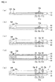
- FIGs. 1 and 2 are process drawings illustrating a method for manufacturing a thin-film transistor (TFT) which is an example of semiconductor devices according to the present embodiment.
- TFT thin-film transistor
- the drawings schematically show a transistor forming region and an alignment mark forming region in a magnified form.
- a substrate 10 having an alignment mark 10a as shown in FIG. 1A is provided as a substrate for manufacturing a semiconductor device (substrate for a semiconductor device).
- the substrate 10 may include both insulating substrates made of quartz, glass, heat-resistant plastic, etc., and conductive substrates made of semiconductor materials (e.g. silicon wafers), stainless materials, etc.
- an underlying protective film made of an insulating material such as a silicon oxide film, silicon nitride film, or silicon oxide nitride film, can be formed if necessary, so that sodium and other moving ions contained in the substrate do not get mixed in a semiconductor film that will be described later.
- a semiconductor film 11 is deposited on the substrate 10. While the semiconductor film 11 is an amorphous silicon film in this example, the semiconductor film 11 may be made of other semiconductor materials such as germanium. Otherwise, semiconductor films of a complex of Group IV elements, e.g. silicon and germanium, silicon and carbide, germanium and carbide; semiconductor films of a complex compound of Group III and Group V elements, e.g. gallium and arsenic, indium and antimony; and semiconductor films of a complex compound of Group II and Group VI elements, e.g. cadmium and selenium can be used.
- Group IV elements e.g. silicon and germanium, silicon and carbide, germanium and carbide
- semiconductor films of a complex compound of Group III and Group V elements e.g. gallium and arsenic, indium and antimony
- semiconductor films of a complex compound of Group II and Group VI elements e.g. cadmium and selenium
- semiconductor films of a further complex compound such as silicon, germanium, gallium, and arsenic; N-type semiconductor films that are such semiconductor films in which donor elements of, for example, phosphorous (P), arsenic (As), or antimony (Sb) are doped; and P-type semiconductor films that are such semiconductor films in which acceptor elements of, for example, boron, aluminum (Al), gallium (Ga), or indium (In), are doped can also be used.
- the semiconductor film 11 is formed by chemical vapor deposition (CVD) such as atmospheric pressure CVD (APCVD), low pressure CVD (LPCVD), and plasma enhanced CVD (PECVD), and physical vapor deposition (PVD) such as sputtering and evaporation.
- CVD chemical vapor deposition
- APCVD atmospheric pressure CVD
- LPCVD low pressure CVD
- PECVD plasma enhanced CVD
- PVD physical vapor deposition
- crystallization means providing an amorphous semiconductor film with thermal energy so as to transform it into a polycrystalline or single crystal silicon film, and also means providing a microcrystalline or polycrystalline semiconductor film with thermal energy so as to recrystallize it by improving the quality of the crystalline film or by melting and solidifying it.
- crystallization refers not only to the crystallization of amorphous substances but also to the crystallization of polycrystalline and microcrystalline substances.
- Examples of crystallization processing of the semiconductor film 11 may include, but not be limited to, laser irradiation, rapid heating (e.g. lamp annealing, thermal annealing), and solid-phase growth.
- Laser annealing is employed in this example to crystallize the semiconductor film 11, which is amorphous, so as to transform it into a polycrystalline semiconductor film.
- an excimer laser, argon ion laser, the second and third harmonic of an yttrium-aluminum-garnet (YAG) laser, etc. with a wavelength within or around the range of UV rays are preferably used as laser light.
- a line beam of an excimer laser whose longer length is 400 mm with an output strength of 400 mJ/cm 2 can be used. It is desirable to scan a line beam with the parts corresponding to 90% of the peak value of its laser strength in its shorter length direction overlapped in each region.
- This isolation process forms a polycrystalline semiconductor film 11a having a predetermined shape as shown in FIG. 1C on the substrate 10.
- an alignment mark material 10b is deposited onto the existing alignment mark (first alignment mark) 10a, so as to form a thick-film alignment mark (second alignment mark) AM1.
- Resist or other insulating materials can be used here as the alignment mark material 10b.
- the film of a transmissive resist is formed on the whole surface of the substrate by spin coating, for example, and then the resist is patterned by using the alignment mark 10a, which is visible through this transmissive resist.
- the insulating material is dispersed in a solvent or dispersing medium such as xylene, and the solution (i.e.
- a liquid material containing an alignment mark material is selectively dropped onto a region for forming the alignment mark 10a by a droplet delivery method (e.g. ink jetting). Then the drops are dried or burned.
- a droplet delivery method e.g. ink jetting
- other known patterning methods e.g. etching
- the alignment mark 10a By making the alignment mark 10a into the thick-film alignment mark AM1 in this step, it is possible to prevent the alignment mark AM1 from getting buried in a gate insulating film (functional film) when forming the gate insulating film by liquid-phase processing on the mark. Therefore, the pattern of the mark will appear on the films formed after forming the gate insulating film.
- the gate insulating film is formed by applying a liquid material, the concave-convex pattern of a low alignment mark is planarized by the fluidity of the liquid material. If an opaque film of Ta, Cr, or the like that is a wiring material is formed on the gate insulating film in this state, the position and shape of the alignment mark lying underneath cannot be detected. Meanwhile, the method of this example makes an alignment pattern thick enough not to get buried in the gate insulating film, and thereby accurately patterning a wiring material in a subsequent step.
- the height of the alignment mark AM1 is set high enough to remain above the level of the planarization by the gate insulating film for the above reason, and is sufficiently about 1 ⁇ m, for example.
- FIG. 1D shows an example in which the alignment mark material 10b is placed directly upon the alignment mark 10a, it is also possible to deposit the alignment mark material 10b in a wider area than the alignment mark 10a so as to completely cover the alignment mark 10a according to the present embodiment.
- a gate insulating film (functional film) 12 of TFT is deposited on the whole surface of the substrate by liquid-phase processing so as to cover the semiconductor film 11a.
- an embrocation containing xylene mixed with polysilazane (a liquid material containing polysilazane) is spin-coated on the substrate.
- prebaking is performed at 100 degrees Celsius for five minutes.
- heat treatment is performed at 350 degrees Celsius in a wet O 2 atmosphere for 260 minutes. Performing the heat treatment in a wet O 2 atmosphere can reduce nitrogen components in the insulating film that cause polarization.
- the gate insulating film 12 made of silicon oxide is provided. Since the alignment mark AM1 gets thickened in the preceding step in this example, a concave-convex part 12A reflecting the concave-convex pattern of the alignment mark AM1, which is underlying, is created on the surface of the gate insulating film 12.
- a washing step can be added if necessary between the steps of forming a semiconductor film and forming a gate insulating film. More specifically, after finishing patterning the semiconductor film 11a, the substrate is irradiated with ultraviolet (UV) rays in an oxygen-containing atmosphere so as to resolve and remove contaminants (organic matters etc.) remaining on the surface of the substrate.
- UV rays used here are provided by a low-pressure mercury lamp with its peak strength at a wavelength of 254 nm, or an excimer lamp with its peak strength at a wavelength of 172 nm.
- the light of a wavelength within this range converts oxygen molecules (O 2 ) into ozone (O 3 ) , and further into oxygen radicals (O*) . Therefore, by using ozone or oxygen radicals produced here and having high degrees of activity, it is possible to efficiently remove organic matters attached to the surface of the substrate.
- a gate wiring film 13 is deposited on the gate insulating film 12.
- the gate wiring film 13 is formed by depositing or stacking layers of adequate metal (e.g. tantalum, aluminum, titanium), metal nitride, polysilicon, or other materials by an adequate deposition method, such as sputtering, CVD, and evaporation.
- the gate wiring film 13 that is opaque is provided on the whole surface of the substrate in this step. Since the gate insulating film 12 has the concave-convex part 12A reflecting the thick-film alignment mark AM1 as mentioned above, a concave-convex part 13A reflecting this concave-convex pattern is created on the surface of the gate wiring film 13 as well.
- the gate wiring film 13 is patterned so as to form a gate wiring (wiring layer) 13a including a gate electrode. Since the surface of the gate wiring film 13 has a concave-convex pattern reflecting the pattern of the alignment mark AM1, which is underlying, in this example as mentioned above, it is possible to pattern the gate wiring film 13 with high accuracy of alignment with the semiconductor film 11a, which is underlying.
- impurity ions are doped in the semiconductor film 11a by using the gate wiring 13a as a mask, and thereby forming a source region 11s and a drain region 11d.
- the gate wiring 13a serves as a mask for doping ions
- a channel region 11c has a self-alignment structure that is provided only in a portion under the gate electrode.
- ion doping and ion implantation can be used for this impurity ion doping.
- a hydride of an element to be doped as an impurity and hydrogen are doped by using a mass non-separation ion doping device.
- raw material gases used in the ion doping process may include a hydride of an element to be doped as an impurity, such as phosphine (PH 3 ) or diborane (B 2 H 6 ) , that is diluted in hydrogen.
- a hydride of an element to be doped as an impurity such as phosphine (PH 3 ) or diborane (B 2 H 6 ) , that is diluted in hydrogen.
- the impurity is activated.
- An adequate method can be used for this activation, for example, laser irradiation, heating in a furnace at a 300 degrees Celsius or higher (low-temperature heat treatment), and rapid thermal processing using a lamp.
- another alignment mark AM2 is formed on the gate insulating film 12.
- the alignment mark AM2 is to be used for patterning a source wiring and a drain wiring that will be described later. More specifically, since an interlayer insulating film (functional film) provided between the source and drain wirings and the gate insulating film 12 is formed by liquid-phase processing in this example as will be described in greater detail, the alignment mark AM2 is made thick enough to prevent the concave-convex pattern of the alignment mark AM1 appearing on the surface of the gate insulating film 12 from being planarized by the interlayer insulating film. The height of the alignment mark AM2 is set high enough to remain above the level of planarization by the interlayer insulating film for this reason.
- Resist or other insulating materials can be used to make the alignment mark AM2, like the alignment mark material 10b.
- the film of a transmissive resist is deposited on the whole surface of the substrate by spin coating, for example, and then the resist is patterned by using the alignment mark AM1, which is visible through this transmissive resist.
- the insulating material is dispersed in a solvent or dispersing medium such as xylene, and the solution (i.e. a liquid material containing an alignment mark material) is selectively dropped onto a region for forming the alignment mark AM1 by a droplet delivery method. Then the drops are dried or burned.
- a droplet delivery head is aligned by using the alignment mark AM1, which is visible through the gate insulating film 12.
- other known patterning methods e.g. etching
- the position of forming the alignment mark AM2 is not necessarily the same as that of the alignment mark AM1. If a sufficient alignment accuracy is assured between lower wiring layers (e.g. the gate wiring 13a) and higher wiring layers (e.g. source and drain wirings), the alignment mark AM2 can be formed in a different position. For example, if the relative position of the alignment mark AM2 is controlled based on the position of the alignment mark AM1, which is in a lower layer, it is at least possible to align upper wiring layers with lower wiring layers with a certain accuracy level.
- the alignment mark AM2 which is the second alignment mark
- the alignment mark AM1 and the alignment mark AM2 placed in almost the same position on a plane surface can provide a higher alignment accuracy between the upper and lower wiring layers.
- an interlayer insulating film (functional film) 14 is deposited on the whole surface of the substrate so as to cover the gate insulating film 12 and the gate wiring 13a.
- the forming method of the interlayer insulating film 14 is the same as that of the gate insulating film 12. Specifically, an embrocation containing xylene mixed with polysilazane (a liquid material containing polysilazane) is spin-coated on the substrate. Then, prebaking is performed at 100 degrees Celsius for five minutes. Subsequently, heat treatment is performed at 350 degrees Celsius in a wet O 2 atmosphere for 260 minutes.
- a contact hole H1 is formed in a position corresponding to a source region of the interlayer insulating film 14 and the gate insulating film 12.
- a contact hole H2 is formed in a position corresponding to a drain region of the interlayer insulating film 14 and the gate insulating film 12.
- a metal film 15 of aluminum, chromium, tantalum, or the like is deposited by sputtering, PVD, or other methods so as to cover the inner wall of the contact holes H1 and H2.
- the metal film 15 that is opaque is provided on the whole surface of the substrate. Since the interlayer insulating film 14 has the concave-convex part 14A reflecting the thick-film alignment mark AM2 as mentioned above, a concave-convex part 15A reflecting this concave-convex pattern is created on the surface of the metal film 15 as well.
- the metal film 15 is patterned so as to form a source wiring (wiring layer) 15a including a source electrode and a drain wiring (wiring layer) 15b including a drain electrode.
- the surface of the metal film 15 has a concave-convex pattern reflecting the pattern of the alignment mark AM2, which is underlying, in this example as mentioned above. Therefore, it is possible to pattern the metal film 15 with high accuracy of alignment with the semiconductor film 11a and the gate wiring 13a, which are underlying.
- a protective film can be provided by depositing silicon oxide, silicon nitride, phosphosilicate glass (PSG), or the like if necessary.
- a thin-film transistor (semiconductor device) 1 is thus manufactured through the above-mentioned steps.
- the method for manufacturing a semiconductor device of the present embodiment includes liquid-phase processing in part of its manufacturing steps, which provides highly flat film surfaces. Therefore, no breaking or other problems occur in forming wirings because of a step between them, which makes it possible to manufacture highly reliable transistors with a high yield ratio.
- an alignment mark is thickened and made into a thick-film alignment mark, so that the pattern of the alignment mark will not get buried in the functional films.
- the pattern of the alignment mark appears on films formed after forming the functional films. Therefore, the films formed after forming the functional films can be patterned with high accuracy of alignment with an underlying semiconductor film, wiring layer, etc.
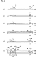
- FIGs. 3 and 4 are process drawings illustrating a method for manufacturing a TFT which is an example of semiconductor devices according to the present embodiment.
- the drawings schematically show a transistor forming region and an alignment mark forming region in a magnified form.
- the same members and elements as those in the first embodiment will be given the same reference numerals, and further description thereof will be omitted.
- the substrate 10 having the alignment mark (first alignment mark) 10a as shown in FIG. 3A is provided as a substrate for manufacturing a semiconductor device (substrate for a semiconductor device).
- a semiconductor film made of amorphous silicon or the like is deposited as shown in FIG. 3B.
- the semiconductor film is crystallized by laser annealing, for example, and isolated by etching, for example.
- the polycrystalline semiconductor film 11a having a predetermined shape as shown in FIG. 3C is formed on the substrate 10. This process is the same as that of the first embodiment.
- the gate insulating film (functional film) 12 of TFT is deposited on the semiconductor film 11a by liquid-phase processing.
- the gate insulating film 12 is provided in a region other than the region for forming the alignment mark 10a.
- the following methods can be used.
- the method of forming a self-assembled film composed of an organic molecular film or the like on the substrate surface for example, the method of forming a self-assembled film composed of an organic molecular film or the like on the substrate surface, or the method including plasma treatment can be used.
- a self-assembled film composed of an organic molecular film or the like is formed on the substrate surface on which the gate insulating film 12 is to be formed.
- the organic molecular film has a first functional group that can bond with the substrate, a second functional group that modifies the properties of the substrate surface (controlling surface energy) such as a lyophilic or lyophobic group on the opposite side of the first functional group, and a normal or partially branched carbon chain that interconnects these functional groups.
- fluoroalkylsilane such as: heptadecafluoro-1,1,2,2-tetrahydrodecyltriethoxysilane; heptadecafluoro-1,1,2,2-tetrahydrodecyltrimethoxysilane; heptadecafluoro-1,1,2,2-tetrahydrodecyltrichlorosilane; tridecafluoro-1,1,2,2-tetrahydrooctyltriethoxysilane; tridecafluoro-1,1,2,2-tetrahydrooctyltrimethoxysilane; tridecafluoro-1,1,2,2-tetrahydrooctyltrichlorosilane; and trifluoropropyltrimethoxysilane can be used here.
- FAS fluoroalkylsilane
- One of these compounds may be used alone, or alternatively two or more of them may be used in combination.
- Using FAS can provide high adhesiveness to the substrate and good liquid repellency.
- This organic molecular film can be easily patterned by being irradiated with ultraviolet rays or the like.
- the substrate is irradiated with plasma at normal pressure or in a vacuum.
- a kind of gas for the plasma treatment is selected considering, for example, the surface material of the substrate on which a conductive wiring is to be formed.
- the treatment gas used here could be tetrafluoromethane, perfluorohexane, or perfluorodecane or the like.
- a gate insulating film Provided on the surface of the substrate that has been treated as mentioned above is a gate insulating film. Specifically, an embrocation containing xylene mixed with polysilazane (a liquid material containing polysilazane) is spin-coated on the substrate. Then, prebaking is performed at 100 degrees Celsius for five minutes. Subsequently, heat treatment is performed at 350 degrees Celsius in a wet O 2 atmosphere for 260 minutes.
- the gate insulating film 12 composed of a polysilazane burned film is formed in the same manner as described in the first embodiment, and then part of the film is selectively removed by etching, for example.
- the gate insulating film can be removed by the following methods.
- the position of the alignment mark 10a is detected, and then only the gate insulating film 12 that is placed in this position is removed accurately.
- the gate insulating film 12 that is placed in and near a position in which the alignment mark 10a is considered to be provided is roughly removed.
- the method (b) does not necessarily require a transmissive film as the gate insulating film 12, and an opaque material can also be used.
- the gate wiring film 13 is deposited on the whole surface of the substrate.
- the gate wiring film 13 is formed by depositing or stacking layers of adequate metal (e.g. tantalum, aluminum, titanium), metal nitride, polysilicon, or other materials by an adequate deposition method, such as sputtering, CVD, and evaporation.
- the gate wiring film 13 that is opaque is provided on the whole surface of the substrate in this step. Since the gate insulating film 12 has the opening12B so as to expose the alignment mark 10a as mentioned above, a concave-convex part 13B reflecting the concave-convex pattern of the alignment mark 10a is created on the surface of the gate wiring film 13 as well.
- the gate wiring film 13 is patterned so as to form the gate wiring (wiring layer) 13a including a gate electrode. Since the surface of the gate wiring film 13 has a concave-convex pattern reflecting the pattern of the alignment mark 10a, which is underlying, in this example as mentioned above, it is possible to pattern the gate wiring film 13 with high accuracy of alignment with the semiconductor film 11a, which is underlying.
- impurity ions are doped in the semiconductor film 11a by using the gate wiring 13a as a mask, and thereby forming the source region 11s and the drain region 11d. Since the gate wiring 13a serves as a mask for doping ions, the channel region 11c has a self-alignment structure that is provided only in a portion under the gate electrode.
- the impurity is activated.
- An adequate method can be used for this activation, for example, laser irradiation, heating in a furnace at a 300 degrees Celsius or higher (low-temperature heat treatment), and rapid thermal processing using a lamp.
- an interlayer insulating film (functional film) 14 is deposited by liquid-phase processing so as to cover the gate insulating film 12 and the gate wiring 13a.
- the interlayer insulating film 14 is provided in a region other than the region for forming the alignment mark 10a.
- the methods similar to those described in the preceding step for forming the gate insulating film can be used. This way the interlayer insulating film 14 having an opening 14B communicating with the opening 12B of the gate insulating film 12 is provided on the gate insulating film 12.
- the contact hole H1 is formed in a position corresponding to a source region of the interlayer insulating film 14 and the gate insulating film 12.
- the contact hole H2 is formed in a position corresponding to a drain region of the interlayer insulating film 14 and the gate insulating film 12.
- a metal film 15 of aluminum, chromium, tantalum, or the like is deposited by sputtering, PVD, or other methods so as to cover the inner wall of the contact holes H1 and H2 and the openings 14B and 12B.
- the metal film 15 that is opaque is provided on the whole surface of the substrate in this step. Since the interlayer insulating film 14 has the opening 14B so as to expose the alignment mark 10a as mentioned above, a concave-convex part 15B reflecting the concave-convex pattern of the alignment mark 10a is created on the surface of the metal film 15 as well.
- the metal film 15 is patterned so as to form the source wiring (wiring layer) 15a including a source electrode and the drain wiring (wiring layer) 15b including a drain electrode.
- the surface of the metal film 15 has a concave-convex pattern reflecting the pattern of the alignment mark 10a, which is underlying, in this example as mentioned above. Therefore, it is possible to pattern the metal film 15 with high accuracy of alignment with the semiconductor film 11a and the gate wiring 13a, which are underlying.
- a protective film can be provided by depositing silicon oxide, silicon nitride, PSG, or the like if necessary.
- a thin-film transistor (semiconductor device) 2 is thus manufactured through the above-mentioned steps.
- the pattern of the alignment mark appears on films formed after forming the functional films by liquid-phase processing. Therefore, the films formed after forming the functional films can be patterned with high accuracy of alignment with an underlying semiconductor film, wiring layer, etc.
- FIGs. 5 and 6 are process drawings illustrating a method for manufacturing a TFT which is an example of semiconductor devices according to the present embodiment.
- the drawings are sectional views schematically showing a TFT forming region (element area) E1 and an alignment mark forming region (alignment area) E2 in a magnified form.
- a substrate 110 for manufacturing a TFT is provided.
- the substrate 110 may include both insulating substrates made of quartz, glass, heat-resistant plastic, etc., and conductive substrates made of semiconductor materials including silicon wafers, stainless materials, etc.
- an underlying protective film made of an insulating material such as a silicon oxide film, silicon nitride film, or silicon oxide nitride film, can be formed if necessary, so that sodium and other moving ions contained in the substrate do not get mixed in a semiconductor film that will be described later.
- a semiconductor film for forming an active layer of a TFT is formed on the substrate 110.
- the semiconductor film is an amorphous silicon film in this example, the semiconductor film may be made of other semiconductor materials such as germanium.
- semiconductor films of a complex of Group IV elements e.g. silicon and germanium, silicon and carbide, germanium and carbide; semiconductor films of a complex compound of Group III and Group V elements, e.g. gallium and arsenic, indium and antimony; and semiconductor films of a complex compound of Group II and Group VI elements, e.g. cadmium and selenium can be used.
- semiconductor films of a further complex compound such as silicon, germanium, gallium, and arsenic; N-type semiconductor films that are such semiconductor films in which donor elements of, for example, phosphorous (P), arsenic (As), or antimony (Sb) are doped; and P-type semiconductor films that are such semiconductor films in which acceptor elements of, for example, boron, aluminum (Al), gallium (Ga), or indium (In), are doped can also be used.
- the semiconductor film is formed by CVD such as APCVD, LPCVD, and PECVD, and PVD such as sputtering and evaporation.
- CVD such as APCVD, LPCVD, and PECVD
- PVD such as sputtering and evaporation.
- crystallization means providing an amorphous semiconductor film with thermal energy so as to transform it into a polycrystalline or single crystal silicon film, and also means providing a microcrystalline or polycrystalline semiconductor film with thermal energy so as to recrystallize it by improving the quality of the crystalline film or by melting and solidifying it.
- crystallization refers not only to the crystallization of amorphous substances but also to the crystallization of polycrystalline and microcrystalline substances.
- Examples of crystallization processing of the semiconductor film may include, but not be limited to, laser irradiation, rapid heating (e.g. lamp annealing, thermal annealing), and solid-phase growth.
- Laser annealing is employed in this example to crystallize the semiconductor film, which is amorphous, so as to transform it into a polycrystalline semiconductor film (e.g. polysilicon film).
- an excimer laser, argon ion laser, the second and third harmonic of a YAG laser, etc. with a wavelength within or around the range of UV rays are preferably used as laser light.
- a line beam of an excimer laser whose longer length is 400 mm with an output strength of 400 mJ/cm 2 can be used. It is desirable to scan a line beam with the parts corresponding to 90% of the peak value of its laser strength in its shorter length direction overlapped in each region.
- the semiconductor film is patterned so as to form a first semiconductor film 111a to be the active layer of a TFT and a second semiconductor film 111b serving as a first alignment mark in the element area E1 and the alignment area E2, respectively.
- the second semiconductor film 111b will be used for the alignment of a film formed after forming the first semiconductor film 111a (e.g. a gate wiring).
- Known shapes and other properties of the second semiconductor film 111b can be used here. For example, while the shape of the alignment mark 111b is a cross in a square in this example, it could also be square, cross, or dogleg.
- the alignment area E2 in which the alignment mark 111b is formed, is provided on the right and left rims of the substrate 110, and is separated from the element area E1, in which a TFT is formed, provided at a central part of the substrate.
- the drawings show the alignment area E2 on one side.
- This process forms the semiconductor film 111a that is polycrystalline and has a predetermined shape, and the alignment mark 111b as shown in FIG. 5A on the substrate 110.
- a pillar-shaped mask pillar (mask member) M is formed in the alignment area E2.
- the mask pillar M will be used for forming an opening 112A communicating with the alignment mark 111b in a gate insulating film 112 that will be described later.
- the pattern of the alignment mark 111b appears on the surface of a gate wiring film 113 formed on the gate insulating film 112. This makes it possible to align a gate wiring 113a with the first semiconductor film 111a, which is underlying.
- the mask pillar M can be formed by applying a light-sensitive material such as a resist on the whole surface of the substrate, and then performing exposure, development, baking, and other processing.
- the mask pillar M can be formed by selectively dropping a liquid material containing an insulating material on a position for forming the opening 112A by a droplet delivery method, and then drying or burning the material.
- the thickness (height) of the mask pillar M is set equal to or more than the thickness of the gate insulating film 112 formed afterward. This way the mask pillar M remains above the gate insulating film 112. In other words, the upper part of the mask pillar M projects from the surface of the gate insulating film 112. While the mask pillar M is formed in a planar area of the alignment mark 111b in this example, the position for forming the mask pillar M is not limited to this. For example, the mask pillar M can be placed at a different position in the alignment area E2 as long as the relative position of the mask pillar M to the alignment mark 111b is controlled.
- the alignment mark 111b is not exposed through the opening of the gate insulating film 112
- the surface of the gate wiring film 113 formed on the gate insulating film 112 has a concave part reflecting the opening.
- the mask pillar M can be hardened if necessary. Hardening of the mask pillar M is performed as mentioned below. First, the substrate 110 having the mask pillar M is placed in a vacuum chamber (not shown). The pressure in the chamber is then reduced to 1.3 kPa (10 Torr) or less, for example, down to about 0.2 Torr. Subsequently, the mask pillar M is heated to a typical photoresist postbaking temperature, for example to 100 to 150 degrees Celsius (up to 130 degrees Celsius, for example), and also irradiated with UV rays of a wavelength of about 254 nm, for example, for several minutes. This process makes moisture dissolved and remaining in the mask pillar M evaporate, and promotes cross-linking reactions by the UV rays. Since the mask pillar M is not influenced by oxygen and moisture, it becomes densified by cross-linking reactions and improves its heat and chemical resistance.
- hardening of the mask pillar M can be performed by heat treatment that heats the mask pillar M up to more than the postbaking temperature if necessary.
- This heat treatment is performed at, for example, 300 to 450 degrees Celsius for ten minutes.
- This process provides the mask pillar with excellent heat and chemical resistance, and thereby a variety of liquid film-forming materials can be used.
- UV-ray irradiation is not necessarily performed under reduced pressure. For example, it can be performed in an atmosphere where oxygen and moisture are substantially absent (e.g. in a nitrogen atmosphere).
- the gate insulating film 112 composed of silicon oxide etc. is deposited around the mask pillar M, that is, on the whole surface of the substrate except for the mask pillar M, by liquid-phase processing.
- an embrocation containing xylene mixed with polysilazane (a liquid material containing polysilazane) is spin-coated on the substrate.
- prebaking is performed at 100 to 150 degrees Celsius for five minutes.
- Providing the mask pillar M with liquid repellency can be carried out by breaking a gas containing fluorine elements such as carbon tetrafluoride down into active fluorine monatomic elements and ions by using atmospheric pressure plasma, and exposing the mask pillar to the active fluorine. If the mask pillar M is formed by using a liquid repellent photoresist containing fluorine elements, this liquid repellency process is not needed.
- spin coating is used for applying the liquid material in this example
- other known application methods such as dip coating, roll coating, curtain coating, spraying, and droplet delivery (e.g. ink jetting) can also be used.
- the liquid material other materials than polysilazane, such as polyimide and high-K materials dispersed and dissolved in a certain solvent such as xylene can also be used.
- a washing step can be added if necessary between the steps of forming a semiconductor film and forming a gate insulating film. More specifically, after finishing patterning the semiconductor films 111a and 111b, the substrate is irradiated with UV rays in an oxygen-containing atmosphere so as to resolve and remove contaminants (organic matters etc.) remaining on the surface of the substrate.
- the UV rays used here are provided by a low-pressure mercury lamp with its peak strength at a wavelength of 254 nm, or an excimer lamp with its peak strength at a wavelength of 172 nm. The light of a wavelength within this range converts oxygen molecules (O 2 ) into ozone (O 3 ) , and further into oxygen radicals (O*) . Therefore, by using ozone or oxygen radicals produced here and having high degrees of activity, it is possible to efficiently remove organic matters attached to the surface of the substrate.
- the mask pillar M is removed with a separating liquid (e.g. hot concentrated sulfuric acid).
- a separating liquid e.g. hot concentrated sulfuric acid.
- polysilazane contained in the gate insulating film 112 is burned.
- the burning of polysilazane is carried out by heat treatment at 300 to 400 degrees Celsius in a wet O 2 atmosphere for 60 minutes. Performing the heat treatment in a wet O 2 atmosphere can reduce nitrogen components in the insulating film that cause polarization.
- polysilazane contained in the gate insulating film 112 is completely transformed into a silicon oxide film.
- only prebaking is performed in the step of forming a gate insulating film, and polysilazane is burned after removing the mask pillar.
- the mask pillar is made of a highly heat resistant inorganic material (e.g. a liquid material containing polysilazane or metal micro-particles), polysilazane can be burned with the mask pillar M remaining on the substrate. Also, if the mask pillar M is made of an organic material whose heat resistance is enhanced by hardening as mentioned above, polysilazane can be burned with the mask pillar M remaining on the substrate. This enables heat treatment (prebaking and burning) to the polysilazane gate insulating film to be carried out in a single step, which simplifies the process.
- a highly heat resistant inorganic material e.g. a liquid material containing polysilazane or metal micro-particles
- polysilazane can be burned with the mask pillar M remaining on the substrate.
- the gate wiring film 113 is deposited on the gate insulating film 112 so as to cover the surface of the gate insulating film 112 and the inside of the opening 112A.
- the gate wiring film 113 is formed by depositing or stacking layers of adequate metal (e.g. tantalum, aluminum, titanium), metal nitride, polysilicon, or other materials to a thickness of, for example, about 300 to 500 nm by an adequate method, such as sputtering, CVD, and evaporation.
- the gate wiring film 113 that is opaque is provided on the whole surface of the substrate in this step. Since the gate insulating film 112 has the opening 112A through which the first alignment mark 111b is exposed as mentioned above, a concave-convex part 113A reflecting the pattern of the first alignment mark 111b is created on the surface of the gate wiring film 113 as well.
- the gate wiring film 113 is patterned so as to form the gate wiring 113a including a gate electrode in the element area E1 and a second alignment mark 113b having the concave-convex part 113A in the alignment area E2. Since the surface of the gate wiring film 113 has a concave-convex pattern (i.e. the concave-convex part 113A) reflecting the pattern of the alignment mark 111b, which is underlying, in this example as mentioned above, it is possible to pattern the gate wiring film 113 with high accuracy of alignment with the semiconductor film 111a, which is underlying, by using the concave-convex part 113A as an alignment mark.
- impurity ions are doped in the semiconductor film 111a by using the gate wiring 113a as a mask, and thereby forming a source region 111s and a drain region 111d in the semiconductor film 111a.
- the gate wiring 113a serves as a mask for doping ions
- a channel region 111c has a self-alignment structure that is provided only in a portion under the gate electrode.
- ion doping and ion implantation can be used for this impurity ion doping.
- a hydride of an element to be doped as an impurity and hydrogen are doped by using a mass non-separation ion doping device.
- raw material gases used in the ion doping process may include a hydride of an element to be doped as an impurity, such as phosphine (PH 3 ) or diborane (B 2 H 6 ) , that is diluted in hydrogen.
- a hydride of an element to be doped as an impurity such as phosphine (PH 3 ) or diborane (B 2 H 6 ) , that is diluted in hydrogen.
- an interlayer insulating film 114 is deposited on the whole surface of the substrate so as to cover the gate insulating film 112, the gate wiring 113a, and the second alignment mark 113b.
- the forming method of the interlayer insulating film 114 is the same as that of the gate insulating film 112.
- an embrocation containing xylene mixed with polysilazane (a liquid material containing polysilazane) is spin-coated on the substrate.
- prebaking is performed at 100 to 150 degrees Celsius for five minutes.
- heat treatment is performed at 300 to 400 degrees Celsius in a wet O 2 atmosphere for 60 minutes.
- the step of activating an impurity can be performed following the step of doping an impurity.
- an adequate method can be used for this activation, for example, laser irradiation, heating in a furnace at a 300 degrees Celsius or higher (low-temperature heat treatment), and rapid thermal processing using a lamp.
- an opening (contact hole) H11 is formed in a position corresponding to a source region of the interlayer insulating film 114 and the gate insulating film 112.
- An opening (contact hole) H12 is formed in a position corresponding to a drain region of the interlayer insulating film 114 and the gate insulating film 112.
- a metal film 115 of aluminum, chromium, tantalum, or the like is deposited by sputtering, PVD, or other methods so as to cover the surface of the interlayer insulating film 114 and the inside of the openings H11 and H12.
- the metal film 115 that is opaque is provided on the whole surface of the substrate. Since the concave-convex part 114 has the openings H11 and H12, a concave-convex part 115A reflecting the concave-convex patterns of the contact holes H11 and H12 is formed on the surface of the metal film 115.
- the metal film 115 is patterned so as to form a source wiring 115a including a source electrode and a drain wiring 115b including a drain electrode. Since the surface of the metal film 115 has a concave-convex pattern (i.e. the concave-convex part 115A), which is underlying, in this example as mentioned above, it is possible to pattern the metal film 115 with high accuracy of alignment with the semiconductor film 111a and the gate wiring 113a, which are underlying, by using the concave-convex part 115A as an alignment mark.
- a protective film can be provided by depositing silicon oxide, silicon nitride, PSG, or the like if necessary.
- a thin-film transistor 3 is thus manufactured through the above-mentioned steps.
- the method for manufacturing a semiconductor device of the present embodiment includes liquid-phase processing in part of its manufacturing steps, which provides highly flat film surfaces. Therefore, no breaking or other problems occur in forming wirings because of a step between them, which makes it possible to manufacture highly reliable transistors with a high yield ratio.
- an opening is provided to the insulating films so as to expose an underlying alignment mark.
- the pattern of the alignment mark appears on films formed after forming the insulating films. Therefore, the films formed after forming the insulating films can be patterned with high accuracy of alignment with a semiconductor film, a wiring layer, etc. which are underlying.
- the gate insulating film 112 is formed in a region other than the region for forming the alignment mark 111b by forming and removing the mask pillar M in this embodiment.
- a structure that is similar to the present embodiment can be achieved by forming the film of the gate insulating film 112 on the whole surface of the substrate, and then removing the gate insulating film that is positioned in the region for forming the alignment mark 111b by a typical photo etching technique.
- the method according to the present embodiment that involves the forming and removing of the mask pillar M can surely provide an opening in the gate insulating film corresponding to the alignment mark, even if the gate insulating film is made of an opaque material.
- the mask pillar M is formed in a planar area of the alignment mark 111b.
- the position for forming the mask pillar M is not limited to this.
- the mask pillar M can be placed in a different position as long as the relative position between the mask pillar and the alignment mark is controlled. In other words, if the mask pillar M is provided at least in alignment with the alignment mark 111b, the above-mentioned effects can be achieved.
- the method according to the present embodiment that forms the mask pillar M in a planar area of the alignment mark 111b can make the pattern of the alignment mark 111b appear on the surface of the gate wiring film 113, and thereby providing higher alignment accuracy than the method forming the mask pillar M in a different position.
- FIG. 7 a fourth embodiment of the present invention will be described.
- the same members and elements as those in the third embodiment will be given the same reference numerals, and further description thereof will be omitted.
- the present embodiment includes forming of the source electrode 115a and the drain electrode 115b in a different way from the first embodiment. More specifically, while the metal film 115 is formed by vacuum processing, such as sputtering, in the first embodiment, the metal film 115 is formed by liquid-phase processing, such as spin coating, in the present embodiment. In this case, however, if the metal film 115 is thickly formed, an underlying concave-convex pattern is not reflected on the surface of the film. Accordingly, merely spin coating the metal film 115 cannot make alignment in a subsequent etching step. Therefore, it is necessary to provide what serves as an alignment mark on the substrate by some kind of method before forming the metal film.
- FIG. 7 is a process drawing showing one example of such a method.
- a pillar-shaped mask pillar (mask member) M2 is formed in the alignment area E2 in the state shown in FIG. 6B (see FIG. 7A).
- the mask pillar M2 will be used for forming an opening 115B (metal film 115 non-forming region) in the metal film 115 that will be described later.
- the position of forming the mask pillar M2 is not necessarily the same as that of the alignment mark 111b. However, since it is necessary to accurately align the metal film 115 with the semiconductor film 111a, which is underlying, at least the position of the mask pillar M2 is determined based on the position of the alignment mark 111b. In this example, the source wiring 115a and the drain wiring 115b are aligned with the semiconductor film 111a, which is underlying, by using the opening 115B as an alignment mark.
- the forming method of the mask pillar M2 is the same as that of the mask pillar M.
- the thickness (height) of the mask pillar M2 is set equal to or more than the thickness of the metal film 115 formed afterward. This way the mask pillar M2 remains above the metal film 115. In other words, the upper part of the mask pillar M2 projects from the surface of the metal film 115.
- a liquid material containing metal is spin coated around the mask pillar M2, that is, on the whole surface of the substrate except for the mask pillar M2, by liquid-phase processing. Then, the material is dried and burned to make the metal film (functional film) 115.
- the mask pillar M2 can be removed before the burning if necessary. If the mask pillar M2 is hardened as described earlier, it is not necessary to remove the mask pillar M2 before the burning.
- the metal film 115 is provided with the opening 115B at the position of the mask pillar M2.
- the metal film 115 is patterned so as to form the source wiring 115a including a source electrode and the drain wiring 115b including a drain electrode.
- the opening 115B as an alignment mark, it is possible to pattern the metal film 115 with high accuracy of alignment with the semiconductor film 111a and the gate wiring 113a, which are underlying.
- the metal film 115 formed afterward is provided with the opening 115B (non-forming region) corresponding to the mask pillar M2. Accordingly, by using the opening 115B as another alignment mark, it is possible to pattern the metal film 115 with high accuracy of alignment with the semiconductor film 111a, which is underlying.
- this method is used for forming the source wiring etc. in the present embodiment, it can be adopted for other steps as well, such as the step of forming the gate wiring 113a.
- the metal film is given as an example of functional films, but it is not intended to limit the types of such functional films.
- this method can also be used for patterning transparent films, such as insulating films. However, this method is more effective for patterning opaque films of metal etc. for the above-mentioned characteristic.
- FIG. 8 is a process drawing illustrating a method for manufacturing a TFT according to the present embodiment.
- the drawing is a sectional view schematically showing the TFT forming region (element area) E1 and the alignment mark forming region (alignment area) E2 in a magnified form.
- the same members and elements as those in the third embodiment will be given the same reference numerals, and further description thereof will be omitted.
- a semiconductor film made of amorphous silicon or the like is formed on the substrate 110. Then the semiconductor film is crystallized by laser annealing, for example, and patterned by etching, for example. As shown in FIG. 8A, this process forms the amorphous semiconductor film (first semiconductor film) 111a having a predetermined shape in the element area E1, and also forms the second semiconductor film 111b serving as the first alignment mark in the alignment area E2.
- the pillar-shaped mask pillar (mask member) M is formed in the alignment area E2.
- the mask pillar M will be used for forming the opening 112A communicating with the alignment mark 111b in the gate insulating film 112 that will be described later.
- the pattern of the alignment mark 111b appears on the surface of a gate wiring film 113 formed on the gate insulating film 112. This makes it possible to align the gate wiring 113a with the first semiconductor film 111a, which is underlying.
- the mask pillar M is formed by selectively dropping a liquid organic material, such as a resist, on the alignment mark 111b or a region including the alignment mark 111b by using a droplet delivery device, such as an inkjet device, and then solidifying the material.
- the thickness (height) of the mask pillar M is set equal to or more than the thickness of the gate insulating film 112 formed afterward. This prevents the mask pillar M from getting buried in the gate insulating film 112.
- a region around the alignment mark 111b on the substrate may be provided with liquid repellency in advance.
- Liquid repellency is available, for example, by forming a liquid repellent film of fluororesin or the like around the opening.
- the gate insulating film 112 composed of silicon oxide etc. is deposited around the mask pillar M, that is, on the whole surface of the substrate except for the mask pillar M, by liquid-phase processing.
- an embrocation containing xylene mixed with polysilazane (a liquid material containing polysilazane) is spin-coated on the substrate.
- prebaking is performed at 100 to 150 degrees Celsius for five minutes.
- the mask pillar M is removed with a separating liquid (e.g. hot concentrated sulfuric acid).
- a separating liquid e.g. hot concentrated sulfuric acid.
- the opening 112A is formed in the gate insulating film 112.
- the alignment mark 111b is exposed through the opening 112A.
- polysilazane contained in the gate insulating film 112 is burned.
- the gate wiring film 113 made of adequate metal (e.g. tantalum, aluminum, titanium), metal nitride, polysilicon, or other materials is thickly formed on the gate insulating film 112.
- the gate wiring film 113 that is opaque is provided on the whole surface of the substrate in this step. Since the gate insulating film 112 has the opening 112A through which the first alignment mark 111b is exposed as mentioned above, the concave-convex part 113A reflecting the pattern of the first alignment mark 111b is created on the surface of the gate wiring film 113 as well.
- the gate wiring film 113 is patterned so as to form the gate wiring 113a including a gate electrode in the element area E1 and the second alignment mark 113b having the concave-convex part 113A in the alignment area E2. Since the surface of the gate wiring film 113 has a concave-convex pattern (the concave-convex part 113A) reflecting the pattern of the alignment mark 111b, which is underlying, in this example as mentioned above, it is possible to pattern the gate wiring film 113 with high accuracy of alignment with the semiconductor film 111a, which is underlying, by using the concave-convex part 113A as an alignment mark.
- Impurity ions are doped in the semiconductor film 111a by using the gate wiring 113a as a mask, and thereby forming the source region 111s and the drain region 111d.
- the interlayer insulating film 114 is deposited on the whole surface of the substrate so as to cover the gate insulating film 112, the gate wiring 113a, and the second alignment mark 113b.
- the contact hole H11 is formed in a position corresponding to a source region of the interlayer insulating film 114 and the gate insulating film 112.
- the contact hole H12 is formed in a position corresponding to a drain region of the interlayer insulating film 114 and the gate insulating film 112.
- a metal film of aluminum, chromium, tantalum, or the like is deposited by sputtering, PVD, or other methods so as to cover the inner wall of the contact holes H11 and H12. Then the metal film is patterned to form the source wiring 115a including a source electrode and the drain wiring 115b including a drain electrode. In this step, the metal film that is opaque is provided on the whole surface of the substrate. Since the interlayer insulating film 114 has the contact holes H11 and H12, the concave-convex part 115A reflecting the concave-convex patterns of the contact holes H11 and H12 is formed on the surface of the metal film.
- FIG. 8G shows wirings such as the source wiring 115a and the drain wiring 115b being provided.
- a protective film can be provided by depositing silicon oxide, silicon nitride, PSG, or the like if necessary.
- a thin-film transistor 4 is thus manufactured through the above-mentioned steps.
- the pattern of the alignment mark appears on films formed after forming the insulating films by liquid-phase processing. Therefore, the films formed after forming the insulating films can be patterned with high accuracy of alignment with an underlying semiconductor film, wiring layer, etc.
- FIG. 9 is a process drawing illustrating a method for manufacturing a TFT according to the present embodiment.
- the drawing is a sectional view schematically showing the TFT forming region (element area) E1 and the alignment mark forming region (alignment area) E2 in a magnified form.
- the same members and elements as those in the third or fourth embodiment will be given the same reference numerals, and further description thereof will be omitted.
- a semiconductor film made of amorphous silicon or the like is formed on the substrate 110. Then the semiconductor film is crystallized by laser annealing, for example, and patterned by etching, for example. As shown in FIG. 9A, this process forms the amorphous semiconductor film (first semiconductor film) 111a having a predetermined shape in the element area E1, and also forms the second semiconductor film 111b serving as the first alignment mark in the alignment area E2.
- the pillar-shaped mask pillar (mask member) M is formed in the alignment area E2.
- the mask pillar M will be used for providing the surface of the gate wiring film 113, which will be described later, with a concave-convex pattern (i.e. the concave-convex part 113A) reflecting the pattern of the alignment mark 111b.
- the pattern of the alignment mark 111b appears on the surface of the gate wiring film 113.
- the gate wiring film 113 is patterned by using the concave-convex part 113A, and thereby the gate wiring 113a can be aligned with the semiconductor film 111a, which is underlying, with high accuracy.
- the mask pillar M is formed by selectively dropping a liquid material containing a mask-member material on the alignment mark 111b or a region including the alignment mark 111b by using a droplet delivery device, such as an inkjet device, and then solidifying the material.
- the thickness (height) of the mask pillar M is set equal to or more than the thickness of the gate insulating film 112 formed afterward. In other words, the mask pillar is set high enough to remain above the level of planarization by the gate insulating film 112 formed by liquid-phase processing. This prevents the concave-convex pattern reflecting the mask pillar M from getting buried in the gate insulating film 112.
- the material of the mask pillar M is preferably a highly heat resistant material, for example, an inorganic material composed of a liquid material containing polysilazane or metal micro-particles, so that the mask pillar M will be resistant to heat while burning the gate insulating film 112 and the interlayer insulating film 114.
- the gate insulating film 112 composed of silicon oxide etc. is deposited around the mask pillar M, that is, on the whole surface of the substrate except for the mask pillar M, by liquid-phase processing.
- an embrocation containing xylene mixed with polysilazane (a liquid material containing polysilazane) is spin-coated on the substrate.
- prebaking is performed at 100 to 150 degrees Celsius for five minutes.
- heat treatment is performed at 300 to 400 degrees Celsius in a wet O 2 atmosphere for 60 minutes (step of burning polysilazane).
- the gate insulating film 112 made of silicon oxide is provided.
- the gate wiring film 113 made of adequate metal e.g. tantalum, aluminum, titanium
- metal nitride, polysilicon, or other materials is thickly formed on the gate insulating film 112 and the mask pillar M.
- the gate wiring film 113 that is opaque is provided on the whole surface of the substrate in this step. Since the surface of the gate insulating film 112 has the concave-convex pattern reflecting the mask pillar M and the first alignment mark 111b in combination, the concave-convex part 113A reflecting this concave-convex pattern is created on the surface of the gate wiring film 113 as well.
- the gate wiring film 113 is patterned so as to form the gate wiring 113a including a gate electrode in the element area E1 and the second alignment mark 113b having the concave-convex part 113A in the alignment area E2. Since the surface of the gate wiring film 113 has the concave-convex pattern (i.e. the concave-convex part 113A) reflecting the pattern of the alignment mark 111b, which is underlying, in this example as mentioned above, it is possible to pattern the gate wiring film 113 with high accuracy of alignment with the semiconductor film 111a, which is underlying, by using the concave-convex part 113A as an alignment mark.
- Impurity ions are doped in the semiconductor film 111a by using the gate wiring 113a as a mask, and thereby forming the source region 111s and the drain region 111d.
- the interlayer insulating film 114 is deposited on the whole surface of the substrate so as to cover the gate insulating film 112, the gate wiring 113a, and the second alignment mark 113b.
- the contact hole H11 is formed in a position corresponding to a source region of the interlayer insulating film 114 and the gate insulating film 112.
- the contact hole H12 is formed in a position corresponding to a drain region of the interlayer insulating film 114 and the gate insulating film 112.
- a metal film of aluminum, chromium, tantalum, or the like is deposited by sputtering, PVD, or other methods so as to cover the inner wall of the contact holes H11 and H12.
- the metal film that is opaque is provided on the whole surface of the substrate. Since the interlayer insulating film 114 has the contact holes H11 and H12, the concave-convex part 115A reflecting the concave-convex patterns of the contact holes H11 and H12 is formed on the surface of the metal film.
- the metal film is patterned so as to form the source wiring 115a including a source electrode and the drain wiring 115b including a drain electrode as shown in FIG. 9F. Since the surface of the metal film has the concave-convex part 115A reflecting the concave-convex patterns of the contact holes H11 and H12, which are underlying, in this example as mentioned above, it is possible to pattern the metal film with high accuracy of alignment with the semiconductor film 111a and the gate wiring 113a, which are underlying, by using the concave-convex part 115A as an alignment mark.
- a protective film can be provided by depositing silicon oxide, silicon nitride, PSG, or the like if necessary.
- a thin-film transistor 5 is thus manufactured through the above-mentioned steps.
- the pattern of the alignment mark appears on films formed after forming the insulating films by liquid-phase processing. Therefore, the films formed after forming the insulating films can be patterned with high accuracy of alignment with an underlying semiconductor film, wiring layer, etc.
- the mask pillar M for providing the surface of the gate wiring film 113 with a concave-convex pattern is added on the alignment mark 111b.
- the position for forming the mask pillar M is not limited to a planar area of the alignment mark 111b.
- the mask pillar M can be placed in a different position as long as the relative position between the mask pillar and the alignment mark is controlled. In other words, if the mask pillar M is provided at least in alignment with the alignment mark 111b, the above-mentioned effects can be achieved.
- FIG. 10 is a perspective view showing an example of electronic equipment according to the present embodiment.
- a cellular phone 1300 shown in this diagram includes a semiconductor device manufactured by one of the above-mentioned methods inside its case or in its display part 1301. The drawing also shows operation buttons 1302, an earpiece 1303, and a mouthpiece 1304.
- the semiconductor device can be applied not only to cellular phones, but also to electronic books, personal computers, digital still cameras, liquid crystal televisions, video tape recorders of viewfinder types or monitor viewing types, car navigation devices, pagers, electronic notebooks, electric calculators, word processors, work stations, picture phones, point-of-sale (POS) terminals, apparatuses equipped with a touch panel, and so on.
- the semiconductor device according to the present embodiment provides any of the above-mentioned electronic equipment with higher performance.
- the alignment mark 10a may be formed at the same time as the semiconductor film 11a, which is formed firstly, on the substrate.
- the semiconductor film 11a which is formed firstly, is aligned based on the mechanical precision of a patterning device, and films formed afterward are aligned by using the alignment mark 10a formed at the same time as the semiconductor film 11a.
- the alignment mark 111b is formed at the same time as the semiconductor film 111a, which is formed firstly, on the substrate in the third through sixth embodiments, the alignment mark 111b may be provided on the substrate 110 in advance before forming the semiconductor film.
- the order of each of the steps in the above-mentioned embodiments is not limited to the described orders.
- the order of the steps may be adequately changed.
- the step of isolation may follow the forming of the gate insulating film 12 or 112.
- the forming of the gate wiring film 13 or 113 may follow the step of doping an impurity using a resist mask or other metal masks.
- an amorphous semiconductor film (amorphous silicon film) can also be used as an active layer of a transistor.
- both the gate insulating film 12 or 112 and the interlayer insulating film 14 or 114 are made into polysilazane burned films in the present embodiment, either of the insulating films may be a film other than a polysilazane burned film (e.g. a CVD or PVD film).
- insulating films such as the gate insulating films 12 and 112, the interlayer insulating films 14 and 114, and conductive films such as the gate wiring film 115a and the drain wiring film 115b are given as examples of functional films according to the present embodiment, but they are not intended to limit the types of such functional films.
- the present embodiment is also applicable to forming of other functional films by liquid-phase processing.
- spin coating or droplet delivery is used for forming such films in the above-mentioned embodiments
- other known film-forming methods such as slit coating, dip coating, spray coating, and printing can also be used for forming the functional films.
Landscapes
- Physics & Mathematics (AREA)
- General Physics & Mathematics (AREA)
- Thin Film Transistor (AREA)
- Exposure And Positioning Against Photoresist Photosensitive Materials (AREA)
- Exposure Of Semiconductors, Excluding Electron Or Ion Beam Exposure (AREA)
Applications Claiming Priority (6)
| Application Number | Priority Date | Filing Date | Title |
|---|---|---|---|
| JP2004013025 | 2004-01-21 | ||
| JP2004013025 | 2004-01-21 | ||
| JP2004046153 | 2004-02-23 | ||
| JP2004046153 | 2004-02-23 | ||
| JP2004272018 | 2004-09-17 | ||
| JP2004272018 | 2004-09-17 |
Publications (1)
| Publication Number | Publication Date |
|---|---|
| EP1557882A2 true EP1557882A2 (de) | 2005-07-27 |
Family
ID=34636986
Family Applications (1)
| Application Number | Title | Priority Date | Filing Date |
|---|---|---|---|
| EP05001005A Withdrawn EP1557882A2 (de) | 2004-01-21 | 2005-01-19 | Ausrichtungsverfahren, Verfahren zur Herstellung von Halbleiterbauelementen, Substrat für Halbleitervorrichtung, elektronisches Gerät |
Country Status (5)
| Country | Link |
|---|---|
| US (1) | US7265021B2 (de) |
| EP (1) | EP1557882A2 (de) |
| KR (1) | KR100675076B1 (de) |
| CN (1) | CN100435271C (de) |
| TW (1) | TWI288428B (de) |
Families Citing this family (19)
| Publication number | Priority date | Publication date | Assignee | Title |
|---|---|---|---|---|
| JP4281584B2 (ja) * | 2004-03-04 | 2009-06-17 | セイコーエプソン株式会社 | 半導体装置の製造方法 |
| USD554084S1 (en) * | 2005-10-31 | 2007-10-30 | Kabushiki Kaisha Toshiba | Portion of a semiconductor apparatus mounting-position accuracy measurement jig |
| KR101104608B1 (ko) * | 2005-11-01 | 2012-01-12 | 사천홍시현시기건유한공사 | 얼라인먼트 방법 |
| JP5259211B2 (ja) | 2008-02-14 | 2013-08-07 | ルネサスエレクトロニクス株式会社 | 半導体装置 |
| KR101385141B1 (ko) * | 2008-04-21 | 2014-04-15 | 삼성디스플레이 주식회사 | 표시기판 및 이의 제조방법 |
| US8507913B2 (en) * | 2010-09-29 | 2013-08-13 | Analog Devices, Inc. | Method of bonding wafers |
| CN102157497B (zh) * | 2011-01-26 | 2016-03-09 | 上海华虹宏力半导体制造有限公司 | 多层堆栈的半导体器件的结构及形成方法 |
| KR20140017086A (ko) * | 2012-07-30 | 2014-02-11 | 삼성디스플레이 주식회사 | 집적회로 및 이를 포함하는 표시 장치 |
| KR102043177B1 (ko) | 2012-11-21 | 2019-11-12 | 삼성디스플레이 주식회사 | 유기 발광 표시 장치 및 이의 제조 방법 |
| US8976356B2 (en) | 2013-02-28 | 2015-03-10 | Kabushiki Kaisha Toshiba | Measurement mark, method for measurement, and measurement apparatus |
| US9620383B2 (en) * | 2014-07-10 | 2017-04-11 | Tokyo Electron Limited | Method for uncovering underlying alignment patterns |
| KR102282998B1 (ko) * | 2014-09-19 | 2021-07-29 | 삼성디스플레이 주식회사 | 박막트랜지스터 기판, 디스플레이 장치, 박막트랜지스터 기판 제조방법 및 디스플레이 장치 제조방법 |
| KR102610026B1 (ko) * | 2016-06-30 | 2023-12-06 | 삼성디스플레이 주식회사 | 유기발광 디스플레이 장치 및 그 제조방법 |
| US10643951B2 (en) * | 2017-07-14 | 2020-05-05 | Taiwan Semiconductor Manufacturing Co., Ltd. | Mini identification mark in die-less region of semiconductor wafer |
| US10504851B2 (en) | 2018-02-26 | 2019-12-10 | Globalfoundries Inc. | Structure and method to improve overlay performance in semiconductor devices |
| KR102657174B1 (ko) * | 2019-04-08 | 2024-04-15 | 삼성디스플레이 주식회사 | 전자 패널 및 이의 제조 방법 |
| CN112213894B (zh) * | 2019-07-12 | 2023-08-22 | 夏普株式会社 | 显示面板用阵列基板的制造方法 |
| US12243832B2 (en) * | 2022-04-08 | 2025-03-04 | Nanya Technology Corporation | Method for manufacturing semiconductor device structure with overlay marks |
| US12354970B2 (en) | 2022-04-08 | 2025-07-08 | Nanya Technology Corporation | Semiconductor device structure with overlay mark |
Family Cites Families (27)
| Publication number | Priority date | Publication date | Assignee | Title |
|---|---|---|---|---|
| JPS59224123A (ja) | 1983-05-20 | 1984-12-17 | Oki Electric Ind Co Ltd | ウエハアライメントマ−ク |
| JPS63144545A (ja) | 1986-12-09 | 1988-06-16 | Mitsubishi Electric Corp | 半導体集積回路装置 |
| JPH01241117A (ja) | 1988-03-23 | 1989-09-26 | Seiko Epson Corp | アライメント・マーク |
| JPH01241118A (ja) | 1988-03-23 | 1989-09-26 | Seiko Epson Corp | アライメント・マーク |
| JP2767594B2 (ja) | 1988-11-16 | 1998-06-18 | 富士通株式会社 | 半導体装置の製造方法 |
| US4992394A (en) | 1989-07-31 | 1991-02-12 | At&T Bell Laboratories | Self aligned registration marks for integrated circuit fabrication |
| JP2890538B2 (ja) | 1989-10-24 | 1999-05-17 | ソニー株式会社 | 半導体装置 |
| EP0465152B1 (de) * | 1990-06-29 | 1996-03-20 | Canon Kabushiki Kaisha | Verfahren zum Herstellen einer Halbleiteranordnung mit einer Ausrichtungsmarke |
| JPH0463415A (ja) | 1990-07-03 | 1992-02-28 | Fujitsu Ltd | 位置合わせマーク及びその形成方法 |
| TW272319B (de) | 1993-12-20 | 1996-03-11 | Sharp Kk | |
| JP3048829B2 (ja) | 1994-03-31 | 2000-06-05 | シャープ株式会社 | 半導体装置の製造方法 |
| JP3202460B2 (ja) | 1993-12-21 | 2001-08-27 | 株式会社東芝 | 半導体装置およびその製造方法 |
| JPH07297112A (ja) | 1994-04-28 | 1995-11-10 | Toshiba Corp | 基板と基板の製造方法 |
| JP3604487B2 (ja) | 1996-02-16 | 2004-12-22 | 松下電器産業株式会社 | 半導体装置の製造方法 |
| JP2947196B2 (ja) * | 1997-01-23 | 1999-09-13 | 日本電気株式会社 | 半導体基板および半導体装置の製造方法 |
| JP3422923B2 (ja) * | 1998-01-26 | 2003-07-07 | シャープ株式会社 | カラーフィルタの製造方法およびアライメントマーク |
| JP3090113B2 (ja) | 1998-02-13 | 2000-09-18 | 日本電気株式会社 | 半導体装置の製造方法 |
| US6249036B1 (en) | 1998-03-18 | 2001-06-19 | Advanced Micro Devices, Inc. | Stepper alignment mark formation with dual field oxide process |
| JP3658208B2 (ja) | 1998-10-22 | 2005-06-08 | 富士通株式会社 | 薄膜多層基板の製造方法 |
| DE60036449T2 (de) | 1999-03-30 | 2008-06-19 | Seiko Epson Corp. | Verfahren zur hestellung eines dünnschichtfeldeffekttransistors |
| TW466678B (en) | 1999-04-27 | 2001-12-01 | United Microelectronics Corp | Manufacturing method of alignment mark structure |
| WO2000079336A1 (en) | 1999-06-24 | 2000-12-28 | Seiko Epson Corporation | Substrate of liquid crystal display, method of manufacture thereof, liquid crystal display, method of manufacture thereof, and electronic device |
| JP2001351837A (ja) | 2000-06-02 | 2001-12-21 | Nec Corp | 半導体装置の製造方法 |
| JP3503888B2 (ja) | 2000-09-01 | 2004-03-08 | 沖電気工業株式会社 | アライメントマーク及びその形成方法 |
| JP2003209041A (ja) | 2002-01-15 | 2003-07-25 | Seiko Epson Corp | パターンの位置合わせ精度測定方法、パターンの形成方法、電気光学装置の製造方法、半導体装置の製造方法 |
| JP2003318193A (ja) | 2002-04-22 | 2003-11-07 | Seiko Epson Corp | デバイス、その製造方法及び電子装置 |
| JP4042098B2 (ja) | 2002-04-22 | 2008-02-06 | セイコーエプソン株式会社 | デバイスの製造方法 |
-
2004
- 2004-12-09 TW TW093138151A patent/TWI288428B/zh not_active IP Right Cessation
- 2004-12-10 KR KR1020040104343A patent/KR100675076B1/ko not_active Expired - Fee Related
- 2004-12-21 US US11/016,709 patent/US7265021B2/en not_active Expired - Fee Related
-
2005
- 2005-01-07 CN CNB200510004240XA patent/CN100435271C/zh not_active Expired - Fee Related
- 2005-01-19 EP EP05001005A patent/EP1557882A2/de not_active Withdrawn
Also Published As
| Publication number | Publication date |
|---|---|
| KR20050076596A (ko) | 2005-07-26 |
| KR100675076B1 (ko) | 2007-01-29 |
| CN100435271C (zh) | 2008-11-19 |
| TWI288428B (en) | 2007-10-11 |
| US7265021B2 (en) | 2007-09-04 |
| TW200525592A (en) | 2005-08-01 |
| US20050161836A1 (en) | 2005-07-28 |
| CN1645562A (zh) | 2005-07-27 |
Similar Documents
| Publication | Publication Date | Title |
|---|---|---|
| US7265021B2 (en) | Alignment method, method for manufacturing a semiconductor device, substrate for a semiconductor device, electronic equipment | |
| US6916690B2 (en) | Method of fabricating polysilicon film | |
| US20090149007A1 (en) | Electronic device and method of manufacturing the same | |
| US7999262B2 (en) | Thin film transistor, method of fabricating the same, and method of fabricating liquid crystal display device having the same | |
| US7387920B2 (en) | Method of manufacturing thin film transistor array panel | |
| US7989326B2 (en) | Thin film transistor and method of fabricating the same | |
| US7405134B2 (en) | Method of manufacturing a semiconductor device and electronic equipment | |
| US20020137310A1 (en) | Method and apparatus for fabricating a semiconductor device | |
| US20060121655A1 (en) | Method of crystallizing amorphous semiconductor thin film and method of fabricating poly crystalline thin film transistor using the same | |
| JP2006114859A (ja) | アライメント方法、薄膜形成基板の製造方法、半導体装置の製造方法、及び電子機器の製造方法 | |
| US7858450B2 (en) | Optic mask and manufacturing method of thin film transistor array panel using the same | |
| KR100696200B1 (ko) | 능동 구동 표시 장치 및 그 제조방법 | |
| US7825411B2 (en) | Thin film transistor with improved junction region | |
| US7288792B2 (en) | Method of manufacturing semiconductor device, method of manufacturing electronic apparatus, semiconductor device, and electronic apparatus | |
| US20090258465A1 (en) | Mask for silicon crystallization, method of forming poly-silicon thin film, and manufacturing method of thin film transistor | |
| JP2005236187A (ja) | 半導体装置の製造方法、電子機器 | |
| KR100349913B1 (ko) | 다결정실리콘 박막트랜지스터 제조방법 | |
| KR101157915B1 (ko) | 폴리실리콘 박막트랜지스터 및 이의 제조방법 및 이를사용한 폴리실리콘 박막트랜지스터기판 | |
| KR100840323B1 (ko) | 반사형 액정 표시 장치용 박막 트랜지스터 기판 및 그의제조 방법 | |
| KR101018757B1 (ko) | 박막 트랜지스터 표시판의 제조 방법 | |
| KR100961961B1 (ko) | 박막 트랜지스터 표시판의 제조 방법 | |
| Tanaka | 15s 13g |
Legal Events
| Date | Code | Title | Description |
|---|---|---|---|
| PUAI | Public reference made under article 153(3) epc to a published international application that has entered the european phase |
Free format text: ORIGINAL CODE: 0009012 |
|
| AK | Designated contracting states |
Kind code of ref document: A2 Designated state(s): AT BE BG CH CY CZ DE DK EE ES FI FR GB GR HU IE IS IT LI LT LU MC NL PL PT RO SE SI SK TR |
|
| AX | Request for extension of the european patent |
Extension state: AL BA HR LV MK YU |
|
| STAA | Information on the status of an ep patent application or granted ep patent |
Free format text: STATUS: THE APPLICATION HAS BEEN WITHDRAWN |
|
| 18W | Application withdrawn |
Effective date: 20090205 |