EP1533779A1 - Elektrooptische einrichtung und herstellungsverfahren dafür, elementansteuereinrichtung und herstellungsverfahren dafür, elementsubstrat und elektronisches gerüt - Google Patents
Elektrooptische einrichtung und herstellungsverfahren dafür, elementansteuereinrichtung und herstellungsverfahren dafür, elementsubstrat und elektronisches gerüt Download PDFInfo
- Publication number
- EP1533779A1 EP1533779A1 EP03733185A EP03733185A EP1533779A1 EP 1533779 A1 EP1533779 A1 EP 1533779A1 EP 03733185 A EP03733185 A EP 03733185A EP 03733185 A EP03733185 A EP 03733185A EP 1533779 A1 EP1533779 A1 EP 1533779A1
- Authority
- EP
- European Patent Office
- Prior art keywords
- chips
- driving
- layer
- electro
- forming
- Prior art date
- Legal status (The legal status is an assumption and is not a legal conclusion. Google has not performed a legal analysis and makes no representation as to the accuracy of the status listed.)
- Withdrawn
Links
Images


Classifications
-
- G—PHYSICS
- G09—EDUCATION; CRYPTOGRAPHY; DISPLAY; ADVERTISING; SEALS
- G09G—ARRANGEMENTS OR CIRCUITS FOR CONTROL OF INDICATING DEVICES USING STATIC MEANS TO PRESENT VARIABLE INFORMATION
- G09G3/00—Control arrangements or circuits, of interest only in connection with visual indicators other than cathode-ray tubes
- G09G3/20—Control arrangements or circuits, of interest only in connection with visual indicators other than cathode-ray tubes for presentation of an assembly of a number of characters, e.g. a page, by composing the assembly by combination of individual elements arranged in a matrix no fixed position being assigned to or needed to be assigned to the individual characters or partial characters
- G09G3/22—Control arrangements or circuits, of interest only in connection with visual indicators other than cathode-ray tubes for presentation of an assembly of a number of characters, e.g. a page, by composing the assembly by combination of individual elements arranged in a matrix no fixed position being assigned to or needed to be assigned to the individual characters or partial characters using controlled light sources
- G09G3/30—Control arrangements or circuits, of interest only in connection with visual indicators other than cathode-ray tubes for presentation of an assembly of a number of characters, e.g. a page, by composing the assembly by combination of individual elements arranged in a matrix no fixed position being assigned to or needed to be assigned to the individual characters or partial characters using controlled light sources using electroluminescent panels
-
- G—PHYSICS
- G06—COMPUTING OR CALCULATING; COUNTING
- G06F—ELECTRIC DIGITAL DATA PROCESSING
- G06F3/00—Input arrangements for transferring data to be processed into a form capable of being handled by the computer; Output arrangements for transferring data from processing unit to output unit, e.g. interface arrangements
- G06F3/14—Digital output to display device ; Cooperation and interconnection of the display device with other functional units
- G06F3/1423—Digital output to display device ; Cooperation and interconnection of the display device with other functional units controlling a plurality of local displays, e.g. CRT and flat panel display
- G06F3/1446—Digital output to display device ; Cooperation and interconnection of the display device with other functional units controlling a plurality of local displays, e.g. CRT and flat panel display display composed of modules, e.g. video walls
-
- G—PHYSICS
- G02—OPTICS
- G02F—OPTICAL DEVICES OR ARRANGEMENTS FOR THE CONTROL OF LIGHT BY MODIFICATION OF THE OPTICAL PROPERTIES OF THE MEDIA OF THE ELEMENTS INVOLVED THEREIN; NON-LINEAR OPTICS; FREQUENCY-CHANGING OF LIGHT; OPTICAL LOGIC ELEMENTS; OPTICAL ANALOGUE/DIGITAL CONVERTERS
- G02F1/00—Devices or arrangements for the control of the intensity, colour, phase, polarisation or direction of light arriving from an independent light source, e.g. switching, gating or modulating; Non-linear optics
- G02F1/01—Devices or arrangements for the control of the intensity, colour, phase, polarisation or direction of light arriving from an independent light source, e.g. switching, gating or modulating; Non-linear optics for the control of the intensity, phase, polarisation or colour
- G02F1/13—Devices or arrangements for the control of the intensity, colour, phase, polarisation or direction of light arriving from an independent light source, e.g. switching, gating or modulating; Non-linear optics for the control of the intensity, phase, polarisation or colour based on liquid crystals, e.g. single liquid crystal display cells
- G02F1/133—Constructional arrangements; Operation of liquid crystal cells; Circuit arrangements
- G02F1/1333—Constructional arrangements; Manufacturing methods
- G02F1/1345—Conductors connecting electrodes to cell terminals
-
- G—PHYSICS
- G09—EDUCATION; CRYPTOGRAPHY; DISPLAY; ADVERTISING; SEALS
- G09G—ARRANGEMENTS OR CIRCUITS FOR CONTROL OF INDICATING DEVICES USING STATIC MEANS TO PRESENT VARIABLE INFORMATION
- G09G3/00—Control arrangements or circuits, of interest only in connection with visual indicators other than cathode-ray tubes
- G09G3/20—Control arrangements or circuits, of interest only in connection with visual indicators other than cathode-ray tubes for presentation of an assembly of a number of characters, e.g. a page, by composing the assembly by combination of individual elements arranged in a matrix no fixed position being assigned to or needed to be assigned to the individual characters or partial characters
-
- H—ELECTRICITY
- H05—ELECTRIC TECHNIQUES NOT OTHERWISE PROVIDED FOR
- H05B—ELECTRIC HEATING; ELECTRIC LIGHT SOURCES NOT OTHERWISE PROVIDED FOR; CIRCUIT ARRANGEMENTS FOR ELECTRIC LIGHT SOURCES, IN GENERAL
- H05B33/00—Electroluminescent light sources
-
- H—ELECTRICITY
- H10—SEMICONDUCTOR DEVICES; ELECTRIC SOLID-STATE DEVICES NOT OTHERWISE PROVIDED FOR
- H10K—ORGANIC ELECTRIC SOLID-STATE DEVICES
- H10K59/00—Integrated devices, or assemblies of multiple devices, comprising at least one organic light-emitting element covered by group H10K50/00
- H10K59/10—OLED displays
- H10K59/12—Active-matrix OLED [AMOLED] displays
- H10K59/129—Chiplets
Definitions
- the present invention relates to an element driving device for driving a plurality of driven elements and a method of manufacturing the same, and specifically to an electro-optical device which uses, as the driven elements, electro-optical elements for converting an electrical action into an optical action, and a method of manufacturing the same.
- the present invention relates to an element substrate suitable for the element driving device and the electro-optical device, and to an electronic apparatus comprising the electro-optical device and the element driving device.
- electro-optical elements for converting an electrical action into an optical action be used as display devices of various types of electronic apparatuses, such as mobile phones or PDAs (Personal Digital Assistants).
- Typical examples of such display devices include an organic EL display device using an organic EL material as the electro-optical element, or a liquid crystal display device using liquid crystal as the electro-optical element.
- Every pixel a minimum unit for display, has a pixel circuit.
- This pixel circuit is a circuit for controlling the current or voltage supplied to the electro-optical element.
- Each pixel circuit as disclosed in Patent Document 1 (paragraph No. 0013 and paragraph No. 0014 of Japanese Unexamined Patent Application Publication No. 9-146477), includes a driving element formed on a silicon substrate.
- the electrical characteristics of the pixel circuit be uniform over all pixels.
- variation in characteristics can easily occur in re-crystallization and, in addition, crystal defects may occur. Due to such variation and defects, for a display device using thin-film transistors comprising low-temperature polysilicon, it is very difficult to make the electrical characteristics of the pixel circuits uniform over all pixels. Specifically, if the number of pixels increases to improve the resolution of the display image or to increase the size of the screen, the possibility to generate the variation in characteristics of the respective pixel circuits may increase. Thus, the deterioration of the display quality may become more serious.
- the present invention is conceived in view of such problems, and it is an object of the present invention to suppress variation in characteristics of active elements in a circuit for driving driven elements, such as electro-optical elements, thus improving performance, functionality, and the degree of integration of the circuit.
- an electro-optical device comprises an element layer including a plurality of electro-optical elements, each of which is driven by a unit circuit; an electronic component layer including element-driving IC chips having a plurality of unit circuits; and a wire-forming layer being situated between the element layer and the electronic component layer, and including wires for connecting the respective unit circuits included in the element-driving IC chips with the electro-optical elements corresponding to the unit circuits.
- the plurality of unit circuits for driving the electro-optical elements is arranged as the IC chips.
- active elements included in the IC chips have a small variation as compared with thin film transistors made of low-temperature polysilicon. Therefore, even if the number of pixels increases for the purpose of obtaining high precision or large screen of display image, the possibility to generate the variation in characteristics in the unit circuits, which drive the electro-optical elements, can be suppressed. Thus, it is possible to improve the throughput of the electro-optical device.
- the active elements included in the IC chips are driven with a low voltage compared with the thin film transistor made of low-temperature polysilicon, etc., it is possible to reduce the power consumption by the electro-optical device.
- the electro-optical elements of the present invention convert an electrical action, such as supply of current or application of voltage, into an optical action, such as the variation of brightness or transmittance, or convert an optical action into an electrical action.
- the typical example of such electro-optical elements includes organic EL elements, which emit light with brightness according to currents supplied from the unit circuits, or liquid crystal, of which an alignment direction (that is, transmittance of light) varies in accordance with the voltages applied from the unit circuits.
- the present invention can apply to devices using other electro-optical elements.
- a plurality of electro-optical elements are arranged in different positions in the same plane, respectively.
- the plurality of electro-optical elements are arranged in a matrix shape along in a row direction and in a column direction.
- the electronic component layer has a plurality of element-driving IC chips, each element-driving IC chip comprising a plurality of unit circuits, and the wire-forming layer has wires for connecting each of the unit circuits included in the respective element-driving IC chips with the electro-optical element corresponding to the unit circuit.
- the electronic component layer includes a selecting IC chip for selecting the IC chip for carrying out the driving of the electro-optical element from the plurality of element-driving IC chips.
- the selecting IC chip is connected to each of the element-driving IC chips through the wires included in the wire-forming layer. Therefore, as compared with the configuration in which a circuit for selecting the element-driving IC chips is formed by a thin film transistor, it is possible to stabilize the operation of selecting the element-driving IC chips. Thus, the throughput of the electro-optical device can be improved and also the power consumption can be reduced.
- the electronic component layer includes data-supplying IC chips, which output data signals indicative of the currents to be supplied to or the voltages to be applied to the electro-optical elements into the unit circuits of the respective element-driving IC chips, and the data-supplying IC chips are connected to the respective element-driving IC chips through the wires included in the wire-forming layer.
- the electronic component layer comprises: selecting IC chips for selecting an IC chip, which drives the electro-optical elements, from the plurality of element-driving IC chips; data-supplying IC chips for outputting data signals indicative of the currents to be supplied to or the voltages to be applied to the respective electro-optical elements into the unit circuits in the respective element-driving IC chips; and a controlling IC chip for controlling the operation of the selecting IC chips and the data-supplying IC chips, wherein the selecting IC chips and the data-supplying IC chips are connected to the respective element-driving IC chips through the wires included in the wire-forming layer, and the controlling IC chip is connected to the selecting IC chips and the data-supplying IC chips through the wires included in the wire-forming layer.
- each of the plurality of element-driving IC chips is arranged in a position facing the plurality of electro-optical elements corresponding to the plurality of unit circuits included in each of the element-driving IC chips.
- the electro-optical device further comprises a light-shielding layer for shielding light provided on the opposite side of the wire-forming layer as seen from the plurality of element-driving IC chips.
- a light-shielding layer for shielding light provided on the opposite side of the wire-forming layer as seen from the plurality of element-driving IC chips.
- the electro-optical device further comprises a filling layer filled between the respective element-driving IC chips.
- the filling layer is made of a material having its thermal expansion coefficient similar to that of the element-driving IC chip. According to this aspect, occurrence of thermal stress due to a difference in thermal expansion coefficients between the element-driving IC chip and the filling layer is suppressed.
- the filling layer is made of a material having excellent heat radiation. According to this aspect, the thermal uniformity of the whole electro-optical device can be improved, and thus it is possible to suppress the occurrence of defects due to heat.
- the respective element-driving IC chips have first connection terminals provided on the terminal-forming surfaces of the element-driving IC chips facing the wire-forming layer and connected to the electro-optical elements, and second connection terminals provided on the terminal-forming surfaces and connected to a power source lines
- the area of the surfaces of the first connection terminals parallel to the terminal-forming surfaces is preferably 1/6 or less of the area of the surfaces of the second connection terminals parallel to the terminal-forming surfaces.
- the first connection terminals have 1/6 or less of the area of the second connection terminals, the area of the terminal-forming surfaces of the element-driving IC chips is reduced as compared with a case where all the connection terminals have the same size as the first connection terminals. Therefore, further more element-driving IC chips can be arranged for one electro-optical device.
- the plane shape of the second connection terminal is a rectangle having a length and a width of 100 ⁇ m by 70 ⁇ m
- the plane shape of the first connection terminals is a rectangle having a length and a width of 30 ⁇ m by 10 ⁇ m.
- the area of the surfaces of the first connection terminals parallel to the terminal-forming surfaces is 1/50 or more of the area of the surfaces of the second connection terminals parallel to the terminal-forming surfaces.
- an electronic apparatus comprises the electro-optical device according to each of the aspects described above.
- it is possible to suppress the variation in characteristics of the unit circuits for driving the electro-optical elements.
- the quality of display is maintained at a high level.
- the electronic apparatus comprises a first display unit having a light-emitting electro-optical device and a second display unit having a non-emissive electro-optical device.
- the light-emitting electro-optical device has electro-optical elements emitting light by themselves.
- a typical example of the light-emitting electro-optical device includes an organic EL display device using the organic EL elements emitting light with brightness corresponding to the supplied currents as the electro-optical elements.
- the non-emissive electro-optical device has the electro-optical elements not emitting light by themselves.
- a typical example of the non-emissive electro-optical device includes a liquid crystal display device using the liquid crystal in which the transmittance varies correspondingly to the applied voltage as the electro-optical elements.
- the light emitted from the light-emitting electro-optical device reaches the non-emissive electro-optical device to be used for the image display. Therefore, additional illuminating devices are not necessary to secure the visibility of display using the non-emissive electro-optical device. Or, even if an illuminating device is provided, the amount of light emitted from the illuminating device is reduced.
- the first display unit is movably connected to the second display unit such that display surfaces of the respective electro-optical devices forms a specific angle. According to this aspect, the relative positional relationship between the first display unit and the second display unit can be adjusted such that the light emitted from the first display unit efficiently reaches the second display unit.
- An element driving device comprises: an element layer including a plurality of driven elements, each of which is driven by a unit circuit; an electronic component layer including element-driving IC chips, each having a plurality of unit circuits; and a wire-forming layer being positioned between the element layer and the electronic component layer, and including wires for connecting the respective unit circuits included in the element-driving IC chips with the driven elements corresponding to the unit circuits.
- an element substrate according to the present invention comprises: an electronic component layer including a plurality of electronic components having terminal-forming surface on which connection terminals are formed; and a wire-forming layer stacked opposite to the terminal-forming surface of the electronic component layer and having a plurality of wires connected to the connection terminals of the respective electronic components, wherein the plurality of electronic components are arranged such that the respective terminal-forming surfaces are positioned approximately in the same plane.
- the electro-optical device according to the present invention can be obtained according to a first to third manufacturing methods to be described later.
- the first manufacturing method comprises the steps of: arranging a plurality of element-driving IC chips, each having a plurality of unit circuits for driving the electro-optical elements, such that their terminal-forming surfaces on which connection terminals are formed are directed to one side, and thereby forming an electronic component layer including the element-driving IC chips; forming a wire-forming layer including wires for connecting the respective unit circuits included in the element-driving IC chips with the electro-optical elements corresponding to the unit circuits, on the surface of the electronic component layer to which the connection terminals of the element-driving IC chips are directed; and forming an element layer including the plurality of electro-optical elements, on the opposite side of the electronic component layer as seen from the wire-forming layer.
- the electro-optical device obtained by this method, it is possible to suppress the variation in characteristics of the unit circuits for driving the electro-optical elements.
- the second manufacturing method comprises the steps of: arranging element-driving IC chips, each having a plurality of unit circuits for driving the electro-optical elements, on one surface of a substrate in a state in which the terminal-forming surfaces of the element-driving IC chips having connection terminals are opposite to the substrate, and forming an electronic component layer including the element-driving IC chips; peeling off the substrate from the electronic component layer; forming a wire-forming layer including wires for connecting the respective unit circuits included in the element-driving IC chips with the electro-optical elements corresponding to the unit circuits, on the surface of the electronic component layer from which the substrate is peeled off; and forming an element layer including the plurality of electro-optical elements, on the opposite side of the electronic component layer as seen from the wire-forming layer.
- the terminal-forming surfaces of the element-driving IC chips are arranged in the same plane by means of the substrate.
- the surface of the electronic component layer to face the wire-forming surface is flattened. Therefore, the wire-forming layer can be easily formed, and thus the disconnection or the short circuit of the wire can be effectively prevented.
- the uniformity of the film thickness of the wiring layer constituting the wire-forming layer is improved, and thus errors relating to forming the wiring layers can be reduced. As a result, it is possible to improve the throughput of the electro-optical device.
- the element-driving IC chips are arranged in a state in which the terminal-forming surfaces thereof are opposite to the substrate, it is possible to avoid damage on the connection terminals in subsequent steps.
- a step of forming a peeling layer on the one surface of the substrate is carried out before the step of forming an electronic component layer, wherein in the step of forming the electronic component layer, the electronic component layer is formed on the opposite side of the substrate as seen from the peeling layer, and wherein in the step of peeling off the substrate, the substrate is peeled off from the boundary surface between the electronic component layer and the peeling layer by the peeling layer.
- the substrate can be easily peeled off by means of the peeling layer.
- the substrate is peeled off, for exmple, by supplying separation energy to the peeling layer.
- the peeling energy is supplied to the peeling layer by means of irradiation of electro-magnetic wave, such as light, or electro-magnetic induction.
- electro-magnetic wave such as light
- electro-magnetic induction since the peeling energy is surely supplied to the peeling layer for a short time, it is possible to improve productivity or the throughput of the electro-optical device.
- a member which transmits the peeling energy is used as the substrate on which the peeling layer is formed, it is possible to supply the peeling energy to the peeling layer through the substrate.
- a step of forming an adhesive layer on one surface of the substrate is carried out before the step of forming the electronic component layer, and in the step of forming the electronic component layer, the terminal-forming surfaces of the element-driving IC chips adhere to the adhesive layer.
- the adhesive layer when the adhesive layer is removed before forming the wire-forming layer in this aspect, it is preferable that the adhesive layer be formed from gas or liquid not affecting the connection terminals of the element-driving IC chips or materials which can be removed by light. By doing so, since the damage on the connection terminals of the element-driving IC chips during the manufacturing steps can be avoided, the connection terminals and the wires of the wire-forming layer can be surely electrified.
- the adhesive layer is not removed but is used as a base of the wire-forming layer. That is, in this aspect, the adhesive layer is made of an insulating material, and in the step of forming the wire-forming layer, the wire-forming layer is formed on the surface of the adhesive layer which covers the electronic component layer.
- the insulating layer is independently formed between the respective IC chips of the electronic component layer and the respective wires of the wire-forming layer, the respective IC chips are laid below the insulating layer, or the adhesive protrudes from sides of the IC chips. Thus, the flatness of the wire-forming layer may be damaged.
- the wire-forming layer is formed on the adhesive surface which covers the electronic component layer, the above problems can be solved. Furthermore, since the step of independently forming the insulating layer of the wire-forming layer can be omitted, it is possible to simplify the manufacturing steps or reduce the manufacturing cost.
- the third manufacturing method comprises the steps of: forming electrodes for supplying current or applying voltage to the electro-optical elements on one surface of a substrate, and forming a wire-forming layer including wires for connecting the electrodes with each of the plurality of unit circuits for driving the electro-optical elements; forming an electronic component layer, which includes element-driving IC chips having a plurality of unit circuits, on the opposite side of the substrate as seen from the wire-forming layer; peeling off the substrate from the wire-forming layer; and forming the electro-optical elements contacting the electrodes on the opposite side of the electronic component layer as seen from the wire-forming layer to form an element layer including the plurality of electro-optical elements.
- the surfaces of the electrodes are not affected by the wire-forming layer or the electronic component layer and thus are flat. Therefore, the characteristics of the electro-optical elements provided to contact with the electrodes are equalized.
- a step of forming a peeling layer on the one surface of the substrate is carried out before the step of forming the electronic component layer, and in the step of forming the wire-forming layer, the wire-forming layer is formed on the opposite side of the substrate as seen from the peeling layer.
- the substrate is peeled off from the boundary surface between the wire-forming layer and the peeling layer by the peeling layer. According to this aspect, the substrate can be surely and easily peeled off by means of the peeling layer.
- a step of fixing a support substrate to the electronic component layer is carried out before the step of peeling off the substrate. According to this aspect, since the electronic component layer is supported by the support substrate, the handling thereof during the manufacturing processes can be facilitated.
- the step of forming the wire-forming layer comprises: a step of forming the wires for connecting the unit circuits with the electro-optical elements, a step of forming an insulating layer, which covers the wires and has apertures in portions corresponding to a part of the wires, and a step of forming electrode portions in the openings of the insulating layer.
- the step of forming the electronic component layer projected electrodes provided in the connection terminals of the element-driving IC chips are bonded to the electrode portions. According to this aspect, in the step of arranging the element-driving IC chips on the wire-forming layer, the connection terminals and the wires can be surely and easily electrified.
- the step of forming the electronic component layer comprises a step of arranging the plurality of element-driving IC chips, each of which has a plurality of unit circuits, and a step of forming a filling layer among the respective element-driving IC chips.
- the filling layer may be made of materials of which the thermal expansion coefficient is similar to that of the respective IC chips, or materials having excellent heat radiation.
- the step of forming the electronic component layer comprises a step of forming a substrate layer between the plurality of element-driving IC chips and the filling layer.
- the base layer is interposed between the respective IC chips and the filling layer, the distortion due to the stress can be alleviated by means of the substrate layer even if stress occurs in the electronic component layer due to the transformation of the filling layer and so forth. Therefore, the wire-forming layer is formed on the flat surface which does not have any distortion.
- the base layer may serve for electrically insulating the wire-forming layer and the light-shielding layer.
- the step of forming the electronic component layer comprises a step of forming a light-shielding layer for shielding light on the opposite side of the wire-forming layer as seen from the electronic component layer.
- the light which is directed to the respective IC chips from the opposite side or the side surface of the wire-forming layer as seen from the electronic component layer is shielded by the light-shielding layer. Therefore, malfunction of the element-driving IC chips due to irradiation of light can be prevented.
- the light-shielding layer is made of a conductive material. According this aspect, the light-shielding layer can be used as an earth line.
- the brightness gradient or the cross-talk due to impedance of power source can be effectively reduced. Furthermore, according to an aspect that the light-shielding layer is made of materials having high heat radiation, the variation in characteristics of the electro-optical elements due to heat emitted from the electro-optical elements can be suppressed.
- the plurality of element-driving IC chips are arranged in positions facing the plurality of electro-optical elements corresponding to the plurality of unit circuits included in the respective element-driving IC chips.
- the first to third manufacturing method described above can similarly apply to an element driving device comprising a plurality of driven elements.
- a first manufacturing method for obtaining an element driving device comprises: a step of arranging element-driving IC chips, each having a plurality of unit circuits for driving the driven elements, such that their terminal-forming surfaces on which connection terminals are formed are directed to one side to form an electronic component layer including the element-driving IC chips; a step of forming a wire-forming layer, which includes wires for connecting the respective unit circuits included in the element-driving IC chips with the driven elements corresponding to the unit circuits, on the surface of the electronic component layer to which the connection terminals of the element-driving IC chips have been directed; and a step of forming an element layer, which includes the plurality of driven elements, on the opposite side of the electronic component layer as seen from the wire-forming layer.
- a second manufacturing method for obtaining an element driving device comprises: a step of arranging element-driving IC chips, each having a plurality of unit circuits for driving the driven elements, on one surface of a substrate in a state that their terminal-forming surfaces on which connection terminals are formed are opposite to the substrate so as to form an electronic component layer including the element-driving IC chips; a step of peeling off the substrate from the electronic -component layer; a step of forming a wire-forming layer, which includes wires for connecting the respective unit circuits included in the element-driving IC chips with the driven elements corresponding to the unit circuits, on the surface of the electronic component layer from which the substrate is peeled off; and a step of forming an element layer including the plurality of driven elements on the opposite side of the electronic component layer as seen from the wire-forming layer.
- a third manufacturing method for obtaining an element driving device comprises: a step of forming electrodes for supplying currents or applying voltages to the driven elements on one surface of the substrate to form a wire-forming layer including wires for connecting the electrodes with each of a plurality of unit circuits for driving the driven elements; a step of forming an electronic component layer, which includes element-driving IC chips having the plurality of unit circuits, on the opposite side of the substrate as seen from the wiring layer; a step of peeling off the substrate from the wire-forming layer; and a step of forming the driven elements contacting the electrodes on the opposite side of the electronic component layer as seen from the wire-forming layer to form an element layer including the plurality of driven elements.
- An electronic circuit feature of the electro-optical device is to comprise: a plurality of electro-optical elements; a plurality of element-driving IC chips, each of which has a plurality of unit circuits for driving electro-optical elements, and a control circuit for sequentially selecting one or more unit circuits from the plurality of unit circuits and simultaneously carrying out selective control by which the selected one or more unit circuits are operated to drive the electro-optical elements; and a selecting circuit for sequentially selecting one or more IC chips from the plurality of element-driving IC chips and for simultaneously making the control circuits of the selected IC chips carry out the selective control.
- the unit circuits for driving the electro-optical elements are included in the IC chips.
- the active elements included in the IC chips have small variation in characteristics thereof as compared with a thin film transistor comprising low-temperature polysilicon, etc. Therefore, even if the number of the electro-optical elements increases for obtaining the high accuracy or large screen of a display image, the possibility that the variation in characteristics of the unit circuits for driving the electro-optical elements may occur can be suppressed. As a result, it is possible to improve the throughput of the electro-optical device.
- the active elements included in the IC chips are driven with low voltage as compared with the thin film transistor made of low-temperature polysilicon, etc., it is possible to reduce the power consumption of the electro-optical device.
- each of the plurality of pixel-driving IC chips comprises a plurality of unit circuits, and these pixel-driving IC chips are sequentially selected as IC chips which should drive the electro-optical elements. Therefore, it is not required that the wires for the selection be provided to every unit circuit, and thus the number of wires can be reduced as compared with the conventional configuration.
- one wire for the selecting circuit selecting the pixel-driving IC chips may be provided to every pixel-driving IC chip. According to this configuration, as compared with the conventional configuration requiring the wires extending from the selecting circuit to each of the plurality of unit circuits, the number of wires can be remarkably reduced.
- the electro-optical elements of the present invention convert the electrical action, such as supply of current or application of voltage, into the optical action, such as variation of brightness or transmittance, or convert the optical action into the electrical action.
- the typical example of such electro-optical elements includes organic EL elements emitting light with brightness corresponding to the current supplied from the unit circuits, or liquid crystal of which alignment direction (that is, transmittance of light) varies correspondingly to the voltage applied from the unit circuits.
- the present invention may apply to devices using other electro-optical elements.
- the plurality of electro-optical elements are arranged at different positions in a plane, respectively.
- the plurality of electro-optical elements are arranged in a matrix shape along a row direction and a column direction.
- the operation for driving the electro-optical elements refers to the operation of supplying current or voltage to the electro-optical elements as well as the operation of maintaining the current or the voltage in capacitance elements before the actual supply thereof to the electro-optical elements.
- each of the element-driving IC chips has a specifying circuit for sequentially specifying one or more unit circuits included in each of the element-driving IC chips, and the control circuit carries out the selective control to one or more unit circuits specified by the specifying circuit. According to this aspect, in spite of the small number of wires, predetermined electro-optical elements can be surely driven by means of the control circuit.
- the selecting circuit outputs clock signals to the selected element-driving IC chips
- the specifying circuits in the respective element-driving IC chips sequentially specify one or more unit circuits included in the element-driving IC chips in synchronization with the clock signals supplied from the selecting circuit.
- the respective unit circuits comprise: a holding circuit which holds electrical charge corresponding to driving current or driving voltage for driving the electro-optical elements; and a stick circuit for retaining the electrical charge held by the holding circuit.
- the electrical charge held by the holding circuit is retained to be constant.
- the electrical charge held may be damaged through leakage.
- the control circuit of each of the element-driving IC chips outputs a test signal for testing operation of the respective unit circuits to the unit circuits included in each of the element-driving IC chip.
- the operation of each unit circuit is tested by means of supply of the test signal. Therefore, it is not required that the connection terminals of circuits which are tested through the test signals have sizes enough to come in contact with the probe pins. That is, since a part or all of the connection terminals of the element-driving IC chips have smaller sizes than those required to contact with the probe pins, the sizes of the element-driving IC chips can be decreased.
- a device to which the present invention applies is not limited to the electro-optical device comprising the electro-optical elements. That is, the present invention can apply to various devices including a plurality of driven elements.
- An element driving device comprises: a plurality of driven elements; a plurality of element-driving IC chips each of which has a plurality of unit circuits for driving the driven elements and a control circuit for sequentially selecting one or more unit circuits from the plurality of unit circuits and simultaneously carrying out selective control by which the selected one or more unit circuits are operated to drive the electro-optical elements; and a selecting circuit for sequentially selecting one or more IC chips from the plurality of element-driving IC chips and simultaneously making the control circuits of the selected IC chips carry out the selective control.
- this element driving device the same advantage as that of the aforementioned electro-optical device according to the present invention can be obtained.
- a second electronic circuit feature of the electro-optical device is to comprise: a plurality of electro-optical elements, each of which is driven by means of a driving current designated by a data signal; and a plurality of data supply circuits provided to every one or a plurality of electro-optical elements and including a first data supply circuit and a second data supply circuit, each of the plurality of data supply circuits having a standard-current supply circuit for generating a standard current based on a reference current and a data-signal output circuit for outputting a current value corresponding to the data signal based on the standard current generated by the standard-current supply circuit, wherein the first data supply circuit outputs the reference current to the second data supply circuit, the reference current being used for the standard-current supply circuit of the first data supply circuit to generate the standard current, and the standard-current supply circuit of the second data supply circuit generates the standard current based on the reference current supplied from the first data supply circuit.
- the data signals are generated based on the reference current generated from each data supply circuit.
- the current value of the reference current may be different in every data supply circuit.
- the actual driving current may be different in every data supply circuit even if the same driving current is intended to be supplied to the respective electro-optical elements.
- the electro-optical device is used as a display device, the uneven color may occur in the display image due to the variation in the driving current.
- the reference current used in the standard-current supply circuit of the first data supply circuit is output to the second data supply circuit, and the standard-current supply circuit of the second data supply circuit generates the standard current based on the reference current supplied from the first data supply circuit. That is, in the first data supply circuit and the second data supply circuit, the data signals are generated on the basis of the common reference current. Therefore, the error of the current values can be reduced with respect to the data signal output from the first data supply circuit and the data signal output from the second data supply circuit.
- the reference current output from the first data supply circuit is supplied in time division to each of the second data supply circuits.
- the reference current used in the plurality of second data supply circuits is equal to the reference current used in the first data supply circuit.
- a configuration in which the reference current output from the first data supply circuit is supplied to each of the second data supply circuits through current supply lines having parts common to the plurality of second data supply circuits can be employed. According to this configuration, since the common wires are used in the plurality of second data supply circuits, the number of wires can be decreased as compared with a configuration in which the first data supply circuit and each of the plurality of second data supply circuits are separately connected.
- each of the plurality of data supply circuits has a control circuit for determining whether to switch supplying the reference current to the standard-current supply circuit of the data supply circuit.
- the reference current can be supplied to the standard-current supply circuit of each data supply circuit at an arbitrary timing regulated by the control circuit.
- a configuration in which the control circuit in each of the second data supply circuits determines whether to switch supplying the reference current to the standard-current supply circuit based on an enable signal supplied from the control circuit of the data supply circuit at a previous stage, and outputs the enable signal to the control circuit of the data supply circuit at a next stage can be employed.
- the control circuits of the respective second data supply circuits are cascade-connected (dependently connected). According to this configuration, the reference current is sequentially supplied to the standard-current supply circuits of the respective second data supply circuits in accordance with the enable signal.
- each of the data supply circuits comprises a holding circuit for holding the reference current
- the standard-current supply circuit of each of the data supply circuits generates the standard current based on the reference current held in the holding circuit.
- the standard-current supply circuit can generate the standard current corresponding to the reference current at any timing to output the standard current to the data-signal output circuit.
- the supply of the reference current to the standard-current supply circuit in each of the data supply circuits is carried out for a time period other than a time period when the data-signal output circuit of the data supply circuit outputs the data signal.
- a configuration of the first data supply circuit is equal to a configuration of the second data supply circuit. According to this aspect, in arranging the data supply circuits, it is not necessary to distinguish between the first data supply circuit and the second data supply circuit. Therefore, as compared with a case where the first data supply circuit has different constitution from the second data supply circuit, it is possible to improve the production efficiency and to reduce the manufacturing cost.
- element-driving IC chips having a plurality of unit circuits for supplying driving currents corresponding to the data signals to the electro-optical elements are provided, and the data-signal output circuit in each of the data supply circuits outputs the generated data signals to the unit circuits in the element-driving IC chips.
- the unit circuits for driving the electro-optical elements are included in the IC chips, the variation in characteristics of the unit circuits can be suppressed.
- an element driving device comprises: a plurality of driven elements, each of which is driven by means of a driving current designated by a data signal; and a plurality of data supply circuits provided to every one or a plurality of driven elements and including a first data supply circuit and a second data supply circuit, each of the plurality of data supply circuits having a standard-current supply circuit for generating a standard current based on a reference current and a data-signal output circuit for outputting a current value corresponding to the data signal based on the standard current generated by the standard-current supply circuit, wherein the first data supply circuit outputs the reference current to the second data supply circuit other than the first data supply circuit, the reference current being used for the standard-current supply circuit of the first data supply circuit to generate the standard current, and wherein the standard-current supply circuit of the second data supply circuit generates the standard current based on the reference current supplied from the first data supply
- An electronic apparatus comprises an electro-optical device having the aforementioned features. According to this electronic apparatus, the variation in characteristics of the active elements in the electro-optical device can be suppressed. Specifically, in the electronic apparatus in which the electro-optical device is used as a display device, the quality of display can be maintained at a high level.
- the electronic apparatus comprises a first display unit having a light-emitting electro-optical device and a second display unit having a non-emissive electro-optical device.
- the light-emitting electro-optical device has electro-optical elements emitting light by themselves.
- a typical example of the light-emitting electro-optical device includes an organic EL display device using the organic EL elements emitting light with brightness corresponding to the supplied current as the electro-optical elements.
- the non-emissive electro-optical device has the electro-optical elements not emitting light by themselves.
- a typical example of the non-emissive electro-optical device includes a liquid crystal display device using the liquid crystal in which the transmittance varies correspondingly to the applied voltage as the electro-optical elements.
- the light output from the light-emitting electro-optical device reaches the non-emissive electro-optical device to be used for the image display. Therefore, additional lighting devices are not necessary to secure the visibility of display by the non-emissive electro-optical device. Or, even if an illuminating device is provided, the amount of light output from the illuminating device is reduced.
- the first display unit is rotatably connected to the second display unit through the respective edge portions thereof. According to this aspect, the relative positional relationship between the first display unit and the second display unit can be adjusted such that the light output from the first display unit efficiently reaches the second display unit.
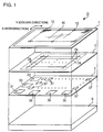
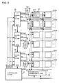
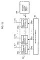
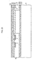
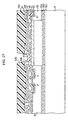
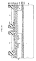
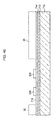
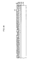
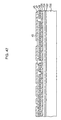
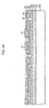
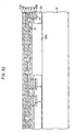
- Fig. 1 is a perspective view illustrating an electro-optical device according to an embodiment of the present invention.
- the electro-optical device D comprises a support substrate 6, an organic EL layer 1, a wire-forming layer 2, and an electronic component layer 3.
- the support substrate 6 is plate-shaped or film-shaped member made of glass, plastic, metal, ceramic, etc.
- the electronic component layer 3 is provided on one surface of the support substrate 6.
- the wire-forming layer 2 is provided on the opposite side of the support substrate 6 as seen from the electronic component layer 3, and the organic EL layer 1 is provided on the opposite side of the support substrate 6 as seen from the wire-forming layer 2.
- the organic EL layer 1 includes a plurality of organic EL elements 10 as electro-optical elements. These organic EL elements 10 are arranged in a matrix shape along in a row direction (X direction) and in a column direction (Y direction). The respective organic EL elements 10 are light emitting elements (elements to be driven) driven by the supplied current. The light emitted from the respective organic EL elements 10 are emitted toward an upper side in Fig. 1 (that is, in a direction opposite to the support substrate 6). Furthermore, this embodiment assumes that m organic EL elements 10 are arranged in the column direction and n organic EL elements 10 are arranged in the row direction. Accordingly, the total number of pixels is "m ⁇ n".
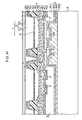
- the electronic component layer 3 includes a plurality of electronic components for driving the respective organic EL elements 10.
- the electronic component layer 3 includes various electronic components, such as semiconductor integrated circuits (IC chip) employing CMOS (Complementary Metal-Oxide Semiconductor) type or bipolar type of transistors, passive elements such as resistors or capacitors, TFT chips, or plate-shaped paper cells, and the like.
- IC chip semiconductor integrated circuits
- CMOS Complementary Metal-Oxide Semiconductor
- the electronic component layer 3 in this embodiment includes a controlling IC chip 31, a plurality of scanning IC chips 33, a plurality of column data-converting IC chips 35, and a plurality of pixel-driving IC chips 37 as the electronic components.
- the wire-forming layer 2 is located between the electronic component layer 3 and the organic EL layer 1.
- the wire-forming layer 2 includes a plurality of wires. Specifically, the wire-forming layer 2 has wires for connecting the electronic components included in the electronic component layer 3 each other.
- the wire-forming layer 2 includes a plurality of scanning-control line groups YL and a plurality of data lines DL.
- the respective scanning-control line groups YL are wires for electrically connecting the respective scanning IC chips 33 with the plurality of pixel-driving IC chips 37.
- the respective data lines DL are wires for electrically connecting the respective column data-converting IC chips 35 with the plurality of pixel-driving IC chips 37.
- the wire-forming layer 2 includes wires for connecting the electronic components included in the electronic component layer 3 with the organic EL elements 10 included in the organic EL layer 1.
- the wire-forming layer 2 includes wires (not shown in Fig. 1) for electrically connecting one pixel-driving IC chip 37 with the plurality of organic EL elements 10.
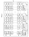
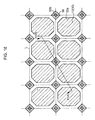
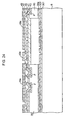
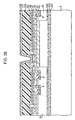
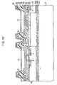
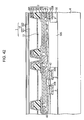
- a specific configuration of the electronic component layer 3 will be described with reference to Fig. 2.
- a plurality of pixel-driving IC chips 37 are arranged in a matrix shape along the row direction (X direction) and the column direction (Y direction).
- Each of the pixel-driving IC chips 37 is provided to each of the predetermined number of organic EL elements 10 in a plurality of organic EL elements 10 included in the organic EL layer 1.
- the corresponding relationship between the pixel-driving IC chips 37 and the organic EL elements 10 is as follows.
- a total of "m ⁇ n" organic EL elements 10 included in the organic EL layer 1 are classified into a plurality of groups (hereinafter, referred to as "element groups").
- the n organic EL elements 10 arranged in the row direction are divided into groups of q elements
- the m organic EL elements 10 arranged in the column direction are divided into groups of p elements, and so one element group consists of "p ⁇ q" organic EL elements 10 belonging to one area.
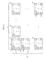
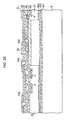
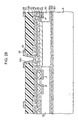
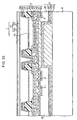
- one pixel-driving IC chip 37 is assigned to the respective element groups. That is, as shown in Fig. 3, the respective pixel-driving IC chips 37 are arranged to face the "p ⁇ q" organic EL elements 10 belonging to one element group, and serve for driving these organic EL elements 10.
- the plurality of scanning IC chips 33 are arranged in the column direction along one or two edges of the support substrate 6.
- the respective scanning IC chips 33 have a circuit for sequentially selecting the IC chips for driving the organic EL elements 10 from the plurality of pixel-driving IC chips 37.
- the plurality of column data-converting IC chips 35 are arranged in the row direction along other edges of the support substrate 6.
- the respective column data-converting IC chips 35 control currents flowing through the respective organic EL elements 10 on the basis of data (hereinafter, referred to as "image data") Xd indicative of images.
- the image data Xd are data for designating brightness (gray scale) of each organic EL element 10.
- the controlling IC chip 31 is arranged in a portion (that is, a corner portion of the support substrate 6) in which the column of the plurality of scanning IC chips 33 and the row of the plurality of column data-converting IC chips 35 intersect.
- the controlling IC chip 31 synthetically controls the respective scanning IC chips 33 and the respective column data-converting IC chips 35.
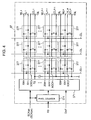
- the controlling IC chip 31 is connected to external apparatuses (not shown), such as a computer system, and receives the image data Xd or the control signal (for example, clock signals) for defining the timing of display operations from the external apparatuses.
- the controlling IC chip 31 comprises a display memory 31a.
- the display memory 31a is means for temporarily memorizing the image data Xd supplied from the external apparatuses.
- the controlling IC chip 31 generates signals (a reset signal RSET, a clock signal YSCL and a chip-selecting clock signal YECL to be described later) for selecting the plurality of scanning IC chips 33 one by one on the basis of the control signals supplied from the external apparatuses, and then supplies the signals to the respective scanning IC chips 33 (see Fig. 5). Furthermore, the controlling IC chip 31 supplies the image data Xd stored in the display memory 31a to the respective column data-converting IC chips 35 (see Fig. 9).
- controlling IC chip 31 generates a compulsory off signal Doff for forcibly stopping operation of the respective pixel-driving IC chips 37, and outputs this signals to the respective pixel-driving IC chips 37 through the wires included in the wire-forming layer 2.
- the respective pixel-driving IC chips 37 include circuits for driving a plurality of organic E1 elements 10 assigned thereto. More specifically, as shown in Fig. 4, each of the pixel-driving IC chips 37 has a pixel decoder 371, a pixel counter 374, and a plurality of pixel circuits 377. Each of the pixel circuits 377 is arranged in a matrix shape to have one-on-one correspondence with each of the organic EL elements 10 belonging to one element group. Therefore, each of the pixel-driving IC chips 37 includes a total of "p ⁇ q" pixel circuits 377. Each of the pixel circuits 377 is a circuit for driving one organic EL element 10. Thus, the "p ⁇ q" organic EL elements 10 included in the organic EL layer 1 are driven by one pixel-driving IC chip 37.
- the q pixel circuits 377 arranged in the row direction are mutually connected through one word line WLi (i is an integer satisfying 1 ⁇ i ⁇ m), one holding control signal line Hli, and one light-emitting control signal line GCLi.
- One ends of the respective word lines WLi, the respective holding control signal lines Hli, and the respective light-emitting control signal lines GCLi are connected to the pixel decoder 371.
- the selecting signals XWi are supplied from the pixel decoder 371 to the q pixel circuits 377, which are arranged in row direction, through the word lines WLi
- the holding control signals Xhi are supplied from the pixel decoder 371 to the q pixel circuits 37 through the holding control signal lines Hli
- the light-emitting control signals XGCi are supplied from the pixel decoder 371 to the q pixel circuits 37 through the light-emitting control signal lines GCLi.
- the p pixel circuits 377 arranged in the column direction are connected to the column data-converting IC chips 35 through one data line DLj (j is an integer satisfying 1 ⁇ j ⁇ n).
- all the pixel circuits 377 included in one pixel-driving IC chip 37 are connected to the pixel decoder 371 through common test signal lines TSL. Based on such configuration, test signals TS are simultaneously supplied from the pixel decoder 371 to the respective pixel circuits 377 through the test signal lines TSL. As a result, the performance test for all the pixel circuits 377 is carried out at the same time.
- a specific configuration of the scanning IC chip 33 will be described with reference to Fig. 5. Further, hereinafter, for the convenience of explanation, a group comprising a plurality of ("n/q") pixel-driving IC chips 37 arranged in the row direction is referred to as a "pixel-driving IC chip group”.
- one scanning IC chip 33 is provided for every two (that is, two rows) pixel-driving IC chip groups.
- Each scanning IC chip 33 controls operation of the plurality of ("2n/q") pixel-driving IC chips 37 belonging to the two pixel-driving IC chip groups.
- one pixel-driving IC chip group is referred to as a "first pixel-driving IC chip group 370a”
- the other pixel-driving IC chip group is referred to as a "second pixel-driving IC chip group 370b”.
- Each scanning IC chip 33 is connected to two pixel-driving IC chips 37, which are assigned to the scanning IC chip 33, through scanning control line groups YLk (k is an integer satisfying 1 ⁇ k ⁇ r) included in the wire-forming layer 2.
- Each scanning control line group YLk includes a first local clock signal line LCak, a second local clock signal line LCbk, and a local reset signal line LRS. More specifically, each scanning IC chip 33 is connected to a plurality of pixel-driving IC chips 37, which belong to the first pixel-driving IC chip group 370a, through the first local clock signal line LCak.
- each scanning IC chip 33 is connected to a plurality of pixel-driving IC chips 37, which belong to the second pixel-driving IC chip group 370b, through the second local clock signal line LCbk. Furthermore, two scanning IC chips 33 adjacent to each other are electrically connected through the wires included in the wire-forming layer 2.
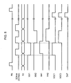
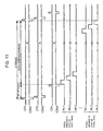
- Fig. 6 is a timing chart illustrating signal waveforms relating to the scanning of each pixel circuit 377.
- a reset signal RSET, a clock signal YSCL, and a chip-selecting clock signal YECL shown in Fig. 6 are signals supplied from the controlling IC chip 31 to each scanning IC chip 33.
- the reset signal RSET is a signal which defines a time period (hereinafter, referred to as "data writing period") for scanning all "m ⁇ n" organic EL elements 10, and rises to H level at a starting point of time of each data writing period.
- the clock signal YSCL is a signal which has a period corresponding to a time period of one horizontal scanning time.
- This horizontal scanning period corresponds to a time period when the n pixel circuits 377 in one row are selected at a time.
- the chip-selecting clock signal YECL is a signal for selecting a scanning IC chip 33, which actually controls the pixel-driving IC chips 37, among the plurality of scanning IC chips 33.
- the chip-selecting clock signal YECL rises to H level by "r" times corresponding to the number of scanning IC chips for one data writing period.
- Each scanning IC chip 33 sequentially outputs a first local clock signal SCKak and a second local clock signal SCKbk when it is selected by the chip-selecting clock signal YECL.
- the first local clock signal SCKak and the second local clock signal SCKbk are clock signals for selecting the plurality of pixel circuits 377 belonging to each pixel-driving IC chip group for every row.
- the k-th scanning IC chip 33 first outputs the first local clock signal SCKak to the plurality of pixel-driving IC chips 37 belonging to the first pixel-driving IC chip group 370a.
- the first local clock signal SCKak is a signal in which its level is changed at the same period as that of the clock signal YSCL, for a time period corresponding to the p horizontal scanning period, where p is the number of the pixel circuit 377 arranged in the column direction in the first pixel-driving IC chip group 370a.
- the scanning IC chip 33 selected by the chip-selecting clock signal YECL outputs the second local clock signal SCKbk to the plurality of pixel-driving IC chips 37 belonging to the second pixel-driving IC chip group 370b.
- the second local clock signal SCKbk is a signal of which the level is changed at the same period as that of the clock signal YSCL, for a time period corresponding to the p horizontal scanning period, where p is the number of the pixel circuit 377 arranged in the column direction in the second pixel-driving IC chip group 370b.
- the first local clock signal SCKak and the second local clock signal SCKbk are transmitted through the first local clock signal line LCak and the second local clock signal line LCbk, respectively.
- each scanning IC chip 33 when it is completed to select the pixel circuits 377 for p number of rows on the basis of the second local clock signal SCKbk, each scanning IC chip 33, as shown in Fig. 6, reverses the enable signal EOk, which will be output to the scanning IC chip 33 at a next stage, into H level.
- the enable signal EOk is a signal for notifying the scanning IC chip 33 at the next stage of that the scanning IC chip 33 has completed to select the pixel-driving IC chip group for two rows.
- the (k + 1)-th scanning IC chip 33, to which the enable signal EOk of H level is supplied, outputs a first local clock signal SCKak + 1 and a second local clock signal SCKbk + 1 in the same order as described above.
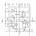
- Fig. 7 an electrical configuration of the pixel circuit 377 as a unit circuit will be described with reference to Fig. 7.
- Fig. 7 one pixel circuit 377 positioned in i-th row and j-th column is shown. This configuration is common to all the pixel circuits 377.
- the pixel circuit 377 comprises a plurality of MOS transistors and one capacitor C0. Specifically, the pixel circuit 377 has a pair of switching transistors Q1a and Q1b, a pair of reading-out transistors Q2a and Q2b, a capacitor C0, a light-emitting control transistor Q3, a test transistor Q8a and Q8b, and an analog memory portion 377a.
- the transistors Q1a, Q1b, Q2a, Q2b and Q3 are p channel MOS transistors, and the transistors Q8a and Q8b are n channel MOS transistors.
- the transistor Q2b is a driving transistor for supplying static current to the organic EL element 10
- the transistor Q3 is a transistor for controlling the pass and non-pass of the static current.
- the transistor Q1a is connected to the data line DLj and the transistor Q1b, and the gate terminal thereof is connected to the word line WLi. Furthermore, the transistor Q1b is connected to one end of the capacitor C0 and the transistor Q1a, and the gate terminal thereof is connected to the word line WLi. On the other hand, the other end of the capacitor C0 is connected to the power source line L1. A power source voltage VDD is applied to the power source line L1.
- the transistors Q2a and Q2b constitute a current mirror circuit. Specifically, the respective gate terminals of the transistors Q2a and Q2b are connected to one end of the capacitor C0. Furthermore, the transistor Q2a is connected to the transistor Q1a and the power source line L1. Therefore, when the selection signal XWi supplied through the word line Wli is transferred to L level, both of the transistors Q1a and Q1b become on state. In this way, when the transistor Q1b becomes on state, the transistor Q2b in which the gate terminal is connected to the drain terminal functions as a diode.
- the current corresponding to the data signal Dj of the data line DLj flows through a path of the power source line L1 ⁇ the transistor Q2a ⁇ the transistor Q1a ⁇ the data line DLj, and the electrical charge corresponding to the gate voltage of the transistor Q2a is accumulated in the capacitor C0.
- the transistor Q2b is connected to the source terminal of the transistor Q3 and the power source line L1.
- the transistor Q2b constitutes a current mirror circuit along with the transistor Q2a, and makes the electrical charge accumulated in the capacitor C0, that is, the current corresponding to the gate voltage of the transistor Q2b flowed to the transistor Q3.
- the gate terminal of the transistor Q3 is connected to the light-emitting control signal line GCLi. Furthermore, the drain terminal of the transistor Q3 is connected to the organic EL element 10 through the wire included in the wire-forming layer 2. Based on such configuration, when the light-emitting control signal XGCi is transferred to L level, the transistor Q3 becomes on state. At that time, the driving current Ie1 corresponding to the gate voltage of the transistor Q2b is supplied to the organic EL element 10 through the transistors Q2b and Q3. By means of supply of this driving current Ie1, the organic EL element 10 emits light.
- transistors Q2a, Q2b, and Q3 have been used as the transistors Q2a, Q2b, and Q3 in this embodiment, these transistors may be suitably replaced with n type transistors in accordance with the connection relationship of the organic EL element 10 or the power source line L1.
- the analog memory portion 377a is a circuit for keeping the electrical charge accumulated in the capacitor C0 constant.
- the analog memory portion 377a has transistors Q4a, Q4b, Q5, Q6, and Q7.
- the transistors Q4a and Q4b are n channel MOS transistors, and the transistors Q5, Q6 and Q7 are p channel MOS transistors.
- the transistors Q4a and Q4b constitute a current mirror circuit.
- the transistors Q5 and Q6 constitute a current mirror circuit.
- the transistor Q5 is connected to the power source line L1 and the transistor Q4a, and the gate terminal thereof is connected to one end of the capacitor C0.
- the transistor Q6 is connected to the power source line L1 and the transistor Q4b, and the gate terminal thereof is connected to the transistor Q7.
- the transistor Q7 is connected to one end of the capacitor C0 and the transistor Q6, and the gate terminal thereof is connected to the holding signal line HLi. Therefore, when the holding signal XHi becomes L level, the transistor Q7 becomes on state.
- the transistor Q4a is connected to the transistor Q5 and the earth line, and the gate terminal thereof is connected to the transistor Q5.
- the transistor Q4b is connected to the transistor Q6 and the earth line, and the gate terminal thereof is connected to the transistor Q5 and the gate terminal of the transistor Q4a.
- the analog memory portion 377a operates as follows. That is, when the electrical charge corresponding to the data signal is accumulated in the capacitor C0, the current corresponding to the gate voltage of the transistor Q2b flows from the transistor Q5 to the transistor Q4a.
- the transistors Q4a and Q4b constitute the equivalent times of current mirror circuit, the current equal to the current flowing through the transistor Q4a flows through the transistor Q4b, and the current flows through the transistor Q6.
- the transistor Q7 becomes on state, the gate voltage of the transistor Q6 is fed back to the capacitor C0 through the transistor Q7. As a result, the electrical charge accumulated in the capacitor C0 is constantly maintained.
- a nonvolatile memory circuit may be employed instead of the analog memory portion 377a.
- the analog memory portion 377a is a circuit useful for rapidly resuming display once the display is put-out for the purpose of a low power consumption or hot start of programs, it is not indispensable to the present invention.
- the pixel counter 374 shown in Fig. 4 is a means for sequentially specifying the pixel circuits 377 of each row included in one pixel-driving IC chip 37 with a purpose of selection.
- the local reset signal line LRS, and the first local clock signal line LCak or the second local clock signal line LCbk are connected to this pixel counter 374.
- the pixel counter 374 increases the count value by "1" whenever the first local clock signal SCKak or the second local clock signal SCKbk supplied from the scanning IC chip 33 rises to H level.
- the pixel counter 374 resets the count value to "0” whenever the local reset signal RS supplied from the scanning IC chip 33 rises to H level. Therefore, the count value by the pixel counter 374 increases by "1” for every horizontal scanning period from “0” up to "p", for one data writing period.
- the count value by the pixel counter 374 is output to the pixel decoder 371.
- the pixel decoder 371 is a means for sequentially selecting the pixel circuits 377 in each row included in one pixel-driving IC chip 37.
- the first local clock signal line LCak or the second local clock signal line LCbk is connected to the pixel decoder 371.
- the pixel decoder 371 simultaneously selects the plurality (q number) of pixel circuits 377 belonging to a row corresponding to the count value by the pixel counter 374. That is, the pixel decoder 371 controls the levels of the selection signal XWi, the holding control signal Xhi, and the light-emitting control signal XGCi as described below.
- the selection signal XWi is a signal which becomes L level for one horizontal scanning period in the data writing period. That is, the selection signal XWi is reversed to L level in synchronization with the i-th rise of the first local clock signal LCak or the second local clock signal LCbk, and is reversed to H level in synchronization with the (i + 1)-th rise, during the data writing period. Therefore, the selection signals XW1, XW2, ⁇ , XWp are sequentially reversed to L level in synchronization with the rise of the first local clock signal LCak or the second local clock signal LCbk.
- the holding control signal XHi is reversed to H level at a timing when the amount of a predetermined time elapses after the selection signal XWi falls to L level, and is reversed to L level after the time period corresponding to one horizontal scanning period elapses.
- the light-emitting control signal XGCi is a signal to which the level of the selection signal XWi is reversed. Therefore, the light-emitting control signals XGC1, XGC2, ⁇ , XGCp are sequentially reversed to H level in synchronization with the rise of the first local clock signal LCak or the second local clock signal LCbk.
- the gate terminals of the transistors Q8a and Q8b are connected to the test signal lines TSL.
- the drain terminal of the transistor Q8a is connected to the drain terminal of the transistor Q3.
- the transistor Q3 becomes off state in accordance with the compulsory off signal Doff, and the transistor Q8a becomes on state in accordance with the reversion of the test signal TS to H level.
- the anode layer of the organic EL element 10 is connected to the earth line through the transistor Q8a.
- the drain terminal of the transistor Q8b is connected to the data line DL.
- the transistor Q8b becomes on state.
- the data line DL is connected to the earth line through the transistor Q8b.
- the gate voltage of the transistor Q2a compulsorily is changed to the ground potential.
- the count value of the pixel counter 374 is set to plural values greater than "p", and the tests for contents assigned to the numerical values are carried out.
- p channel type transistors may be employed as the transistors Q8a and Q8b.
- each pixel circuit 377 will be described.
- this operation is common to all the pixel circuits 377.
- the transistors Q1a and Q1b of all the pixel circuits 377 belonging to the i-th row become on state.
- the current corresponding to the data signal Dj flows through the transistor Q2a, and the electrical charge corresponding to the current is accumulated in the capacitor C0.
- the light-emitting control signal XGCi is reversed to H level at the starting point of time of the horizontal scanning period
- the transistor Q3 becomes off state. Therefore, no current flows through the organic EL element 10 during charging the capacitor C0.
- the holding control signal XHi is reversed to H level at a timing when the amount of a predetermined time elapses after the selection signal XWi is reversed to L level, so that the transistor Q7 becomes off state.
- the transistors Q1a and Q1b of all the pixel circuits 377 belonging to the i-th row become off state.
- the transistors Q3 of all the pixel circuits 377 belonging to the i-th row become on state.
- the driving current Ie1 corresponding to the voltage held in the capacitor C0 is supplied to the organic EL element 10 through the transistors Q2b and Q3.
- the organic EL element 10 emits light with brightness corresponding to the magnitude of the driving current Ie1.
- the holding control signal XHi is reversed to L level at the point of time later in the amount of a predetermined time from the finishing point of time of the horizontal scanning period, the transistors Q7 of all the pixel circuits 377 belonging to the i-th row become on state. Therefore, the gate voltage of the transistor Q2b is constantly maintained by the analog memory portion 377a.
- the compulsory off signal Doff is supplied to the pixel decoder 371 from the controlling IC chip 31.
- the pixel decoder 371 reverses all the light-emitting control signals XGC1, XGC2, ⁇ , XGCp to H level.
- the transistors Q3 of all the pixel circuits 377 in the pixel-driving IC chip 37 become off state.
- all the organic EL elements 10 stop emitting light in accordance with the compulsory off signal Doff.
- the reset signal RSET supplied from the controlling IC chip 31 to the respective scanning IC chips 33 is at H level for a predetermined time period.
- Each scanning IC chip 33 sets the enable signal EOk, which will be supplied to the scanning IC chip 33 at the next stage, to L level, in synchronization with the rise of the reset signal RSET.
- each scanning IC chip 33 reverses the local reset signal RS supplied to the first pixel-driving IC chip group 370a and the second pixel-driving IC chip group 370b to H level for a predetermined time period.
- the pixel counter 374 included in each pixel-driving IC chip group resets the count value to "0".
- the first-stage scanning IC chip 33 is selected.
- This scanning IC chip 33 outputs a clock pulse of the first local clock signal SCKa1 on the basis of the clock signal YSCL supplied from the controlling IC chip 31.
- This first local clock signal SCKa1 is supplied to the first pixel-driving IC chip group 370a through the first local clock signal line LCa1.
- the pixel counter 374 of the pixel circuits 377 belonging to the first pixel-driving IC chip group 370a increases the count value from "0" to "1” in synchronization with the first rise of the clock pulse in the first local clock signal LCa1.
- the pixel decoder 371 selects the pixel circuits 377 in the first row corresponding to the count value "1", and carries out the operation (hereinafter, referred to as "selecting operation") for making the current corresponding to the data signal Dj flow to the organic EL elements 10 corresponding to these pixel circuits 377.
- the pixel decoder 371 reverses the selection signal XW1 corresponding to the count value "1" to L level for one horizontal scanning period.
- the transistors Q1a and Q2a of all the pixel circuits 377 belonging to the first row become on state. That is, all the pixel circuits 377 belonging to the first row are selected.
- the electrical charge corresponding to the current of the data signal Dj are charged in the capacitor C0.
- the pixel decoder 371 makes the transistors become off state by making the holding control signal XH1 be at H level, and makes the transistor Q3 become off state by making the light-emitting control signal XGC1 be at H level.
- the pixel decoder 371 reverses the selection signal XW1 to H level. As a result, the transistors Q1a and Q1b become off state in all the pixel circuits 377 belonging to the first row. Furthermore, the pixel decoder 371 reverses the holding control signal XH1 to L level at a little later timing slightly delayed from the rise of the selection signal XW1. As a result, the transistors Q7 of the pixel circuits 377 belonging to the first row become on state.
- the pixel decoder 371 reverses the light-emitting control signal XGC1 to L level at the same time of the rise of the selection signal XW1. As a result, the transistors Q3 of the pixel circuits 377 belonging to the first row become on state.
- the current Ie1 corresponding to the voltage held in the capacitor C0 flows between the sources and the drains of the transistors Q2b in all the pixel circuits 377 belonging to the first row. Therefore, the organic EL elements 10 emit light with the brightness (gray scale) corresponding to the data signal Dj.
- the pixel counter 374 increases the count value from "1" to "2".
- the same selecting operation as described above is carried out for the pixel circuits 377 in the second row belonging to the first pixel-driving IC chip group 370a.
- the same selecting operation as described above is carried out for the pixel circuits 377 in the p-th row belonging to the first pixel-driving IC chip group 370a. That is, whenever the pixel counter 374 increases the count value by "1" at the starting point of time of each horizontal scanning period, the selecting operation is carried out for the pixel circuits 377 in the row specified by the count value.
- the pixel circuits 377 in the k-th row belonging to the first pixel-driving IC chip group 370a are selected, and the organic EL elements 10 corresponding to these pixel circuits 377 emit light with the brightness in accordance with the data signal Dj.
- the first-stage scanning IC chip 33 outputs the clock pulse of the second local clock signal SCKb1 on the basis of the clock signal YSCL.
- the second local clock signal SCKb1 is supplied to the second pixel-driving IC chip group 370b through the second local clock signal line LCb1.
- the same selecting operation as described above is repeated for the first pixel-driving IC chip group 370a.
- the respective rows of the pixel circuits 377 belonging to the second pixel-driving IC chip group 370b are selected for every horizontal scanning period, and the organic EL elements 10 corresponding to the pixel circuits 377 emit light with the brightness in accordance with the data signal Dj.
- the first-stage scanning IC chip 33 reverses the enable signal EO1 supplied to the second-stage scanning IC chip 33 to H level.
- the aforementioned selecting operation is sequentially carried out for the first pixel-driving IC chip group 370a (the pixel-driving IC chips 37 in the third row) and the second pixel-driving IC chip group 370b (the pixel-driving IC chips 37 in the fourth row) corresponding to the second-stage scanning IC chip 33.
- the scanning IC chip 33 is selected by the chip-selecting clock signal YECL and the enable signal EO, and the same selecting operation as described above is sequentially carried out for the first pixel-driving IC chip group 370a and the second pixel-driving IC chip group 370b corresponding to the selected scanning IC chip 33.
- the selecting operation is sequentially carried out for the pixel circuits 377 in the p-th row belonging to the first pixel-driving IC chip group 370a (the pixel-driving IC chip group in the (2k - 1)-th row).
- the selecting operation is sequentially carried out for the pixel circuits 377 in the p-th row belonging to the second pixel-driving IC chip group 370b (the pixel-driving IC chip group in the (2k)-th row) corresponding to the k-th-stage scanning IC chip 33.
- the image corresponding to the image data Xd supplied from the external apparatus is displayed.
- the construction has been exemplified in Fig. 5 that one scanning IC chip 33 controls the pixel-driving IC chips 37 of two rows, the number of pixel-driving IC chips 37 assigned to the one scanning IC chip 33 is not limited thereto.
- each column data-converting IC chip 35 As shown in Fig. 2, according to this embodiment, one column data-converting IC chip 35 is provided to every group of the pixel-driving IC chips 37 in a plurality of columns (herein, referred to as "s" columns).
- the respective column data-converting IC chips 35 supply the data signals Dj to the pixel circuits 377 included in the pixel-driving IC chips 37 through the data lines DLj.
- the respective column data-converting IC chips 35 have an enable control circuit 351, a first latch circuit 353, a second latch circuit 354, a D/A converting circuit 356, and a standard-current supply circuit 358. Furthermore, although only the configuration of the first-stage column data-converting IC chip 35 is shown in detail in Fig. 9, the column data-converting IC chips 35 of the second or latter stages have the same configuration.
- the data control line LXD includes an enable signal line LXECL, an image data signal line LXd, a clock signal line LXCL, a reference current control line LBP, and a latch pulse signal line LLP.
- the enable signal line LXECL is a wire for supplying the enable control signal XECL from the controlling IC chip 31 to the enable control circuit 351 in the first-stage column data-converting IC chip 35.
- the enable control circuit 351 generates an enable signal EN based on the enable control signal XECL.
- the enable signal EN allows the first latch circuit 353 and the standard-current supply circuit 358 to operate or not to operate.
- the enable signal EN generated by the enable control circuit 351 is output to the input terminals of AND gates 353a, 353b and 359.
- the enable control circuit 351 in each column data-converting IC chip 35 is cascade-connected to the enable control circuit 351 in the next-stage column data-converting IC chip 35. Based on this configuration, the enable control circuits 351 in the column data-converting IC chips 35 of the second or latter stages receive the enable signal EN from the enable control circuits 351 of the previous-stage column data-converting IC chips 35, respectively, and generate the enable signal EN on the basis of the signal.
- the output terminal of the AND gate 353a and the output terminal of the AND gate 353b are connected to the first latch circuit 353.
- the image data Xd is input from the controlling IC chip 31 to the input terminal of the AND gate 353a through the image data signal line LXd. That is, the AND gate 353a outputs a logical product of the enable signal EN and the image data Xd to the first latch circuit 353. In other words, only in a time period when the enable signal EN is at H level, the image data Xd output from the controlling IC chip 31 is supplied to the first latch circuit 353 through the AND gate 353a.
- the clock signal XCL is input from the controlling IC chip 31 to the input terminal of the AND gate 353b through the clock signal line LXCL.
- the AND gate 353b outputs a logical product of the enable signal EN and the clock signal XCL to the first latch circuit 353.
- the clock signal XCL output from the controlling IC chip 31 is supplied to the first latch circuit 353 through the AND gate 353b.
- the clock signal XCL is a so-called dot clock.
- the enable signal EN is reversed to L level at a point of time when the image data Xd for the "s" pixel circuits 377 are taken in the first latch circuit 353. Therefore, the first latch circuit 353 accepts the image data Xd for the "s" pixel circuits 377.
- the output terminal of the first latch circuit 353 is connected to the input terminal of the second latch circuit 354.
- the output terminal of the second latch circuit 354 is connected to the input terminal of the D/A converting circuit 356.
- the latch pulse signal LP is input from the controlling IC chip 31 to the second latch circuit 354 through the latch pulse signal line LLP.
- the latch pulse signal LP is a signal which is reversed to H level at the starting point of the horizontal scanning period.
- the second latch circuit 354 simultaneously accepts the image data Xd for the "s" pixel circuits 377 held in the first latch circuit 353 at the rise of the latch pulse signal LP, and outputs the accepted image data Xd to the D/A converting circuit 356. That is, the first latch circuit 353 and the second latch circuit 354 carry out a serial/parallel conversion.
- the D/A converting circuit 356 is a circuit for outputting the current corresponding to the image data output from the second latch circuit 354 to the "s" data lines as the data signal Dj. That is, the D/A converting circuit 356 converts the image data Xd output from the second latch circuit 354 into an analog data signal Dj, and then outputs the analog data signal Dj to the data lines DLj.
- the D/A converting circuit 356 of this embodiment converts the image data Xd into the data signal Dj on the basis of the standard current Ir supplied from the standard-current supply circuit 358.
- the output terminal of the AND gate 359 is connected to the standard-current supply circuit 358.
- the standard current writing signal BP is input from the controlling IC chip 31 to the input terminal of the AND gate 359 through the reference current control line LBP.
- the AND gate 359 computes the logical product of the enable signal EN and the standard current writing signal BP, and outputs the result as the control pulse signal CP.
- the standard current writing signal BP output from the controlling IC chip 31 is supplied to the standard-current supply circuit 358 through the AND gate 359 as the control pulse signal CP.
- the standard current writing signal BP is a signal for instructing the standard-current supply circuit 358 to generate the standard current Ir.
- the approval or disapproval of the accepting operation of the image data Xd by the first latch circuit 353, and the approval or disapproval of the generating operation of the standard current Ir by the standard-current supply circuit 358 are controlled by the common enable signal EN.
- the approvals or disapprovals of the operations are controlled by separate signals.
- Fig. 10 is a view illustrating the configuration of the standard-current supply circuit 358 in the respective column data-converting IC chips 35. Furthermore, although only the standard-current supply circuits 358 included in the first-stage and second-stage column data-converting IC chips 35 are shown in Fig. 10, the standard-current supply circuits 358 of other column data-converting IC chips 35 have the same configuration.
- first-stage standard-current supply circuit 358 included in the first-stage column data-converting IC chip 35
- second-or-latter-stage standard-current supply circuits 358 are simply referred to as “second-or-latter-stage standard-current supply circuits 358”.
- the respective standard-current supply circuits 358 have a static current source 3581, a capacitor C1, and first to fourth switching means SW1 to SW4. Furthermore, the respective standard-current supply circuits 358 have transistors Tsw, T1, T2, T3, and Tm.
- the transistors Tsw, T1, T2, and Tm are n channel type FETs (Field Effect Transistors).
- the transistor T3 is a p channel type FET.
- the configurations of the second-or-latter-stage standard-current supply circuits 358 are the same as that of the first-stage standard-current supply circuit 358.
- the second-or-latter-stage standard-current supply circuits 358 and the first-stage standard-current supply circuit 358 have different connection condition for the fourth switching means SW4. That is, in the first-stage standard-current supply circuit 358, the power source potential of high potential (VDD) is applied to the gate terminal of the transistor Tsw and the fourth switching means SW4. Therefore, in the first-stage standard-current supply circuit 358, the transistor Tsw is always in on state, and the drain terminal of the transistor Tm is always connected to one end of the first switching means SW1 through the fourth switching means SW4.
- the power source potential of low potential (ground potential) is applied to the gate terminal of the transistor Tsw and the fourth switching means SW4. Therefore, in the second-or-latter-stage standard-current supply circuits 358, the transistor Tsw is always in off state, and the drain terminal of the transistor Tm is always disconnected from one end of the first switching means SW1. Thus, in the second-or-latter-stage standard-current supply circuits 358, the static current source 3581, the transistor T1, and the transistor Tm do not participate in operation.
- the static current source 3581 generates a static current Io and supplies the static current Io to the drain terminal of the transistor Tsw.
- the source terminal of the transistor Tsw is connected to the drain terminal of the transistor T1.
- the transistor T1 is diode-connected, and the source terminal thereof is connected to ground.
- the gate terminal of the transistor T1 is connected to the gate terminal of the transistor Tm. Therefore, the transistor T1 and the transistor Tm constitute a current mirror circuit. That is, the reference current Iref corresponding to the static current Io flowing through the transistor T1 flows in the transistor Tm.
- the source terminal of the transistor Tm is connected to ground.
- the drain terminal of the transistor Tm is connected to one end of the first switching means SW1 through the fourth switching means SW4.
- the other end of the first switching means SW1 is connected to one end of the second switching means SW2 and the drain terminal of the transistor T3.
- the other end of the second switching means SW2 is connected to the gate terminal of the transistor T3.
- One end of the capacitor C1 is connected to the gate terminal of the transistor T3.
- the other end of the capacitor C1 and the source terminal of the transistor T3 are connected to the power source line.
- drain terminal of the transistor T3 is connected to one end of the third switching means SW3.
- the other end of the third switching means SW3 is connected to the drain terminal of the transistor T2.
- the source terminal of the transistor T2 is earthed.
- first switching means SW1 and the second switching means SW2 are switched into any one of the on state and the off state in accordance with the control pulse signals CP (CP1, CP2, ⁇ ). More specifically, each of the first and second switching means SW1 and SW2 becomes on state when the control pulse signal CP is at H level, and becomes off state when the control pulse signal CP is at L level.
- the third switching means SW3 is switched into any one of the on state and the off state in accordance with the control inverted-pulse signals CSW (CSW1, CSW2, ⁇ ).
- the control inverted-pulse signal CSW is a signal for reversing the level of the control pulse signal CP and then delaying the signal. That is, the control pulse signal CP is input to a gate circuit comprising a delay circuit 3586 and an NOR gate 3585, and the output signal from the gate circuit is supplied to the third switching means SW3 as the control inverted-pulse signal CSW. More specifically, as shown in Fig. 11, when the control pulse signal CP is at H level, the control inverted-pulse signal CSW is at L level.
- the third switching means SW3 is in off state.
- the control inverted-pulse signal CSW becomes H level at a little later point of time after the control pulse signal CP is reversed to L level. At that time, the third switching means SW3 is in on state.
- the control pulse signal CP is at H level, and the first and second switching means SW1 and SW2 are all in on state.
- the current having a magnitude proportional to the static current Io generated by static current source 3581 flows through the transistor Tm, and the first and second switching means SW1 and SW2, and the electrical charge corresponding to the current is accumulated in the capacitor C1.
- the third switching means SW3 is in off state, the current does not flow through the second transistor T2.
- the control pulse signal CP is reversed to L level
- the first and second switching means SW1 and SW2 are in off state
- the third switching means SW3 is in on state.
- the standard current Ir1 corresponding to the electrical charge accumulated in the capacitor C1 that is, the gate voltage of the transistor T3 flows through the transistor T3.
- the standard current Ir1 is supplied to the transistor T2.
- one end of the first switching means SW1 in the first-stage standard-current supply circuit 358 is connected to one ends of the fourth switching means SW4 in all the second-or-latter-stage standard-current supply circuits 358 through the standard current supply line Lr. Therefore, in the first-stage standard-current supply circuit 358, when the first and second switching means SW1 and SW2 are in off state, the reference current Iref is supplied to all the second-or-latter-stage standard-current supply circuits 358 through the standard current supply line Lr. In addition, the electrical charge corresponding to the reference current Iref supplied through the standard current supply line Lr is accumulated in the capacitor C1 in each of the second-or-latter-stage standard-current supply circuits 358.
- the reference current Iref proportional to the static current Io which is output from the static current source 3581 in one column data-converting IC chip 35, is supplied to the standard-current supply circuits 358 in other column data-converting IC chips 35. Therefore, the magnitudes of the standard current Ir used in all the column data-converting IC chips 35 are equal. Furthermore, other means (for example, nonvolatile memory having the same function as the capacitor C1) having a function of holding the standard current Ir may be employed instead of the capacitor C1 shown in Fig. 10.
- D/A converting circuit 356 in the first-stage column data-converting IC chip 35 is shown in Fig. 12, the D/A converting circuits 356 in other column data-converting IC chips 35 also have the same configuration.
- the D/A converting circuit 356 in each of the column data-converting IC chips 35 has the "s" D/A converting portions 356a corresponding to the number of data lines assigned to the column data-converting IC chip 35.
- the current Ir1 output from the standard-current supply circuit 358 is supplied to each of the "s" D/A converting portions 356a.
- Each D/A converting portion 356a receives the image data Xd corresponding to one pixel circuit 377 from the second latch circuit 354. Then, each D/A converting portion 356a converts the image data into the data signal Dj on the basis of the current Ir1, and outputs the resultant data signal Dj to the data line XLj.
- the image data Xd is a 6-bit data.
- Fig. 13 is a view illustrating the configuration of each D/A converting portion 356a.
- the D/A converting portion 356a has 6 transistors Trc1 to Trc6, and 6 transistors Ts1 to Ts6.
- each of the transistors Trc1 to Trc6 constitutes a current mirror circuit along with the transistor T2.
- each of the transistors Trc1 to Trc6 functions as a static current source for outputting a predetermined current value.
- the sizes of the respective transistors Trc1 to Trc6 are selected such that the output current ratio (Ia:Ib:Ic:Id:Ie:If) of the transistors Trc1 to Trc6 is 1:2:4:8:16:32.
- the drain terminals of the transistors Ts1 to Ts6 are connected to the transistors Trc1 to Trc6, respectively. Furthermore, the source terminals of the transistors Ts1 to Ts6 are connected to one data line XLj.
- each bit of the image data Xd output from the second latch circuit 354 are supplied to the transistors Ts1 to Ts6, respectively. Specifically, the least significant bit of the image data Xd is supplied to the transistor Ts1, the most significant bit of the image data Xd is supplied to the transistor Ts6.
- the transistors Ts1 to Ts6 are switched to any one of the on state and the off state in accordance with each bit of the image data supplied from the second latch circuit 354.
- the current output from the transistors Trc1 to Trc6 are selectively supplied to the data lines XLj in accordance with the states of the transistors Ts1 to Ts6.
- the current corresponding to the image data Xd flows through the data lines XLj as the data signal Dj.
- the current value of the data signal Dj can be selected from sixty four values. Therefore, the brightness of the organic El elements 10 can be controlled to sixty four gray scales in accordance with the six-bit image data Xd.
- the respective pixel circuits 377 are sequentially selected for one data writing period. Then, supplying the data signal Dj from the column data-converting IC chip 35 to the respective pixel circuits 377 is sequentially carried out for one frame (horizontal scanning period) in synchronization with the scanning of the pixel circuits 377. Furthermore, in this embodiment, as shown in Fig. 11, the charging of the capacitor C1 in the respective standard-current supply circuits 358 is sequentially carried out for each data writing period, that is, a portion of time period (hereinafter, referred to as "set-up period") in each frame. In addition, the display of images is executed in a period other than the period for supplying the data signal to the pixel circuits 377. That is, the display of image may be executed for both of the set-up period and the data writing period.
- the standard current writing signal BP to be supplied to the first-stage column data-converting IC chip 35, and the enable signal EN generated by the enable control circuit 351 are simultaneously reversed to H level. Accordingly, when the control pulse signal CP1 is transferred to H level, the first and second switching means SW1 and SW2 in the first-stage standard-current supply circuit 358 are in on state. On the other hand, as shown in Fig. 11, the control inverted-pulse signal CSW1 is reversed to L level in accordance with the reversion of level of the control pulse signal CP1. Therefore, the third switching means SW3 in the first-stage standard-current supply circuit 358 is in off state. As a result, the electrical charge corresponding to the static current Io supplied from the static current source 3581 is accumulated in the capacitor C1 in the first-stage standard-current supply circuit 358.
- the control pulse signal CP1 is reversed to L level. Accordingly, the first and second switching means SW1 and SW2 in the first-stage standard-current supply circuit 358 are in off state. In addition, at that time, the control inverted-pulse signal CSW1 is reversed to H level. Therefore, the third switching means SW3 in the first-stage standard-current supply circuit 358 is in on state. As a result, it is completed to charge the capacitor C1 in the first-stage standard-current supply circuit 358.
- the standard current writing signal BP to be supplied to the second-stage column data-converting IC chip 35, and the enable signal EN generated in the enable control circuit 351 in the column data-converting IC chip 35 are simultaneously reversed to H level. Accordingly, when the control pulse signal CP2 is reversed to H level, the first and second switching means SW1 and SW2 in the second-stage standard-current supply circuit 358 are in on state. In addition, at that time, the control inverted-pulse signal CSW2 is reversed to L level, and the third switching means SW3 in the second-stage standard-current supply circuit 358 is in off state.
- the reference current Iref which corresponds to the static current Io in the first-stage column data-converting IC chip 358, is supplied to the second-stage column data-converting IC chip 35 through the standard current supply line Lr. Then, the electrical charge corresponding to the reference current Iref is accumulated in the capacitor C1 in the second-stage column data converting IC chips 35.
- the control pulse signal CP2 is reversed to L level, and the control inverted-pulse signal CSW2 is reversed to H level. Accordingly, the first and second switching means SW1 and SW2 in the second-stage standard-current supply circuit 358 are in off state, and the third switching means SW3 is in on state. As a result, it is completed to charge the capacitor C1 in the second-stage standard-current supply circuit 358.
- the same operation as described above is executed in other column data-converting IC chips 35.
- the electrical charge corresponding to the reference current Iref supplied from the first-stage standard-current supply circuit 358 is accumulated in the capacitors C1 in all the second-or-latter standard-current supply circuits 358. That is, the reference current Iref supplied from the first-stage standard-current supply circuit 358 is sequentially supplied to the capacitors C1 of the respective standard-current supply circuits 358 in time division.
- a configuration in which one set-up period is provided to every plurality of frames may be employed.
- a configuration in which the capacitor C1 in each of the standard-current supply circuits 358 is charged for an interval period (a period of time corresponding to the flyback period of the line sequential scanning) when the D/A converting circuits 356 output the data signals Dj may be employed. That is, one set-up period may disperse in a plurality of frames or disperse in one frame time, but it is preferable that the charging of the capacitors C1 for the set-up period be executed in the flyback period.
- the column data-converting IC chips 35 output the data signals in synchronization with the scanning of the pixel circuits 377 in the respective rows. That is, in the respective column data-converting IC chips 35, the data signal Dj is generated using the standard current Ir (Ir1, Ir2, ⁇ ), which corresponds to the electrical charge of the capacitor C1 in the standard-current supply circuit 358, as a standard value, and the data signal Dj is supplied to the currently selected pixel circuits 377.
- Ir Ir1, Ir2, ⁇
- the D/A converting circuit 356 or the standard-current supply circuit 358 may be provided in the pixel-driving IC chip 37. By this configuration, the same advantages as described above can be also obtained.
- the stacked structure of the electro-optical device D and the manufacturing method thereof according to the present invention will be described.
- three kinds of electro-optical devices in which their manufacturing methods are different will be exemplified, and the stacked structures and the manufacturing methods of the respective electro-optical devices will be explained.
- the pixel-driving IC chip 37, the controlling IC chip 31, the scanning IC chip 33, and the column data-converting IC chip 35 are not specifically distinguished, these are called generically as "IC chips 30".
- the electronic component layer 3 includes a base layer 301, a metal layer 302, IC chips 30 and a filling layer 304.
- the IC chips 30 shown in Fig. 14 are the pixel-driving IC chips 37.
- the base layer 301 is a layer covering all of one surface of the support substrate 6, and is made of an insulating material such as silicon oxide, silicon nitride or silicon oxide-nitride.
- the base layer 301 is a layer for preventing impurities eluted from the support substrate 6 from being doped into the electronic components, such as the pixel-driving IC chips 37.
- the metal layer 302 is a layer provided on the base layer 301, and is made of metal, such as copper (Cu) or gold (Au).
- the metal layer 302 includes mount portions 302a and alignment marks 302b.
- the mount portions 302a are a layer for improving the adhesion of the IC chips 30 to the support substrate 6 and for shielding the incident light from the support substrate 6 toward the IC chips 30. Therefore, the mount portions 302a are provided to overlap the area in which the IC chips 30 should be disposed. By these mount portions 302a, the malfunction of the IC chips 30 due to irradiation of light can be prevented.
- the alignment marks 302b are marks for adjusting the position of the IC chips 30 relative to the support substrate 6 to a predetermined position.
- the IC chip 30 has a plurality of pads P which are the connection terminals. Each IC chip 30 is arranged on the mount portions 302a in a state in which the opposite side of the surface (hereinafter, referred to as "pad formed surface") on which the pads P are formed face the support substrate 6. A metal layer 30a is formed on the surface opposite to the pad formed surface in the IC chip 30, that is, the surface (hereinafter, referred to as "substrate surface”) facing the support substrate 6 in a state in which the IC chip 30 is mounted on the support substrate 6.
- Fig. 15 is a plan view illustrating the pad formed surface of a pixel-driving IC chip 37.
- the plural pads P provided in the pixel-driving IC chip 37 are divided into first pads P1 and second pads P2, which have different sizes.
- the second pads P2 are terminals for connecting the pixel-driving IC chip 37 to other IC chips (the controlling IC chip 31, the scanning IC chips 33, and the column data-converting IC chips 35) or the power source line.
- Each of the second pads P2 has a size enough to mechanically come in contact with the probe pins in testing the pixel-driving IC chip 37.
- each second pad P2 is a rectangle in which the lengths in the longitudinal and transverse directions are all about 70 ⁇ m to 100 ⁇ m.
- the first pads P1 are terminals for connecting the pixel-driving IC chip 37 to the organic EL elements 10.
- Each first pad P1 is smaller than the second pads P2.
- the plane shape of each first pad P1 is a rectangle in which the lengths in the longitudinal and transverse directions are all about 10 ⁇ m to 30 ⁇ m.
- the pixel-driving IC chips 37 of this embodiment have two kinds of pads having different sizes. Therefore, as compared with a case in which all pads P have the same size as the second pads, the area of the pad formed surface in each IC chip 30 can be reduced. Specifically, since a plurality of pixel-driving IC chips 37 is provided in one electro-optical device D, decreasing the sizes of the respective pixel-driving IC chips 37 can effectively contribute to decrease the whole size of the electro-optical device D. In order to obtain this advantage, it is preferable that the area of the first pad be 1/50 to 1/6 of the area of the second pad.
- the pads of the controlling IC chip 31, the scanning IC chips 33, and the column data-converting IC chips 35 have the same size as the aforementioned second pad. However, some or all pads of the IC chips may have the same size as the aforementioned first pad.
- the filling layer 304 is a layer provided between the respective IC chips 30. That is, the filling layer 304 is provided to fill in the difference in level between the surface of the support substrate 6 (more specifically, the surface of the base layer 301) and the pad formed surfaces of the IC chips 30.
- the filling layer 304 is made of materials having high heat radiation. Specifically, the filling layer 304 is made of metal, such as copper (Cu), nickel (Ni) or tin (Sn). Accordingly, since the thermal uniformity of the whole electro-optical device D improves, the problems due to heat can be solved.
- the wire-forming layer 2 includes a first insulating layer 41, a first wiring layer 43, a second insulating layer 45, a second wiring layer 47, an anode layer 49, a third insulating layer 50, a bank layer 52, a conductive layer 54, a barrier layer 56, and a cathode layer 58.
- the first insulating layer 41, the second insulating layer 45, and the third insulating layer 50 are made of materials containing inorganic silicon or organic materials having heat resistance of 300°C or more.
- At least the first insulating layer 41 of the insulating layers is made of one or plural materials selected from polyarylether group resin (for example, SiLK), arylether group resin, aromatic polymer, polyimide, fluorine-added polyimide, fluorine resin, benzocyclobutene, polyphenylene group resin, and polyparaphenylene group resin.
- the second insulating layer 45 and the third insulating layer 50 are made of the same materials as the first insulating layer 41, or TEOS (tetraethyloxysilane)/O 2 film or SiO 2 film referred to as spin on glass (SOG) film.
- the first insulating layer 41 and the second insulating layer 45 are made of insulating materials of low permittivity. According to this constitution, the cross-talk between wires can be suppressed.
- the first insulating layer 41 is a layer covering the whole surface of the support substrate 6 on which the IC chips 30 and the filling layer 304 are provided.
- Contact holes 41a are provided in the portions of the first insulating layer 41 which overlap with the pads P in each IC chip 30.
- the aperture size of each contact hole 41a is determined so that the pads P of each IC chip 30 is exposed through the contact holes 41a even if errors in manufacturing (position errors when the IC chips 30 are arranged or position errors when the contact holes 41a are provided) occur.
- the first pads and the second pads in the IC chips 30 have different sizes. Therefore, the aperture sizes of the contact holes 41a corresponding to the first pad are different from the aperture sizes of the contact holes 41a corresponding to the second pad.
- the contact hole 41a corresponding to the pad P1 is about 4 ⁇ m in width and about 4 ⁇ m in length.
- the size of the contact hole 41a corresponding to the pad P2 be about 60 ⁇ m in width and about 60 ⁇ m in length.
- the first wiring layer 43 is provided on the first insulating layer 41 and is electrically connected to the pads P of each IC chip 30 through the contact holes 41a.
- the first wiring layer 43 is made of a high conductive metal, such as aluminum (Al) or alloy containing Al.
- the first wiring layer 43 includes an anode wire 43a and a cathode power source line 43b.
- the anode wire 43a is connected to the anode layer 49.
- the cathode power source line 43b is connected to the cathode layer 58 in the organic EL element 10.
- the first wiring layer 43 includes the data lines DL for supplying the data signals Dj from the column data-converting IC chips 35 to the pixel circuits 377, or the data control lines LXD for supplying the data control signals XD (see Fig. 9) from the controlling IC chip 31 to the column data-converting IC chips 35.
- the second insulating layer 45 is provided to cover the surface of the first insulating layer 41 provided with the first wiring layer 43. Contact holes 45a are provided in the portions of the second insulating layer 45 which overlap with a part of the first wiring layer 43.
- the second wiring layer 47 is provided on the second insulating layer 45 and is electrically connected to the first wiring layer 43 through the contact holes 45a.
- the second wiring layer 47 is made of a high conductive metal similarly to the first wiring layer 43.
- the second wiring layer 47 in this embodiment has a stacked structure of a layer made of aluminum and a layer made of titanium (Ti). By this structure, since the aluminum layer is covered with the titanium layer, the oxidation of aluminum layer by the oxide used as the anode layer 49 can be avoided.
- the second wiring layer 47 includes the scanning control line group YL extending from the scanning IC chips 33 to the pixel-driving IC chips 37. Furthermore, the second wiring layer 47 includes wires for supplying the compulsory off signal Doff from the controlling IC chip 31 to the pixel-driving IC chips 37, or wires for supplying various signals (reset signal RSET, clock signal YSCL, and chip-selecting clock signal YECL) from the controlling IC chip 31 to the scanning IC chips 33.
- the wires for connecting the pixel-driving IC chips 37 with the column data-converting IC chips 35 in the second wiring layer 47 are formed to be orthogonal to the wires connecting the scanning IC chips 33 with the pixel-driving IC chips 37 in the first wiring layer 43.
- Fig. 16 is a plan view illustrating the configuration of the electro-optical device D.
- the cross-sectional view taken along a line XIVA-XIVB in Fig. 16 corresponds to Fig. 14.
- the power source lines L comprising the first wiring layer 43 and the second wiring layer 47 are provided among the organic EL elements 10 arranged in a matrix shape. Therefore, the plane shape of the power source lines L is a lattice shape.
- the anode layer 49 is provided on the second wiring layer 47.
- the anode layer 49 comprises anode portions 49a and interconnection portions 49b.
- the anode portions 49a are a layer formed right below the EL layer 13 to be described later. Therefore, the anode portions 49a are provided in the positions corresponding to a plurality of organic EL elements 10 and are arranged in a matrix shape.
- the interconnection portions 49b are a layer for connecting the anode layer 58 with the first wiring layer 43.
- the interconnection portions 49b are situated in between the respective organic EL elements 10. Specifically, as shown in Fig. 16, the interconnection portion 49b is provided between two organic EL elements 10 adjacent to each other in the oblique direction. Therefore, a plurality of interconnection portions 49b is arranged in a matrix shape. However, the interconnection portions 49b can be properly omitted in accordance with the current values used for driving the organic EL elements 10.
- the anode layer 49 is made of, for example, a compound of indium oxide and tin oxide (ITO: Indium Tin Oxide), or a compound of indium oxide and zinc oxide (In 2 O 3 -ZnO), or conductive materials having a high work function, such as gold (Au). Furthermore, since the light emitted from the organic EL elements 10 is output to an opposite side of the anode layer 49, it is not necessary for the anode layer 49 to have light transmission.
- ITO Indium Tin Oxide
- In 2 O 3 -ZnO Indium oxide and zinc oxide
- Au gold
- the third insulating layer 50 is provided to cover the second wiring layer 47 and the second insulating layer 45 provided with the anode layer 49.
- the third insulating layer 50 has pixel aperture portions 50a and cathode contact portions 50b.
- the pixel aperture portions 50a are opening portions corresponding to the anode portions 49a in the anode layer 49.
- the cathode contact portions 50b are opening portions corresponding to the interconnection portions 49b in the anode layer 49.
- the bank layer 52 is a layer covering the second insulating layer 45 on which the anode layer 49 and the second wiring layer 47 are formed.
- the bank layer 52 is made of, for example, organic resin materials, such as photosensitive polyimide, acryl, polyamide.
- the bank layer 52 is a layer for partitioning the organic EL elements 10 adjacent to each other. Therefore, the bank layer 52 has pixel aperture portions 52a opened correspondingly to the organic EL elements 10.
- the bank layer 52 of this embodiment has cathode contact portions 52b for electrically connecting the anode layer 49 to the second wiring layer 47. As shown in Fig. 16, the cathode contact portions 52b are opening portions corresponding to the interconnection portions 49.
- the conductive layer 54 is a layer for connecting a portion of the second wiring layer 47 with the cathode layer 58. Specifically, the conductive layer 54 extends from the surface of the bank layer 52 to the surface of the second wiring layer 47 through the cathode contact portions 52 and the cathode contact portions 50b of the third insulating layer 50.
- the conductive layer 54 is made of a high conductive metal, such as aluminum alloy.
- the barrier layer 56 is a layer for preventing oxidation of the conductive layer 54, and is provided to cover the conductive layer 54.
- the barrier layer 56 has a stacked structure of, for example, a layer made of titanium and a layer made of gold.
- the cathode layer 58 is provided on the EL layer 13 constituting the organic EL elements 10.
- the cathode layer 58 is electrically connected to the second wiring layer 47 through the barrier layer 56 and the conductive layer 54.
- the cathode layer 58 has a property (transparency) transmitting the light emitted from the organic EL elements 10.
- the cathode layer 58 is made of a material having a low work function.
- the cathode layer 58 has a stacked structure of a first film made of lithium fluoride (LiF) or barium fluoride and the like, a second film made of calcium (Ca), and a third film made of gold.
- the materials of the first film and the second film are selected from metal belonging to group II or group III of the periodic table, or alloys or compounds containing the metal.
- the third film is a film for decreasing the resistance of the first or second film.
- the materials of the third film include Pt, Ni or Pb as well as Au.
- the third film may be made of oxide containing In, Zn or Sn.
- the organic EL layer 1 includes an EL layer 13 and a sealing layer 15.
- the EL layer 13 is made of known EL materials. That is, the EL layer 13 has a structure obtained by stacking a hole injection layer, a hole transfer layer, a light emitting layer, an electron transfer layer, and an electron injection layer using the well-known technologies.
- the EL layer 13 is interposed between the anode layer 49 (anode portions 49a) and the cathode layer 58 included in the wire-forming layer 2. Based on this configuration, when current flows between the anode layer 49 and the cathode layer 58, light is emitted from the EL layer 13 by recombination of holes and electrons.
- the EL layer 13 may be made of any one of inorganic EL materials and organic EL materials. Furthermore, the organic EL materials include high molecular materials and low molecular materials.
- the sealing layer 15 is a layer for isolating the EL layer 13 from the exterior.
- the sealing layer 15 has light transmission property so that the light emitted from the EL layer 13 emanates to the outside.
- the sealing layer 15 has a structure obtained by stacking alternately a plurality of flattened resin layers 151 and a plurality of barrier layers 152.
- the flattened resin layers 151 are formed by polymerizing and hardening resin monomers of an acryl group or a vinyl group, or a resin oligomer.
- the barrier layers 152 are made of (metal) oxide, such as Al 2 O 3 , SiO 2 or nitride film.
- a protective member may adhere onto the sealing layer 15. Or, the protective member may adhere instead of the sealing layer 15 shown in Fig. 14.
- a plate-shaped (or film-shaped) member made of, for example, glass or hard plastic and having light transmission can be used as the protective member.
- the base layer 301 is formed on one surface of the support substrate 6.
- the base layer 301 is obtained by depositing silicon oxide using, for example, plasma CVD method.
- the thickness of the base layer 301 is about 100 nm to 300 nm.
- the metal layer 302 is formed on the base layer 301. That is, first of all, a metal film made of copper or gold is formed by the sputtering method to cover the hole surface of the base layer 301. Then, the metal film is pattered and etched using a photolithography technology. By doing so, as shown in Fig. 17, the metal layer 302 including the mount portions 302a and the alignment marks 302b is obtained.
- the respective IC chips 30 (herein, the pixel-driving IC chips 37) are arranged on the mount portions 302a.
- a high-precision bare chip mounter having a mount precision of ⁇ 5 ⁇ m or less is used for the arrangement of the IC chips 30. Furthermore, the relative positional relationship of the respective IC chips 30 and the support substrate 6 is adjusted through the observation of the alignment marks 302b.
- the following processes are carried out in advance for the respective IC chips 30. That is, on wafer before being divided into the IC chips 30 by dicing, a protective tape (not shown) adheres to the surface corresponding to the substrate surface.
- the protective tape is made of materials having UV curable property. Therefore, the protective tape adheres to the pad formed surfaces of the respective IC chips 30 provided on the mount portions 302a.
- the grinding process is carried out for the surface of the wafer corresponding to the pad formed surface of each IC chip 30.
- the respective IC chips 30 have a thickness suitable for the formation of the wire-forming layer 2. Specifically, the thickness of each of the IC chips 30 is 100 ⁇ m or less (more preferably, about 25 ⁇ m to 30 ⁇ m).
- the wafer is diced after the metal layer 30a is formed on the surface corresponding to the pad formed surfaces.
- a die bonding tape adheres instead of the metal layer 30a.
- the filling layer 304 is formed to fill in the gaps between the respective IC chips 30 arranged on the support substrate 6.
- the filling layer 304 is obtained by means of the electric field plating using the IC chip 30 as a mask.
- the filling layer 304 is formed to be thinner than each IC chip 30. Specifically, the filling layer 304 is formed to be thinner than the IC chips 30 by about 0.1 ⁇ m to 3 ⁇ m.
- the protective tape adhered to the substrate surface of each chip 30 is removed. Specifically, first, the UV ray is irradiated to the substrate surface of the IC chips 30. By doing so, the adhesive force of the protective tape decreased. Subsequently, by applying organic solvent to the substrate surface of the IC chips 30, the protective tape is completely removed.
- the first insulating layer 41 is formed to cover the whole surface of the support substrate 6 provided with the IC chips 30 and the filling layer 304. That is, an insulating film is first formed to cover the whole surface of the support substrate 6 by means of the plasma CVD method using TEOS/O 2 .
- the thickness of the insulating film is about 400 nm to 900 nm.
- the insulating film is flattened by means of the CMP (Chemical Mechanical Polishing) method. Further, the insulating film may be formed by applying and sintering insulating materials.
- the insulating film is obtained.
- the respective IC chips 30 are molded on the support substrate 6 through the above processes.
- the part of the insulating film corresponding to the pads P of the IC chips 30 is removed and thus the contact holes 41a are formed.
- These contact holes 41a are formed in a lump by means of the patterning process and the etching process using the photolithography technology.
- the first insulating layer 41 is obtained through the above processes. Furthermore, when the surfaces of the pads P are exposed through the contact holes 41a, the oxide films formed on the surfaces of the pads P are removed by means of the reverse sputtering.
- the first wiring layer 43 is formed on the first insulating layer 41. That is, a metal film is first formed to cover the first insulating layer 41.
- the metal film is obtained by depositing the aluminum alloy, for example, using the sputtering.
- the thickness of the metal film is about 300 nm to 500 nm.
- the metal film leads to the surfaces of the pads P of the IC chips 30 through the contact holes 41a.
- the patterning process and the etching process using the photolithography technology are carried out for the metal film.
- the first wiring layer 43 including the anode wires 43a and the cathode power source lines 43b is obtained.
- the first wiring layer 43 may be formed by using the inkjet technology. That is, by ejecting ink containing metal particles from the inkjet head onto the support substrate 6 and drying the ink with heat treatment, the first wiring layer 43 is obtained.
- the second insulating layer 45 is formed to cover the surface of the first insulating layer 41 on which the first wiring layer 43 is formed.
- the second insulating layer 45 is formed by means of the same method as the first insulting layer 41. That is, an insulating film is first formed by means of the plasma CVD method or the sputtering. The thickness of the insulating film is about 500 nm to 900 nm. When the flatness of the insulating film is not enough to form the anode, the surface of the insulating film is flattened by means of the CMP method.
- the contact holes 45a are formed in a lump on a portion of the insulating film overlapping a part of the first wiring layer 43, and thus the second insulating layer 45 is obtained.
- the contact holes 45a are formed in the overlapping portions with parts of the anode wires 43a or the cathode power source lines 43b.
- a metal film 701 constituting the second wiring layer 47 is formed to cover the whole surface of the second insulating layer 45.
- the metal film 701 can be formed by means of, for example, the sputtering, the vacuum deposition method, or the aforementioned inkjet method.
- the metal film 701 comprises, for example, a first film formed on the second insulating layer 45 and a second film covering the first film.
- the first film is formed of, for example, aluminum alloy of about 300 nm to 500 nm in thickness.
- the second film is formed of, for example, titanium of about 50 nm to 100 nm in thickness.
- an anode material film 702 covering the metal film 701 is formed.
- the anode material film 702 is formed to be about 50 nm to 150 nm thick by means of, for example, the sputtering.
- the anode layer 49 has the anode portions 49a positioned right below the EL layer 13, and the interconnection portions 49b positioned in the gaps among the organic EL elements 10.
- the third insulating layer 50 is formed. That is, first of all, the silicon oxide is deposited to be about 150 nm to 300 nm by means of the plasma CVD method. Then, the regions of the silicon oxide film corresponding to the pixel aperture portions 50a and the cathode contact portions 50b are selectively removed by means of the photolithography technology, and the third insulating layer 50 is formed. Furthermore, when selectively removing the silicon oxide film, the portions of the silicon oxide film positioned in the vicinity of edges of the support substrate 6 are removed.
- a resin film 705 constituting the bank layer 52 is formed.
- the resin film 705 is obtained by applying organic materials, such as photosensitive polyimide, acryl, and polyamide, and hardening the organic materials by heating.
- the thickness of the resin film 705 is about 1.0 ⁇ m to 3.5 ⁇ m.
- the resin film 705 is opaque in its finishing state to prevent the light emitted from the EL layer 13 from traveling toward the IC chips.
- the patterning process and the developing process using a photo-mask are carried out for the resin film 705, and thus the cathode contact portions 52b are opened.
- the interconnection portions 49b of the anode layer 49 are exposed.
- the portions of the resin film 705 positioned in the vicinity of the edges of the support substrate 6 are removed.
- a metal film 707 constituting the conductive layer 54 is formed.
- the metal film 707 is obtained by depositing metal, such as aluminum, using the sputtering.
- the thickness of the metal film 707 is about 300 nm to 500 nm.
- a metal film 708 constituting the barrier layer 56 is formed.
- the metal film 708 is obtained by stacking a very thin film made of titanium and a film made of gold having the thickness of about 5 nm to 15 nm.
- the metal film 708 is formed using, for example, the sputtering.
- the pattering process and the etching process using the photo-mask are carried out for the metal film 707 and the metal film 708.
- the conductive layer 54 and the barrier layer 56 are obtained.
- a black non-reflecting layer may be formed to cover the portions of the resin film 705 other than the cathode contact portions 52b.
- the non-reflecting layer is a layer having a low light reflectivity (that is, high light absorptance), and is made of, for example, oxide, such as CrO 3 , MnO 2 , Mn 2 O 3 , NiO, Pr 2 O 5 , or resin materials containing carbon particles.
- the pixel aperture portions 52a are provided above the anode portions 49a of the resin film 705.
- the bank shape is fixed by baking the resin film 705.
- the plasma process using 4-fluorine methane as a reaction gas is carried out for the bank layer 52, and thus lyophobic group is introduced into the surface thereof. By doing so, the surface of the bank layer 52 is lyophobic.
- the lyophobic group is not introduced into the third insulating layer 50 or the anode layer 49, the surfaces thereof are lyophillic.
- the EL layer 13 is formed in each of the pixel aperture portions 52a of the bank layer 52.
- the EL layer 13 is made of a high polymer material, for example, PEDO (polythiophene)/PSS or PAni (polyanine) is first applied as a hole injection layer.
- PEDO polythiophene
- PAni polyanine
- the solution in which the light-emitting material, such as polyparaphenylenevinyl (PPV) group, polyvinylcarbasol (PVK) group, or polyfluorine group, is dissolved is applied to overlap the hole injection layer.
- the surface of the third insulating layer 50 or the anode layer 49 is lyophillic, while the surface of the bank layer 52 is lyophobic. Therefore, the liquid of the EL layer 13 effectively stays in the pixel aperture portions 52a of the bank layer 52. Furthermore, when the EL layer 13 is made of the high molecular material, a simple method, such as the inkjet method, print, and spin coating method, can be used in its formation. On the other hand, when the EL layer 13 is made of the low molecular material, the evaporation method or the transfer method using a shadow mask can be used in its formation.
- the color display is possible.
- a color filter may be formed above the EL layer 13 emitting the white light.
- a configuration of emitting only monochromatic light may be employed.
- the cathode layer 58 is formed to cover the whole surface of the bank layer 52 and the EL layer 13. That is, the continuous vapor deposition is carried out in vacuum by means of a multi-chamber type (cluster tool type) of film formation apparatus.
- the cathode layer 58 having a stacked structure of a very thin fluoride film of alkali metal, such as BaF or LiF, a Ca film of about 10 nm to 20 nm thick, and an Au film of about 2 nm to 15 nm thick is formed.
- the cathode layer 58 is formed after the EL layer 13 has been made of an organic material having low heat resistance. Therefore, it is preferable that the cathode layer 58 be formed in a condition of a temperature as low as possible.
- the sealing layer 15 including a flattened resin layer 151 and a barrier layer 152 is formed.
- the monomer or the oligomer of resins such as aryl group or vinyl group
- the resins are coated on the cathode layer 58.
- the UV ray is irradiated to the resin layer.
- the resin layer is polymerized and hardened, and thus the aforementioned flattened layer 151 is obtained.
- a thin film of metal oxide such as Al 2 O 3 or SiO 2 , is formed on the flattened resin layer 151 by various film forming methods, and the barrier layer 152 is obtained.
- the flattened resin layer 151 and the barrier layer 152 are formed repeatedly.
- the sealing layer 15 in which the plural flattened resin layers 151 and the plural barrier layers 152 are stacked alternatively is obtained.
- the protective member adheres to the surface of the uppermost barrier layer 152.
- Fig. 33 the reference numerals common to the parts in Fig. 14 are marked to the parts identical to those of the electro-optical device D obtained by the first manufacturing method.
- the plane configuration of the electro-optical device D is as shown in Fig. 16.
- the electro-optical device D shown in Fig. 33 has the same configuration as the electro-optical device D shown in Fig. 14, except for the structure of the electronic component layer 3.
- the electronic component layer 3 of the electro-optical device D includes the filling layer 305, the light-shielding layer 306, the base layer 307, and the IC chips (herein, the pixel-driving IC chips 37).
- the filling layer 305 is provided on the whole surface of the support substrate 6 to fill in the gaps among the respective IC chips 30.
- the filling layer 305 is made of a material having high heat radiation. By doing so, since the thermal uniformity of the whole electro-optical device D increases, generation of defects due to heat can be suppressed.
- the filling layer 305 is made of a material in which the coefficient of linear expansion is close to that of the IC chip 30.
- the filling layer 305 is made of a heat-resistant resin material in which silica filler is doped, glass of low-melting point, oxide, or metal such as copper.
- the light-shielding layer 306 is provided on the filling layer 305 to cover the whole surface of the support substrate 6 including the regions in which the IC chips 30 are arranged.
- the light-shielding layer 306 is a layer for preventing the incident light from the support substrate 6 side from traveling toward the IC chips 30, and is made of, for example, a metal such as aluminum or copper. The malfunction of the IC chips 30 due to irradiation of light can be prevented by means of the light-shielding layer 306. Furthermore, when the filling layer 306 is made of a light-shielding conductive material, the light-shielding layer 306 can be omitted.
- the base layer 307 is provided on the light-shielding layer 306 to cover the whole surface of the support substrate 6.
- the base layer 307 is a layer for forming the wire-forming layer 2, and is made of, for example, silicon oxide.
- the stress generated in accordance with deformation of the filling layer 305 can be released by means of the base layer 307.
- Each of the respective IC chips 30 is arranged on the base layer 307 in a state that its substrate surface is opposite to the support substrate 6.
- the base layer 307 prevents impurities from infiltrating from the support substrate 6 or the filling layer 305 to the IC chips.
- the base layer 307 also electrically insulates the wires included in the wire-forming layer 2 from the light-shielding layer 306.
- a light peeling layer 712 is formed on the whole surface of a substrate 710.
- the substrate 710 is a plate-shaped member having light transmission, and is made of, for example, glass.
- the light peeling layer 712 is obtained by depositing amorphous silicon using the plasma CVD method.
- a metal layer 714 is formed on the light peeling layer 712.
- the metal layer 714 is obtained by depositing aluminum by means of, for example, the sputtering method. Thereafter, the patterning process and the etching process using a photo-mask are carried out for the metal layer 714. By doing so, the alignment marks for adjusting the positions of the respective IC chips 30 are formed.
- a resin film 716 is formed to cover the light peeling layer 712.
- the resin film 716 is a layer which would be the first insulating layer 41 in a subsequent process, and is made of a heat-resistant organic material.
- the resin film 716 is formed by means of the spin coating method or the painting, etc. In this process, the resin film 716 is in a semi-polymerized state and has adhesion.
- the thickness of the resin film 716 is about 0.1 ⁇ m to 5 ⁇ m.
- the respective IC chips 30 are arranged in predetermined positions on the resin film 716.
- the respective IC chips 30 are arranged on the resin film 716 in a state in which their pad formed surfaces face the substrate 710. Therefore, the pads P can be prevented from being damaged in subsequent processes.
- the relative positional relationship between each IC chip 30 and the substrate 710 is adjusted by observing the alignment marks of the metal layer 714.
- a high precision bare chip mounter having a mount precision of ⁇ 5 ⁇ m or less is used for the arrangement of the IC chips 30.
- the resin film 716 is baked and thus completely polymerized. By doing so, the adhesion between the resin film 716 and the respective IC chips 30 is improved.
- the base layer 307 covering the whole surface of the substrate 710 on which the IC chips 30 are arranged is formed.
- the base layer 307 is obtained by depositing SiO 2 using, for example, the plasma CVD method.
- the thickness of the base layer 307 is about 100 nm to 500 nm.
- the light-shielding layer 306 is formed to cover the whole surface of the base layer 307.
- the light-shielding layer 306 is obtained by depositing metal such as copper or aluminum using the sputtering method.
- a hard resin is filled in the gaps among the respective IC chips 30.
- This hard resin is, for example, a heat-resistant resin material in which silica filler is doped, or glass of low-melting point.
- the support substrate 6 adheres to the substrate surfaces of the IC chips 30 through the hard resin.
- the IC chips 30 are used as spacers for adjusting the space between the support substrate 6 and the substrate 710.
- the filling layer 305 is obtained by hardening the hard resin by heating.
- the excimer laser light R which is an ultraviolet ray
- the light peeling layer 712 is exploded. That is, hydrogen contained in the light peeling layer 712 is vaporized, and thus cracks are generated in the light peeling layer 712.
- the substrate 710 is peeled off by the light peeling layer 712.
- the metal layer 714 and the light peeling layer 712 are removed by means of an etching solution.
- the etching solution dissolves the metal layer 714 and the light peeling layer 712, but does not affect the resin film 716.
- the support substrate 6 is reversed such that the surface on which the IC chips 30 are provided is directed upward.
- the electronic component layer 3 of the electro-optical device D shown in Fig. 33 is formed.
- the pad formed surfaces of the respective IC chips 30 and the surface of the base layer 307 are positioned in almost the same plane.
- the patterning process and the etching process are carried out for the resin film 716 to obtain the first insulating layer 41.
- the subsequent manufacturing processes are similar to the first manufacturing method shown in Figs. 20 to 32.
- the power source line to which the power source potential of high potential or low potential is applied can be formed by means of a process separate from the process in which the first wiring layer 43 and the second wiring layer 47 are formed.
- a process of forming the power source line can be carried out just before the process of arranging the respective IC chips 30 in the second manufacturing method.
- the power source line 309 is formed on the resin film 716.
- profiles of the respective IC chips 30 to be arranged on the resin film 716 in the subsequent process are marked in dotted lines.
- the power source lines 309 are formed at position not overlapping the alignment marks of the metal layer 714, in regions other than the regions in which the respective IC chips 30 would be arranged.
- a conductive layer made of a conductive material, such as aluminum or copper, is first formed on the resin film 716.
- the conductive layer can be formed by means of, for example, the electroless plating, the sputtering or the inkjet technology.
- the patterning process and the etching process are carried out for the conductive layer to obtain the power source line 309 shown in Fig. 40.
- the respective IC chips 30 are arranged on the resin film 716, and then the light-shielding layer 306 and the base layer 307 are formed to cover the power source line 309 and the IC chips 30.
- the processes thereafter are as described above.
- the process of forming the power source line 309 can be carried out right after the respective IC chips 30 are arranged on the resin film 716. Furthermore, in the first manufacturing method described above or the third manufacturing method described later, the power source line 309 can be formed through the same procedure.
- Fig. 41 is a view illustrating the stacked structure of the electro-optical device D obtained by this manufacturing method.
- the power source lines 309 are situated between the base layer 307 and the first insulating layer 41.
- the power source lines 309 are connected to the first wiring layer 43 through the contact holes 41a provided in the first insulating layer 41.
- FIG. 42 the stacked structure of the electro-optical device D obtained by the third manufacturing method will be described.
- Fig. 42 the reference numerals common to the parts of Fig. 14 are marked to the parts identical to those of the electro-optical device D obtained by the first manufacturing method.
- the plane configuration of the electro-optical device D is as shown in Fig. 16.
- bumps (projected electrodes) 308 are formed on the pads P of the IC chips 30.
- the bumps 308 are made of metal, such as indium (In) or gold (Au).
- the bumps 308 are connected to the bumps 42.
- the bumps 42 are connected to the first wiring layer 43 through the contact holes 41a opened in the first insulating layer 41.
- the bumps 42 are made of metal, such as indium or gold, similarly to the bumps 308.
- an insulating layer 722 is formed to cover the whole surface of the substrate 720.
- the substrate 720 is a plate-shaped member having light transmission, and is made of, for example, glass.
- the insulating layer 722 is obtained by depositing SiO 2 using, for example, the plasma CVD method. Furthermore, when the flatness of the insulating layer 722 is not enough, the insulating layer 722 is flattened by the CMP method.
- a light peeling layer 724 is formed on the whole surface of the insulating layer 722.
- the light peeling layer 724 is obtained by depositing amorphous silicon using, for example, the plasma CVD method.
- an insulating film 726 is formed on the whole surface of the light peeling layer 724.
- the insulating film 726 is obtained by depositing SiO 2 using the plasma CVD method.
- the insulating film 726 is a layer which would be the third insulating layer 50 shown in Fig. 42.
- a conductive film 728 which would be the anode layer 49 is formed on the insulating film 726.
- the conductive film 728 is obtained by depositing a conductive material having a large work function, such as ITO, using the sputtering method.
- a conductive material having a large work function such as ITO
- a metal film 730 which would be the second wiring layer 47 is formed to cover the conductive film 728.
- the metal film 730 is obtained by stacking a layer made of aluminum, etc. on the surface of a layer made of titanium, etc.
- the sputtering can be used to form the metal film 730.
- the patterning process and the etching process using a photo-mask are carried out for the conductive film 728 and the metal film 730 to obtain the anode layer 49 and the second wiring layer 47 shown in Fig. 42.
- the second insulating layer 45 is formed as shown in Fig. 46.
- the second insulating layer 45 is obtained by forming an insulating layer made of SiO 2 to cover the anode layer 49 and the second wiring layer 47 and then by patterning and etching the insulating layer using the photo-mask.
- the first wiring layer 43 is formed as shown in Fig. 47.
- the first wiring layer 43 is obtained by patterning and etching a metal layer made of aluminum formed by the sputtering.
- the first insulating layer 41 is formed as shown in Fig. 48. That is, first of all, an insulating film made of SiO 2 , etc. is formed to cover the first wiring layer 43. Then, the portions of the insulating film opposite to the pads P of the IC chips 30 are removed by means of the patterning process and the etching process to obtain the first insulating layer 41. Subsequently, as shown in Fig. 49, the bumps 42 are formed in the portions of the first wiring layer 43 opposite to the bumps 308 of the IC chips. The bumps 42 are formed to be about 0.5 ⁇ m to 5 ⁇ m thick by means of, for example, the lift off method. The bumps 42 are made of metal, such as indium or gold. When the bumps 42 are made of indium, their surfaces are covered with metal such as gold. By doing so, oxidation of the bumps 42 is prevented.
- the bumps 308 are formed on the pads P of the respective IC chips 30.
- the bumps 308 are made of metal, such as indium or gold.
- the thickness of the bumps 308 is about 2 ⁇ m to 10 ⁇ m.
- the respective IC chips 30 are arranged on the first insulating layer 41 in a state in which the bumps 308 of IC chips 30 are opposite to the bumps 42 on the first wiring layer 43.
- a high-precision bare chip mounter having mount precision of ⁇ 5 ⁇ m or less is used for the arrangement of the IC chips 30.
- the bumps 42 and the bumps 308 are heated in an instant. By doing so, the bumps 42 and the bumps 308 are bonded.
- a resin material is filled in the gaps among the respective IC chips 30.
- the resin material contains carbon particles to have the light-shielding properties.
- the support substrate 6 adheres to the substrate surfaces of the IC chips 30.
- the resin material filled among the IC chips 30 is hardened to obtain the filling layer 305.
- the excimer laser light R which is an ultraviolet ray
- the light peeling layer 724 is exploded, and the substrate 720 is peeled off by means of the light peeling layer 724 as shown in Fig. 52.
- the amorphous silicon remaining on the insulating film 726 is removed by means of the etching process.
- the patterning process and the etching process using a photo-mask are carried out for the insulating film 726 to obtain the third insulating layer 50 as shown in Fig. 42.
- the manufacturing processes thereafter are similar to the first manufacturing method shown in Figs. 26 to 32.
- the third manufacturing method can similarly apply to a case where active elements made from the low-temperature polysilicon are used in the electro-optical device D as well as for a case where the IC chips 30 including active elements are used in the electro-optical device.
- Fig. 53 is a perspective view illustrating a configuration of a personal computer as an example of the electronic apparatus according to the present invention.
- the personal computer 81 comprises a main body unit 812 including a keyboard 811 and a display unit 814 including the aforementioned electro-optical device D.
- the IC chips having various functions relating to the display of images can be included in the electronic component layer 3.
- Such kind of chips include, for example, IC chips having a display buffer memory or CPU, or IC chips having a data expanding function based on MPEG (Motion Picture Experts Group) or MP3 (MPEG Audio Layer-3), etc.
- MPEG Motion Picture Experts Group
- MP3 MPEG Audio Layer-3
- Fig. 54 is a perspective view illustrating a configuration of an electronic book as an example of the electronic apparatus according to the present invention.
- the electronic book 83 has a main body unit 830, a first display unit 831, and a second display unit 832.
- the main body unit 830 comprises a keyboard for receiving user's command.
- the first display unit 831 comprises the aforementioned electro-optical device D, that is, the electro-optical device D which displays images using the light-emission from the organic EL elements 10.
- the second display unit 832 comprises the electro-optical device D' which displays images using a plurality of pixels. However, the pixels in the second display unit 832 do not emit light by themselves.
- the non-emissive display such as an electrophoresis display, a reflective LCD (Liquid Crystal Display), a toner display, and a twist ball display, is used as the electro-optical device D' of the second display unit 832.
- the first display unit 831 is attached to an edge of the main body unit 830 through a hinge. Therefore, the first display unit 831 can rotate using the edge of the main body unit 830 as a shaft.
- the second display unit 832 is attached to an edge of the first display unit 831 opposite to the main body unit 830 through a hinge. Therefore, the second display unit 832 can rotate using the edge of the first display unit 831 as a shaft.
- the display by the first display unit 831 is executed by making the organic EL elements 10 emit light.
- the organic EL elements 10 in the first display unit 831 emit light with almost the same brightness.
- the light emitted from the first display unit 831 is reflected from the display surface of the second display unit 832 and then is observed by an observer. That is, the first display unit 831 functions not only as a display device, but also as an illuminating device (so-called front light) when images are displayed by the second display unit 832.
- the second display unit 832 is the non-emissive display, the illuminating device for securing the brightness of display does not need to be provided independently.
- the total thickness of the first display unit 831 and the second display unit 832 can be about 2 mm or less, the electronic book, which is thinner and lighter than a book using papers and has high performance, can be realized.
- the electronic apparatus to which the present invention can apply is not limited to the apparatuses shown in Figs. 53 and 54. That is, in addition to them, the present invention can apply to various apparatuses having the function of displaying images, such as a mobile phone, a game machine, an electronic paper, a video camera, a digital still camera, a car navigation apparatus, a car stereo apparatus, an operation manipulating panel, a printer, a scanner, a television, a video player, a pager, an electronic pocketbook, an electronic calculator, and a word processor.
- a mobile phone such as a mobile phone, a game machine, an electronic paper, a video camera, a digital still camera, a car navigation apparatus, a car stereo apparatus, an operation manipulating panel, a printer, a scanner, a television, a video player, a pager, an electronic pocketbook, an electronic calculator, and a word processor.
- the electro-optical device according to the present invention is not limited to a device for displaying images.
- the present invention may be applied to an image forming device using organic EL, LED or a field emission device (FED), or optical engine portion of an electro-photographic apparatus.
- the light corresponding to the image data is irradiated to a photosensitive body, such as a photosensitive drum, and toners are absorbed onto the latent image formed. Then, the toners are transcribed to a writing material such as paper.
- the electro-optical device according to the present invention can apply to a device for irradiating the light corresponding to the image data to the photosensitive body.
- this electro-optical device comprises light-emitting elements (electro-optical elements), each irradiating the light to the photosensitive body, and driving circuits for separately driving the respective light-emitting elements.
- a configuration in which a line exposure is possible correspondingly to a writing material having various widths such as A4 size or A3 size paper is employed. According to the electro-optical device of the present invention, it is possible to realize a thin and highly efficient printer or complex machine.
- the present invention can apply to the electro-optical device using the electro-optical elements, such as CCD (Charge Coupled Device) which outputs the current or voltage corresponding to the irradiated quantity of light.
- CCD Charge Coupled Device
- This electro-optical device is used as, for example, a light sensor array device (image pickup device) in a digital camera.
- a light sensor array device image pickup device
- Such type of light sensor array device is realized by providing the CCD instead of the organic EL elements 10 of the electro-optical device D according to the above embodiments and further providing the A/D converting circuits, which convert the analog signals output from the CCD into digital signals, instead of the D/A converting circuits 356.
- the electro-optical device used as a display device and the electro-optical device used as a light sensor array device are combined into a body. According to such device, the light-emitting brightness from the display device can be adjusted automatically in accordance with the peripheral brightness detected by the light sensor array device.
- the present invention can be applied to a device comprising elements other than the electro-optical elements. That is, the present invention may be applied to an element driving device comprising a plurality of driven elements (for example, arranged in the matrix shape) arranged at different positions in a plane, respectively, and unit circuits for driving the respective driven elements.
- an element driving device comprising a plurality of driven elements (for example, arranged in the matrix shape) arranged at different positions in a plane, respectively, and unit circuits for driving the respective driven elements.
- the driven elements for example, CCD of the aforementioned light sensor array
- This element driving device can be used as an input device, such as a touch panel or a thin keyboard, in various electronic apparatuses.
- the deviation in characteristics of the active elements can be suppressed in a circuit for driving the driven elements, such as the electro-optical elements.
Landscapes
- Physics & Mathematics (AREA)
- Engineering & Computer Science (AREA)
- General Physics & Mathematics (AREA)
- Theoretical Computer Science (AREA)
- Nonlinear Science (AREA)
- Multimedia (AREA)
- Optics & Photonics (AREA)
- Crystallography & Structural Chemistry (AREA)
- Chemical & Material Sciences (AREA)
- Human Computer Interaction (AREA)
- General Engineering & Computer Science (AREA)
- Mathematical Physics (AREA)
- Computer Hardware Design (AREA)
- Electroluminescent Light Sources (AREA)
- Devices For Indicating Variable Information By Combining Individual Elements (AREA)
- Liquid Crystal (AREA)
- Semiconductor Integrated Circuits (AREA)
- Photovoltaic Devices (AREA)
Applications Claiming Priority (15)
| Application Number | Priority Date | Filing Date | Title |
|---|---|---|---|
| JP2002156512 | 2002-05-29 | ||
| JP2002156512 | 2002-05-29 | ||
| JP2002316083 | 2002-10-30 | ||
| JP2002316083 | 2002-10-30 | ||
| JP2003038276 | 2003-02-17 | ||
| JP2003038276 | 2003-02-17 | ||
| JP2003042657 | 2003-02-20 | ||
| JP2003042657 | 2003-02-20 | ||
| JP2003112791 | 2003-04-17 | ||
| JP2003112791 | 2003-04-17 | ||
| JP2003146592A JP3551194B1 (ja) | 2002-05-29 | 2003-05-23 | 電気光学装置、その駆動回路、素子駆動装置および電子機器 |
| JP2003146592 | 2003-05-23 | ||
| JP2003146590A JP3551193B1 (ja) | 2002-05-29 | 2003-05-23 | 電気光学装置およびその製造方法、素子駆動装置およびその製造方法、素子基板ならびに電子機器 |
| JP2003146590 | 2003-05-23 | ||
| PCT/JP2003/006795 WO2003100753A1 (en) | 2002-05-29 | 2003-05-29 | Electrooptic device and production method therefor, element drive device and production method therefor, element substrate and electronic equipment |
Publications (2)
| Publication Number | Publication Date |
|---|---|
| EP1533779A1 true EP1533779A1 (de) | 2005-05-25 |
| EP1533779A4 EP1533779A4 (de) | 2008-03-26 |
Family
ID=29587969
Family Applications (1)
| Application Number | Title | Priority Date | Filing Date |
|---|---|---|---|
| EP03733185A Withdrawn EP1533779A4 (de) | 2002-05-29 | 2003-05-29 | Elektrooptische einrichtung und herstellungsverfahren dafür, elementansteuereinrichtung und herstellungsverfahren dafür, elementsubstrat und elektronisches gerüt |
Country Status (6)
| Country | Link |
|---|---|
| US (2) | US7183582B2 (de) |
| EP (1) | EP1533779A4 (de) |
| KR (3) | KR100633738B1 (de) |
| CN (1) | CN100430784C (de) |
| TW (1) | TWI230918B (de) |
| WO (1) | WO2003100753A1 (de) |
Cited By (3)
| Publication number | Priority date | Publication date | Assignee | Title |
|---|---|---|---|---|
| RU2460152C1 (ru) * | 2008-09-30 | 2012-08-27 | Шарп Кабушики Каиша | Дисплейная панель и способ контроля дисплейной панели |
| GB2571172A (en) * | 2017-12-29 | 2019-08-21 | Lg Display Co Ltd | Display apparatus |
| US12437703B2 (en) | 2021-02-12 | 2025-10-07 | Semiconductor Energy Laboratory Co., Ltd. | Display apparatus having pixel sets including light-emitting devices |
Families Citing this family (56)
| Publication number | Priority date | Publication date | Assignee | Title |
|---|---|---|---|---|
| US6965124B2 (en) * | 2000-12-12 | 2005-11-15 | Semiconductor Energy Laboratory Co., Ltd. | Light-emitting device and method of fabricating the same |
| JP4120279B2 (ja) * | 2002-06-07 | 2008-07-16 | セイコーエプソン株式会社 | 有機エレクトロルミネッセンス装置、有機エレクトロルミネッセンス装置の製造方法及び電子機器 |
| JP4413779B2 (ja) * | 2002-12-10 | 2010-02-10 | 株式会社半導体エネルギー研究所 | 発光装置およびその作製方法 |
| US20050253803A1 (en) * | 2004-05-13 | 2005-11-17 | Xerox Corporation | Electric paper display with a thin film transistor active matrix and integrated addressing logic |
| KR100578841B1 (ko) * | 2004-05-21 | 2006-05-11 | 삼성에스디아이 주식회사 | 발광 표시 장치와, 그 표시 패널 및 구동 방법 |
| JP4982663B2 (ja) * | 2004-06-25 | 2012-07-25 | 京セラ株式会社 | 表示パネル用ドライバ手段および画像表示装置 |
| JP4485277B2 (ja) * | 2004-07-28 | 2010-06-16 | 大日本印刷株式会社 | エレクトロルミネッセント素子の製造方法 |
| US7554589B2 (en) | 2004-08-20 | 2009-06-30 | Micron Technology, Inc. | Redundancy in column parallel or row architectures |
| JP4552804B2 (ja) * | 2004-11-08 | 2010-09-29 | セイコーエプソン株式会社 | 液滴吐出方法 |
| JP4428231B2 (ja) * | 2004-12-27 | 2010-03-10 | セイコーエプソン株式会社 | カラーフィルタ基板、電気光学装置、および電子機器 |
| JP4641820B2 (ja) * | 2005-02-17 | 2011-03-02 | 三洋電機株式会社 | 半導体装置の製造方法 |
| JP4885123B2 (ja) * | 2005-03-25 | 2012-02-29 | シャープ株式会社 | 半導体装置及びその製造方法 |
| KR100708863B1 (ko) * | 2005-12-09 | 2007-04-17 | 삼성에스디아이 주식회사 | 유기 발광 표시 장치 |
| US20100315387A1 (en) * | 2007-04-25 | 2010-12-16 | Panasonic Corporation | Plasma display device |
| DE102007040712B4 (de) * | 2007-08-23 | 2014-09-04 | Seereal Technologies S.A. | Elektronisches Anzeigegerät und Vorrichtung zur Ansteuerung von Pixeln eines Displays |
| US20100066683A1 (en) * | 2008-09-17 | 2010-03-18 | Shih-Chang Chang | Method for Transferring Thin Film to Substrate |
| GB0819450D0 (en) * | 2008-10-23 | 2008-12-03 | Cambridge Display Tech Ltd | Oled driver chiplet integration |
| US8796700B2 (en) * | 2008-11-17 | 2014-08-05 | Global Oled Technology Llc | Emissive device with chiplets |
| US7973472B2 (en) * | 2009-04-15 | 2011-07-05 | Global Oled Technology Llc | Display device with polygonal chiplets |
| US8259095B2 (en) * | 2009-08-20 | 2012-09-04 | Global Oled Technology Llc | Optically testing chiplets in display device |
| US8183765B2 (en) * | 2009-08-24 | 2012-05-22 | Global Oled Technology Llc | Controlling an electronic device using chiplets |
| GB0914816D0 (en) * | 2009-08-25 | 2009-09-30 | Isis Innovation | Method of fabrication of aligned nanotube-containing composites |
| WO2011034586A2 (en) | 2009-09-16 | 2011-03-24 | Semprius, Inc. | High-yield fabrication of large-format substrates with distributed, independent control elements |
| US8115383B2 (en) * | 2009-10-29 | 2012-02-14 | Global Oled Technology Llc | Electroluminescent area illumination with integrated mechanical switch |
| JP5056834B2 (ja) * | 2009-11-24 | 2012-10-24 | 大日本印刷株式会社 | エレクトロルミネッセント素子の製造方法 |
| JP5757083B2 (ja) | 2010-12-01 | 2015-07-29 | セイコーエプソン株式会社 | 薄膜トランジスタ形成用基板、半導体装置、電気装置 |
| US8599118B2 (en) * | 2011-02-16 | 2013-12-03 | Global Oled Technology Llc | Chiplet display with electrode connectors |
| US8791642B2 (en) * | 2011-03-03 | 2014-07-29 | Cree, Inc. | Semiconductor light emitting devices having selectable and/or adjustable color points and related methods |
| US8796952B2 (en) | 2011-03-03 | 2014-08-05 | Cree, Inc. | Semiconductor light emitting devices having selectable and/or adjustable color points and related methods |
| JP5966412B2 (ja) * | 2011-04-08 | 2016-08-10 | ソニー株式会社 | 画素チップ、表示パネル、照明パネル、表示装置および照明装置 |
| US20120314171A1 (en) * | 2011-06-08 | 2012-12-13 | Micron Technology, Inc. | Display devices having electrolessly plated conductors and methods |
| TWI522563B (zh) * | 2012-02-16 | 2016-02-21 | 陞泰科技股份有限公司 | 可變光束的發光二極體及其方法 |
| KR20140028459A (ko) * | 2012-08-29 | 2014-03-10 | 삼성전기주식회사 | 터치패널 |
| CN102916036B (zh) * | 2012-10-12 | 2015-05-13 | 京东方科技集团股份有限公司 | 一种有源矩阵有机电致发光显示器件及显示装置 |
| US9153171B2 (en) | 2012-12-17 | 2015-10-06 | LuxVue Technology Corporation | Smart pixel lighting and display microcontroller |
| US9924065B2 (en) | 2013-08-30 | 2018-03-20 | Kyocera Document Solutions Inc. | Lighting control circuit and image forming apparatus |
| WO2015162768A1 (ja) | 2014-04-24 | 2015-10-29 | ルネサスエレクトロニクス株式会社 | 半導体装置およびその製造方法 |
| KR102369088B1 (ko) * | 2015-01-29 | 2022-03-02 | 삼성디스플레이 주식회사 | 유기 발광 표시 장치 및 유기 발광 표시 장치의 제조 방법 |
| DE102015206840B4 (de) * | 2015-04-16 | 2024-08-08 | Bayerische Motoren Werke Aktiengesellschaft | Thermisch überwachte Ladevorrichtung |
| US10483253B1 (en) | 2015-09-24 | 2019-11-19 | Apple Inc. | Display with embedded pixel driver chips |
| US10665578B2 (en) | 2015-09-24 | 2020-05-26 | Apple Inc. | Display with embedded pixel driver chips |
| JP6597192B2 (ja) * | 2015-10-30 | 2019-10-30 | セイコーエプソン株式会社 | 電気光学装置、電子機器、及び電気光学装置の駆動方法 |
| CN109156065B (zh) * | 2016-05-18 | 2020-12-11 | 株式会社日本有机雷特显示器 | 有机el显示面板及其制造方法 |
| KR102632617B1 (ko) * | 2016-08-08 | 2024-02-02 | 삼성디스플레이 주식회사 | 마스크 조립체, 이를 이용한 표시 장치의 제조장치, 이를 이용한 표시 장치의 제조방법 및 표시 장치 |
| US10408896B2 (en) | 2017-03-13 | 2019-09-10 | University Of Utah Research Foundation | Spintronic devices |
| TWI630590B (zh) | 2017-07-05 | 2018-07-21 | Industrial Technology Research Institute | 畫素結構以及顯示面板 |
| US10847739B2 (en) * | 2017-09-21 | 2020-11-24 | Sharp Kabushiki Kaisha | Display device having larger openings on inner sides of anode electrodes in display region than on inner sides of anode electrodes in peripheral display region |
| US11073927B2 (en) | 2018-07-26 | 2021-07-27 | Apple Inc. | Touch sensing utilizing integrated micro circuitry |
| JP2020118924A (ja) * | 2019-01-28 | 2020-08-06 | セイコーエプソン株式会社 | 電気光学装置、表示制御システム、表示ドライバー、電子機器及び移動体 |
| CN111508968B (zh) * | 2019-01-30 | 2023-08-01 | 群创光电股份有限公司 | 基板修补方法及电子装置 |
| KR102228084B1 (ko) * | 2019-03-26 | 2021-03-16 | 주식회사 사피엔반도체 | 저전압 트랜지스터를 이용한 화소 및 이를 포함하는 마이크로 표시장치 |
| TWI718665B (zh) * | 2019-09-12 | 2021-02-11 | 世界先進積體電路股份有限公司 | 半導體裝置及其製造方法 |
| CN113990212A (zh) * | 2020-07-27 | 2022-01-28 | 北京芯海视界三维科技有限公司 | 发光模组及显示器件 |
| KR102903634B1 (ko) * | 2021-08-18 | 2025-12-29 | 삼성디스플레이 주식회사 | 표시 장치 및 이의 구동 방법 |
| KR20230069571A (ko) * | 2021-11-12 | 2023-05-19 | 엘지디스플레이 주식회사 | 표시장치 |
| CN116759426A (zh) * | 2022-03-04 | 2023-09-15 | 敦泰电子股份有限公司 | 薄膜晶体管感光电路、显示面板、使用其的行动装置以及其制造方法 |
Family Cites Families (35)
| Publication number | Priority date | Publication date | Assignee | Title |
|---|---|---|---|---|
| JP2748654B2 (ja) * | 1990-06-11 | 1998-05-13 | 松下電器産業株式会社 | 液晶表示用基板およびそれを用いた液晶表示装置 |
| JPH0740096B2 (ja) | 1990-12-18 | 1995-05-01 | セイコーエプソン株式会社 | 駆動装置 |
| JP2794499B2 (ja) * | 1991-03-26 | 1998-09-03 | 株式会社半導体エネルギー研究所 | 半導体装置の作製方法 |
| US5417025A (en) * | 1993-01-19 | 1995-05-23 | Armstrong World Industries, Inc. | Resiliently mounted accessible tile |
| JP3626521B2 (ja) | 1994-02-28 | 2005-03-09 | 三菱電機株式会社 | 基準電位発生回路、電位検出回路および半導体集積回路装置 |
| JP2643098B2 (ja) * | 1994-12-07 | 1997-08-20 | インターナショナル・ビジネス・マシーンズ・コーポレイション | 液晶表示装置及びその製造方法並びに画像形成方法 |
| JPH08184821A (ja) | 1994-12-28 | 1996-07-16 | Sharp Corp | 表示装置 |
| US5877735A (en) | 1995-06-23 | 1999-03-02 | Planar Systems, Inc. | Substrate carriers for electroluminescent displays |
| JP3373366B2 (ja) | 1996-08-07 | 2003-02-04 | シャープ株式会社 | 信号線選択回路およびマトリクス型表示装置 |
| US6372608B1 (en) * | 1996-08-27 | 2002-04-16 | Seiko Epson Corporation | Separating method, method for transferring thin film device, thin film device, thin film integrated circuit device, and liquid crystal display device manufactured by using the transferring method |
| JPH11183862A (ja) | 1997-12-22 | 1999-07-09 | Sanyo Electric Co Ltd | 液晶表示装置 |
| JPH11237845A (ja) | 1998-02-23 | 1999-08-31 | Toshiba Electronic Engineering Corp | 表示制御装置 |
| JP4298068B2 (ja) * | 1998-08-18 | 2009-07-15 | セイコーエプソン株式会社 | 電気光学装置およびそれらを備えた電子機器並びに電気光学装置の製造方法 |
| US6312304B1 (en) * | 1998-12-15 | 2001-11-06 | E Ink Corporation | Assembly of microencapsulated electronic displays |
| JP3462135B2 (ja) * | 1999-01-14 | 2003-11-05 | シャープ株式会社 | 二次元画像検出器およびアクティブマトリクス基板並びに表示装置 |
| JP3906599B2 (ja) | 1999-02-15 | 2007-04-18 | セイコーエプソン株式会社 | 組み合わせ基板の接合方法 |
| JP3025257B1 (ja) * | 1999-02-25 | 2000-03-27 | 松下電器産業株式会社 | 表示パネル |
| JP3500322B2 (ja) | 1999-04-09 | 2004-02-23 | シャープ株式会社 | 定電流駆動装置および定電流駆動半導体集積回路 |
| JP2001042827A (ja) | 1999-08-03 | 2001-02-16 | Pioneer Electronic Corp | ディスプレイ装置及びディスプレイパネルの駆動回路 |
| JP2001067048A (ja) | 1999-08-31 | 2001-03-16 | Hitachi Ltd | 液晶表示装置 |
| JP3633394B2 (ja) | 1999-09-13 | 2005-03-30 | セイコーエプソン株式会社 | 電気光学装置及び電子機器 |
| JP3911929B2 (ja) | 1999-10-25 | 2007-05-09 | セイコーエプソン株式会社 | 液晶表示装置の製造方法 |
| JP2001154613A (ja) | 1999-12-01 | 2001-06-08 | Avix Inc | パネル型led表示モジュール |
| JP2001196169A (ja) | 2000-01-14 | 2001-07-19 | Sharp Corp | 有機エレクトロルミネッセンス素子の製造方法 |
| JP3967081B2 (ja) | 2000-02-03 | 2007-08-29 | 株式会社半導体エネルギー研究所 | 発光装置及びその作製方法 |
| US6559594B2 (en) | 2000-02-03 | 2003-05-06 | Semiconductor Energy Laboratory Co., Ltd. | Light-emitting device |
| JP3812263B2 (ja) | 2000-02-09 | 2006-08-23 | セイコーエプソン株式会社 | 電気光学装置の駆動回路、電気光学装置および電子機器 |
| TWI226205B (en) * | 2000-03-27 | 2005-01-01 | Semiconductor Energy Lab | Self-light emitting device and method of manufacturing the same |
| JP4403631B2 (ja) | 2000-04-24 | 2010-01-27 | ソニー株式会社 | チップ状電子部品の製造方法、並びにその製造に用いる擬似ウエーハの製造方法 |
| JP2002108233A (ja) | 2000-09-29 | 2002-04-10 | Minolta Co Ltd | 表示装置 |
| JP2002134272A (ja) | 2000-10-25 | 2002-05-10 | Ricoh Co Ltd | エレクトロルミネセンス素子及びその作製方法 |
| US6417025B1 (en) | 2001-04-02 | 2002-07-09 | Alien Technology Corporation | Integrated circuit packages assembled utilizing fluidic self-assembly |
| JP2002318556A (ja) | 2001-04-20 | 2002-10-31 | Toshiba Corp | アクティブマトリクス型平面表示装置およびその製造方法 |
| JP2002318553A (ja) | 2001-04-20 | 2002-10-31 | Toshiba Corp | 自己発光型表示装置 |
| JP4095830B2 (ja) | 2002-01-29 | 2008-06-04 | 統寶光電股▲ふん▼有限公司 | 有機ledデバイスおよびその製造方法 |
-
2003
- 2003-05-27 US US10/445,079 patent/US7183582B2/en not_active Expired - Lifetime
- 2003-05-28 TW TW092114424A patent/TWI230918B/zh not_active IP Right Cessation
- 2003-05-29 KR KR1020047004157A patent/KR100633738B1/ko not_active Expired - Lifetime
- 2003-05-29 KR KR1020067018752A patent/KR100740162B1/ko not_active Expired - Lifetime
- 2003-05-29 KR KR1020067008566A patent/KR100690551B1/ko not_active Expired - Lifetime
- 2003-05-29 WO PCT/JP2003/006795 patent/WO2003100753A1/ja not_active Ceased
- 2003-05-29 CN CNB038017261A patent/CN100430784C/zh not_active Expired - Lifetime
- 2003-05-29 EP EP03733185A patent/EP1533779A4/de not_active Withdrawn
-
2006
- 2006-06-29 US US11/476,687 patent/US7364928B2/en not_active Expired - Lifetime
Cited By (5)
| Publication number | Priority date | Publication date | Assignee | Title |
|---|---|---|---|---|
| RU2460152C1 (ru) * | 2008-09-30 | 2012-08-27 | Шарп Кабушики Каиша | Дисплейная панель и способ контроля дисплейной панели |
| GB2571172A (en) * | 2017-12-29 | 2019-08-21 | Lg Display Co Ltd | Display apparatus |
| US10818241B2 (en) | 2017-12-29 | 2020-10-27 | Lg Display Co., Ltd. | Display apparatus |
| GB2571172B (en) * | 2017-12-29 | 2022-01-05 | Lg Display Co Ltd | Display apparatus |
| US12437703B2 (en) | 2021-02-12 | 2025-10-07 | Semiconductor Energy Laboratory Co., Ltd. | Display apparatus having pixel sets including light-emitting devices |
Also Published As
| Publication number | Publication date |
|---|---|
| WO2003100753A1 (en) | 2003-12-04 |
| US7183582B2 (en) | 2007-02-27 |
| EP1533779A4 (de) | 2008-03-26 |
| CN100430784C (zh) | 2008-11-05 |
| KR100633738B1 (ko) | 2006-10-13 |
| US20040032637A1 (en) | 2004-02-19 |
| KR100740162B1 (ko) | 2007-07-18 |
| CN1602509A (zh) | 2005-03-30 |
| KR20060064697A (ko) | 2006-06-13 |
| US7364928B2 (en) | 2008-04-29 |
| TW200407831A (en) | 2004-05-16 |
| KR20040039392A (ko) | 2004-05-10 |
| KR20060115921A (ko) | 2006-11-10 |
| KR100690551B1 (ko) | 2007-03-12 |
| US20060246619A1 (en) | 2006-11-02 |
| TWI230918B (en) | 2005-04-11 |
Similar Documents
| Publication | Publication Date | Title |
|---|---|---|
| US7364928B2 (en) | Electro-optical device and method of manufacturing the same, element driving device and method of manufacturing the same, element substrate, and electronic apparatus | |
| US7285033B2 (en) | Color filter, display device and electronic equipment, manufacturing method thereof, and apparatus for manufacturing display device | |
| US12198616B2 (en) | Pixel group and column token display architectures | |
| US12238991B2 (en) | Display substrate comprising sub-pixels in fan-out wiring region and preparation method therefor | |
| US20050017268A1 (en) | Display apparatus and its manufacturing method | |
| US12433116B2 (en) | Display substrate and display apparatus | |
| US12150369B2 (en) | Display panel, display device, test method and crack detection method | |
| JP4461710B2 (ja) | 電気光学装置及び電子機器 | |
| CN100520540C (zh) | 电光学装置、元件驱动装置和电子设备 | |
| JP3551193B1 (ja) | 電気光学装置およびその製造方法、素子駆動装置およびその製造方法、素子基板ならびに電子機器 | |
| US20240237449A1 (en) | Display Substrate and Display Apparatus | |
| JP3551194B1 (ja) | 電気光学装置、その駆動回路、素子駆動装置および電子機器 | |
| JP2005003698A (ja) | 電気光学装置、その駆動回路、素子駆動装置および電子機器 | |
| JP3876870B2 (ja) | 電気光学装置、その駆動回路、素子駆動装置および電子機器 | |
| JP4055688B2 (ja) | 電気光学装置の製造方法 | |
| US20240292654A1 (en) | Display Substrate and Display Apparatus | |
| CN115119524B (zh) | 显示基板及其制备方法、显示装置 | |
| Sarma et al. | AM OLED using a-Si TFT backplane on flexible plastic substrate |
Legal Events
| Date | Code | Title | Description |
|---|---|---|---|
| PUAI | Public reference made under article 153(3) epc to a published international application that has entered the european phase |
Free format text: ORIGINAL CODE: 0009012 |
|
| 17P | Request for examination filed |
Effective date: 20041217 |
|
| AK | Designated contracting states |
Kind code of ref document: A1 Designated state(s): AT BE BG CH CY CZ DE DK EE ES FI FR GB GR HU IE IT LI LU MC NL PT RO SE SI SK TR |
|
| AX | Request for extension of the european patent |
Extension state: AL LT LV MK |
|
| DAX | Request for extension of the european patent (deleted) | ||
| RBV | Designated contracting states (corrected) |
Designated state(s): DE FR GB |
|
| A4 | Supplementary search report drawn up and despatched |
Effective date: 20080225 |
|
| 17Q | First examination report despatched |
Effective date: 20091111 |
|
| RAP1 | Party data changed (applicant data changed or rights of an application transferred) |
Owner name: INTELLECTUAL KEYSTONE TECHNOLOGY LLC |
|
| STAA | Information on the status of an ep patent application or granted ep patent |
Free format text: STATUS: THE APPLICATION IS DEEMED TO BE WITHDRAWN |
|
| 18D | Application deemed to be withdrawn |
Effective date: 20160929 |