EP1515378A2 - Methode zur Herstellung von Elektroden für Feldteffekttransistoren - Google Patents
Methode zur Herstellung von Elektroden für Feldteffekttransistoren Download PDFInfo
- Publication number
- EP1515378A2 EP1515378A2 EP04020804A EP04020804A EP1515378A2 EP 1515378 A2 EP1515378 A2 EP 1515378A2 EP 04020804 A EP04020804 A EP 04020804A EP 04020804 A EP04020804 A EP 04020804A EP 1515378 A2 EP1515378 A2 EP 1515378A2
- Authority
- EP
- European Patent Office
- Prior art keywords
- layer
- forming
- substrate
- metal single
- film
- Prior art date
- Legal status (The legal status is an assumption and is not a legal conclusion. Google has not performed a legal analysis and makes no representation as to the accuracy of the status listed.)
- Withdrawn
Links
Images


Classifications
-
- H—ELECTRICITY
- H10—SEMICONDUCTOR DEVICES; ELECTRIC SOLID-STATE DEVICES NOT OTHERWISE PROVIDED FOR
- H10D—INORGANIC ELECTRIC SEMICONDUCTOR DEVICES
- H10D84/00—Integrated devices formed in or on semiconductor substrates that comprise only semiconducting layers, e.g. on Si wafers or on GaAs-on-Si wafers
- H10D84/80—Integrated devices formed in or on semiconductor substrates that comprise only semiconducting layers, e.g. on Si wafers or on GaAs-on-Si wafers characterised by the integration of at least one component covered by groups H10D12/00 or H10D30/00, e.g. integration of IGFETs
- H10D84/82—Integrated devices formed in or on semiconductor substrates that comprise only semiconducting layers, e.g. on Si wafers or on GaAs-on-Si wafers characterised by the integration of at least one component covered by groups H10D12/00 or H10D30/00, e.g. integration of IGFETs of only field-effect components
- H10D84/83—Integrated devices formed in or on semiconductor substrates that comprise only semiconducting layers, e.g. on Si wafers or on GaAs-on-Si wafers characterised by the integration of at least one component covered by groups H10D12/00 or H10D30/00, e.g. integration of IGFETs of only field-effect components of only insulated-gate FETs [IGFET]
-
- H—ELECTRICITY
- H10—SEMICONDUCTOR DEVICES; ELECTRIC SOLID-STATE DEVICES NOT OTHERWISE PROVIDED FOR
- H10D—INORGANIC ELECTRIC SEMICONDUCTOR DEVICES
- H10D30/00—Field-effect transistors [FET]
- H10D30/60—Insulated-gate field-effect transistors [IGFET]
- H10D30/67—Thin-film transistors [TFT]
- H10D30/6729—Thin-film transistors [TFT] characterised by the electrodes
- H10D30/6737—Thin-film transistors [TFT] characterised by the electrodes characterised by the electrode materials
- H10D30/6739—Conductor-insulator-semiconductor electrodes
-
- H—ELECTRICITY
- H10—SEMICONDUCTOR DEVICES; ELECTRIC SOLID-STATE DEVICES NOT OTHERWISE PROVIDED FOR
- H10D—INORGANIC ELECTRIC SEMICONDUCTOR DEVICES
- H10D30/00—Field-effect transistors [FET]
- H10D30/60—Insulated-gate field-effect transistors [IGFET]
- H10D30/67—Thin-film transistors [TFT]
- H10D30/674—Thin-film transistors [TFT] characterised by the active materials
- H10D30/6741—Group IV materials, e.g. germanium or silicon carbide
- H10D30/6743—Silicon
-
- H—ELECTRICITY
- H10—SEMICONDUCTOR DEVICES; ELECTRIC SOLID-STATE DEVICES NOT OTHERWISE PROVIDED FOR
- H10K—ORGANIC ELECTRIC SOLID-STATE DEVICES
- H10K10/00—Organic devices specially adapted for rectifying, amplifying, oscillating or switching; Organic capacitors or resistors having potential barriers
- H10K10/40—Organic transistors
- H10K10/46—Field-effect transistors, e.g. organic thin-film transistors [OTFT]
- H10K10/462—Insulated gate field-effect transistors [IGFETs]
- H10K10/464—Lateral top-gate IGFETs comprising only a single gate
-
- H—ELECTRICITY
- H10—SEMICONDUCTOR DEVICES; ELECTRIC SOLID-STATE DEVICES NOT OTHERWISE PROVIDED FOR
- H10K—ORGANIC ELECTRIC SOLID-STATE DEVICES
- H10K10/00—Organic devices specially adapted for rectifying, amplifying, oscillating or switching; Organic capacitors or resistors having potential barriers
- H10K10/40—Organic transistors
- H10K10/46—Field-effect transistors, e.g. organic thin-film transistors [OTFT]
- H10K10/462—Insulated gate field-effect transistors [IGFETs]
- H10K10/466—Lateral bottom-gate IGFETs comprising only a single gate
-
- H—ELECTRICITY
- H10—SEMICONDUCTOR DEVICES; ELECTRIC SOLID-STATE DEVICES NOT OTHERWISE PROVIDED FOR
- H10K—ORGANIC ELECTRIC SOLID-STATE DEVICES
- H10K71/00—Manufacture or treatment specially adapted for the organic devices covered by this subclass
- H10K71/60—Forming conductive regions or layers, e.g. electrodes
-
- H10P14/40—
-
- H10P14/412—
-
- H—ELECTRICITY
- H10—SEMICONDUCTOR DEVICES; ELECTRIC SOLID-STATE DEVICES NOT OTHERWISE PROVIDED FOR
- H10K—ORGANIC ELECTRIC SOLID-STATE DEVICES
- H10K85/00—Organic materials used in the body or electrodes of devices covered by this subclass
- H10K85/60—Organic compounds having low molecular weight
- H10K85/615—Polycyclic condensed aromatic hydrocarbons, e.g. anthracene
Definitions
- the present invention relates to a method for forming metal single-layer film, a method for forming wiring, and a method for producing field effect transistors.
- Any semiconductor device having an insulating SiO 2 film and a gold or platinum layer (for wiring or electrode) formed directly thereon involves difficulty with adhesion between them.
- a common way to prevent the metal layer from peeling off from the insulating layer is to interpose an adhesion layer of titanium or chromium between them.
- the disadvantage of the multi-layer structure having a metal layer and an adhesion layer is that their patterning sometimes present difficulties under some etching conditions. Another disadvantage is an increased production cost due to additional materials and processes, caused by forming the adhesion layer. Moreover, the titanium adhesion layer decreases the channel mobility through the entire transistor (due to charge movement between titanium and channel) in the case of a semiconductor device having a channel-forming region which is in contact with both the source/drain electrodes of gold and the adhesion layer of titanium.
- a method for forming a metal single-layer film on the surface of a substrate including treating the surface of a substrate with a silane coupling agent before forming the metal single-layer film.
- a method for forming wiring which relates to a lift-off method, consists of:
- a method for forming wiring which relates to etching, consists of:
- a method for producing a field-effect transistor consists of:
- a method for producing a field-effect transistor consists of:
- the present invention involves treatment with a silane coupling agent on the surface of a substrate or gate insulating film.
- This treatment causes the surface of a substrate or gate insulating film to have terminal functional groups such as thiol groups. These functional groups promote adhesion between a substrate or gate insulating film and a metal single-layer film formed thereon.
- the metal single-layer film formed on a substrate or gate insulating film contributes to improved etching control, reduced material cost, simplified manufacturing process for field effect transistors, and reduced production cost.
- the metal single-layer film functioning as the source/drain electrodes of field effect transistors offers the advantage that there exists no charge transfer between the channel and the adhesion promoting layer and smooth charge transfer takes place between the channel and the source/drain electrodes. This contributes to improvement in the characteristic properties (channel mobility) of field effect transistors.
- the method for forming metal single-layer film to a first embodiment, the method for forming wiring to second and third embodiments, and the method for producing field effect transistors to a fifth embodiment involve a substrate to be treated with a silane coupling agent.
- the method for producing field effect transistors to a fourth embodiment of the present invention involves a gate insulating film to be treated with a silane coupling agent.
- the substrate and the gate insulating film may be formed essentially from any material so long as they have OH groups on their outermost layer because such terminating OH groups permit treatment with a silane coupling agent.
- An example of such materials is an SiO 2 -based material.
- the substrate is an organic insulating material such as polymethyl methacrylate (PMMA), polyvinylphenol (PVP), polyvinyl alcohol (PVA), and polyethylene.
- the metal single-layer film may be formed from a metal selected from the group consisting of gold (Au), platinum (Pt), silver (Ag), palladium (Pd), rubidium (Rb), and rhodium (Rh), which reacts with a thiol group (-SH).
- SiO 2 -based materials examples include silicon dioxide (SiO 2 ), BPSG, PSG, BSG, AsSG, PbSG, silicon oxide nitride (SiON), SOG (spin on glass), and low-dielectric SiO 2 -based materials.
- the last one include polyaryl ether, cycloperfluorocarbon polymer, benzocyclobutene, cyclic fluorocarbon resin, polytetrafluoroethylene, fluorinated aryl ether, fluorinated polyimide, amorphous carbon, and organic SOG.
- the SiO 2 -based material may be made into the substrate or gate insulating film by any known process selected from the following.
- Physical vapor deposition (PVD) such as vacuum deposition and sputtering
- chemical vapor deposition (CVD) chemical vapor deposition
- spin coating printing (such as screen printing and ink jet printing), coating, dipping, casting, and thermal oxidation of silicon that gives SiO 2 .
- the gate insulating film may be formed by oxidizing the surface of the gate electrode. Oxidation may be accomplished by anodizing or O 2 plasma oxidation, whose selection depends on the material from which the gate electrode is made.
- the gate insulating film may be formed thereon by coating the surface of the gate electrode with a linear hydrocarbon having a terminal mercapto group (or an insulating material having functional groups capable of chemically bonding with the gate electrode). This coating may be accomplished by dipping or the like.
- the silane coupling agent is a compound represented by X-Si(OR) 3 , where X denotes a functional group, such as thiol group (mercapto group), amino group, vinyl group, epoxy group, chloro group, and methacryl group, and OR denotes a hydrolyzable group, such as methoxy group and ethoxy group.
- X denotes a functional group, such as thiol group (mercapto group), amino group, vinyl group, epoxy group, chloro group, and methacryl group
- OR denotes a hydrolyzable group, such as methoxy group and ethoxy group.
- Examples of the silane coupling agent include 3-mercaptopropyltrimethoxysilane [ (CH 3 O) 3 SiC 3 H 3 SH] .
- Treatment with a silane coupling agent may be accomplished by exposing the object to a vapor of a silane coupling agent, dipping the object in a solution of a silane coupling agent, coating the object with a solution of a silane coupling agent, and spin-coating the object with a solution of a silane coupling agent.
- the coating method include air doctor coating, blade coating, rod coating, knife coating, squeeze coating, reverse roll coating, transfer roll coating, gravure roll coating, kiss coating, cast coating, spray coating, slit orifice coating, and calender coating.
- the gate electrode may be formed from a metal selected from the group consisting of gold (Au), platinum (Pt), silver (Ag), palladium (Pd), rubidium (Rb), and rhodium (Rh).
- the gate electrode may also be formed from a metal selected from the group consisting of aluminum (Al) , copper (Cu), nickel (Ni), chromium (Cr), tungsten (W), tantalum (Ta), titanium (Ti), indium (In), and tin (Su).
- the metals may be used in the form of alloy or electrically conductive particles.
- the gate electrode may take on a laminate structure containing said elements.
- Another example of the materials for the gate electrode includes electrically conductive polymers, such as poly(3,4-ethylenedioxythiophene)/polystyrenesulfonic acid [PEDOT/PSS] to be mentioned later, or heavily doped silicon.
- the metal single-layer film, source/drain electrodes, and gate electrode may be formed by any one of the following methods which is selected depending on the materials used.
- PVD method such as vacuum deposition and sputtering; CVD method including MOCVD method; spin coating; printing method such as screen printing (with a conductive paste or conductive polymer solution) and ink jet printing; coating methods mentioned above; lift-off method; shadow mask method; plating method such as electrolytic plating and electroless plating; and spraying method.
- PVD method include the following. (a) electron beam heating method, resistance heating method, flash vapor deposition method, and other vacuum vapor deposition method. (b) plasma vapor deposition method.
- the semiconductor layer may be formed from any of the following materials. 2,3,6,7-dibenzoanthrathene (or pentathene), C 9 S 9 (benzo[1,2-c;3,4-c';5,6-c"]tris[1,2]dithiol-1,4,7-trithione), C 24 H 14 S 6 ( ⁇ -sexithiophene), phthalocyanine represented by copper phthalocyanine, fullerene (C 60 ), tetrathiotetrathene (C 18 H 8 S 4 ), tetraselenotetrathene (C 18 H 8 Se 4 ) , tetratellurotetrathene (C 18 H 8 Te 4 ) , and poly (3,4-ethylenedioxythiophene)/polystyrenesulfonic acid [PEDOT/PSS].
- poly(3,4-ethylenedioxythiophene) and polystyrenesulfonic acid are represented respectively by the structural formula
- the semiconductor layer may also be formed from heterocyclic conjugated conductive polymers and heteroatom-containing conjugated conductive polymers, which are exemplified below.
- the structural formula has the alkyl group (C n H 2n+1 ) represented by R or R'.
- the material from which the semiconductor layer is formed include organic semiconductor molecules having conjugated bonds and also having on both terminals of the molecule any of thiol group (-SH), amino group (-NH 2 ), isocyano group (-NC), thioacetoxyl group (-SCOCH 3 ), and carboxyl group (-COOH).
- thiol group -SH
- amino group -NH 2
- isocyano group -NC
- thioacetoxyl group thioacetoxyl group
- -SCOCH 3 thioacetoxyl group
- carboxyl group Typical examples of the organic semiconductor molecule are shown below.
- the semiconductor layer may be formed from an inorganic semiconductor material, such as Si, Ge, and Se.
- the semiconductor layer (or channel-forming region) of conductive polymer may be formed by any method selected from PVD method (such as vacuum deposition and sputtering), various CVD methods, spin coating, printing methods (such as screen printing and ink jet printing), various coating methods, dipping, stamping, lift-off, shadow mask method, and spraying.
- the semiconductor layer (or channel-forming region) of inorganic semiconductor may be formed by any of various CVD methods and PVD methods.
- the method for producing field effect transistors is intended to form field effect transistors on a support.
- the support include glass substrates, glass substrates with an insulating layer formed thereon, quartz substrates, quartz substrates with an insulating layer formed thereon, and silicon substrates with an insulating layer formed thereon. Additional examples include plastic film, sheet or substrate made of polyether sulfone (PES), polyimide, polycarbonate, polyethylene terephthalate (PET), or the like.
- PES polyether sulfone
- PET polyethylene terephthalate
- Those supports made of a flexible polymeric material realize curved displays incorporated with field effect transistors.
- the resulting field effect transistors may be sealed with a resin.
- the field effect transistors made by the method for producing field effect transistors, as the second embodiment of the present invention should preferably be constructed such that the substrate is supported on a support.
- the support may be formed from any of the above-mentioned materials.
- This example demonstrates the method for producing field effect transistors (as the fourth embodiment) according to the present invention, the method for forming wiring (as the second and third embodiments) according to the present invention, and the method for forming a metal single-layer film (as the first embodiment) according to the present invention.
- the field effect transistor (more specifically thin-film transistor or TFT) obtained in this example has a structure as shown in FIG. 3, which is a schematic partial sectional view taken along a virtual plane perpendicular to the direction in which the gate electrode extends.
- the field effect transistor pertaining to Example 1 is that of so-called bottom gate type or TFT of bottom contact type. It is composed of (A) a gate electrode 12 formed on a support, (B) a gate insulting film 13 formed on the gate electrode 12, (C) source/drain electrodes 14 formed on the gate insulating film 13, and (D) a channel-forming region 15 (as a semiconductor layer) formed on the gate insulating film 13 and between the source/drain electrodes 14.
- the inter-layer insulating layer 20 of SiO 2 Over the entire surface is formed the inter-layer insulating layer 20 of SiO 2 , on which is formed the wiring 21.
- An opening is formed in that part of the inter-layer insulating layer 20 which is above the word wire (extending from the gate electrode 12) and the source/drain electrodes 14.
- the wiring 21 extends in this opening and connects to the word line and the source/drain electrodes 14.
- the TFT shown in FIG. 3 is produced by the method for producing field effect transistors pertaining to the fourth embodiment of the present invention.
- the gate electrode 12 which functions also as the word line is regarded as the wiring
- the gate electrode 12 (wiring) is formed by the method for forming wiring pertaining to the second embodiment of the present invention and the wiring 21 on the inter-layer insulating layer 20 is formed by the method for forming wiring pertaining to the third embodiment of the present invention.
- Example 1 the semiconductor layer constituting the channel-forming region 15 was formed from pentathene.
- the support is composed of a glass substrate 10 and an insulating layer 11 of SiO 2 formed thereon by sputtering.
- the gate electrode 12, the source/drain electrodes 14, and the wiring 21 were formed from metal single-layer film of gold (Au).
- the gate insulating film 13 was formed from SiO 2 .
- the inter-layer insulating layer 20 was formed from SiO 2 .
- the insulating layer 11 corresponds to the substrate in the method for forming wiring pertaining to the second embodiment of the present invention
- the inter-layer insulating layer 20 corresponds to the substrate in the method for forming wiring pertaining to the third embodiment of the present invention
- the insulating layer 11, the gate insulating film 13, or the inter-layer insulating layer 20 corresponds to the substrate in the method for forming metal single-layer film pertaining to the first embodiment of the present invention.
- FIGS. 1 to 3 are schematic sectional views of the support etc.
- the first step is to form the gate electrode 12 on the support.
- the insulating layer 11 of SiO 2 is formed on the surface of the glass substrate 10.
- the resist layer 31 which is subsequently etched by lithography such that the part where the wiring (gate electrode 12) is to be formed is removed (see FIG. 1A).
- the exposed substrate (insulating layer 11) is treated with a silane coupling agent by exposure to the vapor of its ethanol solution, followed by drying.
- the silane coupling agent is 3-mercaptopropyltrimethoxysilane [(CH 3 O) 3 SiC 3 H 3 SH] .
- a metal single-layer film of gold (Au) is formed on the resist layer 31 and the support (insulating layer 11) by vacuum vapor deposition.
- the gate electrode 12 composed of metal single-layer film of gold (Au), as shown in FIG. 1).
- the resist layer 31 is removed by the lift-off method, such that the wiring (gate electrode 12) of metal single-layer film remains on the substrate (insulating layer 11).
- the gate electrode 12 (corresponding to the wiring) is formed on the substrate (insulating layer 11) (see FIG. 1C).
- Step 100 mentioned above achieves the method for forming metal single-layer film according to the first embodiment of the present invention and the method for forming wiring according to the second embodiment of the present invention.
- the gate insulating film 13 is formed on the support (or insulating film 11) including the gate electrode 12.
- the gate insulating film 13 of SiO 2 is formed on the gate electrode 12 and the insulating layer 11 by sputtering.
- the gate electrode 12 is partly covered by a hard mask, so that the lead-out (not shown) of the gate electrode 12 can be formed without the photolithography process.
- the resist layer 32 is formed on the gate insulating layer 13 and then patterned by the lithography technology such that the part where the source/drain electrodes 14 are to be formed is removed. See FIG. 1D.
- Treatment with a silane coupling agent is performed on the exposed surface of the gate insulating film 13 in the same way as in Step 100.
- a metal single-layer film of gold (Au) is formed on the resist layer 32 and the gate insulating layer 13 .
- a metal single-layer film of gold (Au) is formed on the resist layer 32 and the gate insulating layer 13 .
- a metal single-layer film of gold (Au) In this way, there is obtained the source/drain electrodes 14 of metal single-layer film formed from gold (Au), as shown in FIG. 2A.
- the resist layer 32 is removed by the lift-off method such that the source/drain electrodes 14 of metal single-layer film remain on the gate insulating film 13. In this way, the source/drain electrodes 14 are formed on the gate insulating film 13. See FIG. 2B.
- the channel-forming region 15 as a semiconductor layer. See FIG. 2C.
- an organic semiconductor layer of pentathene is formed by vacuum vapor deposition on the source/drain electrodes 14 and the gate insulating film 13.
- the gate insulating film 13 and the source/drain electrodes are partly covered by a hard mask, so that the channel forming region 15 can be formed without the photolithography process.
- Steps 100 to 130 mentioned above achieve the method for producing field effect transistors pertaining to the fourth embodiment of the present invention and the method for forming a metal single-layer film pertaining to the present invention.
- inter-layer insulating layer 20 of SiO 2 Over the entire surface is formed the inter-layer insulating layer 20 of SiO 2 . An opening is formed in that part of the inter-layer insulating layer 20 which is above the word wire (extending from the gate electrode 12) and the source/drain electrodes 14.
- Treatment with a silane coupling agent is performed on the surface of the inter-layer insulating layer 20 (corresponding to the support) in the same way as Step 100 in Example 1.
- a metal single-layer film is formed on the surface of the support (inter-layer insulating layer 20) which has been treated with a silane coupling agent.
- a metal single-layer film is formed from gold (Au) by vacuum deposition on the inter-layer insulating layer 20 including the opening. Then the metal single-layer film is selectively removed (or patterned) by etching. In this way, it is possible to form on the inter-layer insulating layer 20 (as the substrate) the wiring (not shown) connected to the word line extending from the gate electrode 12 and the wiring 21 connected to the source/drain electrodes 14. See FIG. 3. Thus there is obtained the TFT pertaining to Example 1.
- Step 140 mentioned above achieves the method for forming wiring pertaining to the third embodiment of the present invention and the method for forming a metal single-layer film pertaining to the first embodiment of the present invention.
- TFT was tested for channel mobility.
- the result was 2.0 ⁇ 10 -1 cm 2 /(V ⁇ s).
- a sample of TFT was prepared which has an adhesion layer of titanium (Ti) formed in place of Step 120 and also has source/drain electrodes formed from gold (Au).
- Ti titanium
- Au gold
- This sample was found to have a channel mobility of 7.1 ⁇ 10 -3 cm 2 /(V ⁇ s).
- the TFT produced by the method of the present invention has a two-order magnitude higher channel mobility than the conventional TFT. Moreover, it showed no sign of peeling in the source/drain electrode 14, gate electrode 12, and wiring 12.
- This example demonstrates the method for producing field effect transistors (as the fifth embodiment) according to the present invention, the method for forming wiring (as the second and third embodiments) according to the present invention, and the method for forming a metal single-layer film according to the first embodiment of the present invention.
- the field effect transistor (more specifically TFT) obtained in this example has a structure as shown in FIG. 5, which is a schematic partial sectional view taken along a virtual plane perpendicular to the direction in which the gate electrode extends.
- the field effect transistor pertaining to Example 2 is that of so-called bottom gate type or TFT of top contact type. It is composed of (A) source/drain electrodes 14 formed on the substrate, (B) a channel forming region 15 of semiconductor layer which is formed on the substrate (or the insulating layer 111) and between the source/drain electrodes 14, (C) a gate insulting film 13 formed on the semiconductor layer, and (D) a gate electrode 12 formed on the gate insulating film 13.
- the inter-layer insulating layer 20 of SiO 2 Over the entire surface is formed the inter-layer insulating layer 20 of SiO 2 , on which is formed the wiring 21.
- An opening is formed in that part of the inter-layer insulating layer 20 which is above the word wire (extending from the gate electrode 12) and the source/drain electrodes 14.
- the wiring 21 extends in this opening and connects to the word line and the source/drain electrodes 14.
- the TFT shown in FIG. 5 is produced by the method for producing field effect transistors pertaining to the fifth embodiment of the present invention.
- the gate electrode 12 which functions also as the word line is regarded as the wiring
- the gate electrode 12 (wiring) is formed by the method for forming wiring pertaining to the first embodiment of the present invention and the wiring 21 on the inter-layer insulating layer 20 is formed by the method for forming wiring pertaining to the second embodiment of the present invention.
- Example 2 the semiconductor layer constituting the channel forming region 15 was formed from the same semiconductor material as in Example 1.
- the substrate is the insulating layer 111 of SiO 2 .
- the insulating layer 111 is formed by sputtering on the surface of the glass substrate 10 as the support.
- the gate electrode 12, the source/drain electrodes 14, and the wiring 21 were formed from metal single-layer film of gold (Au).
- the gate insulating film 13 was formed from SiO 2 .
- the inter-layer insulating layer 20 was formed from SiO 2 .
- the gate insulating film 13 corresponds to the substrate in the method for forming wiring pertaining to the second embodiment of the present invention
- the inter-layer insulating layer 20 corresponds to the substrate in the method for forming wiring pertaining to the third embodiment of the present invention
- the insulating layer 111, the gate insulating film 13, or the inter-layer insulating layer 20 corresponds to the substrate in the method for forming metal single-layer film pertaining to the first embodiment of the present invention.
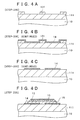
- FIGS. 4 and 5 are schematic sectional views of the support etc.
- the first step is to perform treatment with a silane coupling agent on the surface of the substrate.
- a silane coupling agent On the surface of the substrate, which has been treated with a silane coupling agent, are formed the source/drain electrodes.
- the resist layer 131 is formed by lithography on the insulating layer 111 of SiO 2 as the substrate in the same way as in Step 120 of Example 1.
- the resist layer 131 is patterned such that the part where the source/drain electrodes 14 are to be formed is removed. See FIG. 4A. Incidentally, it is desirable to carry out ashing with oxygen plasma to remove residues of the resist layer 131 after the resist layer 131 has been formed.
- a semiconductor layer is formed on the source/drain electrodes 14 and on that part of the substrate (insulating layer 111) which is held between the source/drain electrodes 14. In this way there is obtained the channel-forming region 15 composed of semiconductor layer on that part of the substrate (insulating layer 111) which is held between the source/drain electrodes 14.
- the same organic semiconductor layer as used in Example 1 is formed by vacuum deposition on the source/drain electrodes 14 and the insulating layer 111 in the same way as in Step 130 in Example 1.
- the gate insulating film 13 is formed on the semiconductor layer.
- the gate insulating film 13 of SiO 2 is formed by sputtering over the entire surface in the same way as in Step 110 in Example 1.
- the gate insulating film 13 is formed on the gate electrode 12.
- a resist layer (not shown) is formed on the gate insulating film 13 (corresponding to the substrate) and the resist layer is patterned by the lithography technology such that the part on which the gate electrode 12 (corresponding to the wiring) is to be formed is removed, in the same way as in Step 100 in Example 1.
- Treatment with a silane coupling agent is performed on the exposed surface of the substrate (the gate insulating film 13) in the same way as in Step 100 in Example 1.
- a metal single-layer film of gold (Au) is formed by vacuum deposition on the resist layer and the substrate (the gate insulating film 13).
- the gate electrode 12 which is composed of a metal single-layer film of gold (Au).
- the resist layer is removed by the lift-off method, such that the wiring (the gate electrode 12) of a metal single-layer film remains on the substrate (the gate insulating film 13). In this way, it is possible to form the gate electrode 12 corresponding to the wiring on the gate insulating film 13 as the substrate. See FIG. 4D.
- Steps 200 to 230 mentioned above achieve the method for producing field effect transistors pertaining to the fifth embodiment of the present invention and the method for forming a metal single-layer film pertaining to the present invention. Also, Step 230 achieve the method for forming wiring pertaining to the second embodiment of the present invention and the method for forming a metal single-layer film pertaining to the first embodiment of the present invention.
- the inter-layer insulating layer 20 of SiO 2 is formed over the entire surface in the same way as in Step 140 in Example 1.
- An opening is formed in that part of the inter-layer insulating layer 20 which is above the word wire (extending from the gate electrode 12) and the source/drain electrodes 14.
- Treatment with a silane coupling agent is performed on the surface of the inter-layer insulating layer 20 (corresponding to the substrate) in the same way as in Step 100 in Example 1.
- a metal single-layer film is formed on the surface of the substrate which has been treated with a silane coupling agent.
- a metal single-layer film of gold (Au) is formed by vacuum deposition on the inter-layer insulating layer 20 including that part within the opening.
- the metal single-layer film is selectively removed (or patterned) by etching. In this way it is possible to form wiring (not shown) connected to the word line extending from the gate electrode 12 and the wiring 21 connected to the source/drain electrode 14 on the inter-layer insulating layer 20 as the substrate. See FIG. 5. In this way there is obtained the desired TFT in Example 2. The TFT showed no sign of peeling in the source/drain electrodes 14, the gate electrode 12, and the wiring 21.
- Step 240 achieves the method for forming wiring pertaining to the third embodiment of the present invention and the method for forming a metal single-layer film pertaining to the first embodiment of the present invention.
- the gate electrode may be formed by the method for forming wiring pertaining to the third embodiment of the present invention, or the wiring 21 on the inter-layer insulating layer 20 may be formed by the method for forming wiring pertaining to the second embodiment of the present invention.
- the structure of the wiring obtained by the method for forming wiring according to the present invention is not limited to the structure of the wiring explained in Examples.
- the field effect transistor (TFT) obtained in the present invention may be made into a monolithic integrated circuit consisting of a large number of TFT's on the support or supporting member. Alternatively, TFT's may be cut into individual pieces for use as discrete parts.
Landscapes
- Engineering & Computer Science (AREA)
- Manufacturing & Machinery (AREA)
- Thin Film Transistor (AREA)
- Electrodes Of Semiconductors (AREA)
- Electroluminescent Light Sources (AREA)
- Internal Circuitry In Semiconductor Integrated Circuit Devices (AREA)
Applications Claiming Priority (2)
| Application Number | Priority Date | Filing Date | Title |
|---|---|---|---|
| JP2003319557A JP2005086147A (ja) | 2003-09-11 | 2003-09-11 | 金属単層膜形成方法、配線形成方法、及び、電界効果型トランジスタの製造方法 |
| JP2003319557 | 2003-09-11 |
Publications (2)
| Publication Number | Publication Date |
|---|---|
| EP1515378A2 true EP1515378A2 (de) | 2005-03-16 |
| EP1515378A3 EP1515378A3 (de) | 2008-04-23 |
Family
ID=34132024
Family Applications (1)
| Application Number | Title | Priority Date | Filing Date |
|---|---|---|---|
| EP04020804A Withdrawn EP1515378A3 (de) | 2003-09-11 | 2004-09-01 | Methode zur Herstellung von Elektroden für Feldteffekttransistoren |
Country Status (6)
| Country | Link |
|---|---|
| US (1) | US7186634B2 (de) |
| EP (1) | EP1515378A3 (de) |
| JP (1) | JP2005086147A (de) |
| KR (1) | KR101164614B1 (de) |
| CN (1) | CN1324656C (de) |
| TW (1) | TWI252525B (de) |
Cited By (5)
| Publication number | Priority date | Publication date | Assignee | Title |
|---|---|---|---|---|
| EP1866981A1 (de) * | 2005-04-05 | 2007-12-19 | Plastic Logic Limited | Strukturierung von metallschichten |
| DE102010044350A1 (de) * | 2010-09-03 | 2012-03-08 | Fraunhofer-Gesellschaft zur Förderung der angewandten Forschung e.V. | Verfahren zur Herstellung einer Metallstruktur auf einer Oberfläche eines Halbleitersubstrates |
| FR2965749A1 (fr) * | 2010-10-12 | 2012-04-13 | Univ Troyes Technologie | Structure multicouche comprenant un métal précieux accroche sur un substrat diélectrique procédé et utilisation associes |
| EP2113944A4 (de) * | 2007-02-23 | 2012-08-22 | Konica Minolta Holdings Inc | Organischer dünnfilmtransistor und verfahren zur herstellung eines organischen dünnfilmtransistors |
| WO2024193157A1 (zh) * | 2023-03-21 | 2024-09-26 | 泉州师范学院 | 一种大面积图案化锡金属栅线电极的常温制备方法 |
Families Citing this family (43)
| Publication number | Priority date | Publication date | Assignee | Title |
|---|---|---|---|---|
| JP4415653B2 (ja) * | 2003-11-19 | 2010-02-17 | セイコーエプソン株式会社 | 薄膜トランジスタの製造方法 |
| JP2006002243A (ja) * | 2004-06-21 | 2006-01-05 | Seiko Epson Corp | マスク、マスクの製造方法、成膜方法、電子デバイス、及び電子機器 |
| KR101058458B1 (ko) * | 2004-09-22 | 2011-08-24 | 엘지디스플레이 주식회사 | 저분자 유기 반도체물질을 이용한 액정표시장치용 어레이기판 및 그의 제조 방법 |
| US7582534B2 (en) * | 2004-11-18 | 2009-09-01 | International Business Machines Corporation | Chemical doping of nano-components |
| TWI292076B (en) * | 2004-12-24 | 2008-01-01 | Au Optronics Corp | Pixel structure and thin film transistor and fabricating methods thereof |
| US7282735B2 (en) * | 2005-03-31 | 2007-10-16 | Xerox Corporation | TFT having a fluorocarbon-containing layer |
| JP2007096129A (ja) * | 2005-09-29 | 2007-04-12 | Kyoto Univ | 分子トランジスタおよびその製造方法、並びにそれを用いた不揮発性メモリおよび圧電センサ |
| JP2007115986A (ja) * | 2005-10-21 | 2007-05-10 | Sharp Corp | 薄膜デバイス及びその製造方法 |
| KR100766318B1 (ko) | 2005-11-29 | 2007-10-11 | 엘지.필립스 엘시디 주식회사 | 유기 반도체 물질을 이용한 박막트랜지스터와 이를 구비한액정표시장치용 어레이 기판 및 그 제조방법 |
| KR101139052B1 (ko) * | 2005-12-06 | 2012-04-30 | 삼성전자주식회사 | 불소를 포함하는 유기절연체 조성물 및 이를 이용한 유기박막 트랜지스터 |
| KR101235135B1 (ko) * | 2005-12-19 | 2013-02-20 | 삼성디스플레이 주식회사 | 금속 배선, 이의 제조 방법, 이를 구비한 표시 기판 및표시 기판의 제조 방법 |
| GB0601008D0 (en) * | 2006-01-18 | 2006-03-01 | Qinetiq Ltd | Method of fabricating a semicondutor device |
| TW200731589A (en) * | 2006-02-06 | 2007-08-16 | Yang Jae Woo | Organic thin film transistor using ultra-thin metal oxide as gate dielectric and fabrication method thereof |
| KR100788758B1 (ko) * | 2006-02-06 | 2007-12-26 | 양재우 | 저전압 유기 박막 트랜지스터 및 그 제조 방법 |
| JP4733005B2 (ja) * | 2006-04-20 | 2011-07-27 | エルジー ディスプレイ カンパニー リミテッド | 有機半導体物質を利用した液晶表示装置用アレイ基板及びその製造方法 |
| KR101163576B1 (ko) | 2006-04-20 | 2012-07-06 | 엘지디스플레이 주식회사 | 유기 반도체물질을 이용한 액정표시장치용 어레이 기판 및그 제조 방법 |
| KR101198219B1 (ko) | 2006-06-23 | 2012-11-07 | 엘지디스플레이 주식회사 | 액정표시장치용 어레이 기판 및 그 제조방법 |
| US8796125B2 (en) * | 2006-06-12 | 2014-08-05 | Kovio, Inc. | Printed, self-aligned, top gate thin film transistor |
| US9196641B2 (en) | 2006-08-15 | 2015-11-24 | Thin Film Electronics Asa | Printed dopant layers |
| US7767520B2 (en) * | 2006-08-15 | 2010-08-03 | Kovio, Inc. | Printed dopant layers |
| JP4293467B2 (ja) * | 2006-09-28 | 2009-07-08 | 国立大学法人京都大学 | 有機材料装置の製造方法 |
| KR101169395B1 (ko) * | 2006-10-13 | 2012-07-30 | 삼성전자주식회사 | 상변화층의 표면처리공정을 포함하는 상변화 메모리 소자의제조방법 |
| KR101274695B1 (ko) * | 2006-11-30 | 2013-06-12 | 엘지디스플레이 주식회사 | 박막트랜지스터 어레이 기판 |
| KR101353824B1 (ko) * | 2007-06-12 | 2014-01-21 | 삼성전자주식회사 | 유기 절연체 형성용 조성물 및 이를 이용하여 제조된 유기절연체 |
| JP2009021309A (ja) * | 2007-07-10 | 2009-01-29 | Ricoh Co Ltd | 電子素子及びその製造方法、並びに該電子素子を備えた表示装置 |
| JP2009021477A (ja) | 2007-07-13 | 2009-01-29 | Sony Corp | 半導体装置およびその製造方法、ならびに表示装置およびその製造方法 |
| US20090104566A1 (en) * | 2007-10-19 | 2009-04-23 | International Business Machines Corporation | Process of multiple exposures with spin castable film |
| TW200920687A (en) * | 2007-11-02 | 2009-05-16 | Delta Electronics Inc | Method for treating surface of element |
| GB0724774D0 (en) * | 2007-12-19 | 2008-01-30 | Cambridge Display Tech Ltd | Organic thin film transistors, active matrix organic optical devices and methods of making the same |
| EP2086033A1 (de) * | 2008-01-31 | 2009-08-05 | Applied Materials, Inc. | Verfahren zur Beschichtung eines Substrats und Beschichtungsanlage |
| DE102011114865B4 (de) | 2011-07-29 | 2023-03-02 | OSRAM Opto Semiconductors Gesellschaft mit beschränkter Haftung | Optoelektronisches Bauelement und Verfahren zur Herstellung eines optoelektronischen Bauelements |
| FR2980041B1 (fr) * | 2011-09-14 | 2016-02-05 | Commissariat Energie Atomique | Transistor a effet de champ comprenant un limiteur de courant de fuite |
| JP2013115098A (ja) * | 2011-11-25 | 2013-06-10 | Sony Corp | トランジスタ、トランジスタの製造方法、表示装置および電子機器 |
| JP6197306B2 (ja) * | 2013-02-22 | 2017-09-20 | 凸版印刷株式会社 | 薄膜トランジスタの製造方法 |
| CN103325732B (zh) * | 2013-06-28 | 2016-03-30 | 京东方科技集团股份有限公司 | 一种coa基板及其制造方法、显示装置 |
| CN103606634B (zh) * | 2013-11-14 | 2016-02-10 | 中国科学院化学研究所 | 一种图案化金属电极及其制备方法 |
| CN105706220B (zh) | 2013-11-21 | 2018-09-18 | 株式会社尼康 | 晶体管的制造方法和晶体管 |
| JP6145032B2 (ja) * | 2013-11-26 | 2017-06-07 | 東京エレクトロン株式会社 | 有機単分子膜の形成方法および形成装置 |
| JP6263450B2 (ja) | 2014-07-24 | 2018-01-17 | 東京エレクトロン株式会社 | 有機単分子膜形成方法 |
| CN105118835A (zh) * | 2015-07-22 | 2015-12-02 | 京东方科技集团股份有限公司 | 阵列基板及其制作方法、显示面板和显示装置 |
| CN107275380B (zh) * | 2017-06-14 | 2020-05-22 | 厦门市三安集成电路有限公司 | 一种化合物半导体的金属层及其制备方法 |
| TWI699892B (zh) * | 2018-09-21 | 2020-07-21 | 友達光電股份有限公司 | 電子裝置及其製造方法 |
| JP2025074478A (ja) * | 2023-10-30 | 2025-05-14 | 日新電機株式会社 | 薄膜トランジスタの製造方法、薄膜トランジスタ |
Citations (3)
| Publication number | Priority date | Publication date | Assignee | Title |
|---|---|---|---|---|
| US5017975A (en) | 1988-07-15 | 1991-05-21 | Matsushita Electric Industrial Co., Ltd. | Organic electronic device with a monomolecular layer or multi-monomolecular layer having electroconductive conjugated bonds |
| WO2001047045A1 (en) | 1999-12-21 | 2001-06-28 | Plastic Logic Limited | Solution processing |
| WO2002095805A2 (en) | 2001-05-23 | 2002-11-28 | Plastic Logic Limited | Laser parrering of devices |
Family Cites Families (18)
| Publication number | Priority date | Publication date | Assignee | Title |
|---|---|---|---|---|
| US4218532A (en) * | 1977-10-13 | 1980-08-19 | Bell Telephone Laboratories, Incorporated | Photolithographic technique for depositing thin films |
| US4204009A (en) * | 1977-12-30 | 1980-05-20 | International Business Machines Corporation | Two layer resist system |
| US4917471A (en) * | 1986-08-30 | 1990-04-17 | Canon Kabushiki Kaisha | Liquid crystal device |
| EP0865078A1 (de) * | 1997-03-13 | 1998-09-16 | Hitachi Europe Limited | Verfahren zum Ablegen von nanometrischen Partikeln |
| TW464980B (en) * | 1999-07-09 | 2001-11-21 | Toshiba Corp | Method for selectively forming copper film |
| JP3646784B2 (ja) * | 2000-03-31 | 2005-05-11 | セイコーエプソン株式会社 | 薄膜パタ−ンの製造方法および微細構造体 |
| KR100462712B1 (ko) * | 2000-08-10 | 2004-12-20 | 마쯔시다덴기산교 가부시키가이샤 | 유기전자장치와 그 제조방법과 그 동작방법 및 그것을 사용한 표시장치 |
| JP2002129329A (ja) * | 2000-10-25 | 2002-05-09 | Sony Corp | タングステン膜の成膜方法 |
| JP3654354B2 (ja) * | 2001-05-28 | 2005-06-02 | 学校法人早稲田大学 | 超lsi配線板及びその製造方法 |
| JP2003051463A (ja) * | 2001-05-29 | 2003-02-21 | Sharp Corp | 金属配線の製造方法およびその方法を用いた金属配線基板 |
| KR100442413B1 (ko) * | 2001-08-04 | 2004-07-30 | 학교법인 포항공과대학교 | 표면에 금속 미세 패턴을 가진 플라스틱 기판의 제조방법 |
| US20030047796A1 (en) * | 2001-09-13 | 2003-03-13 | Zhenan Bao | Narrow channel field effect transistor and method of making the same |
| US6767828B2 (en) * | 2001-10-05 | 2004-07-27 | International Business Machines Corporation | Method for forming patterns for semiconductor devices |
| KR100415617B1 (ko) * | 2001-12-06 | 2004-01-24 | 엘지.필립스 엘시디 주식회사 | 에천트와 이를 이용한 금속배선 제조방법 및박막트랜지스터의 제조방법 |
| JP4259024B2 (ja) * | 2002-02-07 | 2009-04-30 | 富士通株式会社 | 多層配線基板の製造方法およびこれにより製造される多層配線基板 |
| US6740900B2 (en) * | 2002-02-27 | 2004-05-25 | Konica Corporation | Organic thin-film transistor and manufacturing method for the same |
| US20030227014A1 (en) * | 2002-06-11 | 2003-12-11 | Xerox Corporation. | Process for forming semiconductor layer of micro-and nano-electronic devices |
| CN1186822C (zh) * | 2002-09-23 | 2005-01-26 | 中国科学院长春应用化学研究所 | 有机薄膜晶体管及制备方法 |
-
2003
- 2003-09-11 JP JP2003319557A patent/JP2005086147A/ja active Pending
-
2004
- 2004-08-20 US US10/923,372 patent/US7186634B2/en not_active Expired - Fee Related
- 2004-08-30 KR KR1020040068380A patent/KR101164614B1/ko not_active Expired - Fee Related
- 2004-09-01 EP EP04020804A patent/EP1515378A3/de not_active Withdrawn
- 2004-09-10 TW TW093127364A patent/TWI252525B/zh not_active IP Right Cessation
- 2004-09-13 CN CNB2004100752391A patent/CN1324656C/zh not_active Expired - Fee Related
Patent Citations (3)
| Publication number | Priority date | Publication date | Assignee | Title |
|---|---|---|---|---|
| US5017975A (en) | 1988-07-15 | 1991-05-21 | Matsushita Electric Industrial Co., Ltd. | Organic electronic device with a monomolecular layer or multi-monomolecular layer having electroconductive conjugated bonds |
| WO2001047045A1 (en) | 1999-12-21 | 2001-06-28 | Plastic Logic Limited | Solution processing |
| WO2002095805A2 (en) | 2001-05-23 | 2002-11-28 | Plastic Logic Limited | Laser parrering of devices |
Non-Patent Citations (1)
| Title |
|---|
| DORON A. ET AL., LANGMUIR, vol. 11, 1995, pages 1313 - 1317 |
Cited By (7)
| Publication number | Priority date | Publication date | Assignee | Title |
|---|---|---|---|---|
| EP1866981A1 (de) * | 2005-04-05 | 2007-12-19 | Plastic Logic Limited | Strukturierung von metallschichten |
| US7629261B2 (en) | 2005-04-05 | 2009-12-08 | Plastic Logic Limited | Patterning metal layers |
| EP2113944A4 (de) * | 2007-02-23 | 2012-08-22 | Konica Minolta Holdings Inc | Organischer dünnfilmtransistor und verfahren zur herstellung eines organischen dünnfilmtransistors |
| DE102010044350A1 (de) * | 2010-09-03 | 2012-03-08 | Fraunhofer-Gesellschaft zur Förderung der angewandten Forschung e.V. | Verfahren zur Herstellung einer Metallstruktur auf einer Oberfläche eines Halbleitersubstrates |
| FR2965749A1 (fr) * | 2010-10-12 | 2012-04-13 | Univ Troyes Technologie | Structure multicouche comprenant un métal précieux accroche sur un substrat diélectrique procédé et utilisation associes |
| EP2442142A1 (de) * | 2010-10-12 | 2012-04-18 | Université de Technologie de Troyes | Mehrlagige Struktur, die ein auf ein dielektrisches Substrat aufgebrachtes Edelmetall enthält, sowie zugehöriges Verfahren und Verwendung |
| WO2024193157A1 (zh) * | 2023-03-21 | 2024-09-26 | 泉州师范学院 | 一种大面积图案化锡金属栅线电极的常温制备方法 |
Also Published As
| Publication number | Publication date |
|---|---|
| TW200524012A (en) | 2005-07-16 |
| CN1595614A (zh) | 2005-03-16 |
| US7186634B2 (en) | 2007-03-06 |
| KR101164614B1 (ko) | 2012-07-11 |
| JP2005086147A (ja) | 2005-03-31 |
| EP1515378A3 (de) | 2008-04-23 |
| TWI252525B (en) | 2006-04-01 |
| KR20050027006A (ko) | 2005-03-17 |
| CN1324656C (zh) | 2007-07-04 |
| US20050059193A1 (en) | 2005-03-17 |
Similar Documents
| Publication | Publication Date | Title |
|---|---|---|
| US7186634B2 (en) | Method for forming metal single-layer film, method for forming wiring, and method for producing field effect transistors | |
| JP5109223B2 (ja) | 電界効果型トランジスタ | |
| KR101508780B1 (ko) | 유기 박막 트랜지스터의 제조방법 및 그에 의해 제조된 유기 박막 트랜지스터 | |
| US20100219402A1 (en) | Thin film transistor and method for producing the same | |
| US20060027805A1 (en) | Thin film transistor and method of fabricating the same | |
| JP4547864B2 (ja) | 電界効果型トランジスタ及びその製造方法 | |
| JP4569207B2 (ja) | 電界効果型トランジスタの製造方法 | |
| JP4826074B2 (ja) | 電界効果型トランジスタ | |
| JP4710224B2 (ja) | 電界効果型トランジスタ及びその製造方法 | |
| JP5325465B2 (ja) | 薄膜トランジスタおよびそれを用いた装置 | |
| JP5132053B2 (ja) | 有機薄膜トランジスタの製造方法 | |
| JP2007005698A (ja) | 絶縁層及び有機半導体層から成る積層構造の形成方法、並びに、有機電界効果型トランジスタ及びその製造方法 | |
| JP4892810B2 (ja) | 電界効果型トランジスタ | |
| CN100547824C (zh) | 有机绝缘体、包含它的有机薄膜晶体管阵列面板及其制法 | |
| EP2248199A1 (de) | Verfahren zur herstellung von organischen top-gate-halbleitertransistoren | |
| EP2157629A2 (de) | Vorrichtung und Verfahren, die einen Nadelstichbereich umfassen | |
| US20100320463A1 (en) | Method of Fabricating a Semiconductor Device | |
| JP5158010B2 (ja) | 電界効果型トランジスタの製造方法 | |
| JP5110143B2 (ja) | 電界効果型トランジスタ | |
| US20060102954A1 (en) | Organic thin film transistor array panel and manufacturing method thereof | |
| KR101272331B1 (ko) | 유기 박막 트랜지스터 표시판 및 그의 제조 방법 | |
| Zschieschang et al. | Organic thin film transistors with printed gate electrodes | |
| JP2007066925A (ja) | 半導体装置 | |
| WO2010075234A2 (en) | Method of patterning conductive layer and devices made thereby |
Legal Events
| Date | Code | Title | Description |
|---|---|---|---|
| PUAI | Public reference made under article 153(3) epc to a published international application that has entered the european phase |
Free format text: ORIGINAL CODE: 0009012 |
|
| AK | Designated contracting states |
Kind code of ref document: A2 Designated state(s): AT BE BG CH CY CZ DE DK EE ES FI FR GB GR HU IE IT LI LU MC NL PL PT RO SE SI SK TR |
|
| AX | Request for extension of the european patent |
Extension state: AL HR LT LV MK |
|
| PUAL | Search report despatched |
Free format text: ORIGINAL CODE: 0009013 |
|
| AK | Designated contracting states |
Kind code of ref document: A3 Designated state(s): AT BE BG CH CY CZ DE DK EE ES FI FR GB GR HU IE IT LI LU MC NL PL PT RO SE SI SK TR |
|
| AX | Request for extension of the european patent |
Extension state: AL HR LT LV MK |
|
| 17P | Request for examination filed |
Effective date: 20081006 |
|
| AKX | Designation fees paid |
Designated state(s): DE FR GB |
|
| 17Q | First examination report despatched |
Effective date: 20090424 |
|
| STAA | Information on the status of an ep patent application or granted ep patent |
Free format text: STATUS: THE APPLICATION IS DEEMED TO BE WITHDRAWN |
|
| 18D | Application deemed to be withdrawn |
Effective date: 20101123 |