EP1454362B1 - Organischer feld-effekt-transistor mit verschobener schwellwertspannung und verwendung dazu - Google Patents
Organischer feld-effekt-transistor mit verschobener schwellwertspannung und verwendung dazu Download PDFInfo
- Publication number
- EP1454362B1 EP1454362B1 EP02805263A EP02805263A EP1454362B1 EP 1454362 B1 EP1454362 B1 EP 1454362B1 EP 02805263 A EP02805263 A EP 02805263A EP 02805263 A EP02805263 A EP 02805263A EP 1454362 B1 EP1454362 B1 EP 1454362B1
- Authority
- EP
- European Patent Office
- Prior art keywords
- ofet
- layer
- threshold voltage
- interlayer
- gate
- Prior art date
- Legal status (The legal status is an assumption and is not a legal conclusion. Google has not performed a legal analysis and makes no representation as to the accuracy of the status listed.)
- Expired - Lifetime
Links
- 230000005669 field effect Effects 0.000 title description 3
- 239000010410 layer Substances 0.000 claims description 29
- 239000004065 semiconductor Substances 0.000 claims description 12
- 239000012212 insulator Substances 0.000 claims description 8
- 239000011229 interlayer Substances 0.000 claims description 7
- XMWRBQBLMFGWIX-UHFFFAOYSA-N C60 fullerene Chemical class C12=C3C(C4=C56)=C7C8=C5C5=C9C%10=C6C6=C4C1=C1C4=C6C6=C%10C%10=C9C9=C%11C5=C8C5=C8C7=C3C3=C7C2=C1C1=C2C4=C6C4=C%10C6=C9C9=C%11C5=C5C8=C3C3=C7C1=C1C2=C4C6=C2C9=C5C3=C12 XMWRBQBLMFGWIX-UHFFFAOYSA-N 0.000 claims description 2
- 229910003472 fullerene Inorganic materials 0.000 claims description 2
- 150000002979 perylenes Chemical class 0.000 claims description 2
- 150000004756 silanes Chemical class 0.000 claims description 2
- 239000011529 conductive interlayer Substances 0.000 claims 1
- 239000000463 material Substances 0.000 claims 1
- 239000002800 charge carrier Substances 0.000 description 5
- 238000004519 manufacturing process Methods 0.000 description 5
- 238000004770 highest occupied molecular orbital Methods 0.000 description 3
- 238000004768 lowest unoccupied molecular orbital Methods 0.000 description 3
- 229910004298 SiO 2 Inorganic materials 0.000 description 2
- XUIMIQQOPSSXEZ-UHFFFAOYSA-N Silicon Chemical compound [Si] XUIMIQQOPSSXEZ-UHFFFAOYSA-N 0.000 description 2
- 238000009825 accumulation Methods 0.000 description 2
- QVGXLLKOCUKJST-UHFFFAOYSA-N atomic oxygen Chemical compound [O] QVGXLLKOCUKJST-UHFFFAOYSA-N 0.000 description 2
- 230000015572 biosynthetic process Effects 0.000 description 2
- 238000010276 construction Methods 0.000 description 2
- 230000007717 exclusion Effects 0.000 description 2
- 239000011368 organic material Substances 0.000 description 2
- 229910052760 oxygen Inorganic materials 0.000 description 2
- 239000001301 oxygen Substances 0.000 description 2
- 239000000758 substrate Substances 0.000 description 2
- PYJJCSYBSYXGQQ-UHFFFAOYSA-N trichloro(octadecyl)silane Chemical compound CCCCCCCCCCCCCCCCCC[Si](Cl)(Cl)Cl PYJJCSYBSYXGQQ-UHFFFAOYSA-N 0.000 description 2
- 239000004020 conductor Substances 0.000 description 1
- 238000000151 deposition Methods 0.000 description 1
- 239000003989 dielectric material Substances 0.000 description 1
- 238000007598 dipping method Methods 0.000 description 1
- 229910052751 metal Inorganic materials 0.000 description 1
- 239000002184 metal Substances 0.000 description 1
- 229910044991 metal oxide Inorganic materials 0.000 description 1
- 150000002739 metals Chemical class 0.000 description 1
- 238000000034 method Methods 0.000 description 1
- SLIUAWYAILUBJU-UHFFFAOYSA-N pentacene Chemical compound C1=CC=CC2=CC3=CC4=CC5=CC=CC=C5C=C4C=C3C=C21 SLIUAWYAILUBJU-UHFFFAOYSA-N 0.000 description 1
- 239000002985 plastic film Substances 0.000 description 1
- 229920006255 plastic film Polymers 0.000 description 1
- 229920000642 polymer Polymers 0.000 description 1
- 238000007639 printing Methods 0.000 description 1
- 229910052710 silicon Inorganic materials 0.000 description 1
- 239000010703 silicon Substances 0.000 description 1
- 238000004528 spin coating Methods 0.000 description 1
- 238000010025 steaming Methods 0.000 description 1
- 239000010409 thin film Substances 0.000 description 1
Images

Classifications
-
- H—ELECTRICITY
- H10—SEMICONDUCTOR DEVICES; ELECTRIC SOLID-STATE DEVICES NOT OTHERWISE PROVIDED FOR
- H10K—ORGANIC ELECTRIC SOLID-STATE DEVICES
- H10K10/00—Organic devices specially adapted for rectifying, amplifying, oscillating or switching; Organic capacitors or resistors having potential barriers
- H10K10/40—Organic transistors
- H10K10/46—Field-effect transistors, e.g. organic thin-film transistors [OTFT]
- H10K10/462—Insulated gate field-effect transistors [IGFETs]
- H10K10/464—Lateral top-gate IGFETs comprising only a single gate
Definitions
- a key parameter in organic field effect transistors is the location of the threshold voltage. This voltage indicates at which gate voltage the current channel of the transistor arises or becomes conductive. If this is close to 0 V, two problems arise in the construction of integrated circuits from these OFETs: two instead of just one voltage supply is required, and about twice the number of transistors is required, since the output voltages of the logic elements must be shifted before adding more Logic elements can be controlled. Result of these problems is u.a. a greatly increased power consumption, which makes it difficult to use polymer electronics, in other words electronics based on organic materials, in applications such as RF-ID tags (Radio Frequency Identification).
- RF-ID tags Radio Frequency Identification
- an OFET is known, which is manufactured as follows: From a gate electrode, a silicon substrate layer is applied to which a thermally grown SiO 2 layer is applied. Prior to depositing the organic semiconductor layer, the surface of the SiO 2 layer is pretreated by vapor deposited octadecyltrichlorosilane (OTS) monolayers. Subsequently, the organic semiconductor layer is evaporated on the pretreated surface.
- OTS octadecyltrichlorosilane
- the object of the invention is therefore to provide a possibility for shifting the threshold voltage in OFETs, in particular those whose threshold voltage is close to 0V or in the positive range available.
- the invention is an OFET according to claim 1.
- the interlayer creates a space charge zone that prevents the formation of a conductive current channel at low gate voltages. Only for larger gate voltages does the normal generation of a current channel take place. Thus, the threshold voltage is shifted, without the disadvantages such as reduction of the ON / OFF ratio, etc. or lower output currents must be accepted. Whether the threshold voltage shift is 2V, 5V, or over 10V depends on the thickness and donor concentration of the interlayer, and can be adjusted as appropriate by appropriate choice. This represents an important advantage of the disclosure of the invention.
- a further advantage of the invention is that OFETs with this intermediate layer are significantly less sensitive to inadvertent background doping of the semiconductor, since it is actively compensated by the intermediate layer. This facilitates the production of OFETs, since then e.g. can be dispensed with production under exclusion of oxygen.
- the intermediate layer is comprised of small, polarizable molecules with internal dipole moment (e.g., di-sulfide dipole molecules) or silanes, fullerenes, or perylenes.
- the interlayer is a few to several tens of nanometers thick.
- the intermediate layer is applied to the semiconductor layer (top-gate OFETs).
- This application may be by spin-coating, pouring, printing, steaming, dipping in solution, or other application method.
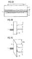
- FIG. 1a shows a cross section through a conventional OFET with a substrate 8 (eg a plastic film), the structured source / drain electrodes 7, the organic semiconductor layer 6, the insulator layer 2 and the gate electrode 1.
- FIG. 1b shows the corresponding position of the LUMO or HOMO energies for the layer sequence gate electrode / insulator / semiconductor: LUMO energy 3 (corresponds to the energetic position of the conduction band), HOMO energy 5 (corresponds to the energetic position of the valence band) and the Fermi level 4.
- An increase of the gate voltage by ⁇ U 1 leads to an accumulation of the charge carriers at the interface between insulator and semiconductor (9 in Figure 1c ). This leads to an increase in the energy levels in the organic semiconductor layer 6 near the interface. The increase in the gate voltage thus leads directly to the formation of a current channel 9 in the OFET.
- FIG. 2a shows the construction of an OFET according to an embodiment of the invention.
- the space charge generating layer 10 Between the insulator layer 2 and: the semiconductive layer 6 is the space charge generating layer 10. Main characteristics of this layer are a low work function, as well as a high number of donors. Due to these properties, the charge carriers of the adjacent semiconductor layer are bound to these donors. This creates a space charge zone. ie an area where there are no free charge carriers. In the FIG. 2b One recognizes this space charge zone through the downwardly bent LUMO and HOMO levels 3 and 4 near the semiconductor / insulator interface. If the gate voltage is increased at this OFET, no current channel can be generated at low voltages since all donors must first be filled with holes.
- Contents of the invention is the introduction of a very thin, non-conductive layer between semiconducting material and insulator in OFET.
- the invention makes it possible for the first time to shift the threshold voltage of an OFET and at the same time to simplify the production of the OFET, since it is possible to dispense with oxygen exclusion during production.
Landscapes
- Thin Film Transistor (AREA)
Description
- Ein Schlüsselparameter bei organischen Feldeffekt-Transistoren (OFETs) ist die Lage der Schwellwertspannung. Diese Spannung gibt an, bei welcher Gate-Spannung der Stromkanal des Transistors entsteht oder leitfähig wird. Liegt diese nahe bei 0V, so treten beim Aufbau von integrierten Schaltungen aus diesen OFETs zwei Problemen auf: es werden zwei statt nur einer Spannungsversorgung benötigt und man braucht etwa die doppelte Anzahl von Transistoren, da die Ausgangsspannungen der Logikelemente verschoben werden müssen, bevor damit weitere Logikelemente angesteuert werden können. Folge dieser Probleme ist u.a. ein stark erhöhter Leistungsverbrauch, der gerade bei Anwendungen wie RF-ID-Tags (Radio-Frequency-Identification) einen Einsatz von Polymerelektronik, also Elektronik auf Basis organischer Materialien erschwert.
- Bei den für zukünftige Anwendungen aussichtsreichsten OFETs, den auf Polyalkylthiophen basierenden, wie sie z.B. aus der Veröffentlichung von H. Sirringhaus (H. Sirringhaus, N. Tessler, et al. (1999). Elsevier Synthetic Metals 102: 857-860) bekannt sind, liegt die Schwellwertspannung nahe bei 0V. Bei OFETs mit Pentacene als Halbeleiter liegt die Schwellwertspannung sogar bei positiven Spannungen (C.D. Sheraw, J.A. Nichols et al. (2000), IEDM 2000, p.619-22). Es treten daher die oben beschriebenen Probleme auf. Da OFETs auf dem Prinzip der Ladungsträgerakkumulation basieren, lässt sich die Lage der Schwellwertspannung nicht, wie z.B. bei Si-MOS-FETs (Silizium-Metall-Oxid Feldeffekt-Transistoren) üblich, durch die Kanaldicke einstellen. Auch eine dickere Isolatorschicht verschiebt die Schwellwertspannung nur unwesentlich. Dadurch würde gleichzeitig das on/off-Verhältnis des OFETs deutlich verschlechtert. Die naheliegende Möglichkeit zur Verschiebung der Schwellwertspannung, nämlich eine Gate-Elektrode zu verwenden, welche eine niedrigere Austrittsarbeit hat, ist keine brauchbare Lösung, da sich solche aus leitfähigem organischen Material praktisch nicht realisieren lassen.
- Aus der SPIE Vol 4466 (2001), Artikel "Improved Organic Thin Film Transistor Performance Using Chemically-Modified Gate Dielectrics" Gundlach D.J. et al, Seite 54 bis 64, 29.07.2001 ist weiter ein OFET bekannt, der wie folgt gefertigt wird: Aus eine Gate-Elektrode wird eine Silizium-Substratschicht aufgebracht auf der eine Thermisch gewachsene SiO2-Schicht aufgebracht wird. Vor Abscheiden der organischen Halbleiterschicht wird die Oberfläche der SiO2-Schicht durch aus der Gasphase abgeschiedene Octadecyltrichlorosilan (OTS)-Monoschichten Vorbehandelt. Anschließend wird die organische Halbleiterschicht auf die vorbehandelte Oberfläche aufgedampft.
- Aufgabe der Erfindung ist es daher, eine Möglichkeit zur Verschiebung der Schwellwertspannung bei OFETs, insbesondere bei solchen, deren Schwellwertspannung nahe 0V oder im positiven Bereich liegt, zur Verfügung zu stellen. Außerdem ist es Aufgabe der Erfindung, Verwendungen von OFETs mit verschobener Schwellwertspannung zu offenbaren.
- Gegenstand der Erfindung ist ein OFET nach Anspruch 1.
- Als wird ein Bereich bezeichnet, in dem sich keine freien Ladungsträger befinden.
- Die Zwischenschicht erzeugt eine Raumladungszone, die die Ausbildung eines leitfähigen Stromkanals bei kleinen Gate-Spannungen verhindert. Erst für größere Gate-Spannungen findet die normale Erzeugung eines Stromkanals statt. Damit wird die Schwellwertspannung verschoben, ohne dass die Nachteile wie Verringerung des ON/OFF-Verhältnisses etc. oder niedrigere Ausgangsströme in Kauf genommen werden müssen. Ob die Verschiebung der Schwellwertspannung 2V, 5V oder über 10V beträgt, hängt von der Dicke und der Donatorkonzentration der Zwischenschicht ab und kann durch geeignete Wahl je nach Bedarf eingestellt werden. Dies stellt einen wichtigen Vorteil der Erfindungsmeldung dar.
- Ein weiterer Vorteil der Erfindung ist, dass OFETs mit dieser Zwischenschicht deutlich unempfindlicher gegenüber einer unabsichtlichen Hintergrunddotierung des Halbleiters sind, da diese aktiv durch die Zwischenschicht kompensiert wird. Das erleichtert die Herstellung von OFETs, da dann z.B. auf eine Herstellung unter Sauerstoffausschluss verzichtet werden kann.
- Nach einer Ausführungsform ist die Zwischenschicht aus kleinen, polarisierbaren Molekülen mit internen Dipolmoment (z.B. Di-Sulfid-Dipolmoleküle) oder aus Silanen, Fullerenen oder Perylenen.
- Nach einer Ausführungsform ist die Zwischenschicht einige wenige bis einige 10 Nanometer dick.
- Bei der Herstellung organischer Transistoren oder organischer integrierter Schaltungen wird die Zwischenschicht auf die Halbleiterschicht (Top-Gate OFETs) aufgebracht. Dieses Aufbringen kann durch Aufschleudern, Aufgießen, Drucken, Bedampfen, Eintauchen in eine Lösung oder durch eine andere Aufbringungsmethode geschehen.
- Die nachfolgende Erläuterung erfolgt anhand von Figuren die Ausführungsbeispiele der Erfindung mit p-leitende OFETs zeigen
-
Figuren 1a bis 1c zeigen den Stand der Technik zum Vergleich; -
Figuren 2a bis 2c zeigen dieselben Ansichten bei einem Ausführungsbeispiel der Erfindung. -
Figur 1a zeigt einen Querschnitt durch einen herkömmlichen OFET mit einem Substrat 8 (z.B. einer Plastikfolie), den strukturierten Source/Drain-Elektroden 7, der organischen Halbleiterschicht 6, der Isolatorschicht 2 und der Gate-Elektrode 1.Figur 1b zeigt die dazugehörige Lage der LUMO- bzw. HOMO- Energien für die Schichtabfolge Gate-Elektrode /Isolator / Halbleiter: LUMO-Energie 3 (entspricht der energetischen Lage des Leitungsbandes), HOMO-Energie 5 (entspricht der energetischen Lage des Valenzbandes) und das Fermi-Niveau 4. Eine Erhöhung der Gate-Spannung um ΔU1 führt zu einer Akkumulation der Ladungsträger an der Grenzfläche zwischen Isolator und Halbleiter (9 inFigur 1c ). Dies führt zu einer Anhebung der Energieniveaus in der organischen Halbleiterschicht 6 nahe der Grenzfläche. Die Erhöhung der Gate-Spannung führt also direkt zur Ausbildung eines Stromkanals 9 im OFET. -
Figur 2a zeigt den Aufbau eines OFETs gemäß einer Ausführungsform der Erfindung. Zwischen der Isolatorschicht 2 und: der halbleitenden Schicht 6 befindet sich die raumladungserzeugende Schicht 10. Haupteigenschaften dieser Schicht sind eine geringe Austrittsarbeit, sowie eine hohe Zahl von Donatoren. Aufgrund dieser Eigenschaften werden die Ladungsträger der angrenzenden Halbleiterschicht an diese Donatoren gebunden. Dadurch entsteht eine Raumladungszone. d.h. ein Bereich, indem sich keine freien Ladungsträger befinden. In derFigur 2b erkennt man diese Raumladungszone durch die nach unten verbogenen LUMO- und HOMO-Niveaus 3 und 4 nahe der Grenzfläche Halbleiter / Isolator. Erhöht man an diesen OFET die Gate-Spannung, so kann bei kleinen Spannungen noch kein Stromkanal erzeugt werden, da zuerst alle Donatoren mit Löchern gefüllt werden müssen. Erst bei einer höheren Spannung ΔU2, wenn die Donatoren kompensiert sind, kann ein Stromkanal 9 im OFET erzeugt werden (sieheFigur 2c ). Die Differenz zischen der Spannung ΔU1 (inFig. 1c ) und ΔU2 (inFig. 2c ) entspricht der Verschiebung der Schwellwertspannung. - Inhalt der Erfindung ist die Einführung einer sehr dünnen, nichtleitenden Schicht zwischen halbleitendem Material und Isolator im OFET. Durch die Erfindung wird es erstmals möglich, die Schwellwertspannung eines OFETs zu verschieben und gleichzeitig die Herstellung des OFETs zu vereinfachen, da auf Sauerstoffaussschluß während der Herstellung verzichtet werden kann.
Claims (5)
- OFET, zwischen zwei Elektrodenschichten, einer
Source/DrainElektrodenschicht und einer Gate-Elektrodenschicht zumindest eine aktive Schicht umfassend, wobei zwischen der Gate-Isolatorschicht und der aktiven, p-halbleitenden Schicht eine nichtleitende zwischen 1 und 50 Nanometer dicke Zwischenschicht angeordnet ist, die aus einem
Material mit einer Anzahl an Donatoren ausgebildet ist, die so gewählt ist, dass sich durch die Donatoren eine Raumladungszone in der aktiven Schicht ausbildet und sich die Schwellwertspannung des OFET dadurch verschiebt,
dadurch gekennzeichnet, dass die Zwischenschicht auf die aktive p-halbleitende Schicht aufgebracht ist und dass der OFET ein Top-Gate OFET ist. - OFET nach Anspruch 1, bei dem die Zwischenschicht aus kleinen, polarisierbaren Molekülen mit internem Dipolmoment besteht.
- OFET nach einem der vorstehenden Ansprüche, dessen halbleitendes Material Polyalkylthiophen ist.
- OFET nach einem der Ansprüche 1 oder 3, bei dem die Zwischenschicht aus Di-Sulfid-Dipolmolekülen oder aus Silanen, Fullerenen oder Perylenen ist.
- Verwendung eines OFET nach einem der vorstehenden Ansprüche 1 bis 4 in einem RFID Tag.
Applications Claiming Priority (3)
| Application Number | Priority Date | Filing Date | Title |
|---|---|---|---|
| DE10160732 | 2001-12-11 | ||
| DE10160732A DE10160732A1 (de) | 2001-12-11 | 2001-12-11 | Organischer Feld-Effekt-Transistor mit verschobener Schwellwertspannung und Verwendung dazu |
| PCT/DE2002/004520 WO2003054970A1 (de) | 2001-12-11 | 2002-12-09 | Organischer feld-effekt-transistor mit verschobener schwellwertspannung und verwendung dazu |
Publications (2)
| Publication Number | Publication Date |
|---|---|
| EP1454362A1 EP1454362A1 (de) | 2004-09-08 |
| EP1454362B1 true EP1454362B1 (de) | 2010-03-31 |
Family
ID=7708749
Family Applications (1)
| Application Number | Title | Priority Date | Filing Date |
|---|---|---|---|
| EP02805263A Expired - Lifetime EP1454362B1 (de) | 2001-12-11 | 2002-12-09 | Organischer feld-effekt-transistor mit verschobener schwellwertspannung und verwendung dazu |
Country Status (5)
| Country | Link |
|---|---|
| US (1) | US7064345B2 (de) |
| EP (1) | EP1454362B1 (de) |
| JP (1) | JP2005513802A (de) |
| DE (2) | DE10160732A1 (de) |
| WO (1) | WO2003054970A1 (de) |
Families Citing this family (22)
| Publication number | Priority date | Publication date | Assignee | Title |
|---|---|---|---|---|
| DE10043204A1 (de) * | 2000-09-01 | 2002-04-04 | Siemens Ag | Organischer Feld-Effekt-Transistor, Verfahren zur Strukturierung eines OFETs und integrierte Schaltung |
| JP4254123B2 (ja) * | 2002-04-08 | 2009-04-15 | コニカミノルタホールディングス株式会社 | 有機薄膜トランジスタおよびその製造方法 |
| JP2004165427A (ja) * | 2002-11-13 | 2004-06-10 | Konica Minolta Holdings Inc | 有機薄膜トランジスタ素子 |
| JP4228204B2 (ja) * | 2003-07-07 | 2009-02-25 | セイコーエプソン株式会社 | 有機トランジスタの製造方法 |
| DE10340608A1 (de) | 2003-08-29 | 2005-03-24 | Infineon Technologies Ag | Polymerformulierung und Verfahren zur Herstellung einer Dielektrikumsschicht |
| DE10349029B4 (de) * | 2003-11-07 | 2006-09-28 | Polyic Gmbh & Co. Kg | Verwendung von Poly(alkoxythiophen) als Funktionsschicht in elektrischen Bauelementen |
| JP4850389B2 (ja) * | 2003-12-12 | 2012-01-11 | 独立行政法人産業技術総合研究所 | ドーピング方法およびそれを用いた半導体素子 |
| JP4661065B2 (ja) * | 2004-03-22 | 2011-03-30 | セイコーエプソン株式会社 | 相補型有機半導体装置 |
| JP2006090983A (ja) * | 2004-09-27 | 2006-04-06 | Univ Of Tokyo | 面状素子モジュールおよびその製造方法並びに面状素子装置 |
| JP4883898B2 (ja) * | 2004-11-18 | 2012-02-22 | パナソニック株式会社 | 電子デバイスおよびそれを用いた電子機器 |
| KR100637204B1 (ko) | 2005-01-15 | 2006-10-23 | 삼성에스디아이 주식회사 | 박막 트랜지스터, 그 제조 방법 및 이를 구비한 평판 표시장치 |
| DE102005017655B4 (de) * | 2005-04-15 | 2008-12-11 | Polyic Gmbh & Co. Kg | Mehrschichtiger Verbundkörper mit elektronischer Funktion |
| WO2006134942A1 (ja) * | 2005-06-14 | 2006-12-21 | Mitsumi Electric Co., Ltd. | 電界効果トランジスタ、それを具備するバイオセンサ、および検出方法 |
| DE102005031448A1 (de) | 2005-07-04 | 2007-01-11 | Polyic Gmbh & Co. Kg | Aktivierbare optische Schicht |
| DE102005035590A1 (de) * | 2005-07-29 | 2007-02-01 | Polyic Gmbh & Co. Kg | Elektronisches Bauelement |
| DE102005035589A1 (de) | 2005-07-29 | 2007-02-01 | Polyic Gmbh & Co. Kg | Verfahren zur Herstellung eines elektronischen Bauelements |
| US7935957B2 (en) * | 2005-08-12 | 2011-05-03 | Semiconductor Energy Laboratory Co., Ltd. | Memory device and a semiconductor device |
| DE102005042166A1 (de) * | 2005-09-06 | 2007-03-15 | Polyic Gmbh & Co.Kg | Organisches Bauelement und ein solches umfassende elektrische Schaltung |
| DE102005044306A1 (de) * | 2005-09-16 | 2007-03-22 | Polyic Gmbh & Co. Kg | Elektronische Schaltung und Verfahren zur Herstellung einer solchen |
| ITMI20051901A1 (it) * | 2005-10-10 | 2007-04-11 | St Microelectronics Srl | Processo di fabbricazione di tramsistori a film sottile in materiale organico e transistore |
| DE102007000875A1 (de) | 2007-11-12 | 2009-05-14 | Bundesdruckerei Gmbh | Dokument mit einer integrierten Anzeigevorrichtung |
| TWI618232B (zh) | 2013-09-09 | 2018-03-11 | 應用材料股份有限公司 | 工程誘發的可調靜電效應 |
Citations (2)
| Publication number | Priority date | Publication date | Assignee | Title |
|---|---|---|---|---|
| EP0786820A2 (de) * | 1996-01-29 | 1997-07-30 | Motorola, Inc. | Organischer Dünnfilmtransistor mit verbesserter Ladungsträgerbeweglichkeit |
| WO2004114371A2 (de) * | 2003-06-20 | 2004-12-29 | Infineon Technologies Ag | Verbindung zur bildung einer selbstorganisierenden monolage, schichtstruktur, halbleiterbauelement mit einer schichtstruktur und verfahren zur herstellung einer schichtstruktur |
Family Cites Families (189)
| Publication number | Priority date | Publication date | Assignee | Title |
|---|---|---|---|---|
| GB723598A (en) | 1951-09-07 | 1955-02-09 | Philips Nv | Improvements in or relating to methods of producing electrically conductive mouldings from plastics |
| US3512052A (en) | 1968-01-11 | 1970-05-12 | Gen Motors Corp | Metal-insulator-semiconductor voltage variable capacitor with controlled resistivity dielectric |
| US3769096A (en) | 1971-03-12 | 1973-10-30 | Bell Telephone Labor Inc | Pyroelectric devices |
| JPS543594B2 (de) | 1973-10-12 | 1979-02-24 | ||
| JPS5638918Y2 (de) | 1977-10-25 | 1981-09-10 | ||
| JPS54101176A (en) | 1978-01-26 | 1979-08-09 | Shinetsu Polymer Co | Contact member for push switch |
| US4442019A (en) | 1978-05-26 | 1984-04-10 | Marks Alvin M | Electroordered dipole suspension |
| JPS5641938U (de) | 1979-09-10 | 1981-04-17 | ||
| US4340657A (en) | 1980-02-19 | 1982-07-20 | Polychrome Corporation | Novel radiation-sensitive articles |
| JPS59145576A (ja) | 1982-11-09 | 1984-08-21 | ザイトレツクス・コ−ポレ−シヨン | プログラム可能なmosトランジスタ |
| DE3321071A1 (de) | 1983-06-10 | 1984-12-13 | Basf Ag | Druckschalter |
| DE3338597A1 (de) | 1983-10-24 | 1985-05-02 | GAO Gesellschaft für Automation und Organisation mbH, 8000 München | Datentraeger mit integriertem schaltkreis und verfahren zur herstellung desselben |
| JPS60117769A (ja) | 1983-11-30 | 1985-06-25 | Fujitsu Ltd | 半導体メモリ装置 |
| JPS61167854U (de) | 1985-04-10 | 1986-10-17 | ||
| DE3751376T2 (de) | 1986-10-13 | 1995-11-16 | Canon Kk | Schaltungselement. |
| JP2728412B2 (ja) | 1987-12-25 | 1998-03-18 | 株式会社日立製作所 | 半導体装置 |
| GB2215307B (en) | 1988-03-04 | 1991-10-09 | Unisys Corp | Electronic component transportation container |
| ATE100616T1 (de) | 1988-06-21 | 1994-02-15 | Gec Avery Ltd | Herstellung von tragbaren elektronischen karten. |
| US5364735A (en) | 1988-07-01 | 1994-11-15 | Sony Corporation | Multiple layer optical record medium with protective layers and method for producing same |
| US4937119A (en) | 1988-12-15 | 1990-06-26 | Hoechst Celanese Corp. | Textured organic optical data storage media and methods of preparation |
| US5892244A (en) | 1989-01-10 | 1999-04-06 | Mitsubishi Denki Kabushiki Kaisha | Field effect transistor including πconjugate polymer and liquid crystal display including the field effect transistor |
| US6331356B1 (en) | 1989-05-26 | 2001-12-18 | International Business Machines Corporation | Patterns of electrically conducting polymers and their application as electrodes or electrical contacts |
| DE69018348T2 (de) | 1989-07-25 | 1995-08-03 | Matsushita Electric Ind Co Ltd | Speicherbauelement aus organischem Halbleiter mit einer MISFET-Struktur und sein Kontrollverfahren. |
| US5206525A (en) | 1989-12-27 | 1993-04-27 | Nippon Petrochemicals Co., Ltd. | Electric element capable of controlling the electric conductivity of π-conjugated macromolecular materials |
| FI91573C (sv) | 1990-01-04 | 1994-07-11 | Neste Oy | Sätt att framställa elektroniska och elektro-optiska komponenter och kretsar |
| FR2664430B1 (fr) | 1990-07-04 | 1992-09-18 | Centre Nat Rech Scient | Transistor a effet de champ en couche mince de structure mis, dont l'isolant et le semiconducteur sont realises en materiaux organiques. |
| US5376561A (en) | 1990-12-31 | 1994-12-27 | Kopin Corporation | High density electronic circuit modules |
| FR2673041A1 (fr) | 1991-02-19 | 1992-08-21 | Gemplus Card Int | Procede de fabrication de micromodules de circuit integre et micromodule correspondant. |
| EP0501456A3 (de) | 1991-02-26 | 1992-09-09 | Sony Corporation | Mit eine optischen Plattenantrieb ausgerüsteter Videospielcomputer |
| US5408109A (en) | 1991-02-27 | 1995-04-18 | The Regents Of The University Of California | Visible light emitting diodes fabricated from soluble semiconducting polymers |
| JP3522771B2 (ja) | 1991-03-22 | 2004-04-26 | 三菱電機株式会社 | インバータ |
| US5332315A (en) | 1991-04-27 | 1994-07-26 | Gec Avery Limited | Apparatus and sensor unit for monitoring changes in a physical quantity with time |
| JP3224829B2 (ja) | 1991-08-15 | 2001-11-05 | 株式会社東芝 | 有機電界効果型素子 |
| JPH0580530A (ja) | 1991-09-24 | 1993-04-02 | Hitachi Ltd | 薄膜パターン製造方法 |
| US5173835A (en) | 1991-10-15 | 1992-12-22 | Motorola, Inc. | Voltage variable capacitor |
| DE59105477D1 (de) | 1991-10-30 | 1995-06-14 | Fraunhofer Ges Forschung | Belichtungsvorrichtung. |
| JP2709223B2 (ja) | 1992-01-30 | 1998-02-04 | 三菱電機株式会社 | 非接触形携帯記憶装置 |
| JP3150750B2 (ja) | 1992-03-13 | 2001-03-26 | 日本写真印刷株式会社 | 有機整流素子 |
| JPH05347422A (ja) | 1992-06-16 | 1993-12-27 | Fujitsu Ltd | 二安定ダイオード |
| DE4243832A1 (de) | 1992-12-23 | 1994-06-30 | Daimler Benz Ag | Tastsensoranordnung |
| JP3457348B2 (ja) | 1993-01-15 | 2003-10-14 | 株式会社東芝 | 半導体装置の製造方法 |
| WO1994017556A1 (en) | 1993-01-26 | 1994-08-04 | Fci-Fiberchem, Inc. | Optical sensor with electroluminescent light source and polymer light detector |
| FR2701117B1 (fr) | 1993-02-04 | 1995-03-10 | Asulab Sa | Système de mesures électrochimiques à capteur multizones, et son application au dosage du glucose. |
| US5567550A (en) | 1993-03-25 | 1996-10-22 | Texas Instruments Incorporated | Method of making a mask for making integrated circuits |
| JPH0722669A (ja) | 1993-07-01 | 1995-01-24 | Mitsubishi Electric Corp | 可塑性機能素子 |
| JP3035352B2 (ja) | 1993-08-24 | 2000-04-24 | メトリカ・インコーポレーテッド | 新規な使い捨て電子検定ディバイス |
| JP3460863B2 (ja) | 1993-09-17 | 2003-10-27 | 三菱電機株式会社 | 半導体装置の製造方法 |
| FR2710413B1 (fr) | 1993-09-21 | 1995-11-03 | Asulab Sa | Dispositif de mesure pour capteurs amovibles. |
| US5556706A (en) | 1993-10-06 | 1996-09-17 | Matsushita Electric Industrial Co., Ltd. | Conductive layered product and method of manufacturing the same |
| IL111151A (en) | 1994-10-03 | 1998-09-24 | News Datacom Ltd | Secure access systems |
| WO1995031831A1 (en) | 1994-05-18 | 1995-11-23 | Philips Electronics N.V. | Method of providing a film of conjugated, substituted or unsubstituted poly(p-phenylene vinylene) on a substrate by chemical vapour deposition (cvd), as well as a method of manufacturing an electroluminescent (el) device |
| US5684884A (en) | 1994-05-31 | 1997-11-04 | Hitachi Metals, Ltd. | Piezoelectric loudspeaker and a method for manufacturing the same |
| JP3246189B2 (ja) | 1994-06-28 | 2002-01-15 | 株式会社日立製作所 | 半導体表示装置 |
| ATE227881T1 (de) | 1994-07-14 | 2002-11-15 | Surgx Corp | Verfahren zur herstellung von ein- und mehrschicht-schutzvorrichtungen gegen veränderliche spannung |
| US5574291A (en) | 1994-12-09 | 1996-11-12 | Lucent Technologies Inc. | Article comprising a thin film transistor with low conductivity organic layer |
| US5630986A (en) | 1995-01-13 | 1997-05-20 | Bayer Corporation | Dispensing instrument for fluid monitoring sensors |
| JPH08197788A (ja) | 1995-01-27 | 1996-08-06 | Hitachi Koki Co Ltd | プリンタ制御装置の画像データ読出し回路 |
| JP3068430B2 (ja) | 1995-04-25 | 2000-07-24 | 富山日本電気株式会社 | 固体電解コンデンサ及びその製造方法 |
| US5652645A (en) | 1995-07-24 | 1997-07-29 | Anvik Corporation | High-throughput, high-resolution, projection patterning system for large, flexible, roll-fed, electronic-module substrates |
| GB9519698D0 (en) | 1995-09-27 | 1995-11-29 | Rivaz Antony C De | Educational toys and games |
| WO1997018944A1 (en) | 1995-11-22 | 1997-05-29 | The Government Of The United States Of America, Represented By The Secretary Of The Navy | Patterned conducting polymer surfaces and process for preparing the same and devices containing the same |
| US5625199A (en) | 1996-01-16 | 1997-04-29 | Lucent Technologies Inc. | Article comprising complementary circuit with inorganic n-channel and organic p-channel thin film transistors |
| GB2310493B (en) | 1996-02-26 | 2000-08-02 | Unilever Plc | Determination of the characteristics of fluid |
| JP3080579B2 (ja) | 1996-03-06 | 2000-08-28 | 富士機工電子株式会社 | エアリア・グリッド・アレイ・パッケージの製造方法 |
| DE19629656A1 (de) | 1996-07-23 | 1998-01-29 | Boehringer Mannheim Gmbh | Diagnostischer Testträger mit mehrschichtigem Testfeld und Verfahren zur Bestimmung von Analyt mit dessen Hilfe |
| AUPO307296A0 (en) | 1996-10-18 | 1996-11-14 | Erico Lightning Technologies Pty Ltd | An improved lightning conductor |
| DE19644254A1 (de) | 1996-10-24 | 1998-05-07 | Steag Micro Tech Gmbh | Vorrichtung zum Behandeln von Substraten |
| WO1998040930A1 (en) | 1997-03-10 | 1998-09-17 | Precision Dynamics Corporation | Reactively coupled elements in circuits on flexible substrates |
| US6344662B1 (en) | 1997-03-25 | 2002-02-05 | International Business Machines Corporation | Thin-film field-effect transistor with organic-inorganic hybrid semiconductor requiring low operating voltages |
| KR100248392B1 (ko) | 1997-05-15 | 2000-09-01 | 정선종 | 유기물전계효과트랜지스터와결합된유기물능동구동전기발광소자및그소자의제작방법 |
| GB9715907D0 (en) | 1997-07-29 | 1997-10-01 | Cambridge Consultants | Electroluminescent device production process |
| EP0968537B1 (de) | 1997-08-22 | 2012-05-02 | Creator Technology B.V. | Feld-effekt-transistor, der im wesentlichen aus organischen materialien besteht |
| WO1999010929A2 (en) | 1997-08-22 | 1999-03-04 | Koninklijke Philips Electronics N.V. | A method of providing a vertical interconnect between thin film microelectronic devices |
| AU764920B2 (en) | 1997-09-11 | 2003-09-04 | Precision Dynamics Corporation | Radio frequency identification tag on flexible substrate |
| WO1999021233A1 (en) | 1997-10-17 | 1999-04-29 | The Regents Of The University Of California | Process for fabricating organic semiconductor devices using ink-jet printing technology and device and system employing same |
| US6251513B1 (en) | 1997-11-08 | 2001-06-26 | Littlefuse, Inc. | Polymer composites for overvoltage protection |
| JPH11142810A (ja) | 1997-11-12 | 1999-05-28 | Nintendo Co Ltd | 携帯型情報処理装置 |
| JP2001510670A (ja) | 1997-12-05 | 2001-07-31 | コーニンクレッカ フィリップス エレクトロニクス エヌ ヴィ | 識別トランスポンダ |
| US5997817A (en) | 1997-12-05 | 1999-12-07 | Roche Diagnostics Corporation | Electrochemical biosensor test strip |
| US5998805A (en) | 1997-12-11 | 1999-12-07 | Motorola, Inc. | Active matrix OED array with improved OED cathode |
| US6083104A (en) | 1998-01-16 | 2000-07-04 | Silverlit Toys (U.S.A.), Inc. | Programmable toy with an independent game cartridge |
| NO306529B1 (no) | 1998-01-16 | 1999-11-15 | Opticom As | Transistor |
| AU739848B2 (en) | 1998-01-28 | 2001-10-18 | Thin Film Electronics Asa | A method for generation of electrical conducting or semiconducting structures in three dimensions and methods for erasure of the same structures |
| US6087196A (en) | 1998-01-30 | 2000-07-11 | The Trustees Of Princeton University | Fabrication of organic semiconductor devices using ink jet printing |
| US6045977A (en) | 1998-02-19 | 2000-04-04 | Lucent Technologies Inc. | Process for patterning conductive polyaniline films |
| DE19816860A1 (de) | 1998-03-06 | 1999-11-18 | Deutsche Telekom Ag | Chipkarte, insbesondere Guthabenkarte |
| US6033202A (en) | 1998-03-27 | 2000-03-07 | Lucent Technologies Inc. | Mold for non - photolithographic fabrication of microstructures |
| GB9808061D0 (en) | 1998-04-16 | 1998-06-17 | Cambridge Display Tech Ltd | Polymer devices |
| GB9808806D0 (en) | 1998-04-24 | 1998-06-24 | Cambridge Display Tech Ltd | Selective deposition of polymer films |
| TW410478B (en) | 1998-05-29 | 2000-11-01 | Lucent Technologies Inc | Thin-film transistor monolithically integrated with an organic light-emitting diode |
| US5967048A (en) | 1998-06-12 | 1999-10-19 | Howard A. Fromson | Method and apparatus for the multiple imaging of a continuous web |
| KR100282393B1 (ko) | 1998-06-17 | 2001-02-15 | 구자홍 | 유기이엘(el)디스플레이소자제조방법 |
| US6528816B1 (en) | 1998-06-19 | 2003-03-04 | Thomas Jackson | Integrated inorganic/organic complementary thin-film transistor circuit and a method for its production |
| DE19836174C2 (de) | 1998-08-10 | 2000-10-12 | Illig Maschinenbau Adolf | Heizung zum Erwärmen von thermoplastischen Kunststoffplatten und Verfahren zum Einstellen der Temperatur dieser Heizung |
| US6215130B1 (en) | 1998-08-20 | 2001-04-10 | Lucent Technologies Inc. | Thin film transistors |
| JP4689825B2 (ja) | 1998-08-26 | 2011-05-25 | センサーズ・フォー・メデセン・アンド・サイエンス・インコーポレーテッド | 光学式検知装置 |
| JP4493741B2 (ja) | 1998-09-04 | 2010-06-30 | 株式会社半導体エネルギー研究所 | 半導体装置の作製方法 |
| DE19851703A1 (de) | 1998-10-30 | 2000-05-04 | Inst Halbleiterphysik Gmbh | Verfahren zur Herstellung von elektronischen Strukturen |
| US6384804B1 (en) | 1998-11-25 | 2002-05-07 | Lucent Techonologies Inc. | Display comprising organic smart pixels |
| GB9825992D0 (en) | 1998-11-28 | 1999-01-20 | Moorlodge Biotech Ventures Lim | Electrochemical sensor |
| US6506438B2 (en) | 1998-12-15 | 2003-01-14 | E Ink Corporation | Method for printing of transistor arrays on plastic substrates |
| US6321571B1 (en) | 1998-12-21 | 2001-11-27 | Corning Incorporated | Method of making glass structures for flat panel displays |
| US6114088A (en) | 1999-01-15 | 2000-09-05 | 3M Innovative Properties Company | Thermal transfer element for forming multilayer devices |
| GB2347013A (en) | 1999-02-16 | 2000-08-23 | Sharp Kk | Charge-transport structures |
| US6300141B1 (en) | 1999-03-02 | 2001-10-09 | Helix Biopharma Corporation | Card-based biosensor device |
| US6180956B1 (en) | 1999-03-03 | 2001-01-30 | International Business Machine Corp. | Thin film transistors with organic-inorganic hybrid materials as semiconducting channels |
| US6207472B1 (en) | 1999-03-09 | 2001-03-27 | International Business Machines Corporation | Low temperature thin film transistor fabrication |
| US6498114B1 (en) | 1999-04-09 | 2002-12-24 | E Ink Corporation | Method for forming a patterned semiconductor film |
| US6072716A (en) | 1999-04-14 | 2000-06-06 | Massachusetts Institute Of Technology | Memory structures and methods of making same |
| FR2793089B3 (fr) | 1999-04-28 | 2001-06-08 | Rene Liger | Transpondeur a antenne integree |
| DE19919448A1 (de) | 1999-04-29 | 2000-11-02 | Miele & Cie | Kühlgerät und Verfahren zur Verkeimungsindikation |
| DE19921024C2 (de) | 1999-05-06 | 2001-03-08 | Wolfgang Eichelmann | Videospielanlage |
| EP1052594A1 (de) | 1999-05-14 | 2000-11-15 | Sokymat S.A. | Transponder und Spritzgussteil sowie Verfahren zu ihrer Herstellung |
| CA2374236C (en) | 1999-06-21 | 2014-12-23 | Cambridge University Technical Services Limited | Aligned polymers for an organic tft |
| TW556357B (en) | 1999-06-28 | 2003-10-01 | Semiconductor Energy Lab | Method of manufacturing an electro-optical device |
| CA2377671C (en) | 1999-07-01 | 2011-01-04 | David F. Bocian | High density non-volatile memory device |
| JP2001085272A (ja) | 1999-07-14 | 2001-03-30 | Matsushita Electric Ind Co Ltd | 可変容量コンデンサ |
| DE19933757A1 (de) | 1999-07-19 | 2001-01-25 | Giesecke & Devrient Gmbh | Chipkarte mit integrierter Batterie |
| AU6174700A (en) | 1999-07-20 | 2001-02-05 | Alvin Wai Lun Yip | Carrier tray for integrated circuits such as microprocessors |
| ATE549753T1 (de) | 1999-07-21 | 2012-03-15 | E Ink Corp | Reaktive herstellung von dielektrischen schichten und schutz von organischen schichten in organischen halbleiteranordnungen |
| DE19935527A1 (de) | 1999-07-28 | 2001-02-08 | Giesecke & Devrient Gmbh | Aktive Folie für Chipkarten mit Display |
| DE19937262A1 (de) | 1999-08-06 | 2001-03-01 | Siemens Ag | Anordnung mit Transistor-Funktion |
| CN1183595C (zh) | 1999-08-24 | 2005-01-05 | 皇家菲利浦电子有限公司 | 显示装置 |
| JP4972260B2 (ja) | 1999-08-31 | 2012-07-11 | イー インク コーポレイション | パターニングされた半導体膜を形成する方法 |
| US6545291B1 (en) | 1999-08-31 | 2003-04-08 | E Ink Corporation | Transistor design for use in the construction of an electronically driven display |
| US6593690B1 (en) | 1999-09-03 | 2003-07-15 | 3M Innovative Properties Company | Large area organic electronic devices having conducting polymer buffer layers and methods of making same |
| US6517995B1 (en) | 1999-09-14 | 2003-02-11 | Massachusetts Institute Of Technology | Fabrication of finely featured devices by liquid embossing |
| EP1224999A4 (de) | 1999-09-28 | 2007-05-02 | Sumitomo Heavy Industries | Laserbohrverfahren und laserbohrvorrichtung |
| US6340822B1 (en) | 1999-10-05 | 2002-01-22 | Agere Systems Guardian Corp. | Article comprising vertically nano-interconnected circuit devices and method for making the same |
| JP2004538618A (ja) | 1999-10-11 | 2004-12-24 | コーニンクレッカ フィリップス エレクトロニクス エヌ ヴィ | 集積回路 |
| US6335539B1 (en) | 1999-11-05 | 2002-01-01 | International Business Machines Corporation | Method for improving performance of organic semiconductors in bottom electrode structure |
| US6284562B1 (en) | 1999-11-17 | 2001-09-04 | Agere Systems Guardian Corp. | Thin film transistors |
| EP1103916A1 (de) | 1999-11-24 | 2001-05-30 | Infineon Technologies AG | Chipkarte |
| US6621098B1 (en) | 1999-11-29 | 2003-09-16 | The Penn State Research Foundation | Thin-film transistor and methods of manufacturing and incorporating a semiconducting organic material |
| US6136702A (en) | 1999-11-29 | 2000-10-24 | Lucent Technologies Inc. | Thin film transistors |
| US6197663B1 (en) | 1999-12-07 | 2001-03-06 | Lucent Technologies Inc. | Process for fabricating integrated circuit devices having thin film transistors |
| AU2015901A (en) | 1999-12-21 | 2001-07-03 | Plastic Logic Limited | Inkjet-fabricated integrated circuits |
| AU779878B2 (en) | 1999-12-21 | 2005-02-17 | Flexenable Limited | Forming interconnects |
| CN1245769C (zh) | 1999-12-21 | 2006-03-15 | 造型逻辑有限公司 | 溶液加工 |
| US6706159B2 (en) | 2000-03-02 | 2004-03-16 | Diabetes Diagnostics | Combined lancet and electrochemical analyte-testing apparatus |
| DE10012204A1 (de) | 2000-03-13 | 2001-09-20 | Siemens Ag | Einrichtung zum Kennzeichnen von Stückgut |
| EP1134694A1 (de) | 2000-03-16 | 2001-09-19 | Infineon Technologies AG | Dokument mit integrierter elektronischer Schaltung |
| HK1053151B (en) | 2000-03-28 | 2006-05-26 | Diabetes Diagnostics, Inc. | Continuous process for manufacture of disposable electro-chemical sensor |
| US6441196B2 (en) * | 2000-05-19 | 2002-08-27 | Alcon, Inc. | Processes and novel intermediates for 11-oxa prostaglandin synthesis |
| US6329226B1 (en) | 2000-06-01 | 2001-12-11 | Agere Systems Guardian Corp. | Method for fabricating a thin-film transistor |
| DE10033112C2 (de) | 2000-07-07 | 2002-11-14 | Siemens Ag | Verfahren zur Herstellung und Strukturierung organischer Feldeffekt-Transistoren (OFET), hiernach gefertigter OFET und seine Verwendung |
| US6867539B1 (en) | 2000-07-12 | 2005-03-15 | 3M Innovative Properties Company | Encapsulated organic electronic devices and method for making same |
| WO2002015264A2 (de) | 2000-08-18 | 2002-02-21 | Siemens Aktiengesellschaft | Verkapseltes organisch-elektronisches bauteil, verfahren zu seiner herstellung und seine verwendung |
| DE10120687A1 (de) | 2001-04-27 | 2002-10-31 | Siemens Ag | Verkapseltes organisch-elektronisches Bauteil, Verfahren zu seiner Herstellung und seine Verwendung |
| JP2002068324A (ja) | 2000-08-30 | 2002-03-08 | Nippon Sanso Corp | 断熱容器 |
| DE10043204A1 (de) | 2000-09-01 | 2002-04-04 | Siemens Ag | Organischer Feld-Effekt-Transistor, Verfahren zur Strukturierung eines OFETs und integrierte Schaltung |
| DE10045192A1 (de) | 2000-09-13 | 2002-04-04 | Siemens Ag | Organischer Datenspeicher, RFID-Tag mit organischem Datenspeicher, Verwendung eines organischen Datenspeichers |
| DE10047171A1 (de) | 2000-09-22 | 2002-04-18 | Siemens Ag | Elektrode und/oder Leiterbahn für organische Bauelemente und Herstellungverfahren dazu |
| GB0024294D0 (en) | 2000-10-04 | 2000-11-15 | Univ Cambridge Tech | Solid state embossing of polymer devices |
| KR20020036916A (ko) | 2000-11-11 | 2002-05-17 | 주승기 | 실리콘 박막의 결정화 방법 및 이에 의해 제조된 반도체소자 |
| DE10058559A1 (de) | 2000-11-24 | 2002-05-29 | Interactiva Biotechnologie Gmb | System zur Abwicklung eines Warentransfers und Warenvorrats-Behälter |
| NO20005980L (no) | 2000-11-27 | 2002-05-28 | Thin Film Electronics Ab | Ferroelektrisk minnekrets og fremgangsmåte ved dens fremstilling |
| KR100390522B1 (ko) | 2000-12-01 | 2003-07-07 | 피티플러스(주) | 결정질 실리콘 활성층을 포함하는 박막트랜지스터 제조 방법 |
| DE10061297C2 (de) | 2000-12-08 | 2003-05-28 | Siemens Ag | Verfahren zur Sturkturierung eines OFETs |
| DE10105914C1 (de) | 2001-02-09 | 2002-10-10 | Siemens Ag | Organischer Feldeffekt-Transistor mit fotostrukturiertem Gate-Dielektrikum und ein Verfahren zu dessen Erzeugung |
| EP1237207B1 (de) | 2001-03-02 | 2012-01-04 | FUJIFILM Corporation | Herstellungsverfahren einer organischen Dünnschicht-Vorrichtung |
| WO2002071139A1 (en) | 2001-03-07 | 2002-09-12 | Acreo Ab | Electrochemical pixel device |
| SE520339C2 (sv) | 2001-03-07 | 2003-06-24 | Acreo Ab | Elektrokemisk transistoranordning och dess tillverkningsförfarande |
| KR100861916B1 (ko) | 2001-03-26 | 2008-10-09 | 닛신보세키 가부시키 가이샤 | 이온성 액체, 축전 디바이스용 전해질염, 축전 디바이스용전해액, 전기 2중층 캐패시터, 및 2차전지 |
| US20020167003A1 (en) * | 2001-04-18 | 2002-11-14 | Campbell Ian H. | Chemical and biological sensor using organic self-assembled transitors |
| AU2002340793A1 (en) | 2001-05-07 | 2002-11-18 | Coatue Corporation | Molecular memory device |
| US20020170897A1 (en) | 2001-05-21 | 2002-11-21 | Hall Frank L. | Methods for preparing ball grid array substrates via use of a laser |
| EP1393389B1 (de) | 2001-05-23 | 2018-12-05 | Flexenable Limited | Musterung von anordnungen mittels laser |
| DE10126859A1 (de) | 2001-06-01 | 2002-12-12 | Siemens Ag | Verfahren zur Erzeugung von leitfähigen Strukturen mittels Drucktechnik sowie daraus hergestellte aktive Bauelemente für integrierte Schaltungen |
| DE10126860C2 (de) | 2001-06-01 | 2003-05-28 | Siemens Ag | Organischer Feldeffekt-Transistor, Verfahren zu seiner Herstellung und Verwendung zum Aufbau integrierter Schaltungen |
| US6870180B2 (en) | 2001-06-08 | 2005-03-22 | Lucent Technologies Inc. | Organic polarizable gate transistor apparatus and method |
| JP2003089259A (ja) | 2001-09-18 | 2003-03-25 | Hitachi Ltd | パターン形成方法およびパターン形成装置 |
| US7351660B2 (en) | 2001-09-28 | 2008-04-01 | Hrl Laboratories, Llc | Process for producing high performance interconnects |
| DE10156470B4 (de) | 2001-11-16 | 2006-06-08 | Infineon Technologies Ag | RF-ID-Etikett mit einer Halbleiteranordnung mit Transistoren auf Basis organischer Halbleiter und nichtflüchtiger Schreib-Lese-Speicherzellen |
| JP2003234473A (ja) | 2002-02-06 | 2003-08-22 | Canon Inc | 有機半導体素子の製造方法 |
| FI20020296A7 (fi) | 2002-02-14 | 2003-08-15 | Rafsec Oy | Älytarra |
| US6946332B2 (en) | 2002-03-15 | 2005-09-20 | Lucent Technologies Inc. | Forming nanoscale patterned thin film metal layers |
| DE10212640B4 (de) | 2002-03-21 | 2004-02-05 | Siemens Ag | Logische Bauteile aus organischen Feldeffekttransistoren |
| DE10219905B4 (de) | 2002-05-03 | 2011-06-22 | OSRAM Opto Semiconductors GmbH, 93055 | Optoelektronisches Bauelement mit organischen funktionellen Schichten und zwei Trägern sowie Verfahren zur Herstellung eines solchen optoelektronischen Bauelements |
| EP1362682A1 (de) | 2002-05-13 | 2003-11-19 | ZBD Displays Ltd, | Verfahren und Vorrichtung zum Ausrichten von Flüssigkristallen |
| US6812509B2 (en) | 2002-06-28 | 2004-11-02 | Palo Alto Research Center Inc. | Organic ferroelectric memory cells |
| EP1559147B1 (de) | 2002-10-02 | 2014-11-12 | Leonhard Kurz Stiftung & Co. KG | Folie mit organischen halbleitern |
| US6870183B2 (en) | 2002-11-04 | 2005-03-22 | Advanced Micro Devices, Inc. | Stacked organic memory devices and methods of operating and fabricating |
| EP1559148A2 (de) | 2002-11-05 | 2005-08-03 | Siemens Aktiengesellschaft | ORGANISCHES ELEKTRONISCHES BAUTEIL MIT HOCHAUFGELöSTER STRUKTURIERUNG UND HERSTELLUNGSVERFAHREN DAZU |
| DE50306538D1 (de) | 2002-11-19 | 2007-03-29 | Polyic Gmbh & Co Kg | Organische elektronische schaltung mit stukturierter halbleitender funktionsschicht und herstellungsverfahren dazu |
| WO2004066348A2 (de) * | 2003-01-21 | 2004-08-05 | Polyic Gmbh & Co. Kg | Organisches elektronikbauteil und verfahren zur herstellung organischer elektronik |
| DE10302149A1 (de) * | 2003-01-21 | 2005-08-25 | Siemens Ag | Verwendung leitfähiger Carbon-black/Graphit-Mischungen für die Herstellung von low-cost Elektronik |
| GB0306098D0 (en) | 2003-03-18 | 2003-04-23 | Platform Diagnostics Group Ltd | Sample testing device |
| US7253084B2 (en) * | 2004-09-03 | 2007-08-07 | Asm America, Inc. | Deposition from liquid sources |
-
2001
- 2001-12-11 DE DE10160732A patent/DE10160732A1/de not_active Ceased
-
2002
- 2002-09-12 US US10/498,610 patent/US7064345B2/en not_active Expired - Fee Related
- 2002-12-09 WO PCT/DE2002/004520 patent/WO2003054970A1/de not_active Ceased
- 2002-12-09 EP EP02805263A patent/EP1454362B1/de not_active Expired - Lifetime
- 2002-12-09 JP JP2003555592A patent/JP2005513802A/ja active Pending
- 2002-12-09 DE DE50214320T patent/DE50214320D1/de not_active Expired - Lifetime
Patent Citations (2)
| Publication number | Priority date | Publication date | Assignee | Title |
|---|---|---|---|---|
| EP0786820A2 (de) * | 1996-01-29 | 1997-07-30 | Motorola, Inc. | Organischer Dünnfilmtransistor mit verbesserter Ladungsträgerbeweglichkeit |
| WO2004114371A2 (de) * | 2003-06-20 | 2004-12-29 | Infineon Technologies Ag | Verbindung zur bildung einer selbstorganisierenden monolage, schichtstruktur, halbleiterbauelement mit einer schichtstruktur und verfahren zur herstellung einer schichtstruktur |
Non-Patent Citations (5)
| Title |
|---|
| DODABALAPUR A. ET AL.: "Organic field-effect bipolar transistors", APPLIED PHYSICS LETTERS, vol. 68, no. 8, 19 February 1996 (1996-02-19), pages 1108 - 1110 * |
| DODABALAPUR A; ET AL: "ORGANIC HETEROSTRUCTURE FIELD-EFFECT TRANSISTORS", SCIENCE, vol. 269, 15 September 1995 (1995-09-15), pages 1560 - 1562, XP000644688 * |
| GUNDLACH D. ET AL.: "Improved organic thin film transistor performance using chemically-modified gate dielectrics", PROCEEDINGS OF THE SPIE, vol. 4466, 26 July 2001 (2001-07-26), pages 54 - 64, XP001149892, DOI: doi:10.1117/12.451466 * |
| JACKSON T.N. ET AL.: "Organic thin film transistors for organic light-emitting flat-panel display backplanes", IEEE JOURNAL OF SELECTED TOPICS IN QUANTUM ELECTRONICS, vol. 4, no. 1, January 1998 (1998-01-01) - February 1998 (1998-02-01), pages 100 - 104, XP000766109, DOI: doi:10.1109/2944.669475 * |
| MORITA S; ZAKHIDOV A A; YOSHINO K: "Doping effect of Buckminsterfullerene in conducting polymer: change of absorption spectrum and quenching of luminescence", SOLID STATE COMMUNICATIONS, vol. 82, no. 4, April 1992 (1992-04-01), pages 249 - 252, XP024635014, DOI: doi:10.1016/0038-1098(92)90636-N * |
Also Published As
| Publication number | Publication date |
|---|---|
| US7064345B2 (en) | 2006-06-20 |
| DE10160732A1 (de) | 2003-06-26 |
| WO2003054970A1 (de) | 2003-07-03 |
| US20050211972A1 (en) | 2005-09-29 |
| DE50214320D1 (de) | 2010-05-12 |
| JP2005513802A (ja) | 2005-05-12 |
| EP1454362A1 (de) | 2004-09-08 |
Similar Documents
| Publication | Publication Date | Title |
|---|---|---|
| EP1454362A1 (de) | Organischer feld-effekt-transistor mit verschobener schwellwertspannung und verwendung dazu | |
| Haddon | C70 thin film transistors | |
| Lin et al. | High-performance carbon nanotube field-effect transistor with tunable polarities | |
| Gentili et al. | Logic-gate devices based on printed polymer semiconducting nanostripes | |
| Chen et al. | Low-voltage organic thin-film transistors with polymeric nanocomposite dielectrics | |
| DE112008003142T5 (de) | Organische Dünnfilmtransistoren, organische optische Aktiv-Matrix-Vorrichtungen und Verfahren zur Herstellung derselben | |
| DE112009001881T5 (de) | Verfahren zur Herstellung von organischen Dünnschichttransistoren unter Verwendung eines laserinduzierten thermischen Transferdruckprozesses | |
| DE112009000736T5 (de) | Organische Dünnfilm-Transistoren | |
| DE19937262A1 (de) | Anordnung mit Transistor-Funktion | |
| DE112008003420T5 (de) | Organische Dünnschichttransistoren, organische optische Vorrichtungen mit aktiver Matrix und Verfahren zu ihrer Herstellung | |
| DE602004005824T2 (de) | Elektronische vorrichtung | |
| KR20150043237A (ko) | 유기 전계 효과 트랜지스터 및 이를 제조하기 위한 방법 | |
| WO2007125036A2 (de) | Organo-magnetoresistiver sensor und verwendungen dazu | |
| JP5477750B2 (ja) | 有機電界効果型トランジスタ | |
| WO2001001502A2 (en) | A means for electrical contacting or isolation of organic or inorganic semiconductors and a method for its fabrication | |
| EP1825516A2 (de) | Gatter aus organischen feldeffekttransistoren | |
| DE112010000849T5 (de) | Verfahren zum Bilden von Source- und Drain-Elektoden organischer Dünnfilmtransistoren durch stromloses Plattieren | |
| CN1674320B (zh) | 有机场效应晶体管及制造方法和含该晶体管的平板显示器 | |
| DE10209400A1 (de) | Transponderschaltung mit einer Gleichrichterschaltung sowie Verfahren zur Herstellung einer Transponderschaltung mit einer Gleichrichterschaltung | |
| DE102012112796B4 (de) | Vertikaler organischer Transistor, Schaltungsanordnung und Anordnung mit vertikalem organischen Transistor sowie Verfahren zum Herstellen | |
| WO2008125100A1 (de) | Organisches elektronisches speicherbauelement, speicherbauelementanordnung und verfahren zum betreiben eines organischen elektronischen speicherbauelementes | |
| Jang et al. | Inkjet printed carbon nanotubes in short channel field effect transistors: influence of nanotube distortion and gate insulator interface modification | |
| DE102008036063A1 (de) | Organischer Feldeffekt-Transistor | |
| DE102010031979B4 (de) | Halbleiterbauelement, Verfahren zu dessen Herstellung, Verwendung des Halbleiterbauelementes und Inverter mit zwei Halbleiterbauelementen | |
| Pandey et al. | Performance analysis of dual gate-OTFT with variation in OSC thickness and channel length |
Legal Events
| Date | Code | Title | Description |
|---|---|---|---|
| PUAI | Public reference made under article 153(3) epc to a published international application that has entered the european phase |
Free format text: ORIGINAL CODE: 0009012 |
|
| 17P | Request for examination filed |
Effective date: 20040407 |
|
| AK | Designated contracting states |
Kind code of ref document: A1 Designated state(s): AT BE BG CH CY CZ DE DK EE ES FI FR GB GR IE IT LI LU MC NL PT SE SI SK TR |
|
| AX | Request for extension of the european patent |
Extension state: AL LT LV MK RO |
|
| RIN1 | Information on inventor provided before grant (corrected) |
Inventor name: ULLMANN, ANDREAS Inventor name: FIX, WALTER |
|
| RAP1 | Party data changed (applicant data changed or rights of an application transferred) |
Owner name: POLYIC GMBH & CO. KG |
|
| RAP1 | Party data changed (applicant data changed or rights of an application transferred) |
Owner name: POLYIC GMBH & CO. KG |
|
| 17Q | First examination report despatched |
Effective date: 20070606 |
|
| GRAP | Despatch of communication of intention to grant a patent |
Free format text: ORIGINAL CODE: EPIDOSNIGR1 |
|
| RIC1 | Information provided on ipc code assigned before grant |
Ipc: H01L 51/10 20060101AFI20090904BHEP |
|
| GRAS | Grant fee paid |
Free format text: ORIGINAL CODE: EPIDOSNIGR3 |
|
| RIN1 | Information on inventor provided before grant (corrected) |
Inventor name: ULLMANN, ANDREAS Inventor name: FIX, WALTER |
|
| GRAA | (expected) grant |
Free format text: ORIGINAL CODE: 0009210 |
|
| AK | Designated contracting states |
Kind code of ref document: B1 Designated state(s): DE FR GB |
|
| REG | Reference to a national code |
Ref country code: GB Ref legal event code: FG4D Free format text: NOT ENGLISH |
|
| REF | Corresponds to: |
Ref document number: 50214320 Country of ref document: DE Date of ref document: 20100512 Kind code of ref document: P |
|
| PLBE | No opposition filed within time limit |
Free format text: ORIGINAL CODE: 0009261 |
|
| STAA | Information on the status of an ep patent application or granted ep patent |
Free format text: STATUS: NO OPPOSITION FILED WITHIN TIME LIMIT |
|
| 26N | No opposition filed |
Effective date: 20110104 |
|
| PGFP | Annual fee paid to national office [announced via postgrant information from national office to epo] |
Ref country code: DE Payment date: 20131127 Year of fee payment: 12 Ref country code: GB Payment date: 20131217 Year of fee payment: 12 |
|
| PGFP | Annual fee paid to national office [announced via postgrant information from national office to epo] |
Ref country code: FR Payment date: 20131213 Year of fee payment: 12 |
|
| REG | Reference to a national code |
Ref country code: DE Ref legal event code: R119 Ref document number: 50214320 Country of ref document: DE |
|
| GBPC | Gb: european patent ceased through non-payment of renewal fee |
Effective date: 20141209 |
|
| REG | Reference to a national code |
Ref country code: FR Ref legal event code: ST Effective date: 20150831 |
|
| PG25 | Lapsed in a contracting state [announced via postgrant information from national office to epo] |
Ref country code: DE Free format text: LAPSE BECAUSE OF NON-PAYMENT OF DUE FEES Effective date: 20150701 Ref country code: GB Free format text: LAPSE BECAUSE OF NON-PAYMENT OF DUE FEES Effective date: 20141209 |
|
| PG25 | Lapsed in a contracting state [announced via postgrant information from national office to epo] |
Ref country code: FR Free format text: LAPSE BECAUSE OF NON-PAYMENT OF DUE FEES Effective date: 20141231 |