EP1424735B1 - Method for forming light-absorbing layer - Google Patents
Method for forming light-absorbing layer Download PDFInfo
- Publication number
- EP1424735B1 EP1424735B1 EP02733434A EP02733434A EP1424735B1 EP 1424735 B1 EP1424735 B1 EP 1424735B1 EP 02733434 A EP02733434 A EP 02733434A EP 02733434 A EP02733434 A EP 02733434A EP 1424735 B1 EP1424735 B1 EP 1424735B1
- Authority
- EP
- European Patent Office
- Prior art keywords
- precursor
- thin
- layer
- group metal
- metal
- Prior art date
- Legal status (The legal status is an assumption and is not a legal conclusion. Google has not performed a legal analysis and makes no representation as to the accuracy of the status listed.)
- Expired - Fee Related
Links
- 238000000034 method Methods 0.000 title claims description 35
- 239000010410 layer Substances 0.000 claims description 82
- 229910052751 metal Inorganic materials 0.000 claims description 55
- 239000002243 precursor Substances 0.000 claims description 55
- 239000002184 metal Substances 0.000 claims description 47
- 239000011669 selenium Substances 0.000 claims description 28
- 239000000758 substrate Substances 0.000 claims description 26
- 238000004544 sputter deposition Methods 0.000 claims description 23
- 239000010409 thin film Substances 0.000 claims description 22
- 229910052738 indium Inorganic materials 0.000 claims description 16
- 229910052711 selenium Inorganic materials 0.000 claims description 15
- 239000002245 particle Substances 0.000 claims description 14
- BUGBHKTXTAQXES-UHFFFAOYSA-N Selenium Chemical compound [Se] BUGBHKTXTAQXES-UHFFFAOYSA-N 0.000 claims description 13
- 229910045601 alloy Inorganic materials 0.000 claims description 8
- 239000000956 alloy Substances 0.000 claims description 8
- 229910052733 gallium Inorganic materials 0.000 claims description 8
- 150000002739 metals Chemical class 0.000 claims description 8
- 239000002356 single layer Substances 0.000 claims description 6
- 238000004519 manufacturing process Methods 0.000 claims description 4
- 229910052782 aluminium Inorganic materials 0.000 claims description 2
- 239000010949 copper Substances 0.000 description 16
- 238000006243 chemical reaction Methods 0.000 description 15
- 239000010408 film Substances 0.000 description 13
- 239000007789 gas Substances 0.000 description 12
- 239000005361 soda-lime glass Substances 0.000 description 10
- 150000001875 compounds Chemical class 0.000 description 9
- 229910052802 copper Inorganic materials 0.000 description 9
- 238000010438 heat treatment Methods 0.000 description 9
- 239000004065 semiconductor Substances 0.000 description 8
- 238000005275 alloying Methods 0.000 description 5
- APFVFJFRJDLVQX-UHFFFAOYSA-N indium atom Chemical compound [In] APFVFJFRJDLVQX-UHFFFAOYSA-N 0.000 description 5
- 239000000203 mixture Substances 0.000 description 5
- SPVXKVOXSXTJOY-UHFFFAOYSA-N selane Chemical compound [SeH2] SPVXKVOXSXTJOY-UHFFFAOYSA-N 0.000 description 5
- 229910000058 selane Inorganic materials 0.000 description 5
- XKRFYHLGVUSROY-UHFFFAOYSA-N Argon Chemical compound [Ar] XKRFYHLGVUSROY-UHFFFAOYSA-N 0.000 description 4
- 229910000807 Ga alloy Inorganic materials 0.000 description 4
- 238000007796 conventional method Methods 0.000 description 4
- 239000013078 crystal Substances 0.000 description 4
- 239000000047 product Substances 0.000 description 4
- ZOKXTWBITQBERF-UHFFFAOYSA-N Molybdenum Chemical compound [Mo] ZOKXTWBITQBERF-UHFFFAOYSA-N 0.000 description 3
- 102100022068 Serine palmitoyltransferase 1 Human genes 0.000 description 3
- 101710122478 Serine palmitoyltransferase 1 Proteins 0.000 description 3
- 101710122477 Serine palmitoyltransferase 2 Proteins 0.000 description 3
- 238000001816 cooling Methods 0.000 description 3
- 238000000151 deposition Methods 0.000 description 3
- 229910052750 molybdenum Inorganic materials 0.000 description 3
- 239000011733 molybdenum Substances 0.000 description 3
- 102100027677 Protein SPT2 homolog Human genes 0.000 description 2
- 229910052786 argon Inorganic materials 0.000 description 2
- CDZGJSREWGPJMG-UHFFFAOYSA-N copper gallium Chemical compound [Cu].[Ga] CDZGJSREWGPJMG-UHFFFAOYSA-N 0.000 description 2
- 230000006866 deterioration Effects 0.000 description 2
- 238000009792 diffusion process Methods 0.000 description 2
- 239000012467 final product Substances 0.000 description 2
- 150000002500 ions Chemical class 0.000 description 2
- 239000000463 material Substances 0.000 description 2
- 238000001771 vacuum deposition Methods 0.000 description 2
- RYGMFSIKBFXOCR-UHFFFAOYSA-N Copper Chemical compound [Cu] RYGMFSIKBFXOCR-UHFFFAOYSA-N 0.000 description 1
- 102100022059 Serine palmitoyltransferase 2 Human genes 0.000 description 1
- KTSFMFGEAAANTF-UHFFFAOYSA-N [Cu].[Se].[Se].[In] Chemical compound [Cu].[Se].[Se].[In] KTSFMFGEAAANTF-UHFFFAOYSA-N 0.000 description 1
- 238000004220 aggregation Methods 0.000 description 1
- 230000002776 aggregation Effects 0.000 description 1
- 229910002065 alloy metal Inorganic materials 0.000 description 1
- 238000000137 annealing Methods 0.000 description 1
- 229910002056 binary alloy Inorganic materials 0.000 description 1
- 230000015572 biosynthetic process Effects 0.000 description 1
- 238000012512 characterization method Methods 0.000 description 1
- 238000010276 construction Methods 0.000 description 1
- 230000007423 decrease Effects 0.000 description 1
- 230000007547 defect Effects 0.000 description 1
- 230000008021 deposition Effects 0.000 description 1
- 238000009826 distribution Methods 0.000 description 1
- 238000001755 magnetron sputter deposition Methods 0.000 description 1
- 239000002994 raw material Substances 0.000 description 1
- 125000003748 selenium group Chemical group *[Se]* 0.000 description 1
- 230000035939 shock Effects 0.000 description 1
- 239000007787 solid Substances 0.000 description 1
- 230000000087 stabilizing effect Effects 0.000 description 1
- 239000013077 target material Substances 0.000 description 1
- 238000005979 thermal decomposition reaction Methods 0.000 description 1
- 238000009827 uniform distribution Methods 0.000 description 1
Images


Classifications
-
- C—CHEMISTRY; METALLURGY
- C23—COATING METALLIC MATERIAL; COATING MATERIAL WITH METALLIC MATERIAL; CHEMICAL SURFACE TREATMENT; DIFFUSION TREATMENT OF METALLIC MATERIAL; COATING BY VACUUM EVAPORATION, BY SPUTTERING, BY ION IMPLANTATION OR BY CHEMICAL VAPOUR DEPOSITION, IN GENERAL; INHIBITING CORROSION OF METALLIC MATERIAL OR INCRUSTATION IN GENERAL
- C23C—COATING METALLIC MATERIAL; COATING MATERIAL WITH METALLIC MATERIAL; SURFACE TREATMENT OF METALLIC MATERIAL BY DIFFUSION INTO THE SURFACE, BY CHEMICAL CONVERSION OR SUBSTITUTION; COATING BY VACUUM EVAPORATION, BY SPUTTERING, BY ION IMPLANTATION OR BY CHEMICAL VAPOUR DEPOSITION, IN GENERAL
- C23C14/00—Coating by vacuum evaporation, by sputtering or by ion implantation of the coating forming material
- C23C14/22—Coating by vacuum evaporation, by sputtering or by ion implantation of the coating forming material characterised by the process of coating
- C23C14/34—Sputtering
- C23C14/3464—Sputtering using more than one target
-
- C—CHEMISTRY; METALLURGY
- C23—COATING METALLIC MATERIAL; COATING MATERIAL WITH METALLIC MATERIAL; CHEMICAL SURFACE TREATMENT; DIFFUSION TREATMENT OF METALLIC MATERIAL; COATING BY VACUUM EVAPORATION, BY SPUTTERING, BY ION IMPLANTATION OR BY CHEMICAL VAPOUR DEPOSITION, IN GENERAL; INHIBITING CORROSION OF METALLIC MATERIAL OR INCRUSTATION IN GENERAL
- C23C—COATING METALLIC MATERIAL; COATING MATERIAL WITH METALLIC MATERIAL; SURFACE TREATMENT OF METALLIC MATERIAL BY DIFFUSION INTO THE SURFACE, BY CHEMICAL CONVERSION OR SUBSTITUTION; COATING BY VACUUM EVAPORATION, BY SPUTTERING, BY ION IMPLANTATION OR BY CHEMICAL VAPOUR DEPOSITION, IN GENERAL
- C23C14/00—Coating by vacuum evaporation, by sputtering or by ion implantation of the coating forming material
- C23C14/06—Coating by vacuum evaporation, by sputtering or by ion implantation of the coating forming material characterised by the coating material
- C23C14/0623—Sulfides, selenides or tellurides
-
- H—ELECTRICITY
- H01—ELECTRIC ELEMENTS
- H01L—SEMICONDUCTOR DEVICES NOT COVERED BY CLASS H10
- H01L31/00—Semiconductor devices sensitive to infrared radiation, light, electromagnetic radiation of shorter wavelength or corpuscular radiation and specially adapted either for the conversion of the energy of such radiation into electrical energy or for the control of electrical energy by such radiation; Processes or apparatus specially adapted for the manufacture or treatment thereof or of parts thereof; Details thereof
- H01L31/0248—Semiconductor devices sensitive to infrared radiation, light, electromagnetic radiation of shorter wavelength or corpuscular radiation and specially adapted either for the conversion of the energy of such radiation into electrical energy or for the control of electrical energy by such radiation; Processes or apparatus specially adapted for the manufacture or treatment thereof or of parts thereof; Details thereof characterised by their semiconductor bodies
- H01L31/0256—Semiconductor devices sensitive to infrared radiation, light, electromagnetic radiation of shorter wavelength or corpuscular radiation and specially adapted either for the conversion of the energy of such radiation into electrical energy or for the control of electrical energy by such radiation; Processes or apparatus specially adapted for the manufacture or treatment thereof or of parts thereof; Details thereof characterised by their semiconductor bodies characterised by the material
- H01L31/0264—Inorganic materials
- H01L31/032—Inorganic materials including, apart from doping materials or other impurities, only compounds not provided for in groups H01L31/0272 - H01L31/0312
- H01L31/0322—Inorganic materials including, apart from doping materials or other impurities, only compounds not provided for in groups H01L31/0272 - H01L31/0312 comprising only AIBIIICVI chalcopyrite compounds, e.g. Cu In Se2, Cu Ga Se2, Cu In Ga Se2
-
- Y—GENERAL TAGGING OF NEW TECHNOLOGICAL DEVELOPMENTS; GENERAL TAGGING OF CROSS-SECTIONAL TECHNOLOGIES SPANNING OVER SEVERAL SECTIONS OF THE IPC; TECHNICAL SUBJECTS COVERED BY FORMER USPC CROSS-REFERENCE ART COLLECTIONS [XRACs] AND DIGESTS
- Y02—TECHNOLOGIES OR APPLICATIONS FOR MITIGATION OR ADAPTATION AGAINST CLIMATE CHANGE
- Y02E—REDUCTION OF GREENHOUSE GAS [GHG] EMISSIONS, RELATED TO ENERGY GENERATION, TRANSMISSION OR DISTRIBUTION
- Y02E10/00—Energy generation through renewable energy sources
- Y02E10/50—Photovoltaic [PV] energy
- Y02E10/541—CuInSe2 material PV cells
Definitions
- the present invention relates to a light absorbing layer forming method.
- Fig. 1 shows a basic structure of a thin-film solar cell fabricated from a general compound semiconductor, which comprises a SLG (soda lime glass) substrate 1 on which a positive electrode layer (Mo) 2, a light absorbing layer 4, a buffer layer 5 (ZnS, Cds, etc.) and a transparent negative electrode layer (ZnO, Al, etc) are subsequently formed the described order.
- the light absorbing layer 4 is a CIGS thin film formed of Cu (In+Ga)Se2 of I-III-VI2 group based on Cu, (In, Ga), Se2, which possesses high power conversion efficiency exceeding 20%.
- the high quality CIGS thin layer having high power conversion efficiency can be formed by a vacuum evaporation method which, however, requires a much time to form layers and, therefore, decreases throughput of the products.
- a sputtering method may achieve high speed forming of a thin layer of CIGS with reduced times of supplying raw materials owing to long life of each material target and with high reproducibility of quality of formed layers owing to high stability of targets itself. This method, however, cannot obtain the CIGS thin layer having power conversion efficiency comparable with that of the layer formed by a vacuum evaporation method.
- U.S. Patent No.4798660 discloses a method in which a thin metal film with a metal back-electrode layer, a pure copper (Cu) single layer and a pure indium (In) single layer sequentially deposited thereon by a DC magnetron sputtering method is selenized in an atmosphere of Se (preferably in H2Se gas) to produce a light absorbing layer having a homogeneous composition of CIS (copper indium diselenium).
- Se preferably in H2Se gas
- U.S. Patent No.4915745 discloses a method of forming a CIGS thin film by thermally treating a precursor laminated of a CU-Ga alloy layer and a pure indium layer in the atmosphere of Se.
- Ga contained in the thin film of CIGS segregate to the Mo electrode layer, thereby the adhesion between the light absorbing layer and the Mo electrode layer is improved. This improves the performance of the solar cell using the CIGS layer.
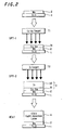
- Japanese Laid-Open Patent Publication No. Hei-10-135495 describes a metal precursor which is formed by sputtering first with a target of Cu-Ga alloy and then with a target of pure indium. As shown in Fig. 2 , a thin firm of CIG for a light absorbing layer 4 is formed on a Mo electrode layer 2 deposited on a SLG (soda lime glass) substrate 1.
- a Cu-Ga metal thin layer 31 is first deposited on the Mo-electrode layer of the substrate by the first sputtering process SPT-1 using the Cu-Ga alloy target and then an In metal thin layer 32 on the Cu-Ga layer 31 by the second sputtering process SPT-2 using the In target to produce a metal-laminated precursor 3' which is then treated by heat in the presence of Selenium (Se) gas to obtain a light absorbing film 4 in the form of a thin CIGS film.
- SPT-1 the first sputtering process SPT-1 using the Cu-Ga alloy target
- an In metal thin layer 32 on the Cu-Ga layer 31 by the second sputtering process SPT-2 using the In target to produce a metal-laminated precursor 3' which is then treated by heat in the presence of Selenium (Se) gas to obtain a light absorbing film 4 in the form of a thin CIGS film.
- Se Selenium
- this precursor 3' being a laminate of a Cu-Ga alloy layer 31 and a sole In layer 32 may be subjected to solid-state diffusion of elements which react with one another to form an alloy Cu-In-Ga at a boundary between the laminated layers both in process of forming the precursor and in the state of being temporarily stored.
- This reaction progresses during the selenization of the precursor.
- the quality of samples of the light absorbing layers 4 may considerably vary. The aggregation of indium is apt to occur, resulting in uneven composition in the layer.
- Hei-10--330936 there is disclosed an opposite target type sputtering apparatus for high-speed formation of films on a cooled substrate by using a pair of opposite targets of the same material, in which a space between the paired target is surrounded by a magnetic field to collect sputter plasma therein and deposit a film on the substrate disposed as facing to one of open sides of the space between the targets.
- an object of the present invention is to provide a method of forming a thin-film light absorbing layer by first forming a precursor film of Ib-IIIb group metals by sputtering and then treating by heat the precursor in an atmosphere of selenium to produce a thin-film of CGIS, wherein the precursor is formed by simultaneously sputtering from a pair of different metal targets disposed opposite to each other to deposit a mixture of sputtered particles on a Mo layer formed on a substrate.
- This precursor has a well mixed single-layered (not laminated) structure, which is free from alloying reaction of elements at a boundary of layers of a laminated precursor obtained by the conventional method.
- Another object of the present invention is to provide a method of forming a light absorbing layer of a solar cell, whereby a thin-film single-layered (i.e., not laminated) precursor is formed by simultaneously supplying Ib group metals and IIIb group metals and then subjected to heat-treatment in an atmosphere of selenium gas.
- the single-layered precursor can be free from the reaction of alloying elements at a boundary between layers of a laminated precursor obtained by the conventional method.
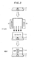
- a light absorbing thin layer fabricating method comprises a sputtering process FT-SPT for forming a metal precursor film 3 of Cu-Ga-In on a molybdenum (Mo) electrode layer 2 formed on a soda-lime glass (SLG) substrate 1 by depositing a mixture of particles sputtered at the same time from a pair of a copper-gallium (Cu-Ga) target T1 and an indium (In) target T2, disposed opposite to each other, and a heat treatment process HEAT for treating by heat the precursor film deposited on the Mo layer of the SLG substrate in a selenium atmosphere to complete the light absorbing layer 4 of CIGS.
- a sputtering process FT-SPT for forming a metal precursor film 3 of Cu-Ga-In on a molybdenum (Mo) electrode layer 2 formed on a soda-lime glass (SLG) substrate 1 by depositing a mixture of particles sputtered at the same time from a pair of a
- Fig. 4 illustrates the state of particles sputtered from the Cu-GA target T1 and the In target T2 when forming a single layer metal precursor 3 of mixed particles of Cu-GA-In.
- the metal precursor 3 obtained by the method according to the present invention is composed of well mixed particles Cu-Ga-In deposited in a single layer whereas the metal cursor obtained by the conventional method are laminated of a thin layer of Cu-Ga and a thin layer of In.
- the metal precursor 3 of the present invention possesses the uniform distribution therein of metal elements Cu, Ga and In, which can prevent the progress of forming an alloy by diffusion of metal elements in solid layers.
- the precursor 3 thus obtained can be evenly selenized by the proceeding heat treatment process.
- the precursor thus formed and treated by heat to form the light absorbing layer can also prevent the occurrence of different crystal layer (different from the crystal structure to be expected) in the thin film compound semiconductor solar cell (a final product), which is a factor of deterioration of the solar cell.
- the precursor 3 has a pseudo amorphous structure which is effective to achieve a high quality of a thin CISG film of the light absorbing layer.
- the metal precursor 3 is an alloy composed of three metal elements, which can prevent the product solar cell from being short-circuited.
- the above-described simultaneous sputtering of both targets T1 and T2 makes it possible to form the precursor 3 at a high speed.
- the precursor thus formed in a single thin layer composed of three metals (Cu, Ga, In) uniformly distributed therein is then treated by heat in an atmosphere of selenium (Se) to form a selenized thin-film of Cu (In+Ga) Se2, which is a light-absorbing layer (p-type semiconductor) possessing a high quality and high performance.
- the solar cell product having a light-absorbing layer 4 thus formed according to the present invention has been proved to show a power conversion efficiency exceeding 15%.
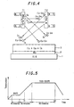
- Fig. 5 shows an example of a heating temperature characteristic of a furnace wherein the precursor is treated by heat with H2Se gas (diluted with 5% argon gas) to form a CIGS thin film light-absorbing layer 4 by thermal chemical reaction with selenium (in gas phase).
- the furnace is first heated up to 100°C following by holding for 10 minutes for stabilizing the inside temperature of the furnace.
- the inside temperature is then increased gradually through a stable ramp-up period of about 30 minutes to 500 ⁇ 520°C at which the soda-lime glass (SLG) substrate with a precursor formed thereon may not be deformed and can be heat-treated to obtain the high quality crystal structure of the precursor.
- H2Se gas diluted with 5% argon gas
- selenium (Se) produced by thermal decomposition of H2Se gas is supplied from the time T1 when the inside temperature of the furnace reached to 230 ⁇ 250°C.
- the precursor of the substrate is treated for 40 minutes maintaining the furnace inside temperature of 500 to 520°C.
- the furnace is charged with H2Se gas from the time point T1 when the inside temperature reached 100°C.
- the precursor is treated by heat at a constant inside pressure of the furnace.
- the furnace gas is replaced by argon gas at a low pressure of about 100 Pa to prevent further unnecessary deposition of selenium.
- Fig. 6 illustrates an example of equipment for mass production of light-absorbing layers of solar cells by applying the light-absorbing layer forming method according to the present invention.
- the equipment comprises an inline thin-film forming apparatus A which includes a substrate feeding chamber P1 provided with a heater for storing a number of substrates 6 (SLG substrates each with a molybdenum electrode layer formed thereon) at a constant temperature and subsequently feeding the substrates 6, a precursor forming chamber P2 for forming a metal precursor layer on each of substrates 6 subsequently fed from the substrate feeding chamber P1 and placed by one at two sputtering portions SPT1 and SPT2 each provided with a pair of oppositely disposed targets T1 and T2 for simultaneously sputtering elements from the respective metal targets and a substrate cooling chamber P3 for receiving the substrates each with a precursor formed thereon from the precursor forming chamber P2 and temporarily storing and cooling the substrates; and an annealing apparatus B in which a number of the precursor-formed substrates 6' cooled and
- Transport of the substrates 6 and 6' is conducted by a transporting mechanism operable under the control from a controller (not shown) in synchronism with the operation of the respective sputtering portions SPT1 and SPT2.
- a controller not shown
- Transport of the substrates 6 and 6' is conducted by a transporting mechanism operable under the control from a controller (not shown) in synchronism with the operation of the respective sputtering portions SPT1 and SPT2.
- paired opposite targets not limited to a combination of Cu-Ga and In targets, other combinations of Cu-Ga and In targets, Cu and In or Al, and Cu and In-Cu.
- paired opposite targets not limited to a combination of Cu-Ga and In targets, other combinations of Cu-Ga and In targets, Cu and In or Al, and Cu and In-Cu.
- the light-absorbing layer forming method can produce a thin-film CIGS light-absorbing layer by forming a thin-film precursor of Ib-IIIb group metals by sputtering and treating by heat the precursor in a selenium atmosphere, wherein particles are sputtered from a pair of oppositely disposed targets, one is a carrier of an alloy Ib group-IIIb group metals and the other is a carrier of single Ib group metal or IIIb group metal, and well mixed to form a thin-film single-layered precursor featured by even distribution therein metal elements sputtered from respective target materials, which precursor can also uniformly selenized by the following heat-treatment process.
- the application of the above-described method makes it possible to form a high quality light-absorbing layer at a high speed and can thereby contribute to improve the productivity of compound semiconductor solar cells.
- a light-absorbing layer of a compound semiconductor solar cell can be produced by a process of forming a thin single layer of an alloy precursor by simultaneously sputtering Ib group metal element and IIIb group metal element and by a proceeding process of selenizing the formed precursor by exposing to selenium gas, wherein the thin-film precursor formed with well mixed Ib group and IIIb group metal elements and then uniformly selenized.
- the above method makes it possible to form a high-quality light-absorbing layer for a solar cell at a high speed and can thereby increase the productivity of compound semiconductor solar cells.
Applications Claiming Priority (5)
| Application Number | Priority Date | Filing Date | Title |
|---|---|---|---|
| JP2001244973 | 2001-07-06 | ||
| JP2001244973 | 2001-07-06 | ||
| JP2001348084 | 2001-10-10 | ||
| JP2001348084 | 2001-10-10 | ||
| PCT/JP2002/005730 WO2003005456A1 (en) | 2001-07-06 | 2002-06-10 | Method for forming light-absorbing layer |
Publications (4)
| Publication Number | Publication Date |
|---|---|
| EP1424735A1 EP1424735A1 (en) | 2004-06-02 |
| EP1424735A8 EP1424735A8 (en) | 2005-04-13 |
| EP1424735A4 EP1424735A4 (en) | 2008-08-20 |
| EP1424735B1 true EP1424735B1 (en) | 2010-07-28 |
Family
ID=26620446
Family Applications (1)
| Application Number | Title | Priority Date | Filing Date |
|---|---|---|---|
| EP02733434A Expired - Fee Related EP1424735B1 (en) | 2001-07-06 | 2002-06-10 | Method for forming light-absorbing layer |
Country Status (5)
| Country | Link |
|---|---|
| US (1) | US20050006221A1 (ja) |
| EP (1) | EP1424735B1 (ja) |
| JP (1) | JP3811825B2 (ja) |
| DE (1) | DE60237159D1 (ja) |
| WO (1) | WO2003005456A1 (ja) |
Families Citing this family (31)
| Publication number | Priority date | Publication date | Assignee | Title |
|---|---|---|---|---|
| DE112005000785T5 (de) * | 2004-04-09 | 2007-03-01 | Honda Motor Co., Ltd. | Verfahren zur Herstellung einer Licht-absorbierenden Schicht für eine Dünnschichtsolarzelle des Chalkopyrittyps |
| US7833821B2 (en) * | 2005-10-24 | 2010-11-16 | Solopower, Inc. | Method and apparatus for thin film solar cell manufacturing |
| KR20100051586A (ko) * | 2007-09-11 | 2010-05-17 | 센트로테에름 포토볼타익스 아게 | 금속 전구체층을 반도체층으로 열적 변환하기 위한 방법 및 장치, 그리고 태양광 모듈 |
| US8779283B2 (en) * | 2007-11-29 | 2014-07-15 | General Electric Company | Absorber layer for thin film photovoltaics and a solar cell made therefrom |
| JP4620105B2 (ja) * | 2007-11-30 | 2011-01-26 | 昭和シェル石油株式会社 | Cis系薄膜太陽電池の光吸収層の製造方法 |
| US7842534B2 (en) * | 2008-04-02 | 2010-11-30 | Sunlight Photonics Inc. | Method for forming a compound semi-conductor thin-film |
| CN101807620B (zh) * | 2009-02-17 | 2015-05-13 | 通用电气公司 | 用于薄膜光伏的吸收层及由其制成的太阳能电池 |
| AU2009200640B2 (en) * | 2009-02-18 | 2015-02-05 | General Electric Company | Absorber layer for thin film photovoltaics and a solar cell made therefrom |
| JP2010192690A (ja) * | 2009-02-18 | 2010-09-02 | Tdk Corp | 太陽電池の製造方法 |
| JP2010232608A (ja) * | 2009-03-30 | 2010-10-14 | Honda Motor Co Ltd | カルコパイライト型太陽電池の製造方法 |
| US20110023750A1 (en) * | 2009-07-28 | 2011-02-03 | Kuan-Che Wang | Ink composition for forming absorbers of thin film cells and producing method thereof |
| KR101271753B1 (ko) * | 2009-11-20 | 2013-06-05 | 한국전자통신연구원 | 박막형 광 흡수층의 제조 방법, 이를 이용한 박막 태양전지 제조 방법 및 박막 태양전지 |
| DE102009047483A1 (de) * | 2009-12-04 | 2011-06-09 | Sulfurcell Solartechnik Gmbh | Vorrichtung und Verfahren zur Erzeugung von Chalkopyrit-Absorberschichten in Solarzellen |
| CN101814553B (zh) * | 2010-03-05 | 2011-10-05 | 中国科学院上海硅酸盐研究所 | 光辅助方法制备铜铟镓硒薄膜太阳电池光吸收层 |
| JP5837564B2 (ja) | 2010-03-17 | 2015-12-24 | ダウ グローバル テクノロジーズ エルエルシー | カルコゲン含有光吸収性構造体を製造する方法および光起電力装置 |
| CN102024870B (zh) * | 2010-04-19 | 2013-07-24 | 福建欧德生光电科技有限公司 | 半导体薄膜太阳能电池的制造系统和方法 |
| KR20110128580A (ko) | 2010-05-24 | 2011-11-30 | 삼성전자주식회사 | 태양 전지 제조 방법 |
| TWI508179B (zh) * | 2010-07-23 | 2015-11-11 | Sunshine Pv Corp | 薄膜太陽能電池的退火裝置 |
| US20120034764A1 (en) * | 2010-08-05 | 2012-02-09 | Aventa Technologies Llc | System and method for fabricating thin-film photovoltaic devices |
| US20120034733A1 (en) * | 2010-08-05 | 2012-02-09 | Aventa Technologies Llc | System and method for fabricating thin-film photovoltaic devices |
| JP2012079997A (ja) * | 2010-10-05 | 2012-04-19 | Kobe Steel Ltd | 化合物半導体薄膜太陽電池用光吸収層の製造方法、およびIn−Cu合金スパッタリングターゲット |
| EP2487722A1 (en) | 2011-01-19 | 2012-08-15 | Hitachi, Ltd. | Light absorption layer |
| EA020377B1 (ru) * | 2011-05-12 | 2014-10-30 | Общество С Ограниченной Ответственностью "Изовак" | Способ формирования тонких пленок cigs для солнечных батарей и устройство для его реализации |
| CN102214735A (zh) * | 2011-06-11 | 2011-10-12 | 蚌埠玻璃工业设计研究院 | 一种铜铟镓硒/硫太阳电池吸收层的制备方法 |
| US8642884B2 (en) * | 2011-09-09 | 2014-02-04 | International Business Machines Corporation | Heat treatment process and photovoltaic device based on said process |
| US9082619B2 (en) * | 2012-07-09 | 2015-07-14 | International Solar Electric Technology, Inc. | Methods and apparatuses for forming semiconductor films |
| KR101521450B1 (ko) * | 2013-01-28 | 2015-05-21 | 조선대학교산학협력단 | CuSe2를 타겟으로 하는 비셀렌화 스퍼터링 공정을 이용한 CIGS 박막 제조방법 |
| US10840400B2 (en) * | 2013-08-29 | 2020-11-17 | Taiwan Semiconductor Manufacturing Co., Ltd. | Photovoltaic device with back reflector |
| CN104393111A (zh) * | 2014-10-31 | 2015-03-04 | 徐东 | 一种cigs太阳能电池吸收层的制备方法 |
| CN104300014A (zh) * | 2014-10-31 | 2015-01-21 | 徐东 | 一种cigs太阳能电池吸收层的制备设备及其制备方法 |
| CN104538492A (zh) * | 2014-12-11 | 2015-04-22 | 兰州空间技术物理研究所 | 一种铜铟镓硒薄膜太阳电池光吸收层薄膜的制备方法 |
Citations (2)
| Publication number | Priority date | Publication date | Assignee | Title |
|---|---|---|---|---|
| US5000834A (en) * | 1989-02-17 | 1991-03-19 | Pioneer Electronic Corporation | Facing targets sputtering device |
| EP0838864A2 (en) * | 1996-10-25 | 1998-04-29 | Showa Shell Sekiyu Kabushiki Kaisha | Method for producing thin-film solar cell and equipment for producing the same |
Family Cites Families (14)
| Publication number | Priority date | Publication date | Assignee | Title |
|---|---|---|---|---|
| US4798660A (en) * | 1985-07-16 | 1989-01-17 | Atlantic Richfield Company | Method for forming Cu In Se2 films |
| US5439575A (en) * | 1988-06-30 | 1995-08-08 | Board Of Trustees Of The University Of Illinois | Hybrid method for depositing semi-conductive materials |
| US4915745A (en) * | 1988-09-22 | 1990-04-10 | Atlantic Richfield Company | Thin film solar cell and method of making |
| US4990229A (en) * | 1989-06-13 | 1991-02-05 | Plasma & Materials Technologies, Inc. | High density plasma deposition and etching apparatus |
| JPH03268335A (ja) * | 1990-03-16 | 1991-11-29 | Fuji Electric Corp Res & Dev Ltd | カルコパイライト系化合物膜の生成方法 |
| JPH0539562A (ja) * | 1991-08-06 | 1993-02-19 | Fuji Electric Corp Res & Dev Ltd | CuInSe2 薄膜の形成方法 |
| JPH05166726A (ja) * | 1991-12-19 | 1993-07-02 | Matsushita Electric Ind Co Ltd | 化合物薄膜の製造方法 |
| JPH05182911A (ja) * | 1991-12-27 | 1993-07-23 | Hitachi Ltd | スパッタ装置 |
| US5667650A (en) * | 1995-02-14 | 1997-09-16 | E. I. Du Pont De Nemours And Company | High flow gas manifold for high rate, off-axis sputter deposition |
| JP3886209B2 (ja) * | 1997-06-02 | 2007-02-28 | 貞夫 門倉 | 対向ターゲット式スパッタ装置 |
| US6323417B1 (en) * | 1998-09-29 | 2001-11-27 | Lockheed Martin Corporation | Method of making I-III-VI semiconductor materials for use in photovoltaic cells |
| JP4389076B2 (ja) * | 1999-04-16 | 2009-12-24 | 本田技研工業株式会社 | 化合物成膜方法および装置 |
| JP2001035861A (ja) * | 1999-07-23 | 2001-02-09 | Matsushita Electric Ind Co Ltd | 薄膜の製造方法および製造装置 |
| JP3831592B2 (ja) * | 2000-09-06 | 2006-10-11 | 松下電器産業株式会社 | 化合物半導体薄膜の製造方法 |
-
2002
- 2002-06-10 EP EP02733434A patent/EP1424735B1/en not_active Expired - Fee Related
- 2002-06-10 DE DE60237159T patent/DE60237159D1/de not_active Expired - Lifetime
- 2002-06-10 WO PCT/JP2002/005730 patent/WO2003005456A1/ja active Application Filing
- 2002-06-10 US US10/482,750 patent/US20050006221A1/en not_active Abandoned
- 2002-06-10 JP JP2003511320A patent/JP3811825B2/ja not_active Expired - Fee Related
Patent Citations (2)
| Publication number | Priority date | Publication date | Assignee | Title |
|---|---|---|---|---|
| US5000834A (en) * | 1989-02-17 | 1991-03-19 | Pioneer Electronic Corporation | Facing targets sputtering device |
| EP0838864A2 (en) * | 1996-10-25 | 1998-04-29 | Showa Shell Sekiyu Kabushiki Kaisha | Method for producing thin-film solar cell and equipment for producing the same |
Also Published As
| Publication number | Publication date |
|---|---|
| EP1424735A8 (en) | 2005-04-13 |
| US20050006221A1 (en) | 2005-01-13 |
| EP1424735A1 (en) | 2004-06-02 |
| DE60237159D1 (de) | 2010-09-09 |
| JPWO2003005456A1 (ja) | 2004-10-28 |
| WO2003005456A1 (en) | 2003-01-16 |
| JP3811825B2 (ja) | 2006-08-23 |
| EP1424735A4 (en) | 2008-08-20 |
Similar Documents
| Publication | Publication Date | Title |
|---|---|---|
| EP1424735B1 (en) | Method for forming light-absorbing layer | |
| US7576017B2 (en) | Method and apparatus for forming a thin-film solar cell using a continuous process | |
| EP2260506B1 (en) | Method for forming a compound semi-conductor thin-film | |
| US9614118B2 (en) | Method and apparatus for depositing copper-indium-gallium selenide (CuInGaSe2-cigs) thin films and other materials on a substrate | |
| CN100456502C (zh) | 黄铜矿型薄膜太阳能电池用光吸收层的制造方法 | |
| JP3897622B2 (ja) | 化合物半導体薄膜の製造方法 | |
| CA2586966A1 (en) | Method and apparatus for forming a thin-film solar cell using a continuous process | |
| CN103021805B (zh) | 使用溅射和蒸发功能形成硫族化合物半导体材料的方法和系统 | |
| WO2007121383A2 (en) | Method and apparatus to form thin layers of materials on a base | |
| JPH06151930A (ja) | カルコパイライト型化合物薄膜の製造方法 | |
| JP4110515B2 (ja) | 薄膜太陽電池およびその製造方法 | |
| US20100065418A1 (en) | Reactive magnetron sputtering for the large-scale deposition of chalcopyrite absorber layers for thin layer solar cells | |
| JP2002083824A (ja) | 化合物半導体薄膜ならびにその製造方法および製造装置 | |
| JP4320525B2 (ja) | 光吸収層の作製方法および装置 | |
| JP2003282600A (ja) | 光吸収層の作製方法および装置 | |
| JPH06120545A (ja) | 薄膜太陽電池の製造方法 | |
| US20120034734A1 (en) | System and method for fabricating thin-film photovoltaic devices | |
| JP2004031551A (ja) | 化合物半導体薄膜の製造方法 | |
| WO2011052574A1 (ja) | カルコパイライト型化合物薄膜の製造方法およびそれを用いた薄膜太陽電池の製造方法 | |
| KR101237466B1 (ko) | 셀렌화에 의한 광흡수층 제조장치 | |
| JP2003188396A (ja) | 光吸収層の形成方法および装置 | |
| US20120034733A1 (en) | System and method for fabricating thin-film photovoltaic devices | |
| US20170236710A1 (en) | Machine and process for continuous, sequential, deposition of semiconductor solar absorbers having variable semiconductor composition deposited in multiple sublayers | |
| US20130224904A1 (en) | Method for fabricating thin-film photovoltaic devices | |
| JPH08195499A (ja) | カルコパイライト化合物薄膜の製造方法 |
Legal Events
| Date | Code | Title | Description |
|---|---|---|---|
| PUAI | Public reference made under article 153(3) epc to a published international application that has entered the european phase |
Free format text: ORIGINAL CODE: 0009012 |
|
| 17P | Request for examination filed |
Effective date: 20040202 |
|
| AK | Designated contracting states |
Kind code of ref document: A1 Designated state(s): AT BE CH CY DE DK ES FI FR GB GR IE IT LI LU MC NL PT SE TR |
|
| AX | Request for extension of the european patent |
Extension state: AL LT LV MK RO SI |
|
| RTI1 | Title (correction) |
Free format text: METHOD FOR FORMING LIGHT-ABSORBING LAYER |
|
| A4 | Supplementary search report drawn up and despatched |
Effective date: 20080722 |
|
| RIC1 | Information provided on ipc code assigned before grant |
Ipc: C23C 14/34 20060101ALI20080716BHEP Ipc: H01L 31/032 20060101AFI20080716BHEP Ipc: C23C 14/06 20060101ALI20080716BHEP |
|
| 17Q | First examination report despatched |
Effective date: 20090220 |
|
| GRAP | Despatch of communication of intention to grant a patent |
Free format text: ORIGINAL CODE: EPIDOSNIGR1 |
|
| GRAS | Grant fee paid |
Free format text: ORIGINAL CODE: EPIDOSNIGR3 |
|
| GRAA | (expected) grant |
Free format text: ORIGINAL CODE: 0009210 |
|
| RIN1 | Information on inventor provided before grant (corrected) |
Inventor name: KOMARU, TAKASHI, Inventor name: KUME, TOMOYUKI, Inventor name: TAKEUCHI, NOBUYOSHI |
|
| AK | Designated contracting states |
Kind code of ref document: B1 Designated state(s): DE SE |
|
| REF | Corresponds to: |
Ref document number: 60237159 Country of ref document: DE Date of ref document: 20100909 Kind code of ref document: P |
|
| REG | Reference to a national code |
Ref country code: SE Ref legal event code: TRGR |
|
| PLBE | No opposition filed within time limit |
Free format text: ORIGINAL CODE: 0009261 |
|
| STAA | Information on the status of an ep patent application or granted ep patent |
Free format text: STATUS: NO OPPOSITION FILED WITHIN TIME LIMIT |
|
| 26N | No opposition filed |
Effective date: 20110429 |
|
| PGFP | Annual fee paid to national office [announced via postgrant information from national office to epo] |
Ref country code: SE Payment date: 20110613 Year of fee payment: 10 |
|
| REG | Reference to a national code |
Ref country code: DE Ref legal event code: R097 Ref document number: 60237159 Country of ref document: DE Effective date: 20110429 |
|
| REG | Reference to a national code |
Ref country code: SE Ref legal event code: EUG |
|
| PG25 | Lapsed in a contracting state [announced via postgrant information from national office to epo] |
Ref country code: SE Free format text: LAPSE BECAUSE OF NON-PAYMENT OF DUE FEES Effective date: 20120611 |
|
| PGFP | Annual fee paid to national office [announced via postgrant information from national office to epo] |
Ref country code: DE Payment date: 20140603 Year of fee payment: 13 |
|
| REG | Reference to a national code |
Ref country code: DE Ref legal event code: R119 Ref document number: 60237159 Country of ref document: DE |
|
| PG25 | Lapsed in a contracting state [announced via postgrant information from national office to epo] |
Ref country code: DE Free format text: LAPSE BECAUSE OF NON-PAYMENT OF DUE FEES Effective date: 20160101 |