EP1415483B1 - Dispositif de commutation optique - Google Patents
Dispositif de commutation optique Download PDFInfo
- Publication number
- EP1415483B1 EP1415483B1 EP02749097A EP02749097A EP1415483B1 EP 1415483 B1 EP1415483 B1 EP 1415483B1 EP 02749097 A EP02749097 A EP 02749097A EP 02749097 A EP02749097 A EP 02749097A EP 1415483 B1 EP1415483 B1 EP 1415483B1
- Authority
- EP
- European Patent Office
- Prior art keywords
- polarisation
- polariser
- light
- switchable
- mode
- Prior art date
- Legal status (The legal status is an assumption and is not a legal conclusion. Google has not performed a legal analysis and makes no representation as to the accuracy of the status listed.)
- Expired - Lifetime
Links
Images


Classifications
-
- G—PHYSICS
- G02—OPTICS
- G02F—OPTICAL DEVICES OR ARRANGEMENTS FOR THE CONTROL OF LIGHT BY MODIFICATION OF THE OPTICAL PROPERTIES OF THE MEDIA OF THE ELEMENTS INVOLVED THEREIN; NON-LINEAR OPTICS; FREQUENCY-CHANGING OF LIGHT; OPTICAL LOGIC ELEMENTS; OPTICAL ANALOGUE/DIGITAL CONVERTERS
- G02F1/00—Devices or arrangements for the control of the intensity, colour, phase, polarisation or direction of light arriving from an independent light source, e.g. switching, gating or modulating; Non-linear optics
- G02F1/01—Devices or arrangements for the control of the intensity, colour, phase, polarisation or direction of light arriving from an independent light source, e.g. switching, gating or modulating; Non-linear optics for the control of the intensity, phase, polarisation or colour
- G02F1/13—Devices or arrangements for the control of the intensity, colour, phase, polarisation or direction of light arriving from an independent light source, e.g. switching, gating or modulating; Non-linear optics for the control of the intensity, phase, polarisation or colour based on liquid crystals, e.g. single liquid crystal display cells
- G02F1/1326—Liquid crystal optical waveguides or liquid crystal cells specially adapted for gating or modulating between optical waveguides
-
- G—PHYSICS
- G02—OPTICS
- G02B—OPTICAL ELEMENTS, SYSTEMS OR APPARATUS
- G02B30/00—Optical systems or apparatus for producing three-dimensional [3D] effects, e.g. stereoscopic images
- G02B30/20—Optical systems or apparatus for producing three-dimensional [3D] effects, e.g. stereoscopic images by providing first and second parallax images to an observer's left and right eyes
- G02B30/22—Optical systems or apparatus for producing three-dimensional [3D] effects, e.g. stereoscopic images by providing first and second parallax images to an observer's left and right eyes of the stereoscopic type
- G02B30/25—Optical systems or apparatus for producing three-dimensional [3D] effects, e.g. stereoscopic images by providing first and second parallax images to an observer's left and right eyes of the stereoscopic type using polarisation techniques
-
- G—PHYSICS
- G02—OPTICS
- G02B—OPTICAL ELEMENTS, SYSTEMS OR APPARATUS
- G02B30/00—Optical systems or apparatus for producing three-dimensional [3D] effects, e.g. stereoscopic images
- G02B30/20—Optical systems or apparatus for producing three-dimensional [3D] effects, e.g. stereoscopic images by providing first and second parallax images to an observer's left and right eyes
- G02B30/26—Optical systems or apparatus for producing three-dimensional [3D] effects, e.g. stereoscopic images by providing first and second parallax images to an observer's left and right eyes of the autostereoscopic type
- G02B30/27—Optical systems or apparatus for producing three-dimensional [3D] effects, e.g. stereoscopic images by providing first and second parallax images to an observer's left and right eyes of the autostereoscopic type involving lenticular arrays
-
- G—PHYSICS
- G02—OPTICS
- G02F—OPTICAL DEVICES OR ARRANGEMENTS FOR THE CONTROL OF LIGHT BY MODIFICATION OF THE OPTICAL PROPERTIES OF THE MEDIA OF THE ELEMENTS INVOLVED THEREIN; NON-LINEAR OPTICS; FREQUENCY-CHANGING OF LIGHT; OPTICAL LOGIC ELEMENTS; OPTICAL ANALOGUE/DIGITAL CONVERTERS
- G02F1/00—Devices or arrangements for the control of the intensity, colour, phase, polarisation or direction of light arriving from an independent light source, e.g. switching, gating or modulating; Non-linear optics
- G02F1/01—Devices or arrangements for the control of the intensity, colour, phase, polarisation or direction of light arriving from an independent light source, e.g. switching, gating or modulating; Non-linear optics for the control of the intensity, phase, polarisation or colour
- G02F1/13—Devices or arrangements for the control of the intensity, colour, phase, polarisation or direction of light arriving from an independent light source, e.g. switching, gating or modulating; Non-linear optics for the control of the intensity, phase, polarisation or colour based on liquid crystals, e.g. single liquid crystal display cells
- G02F1/133—Constructional arrangements; Operation of liquid crystal cells; Circuit arrangements
- G02F1/1333—Constructional arrangements; Manufacturing methods
- G02F1/1335—Structural association of cells with optical devices, e.g. polarisers or reflectors
- G02F1/133526—Lenses, e.g. microlenses or Fresnel lenses
-
- H—ELECTRICITY
- H04—ELECTRIC COMMUNICATION TECHNIQUE
- H04N—PICTORIAL COMMUNICATION, e.g. TELEVISION
- H04N13/00—Stereoscopic video systems; Multi-view video systems; Details thereof
- H04N13/30—Image reproducers
- H04N13/302—Image reproducers for viewing without the aid of special glasses, i.e. using autostereoscopic displays
- H04N13/305—Image reproducers for viewing without the aid of special glasses, i.e. using autostereoscopic displays using lenticular lenses, e.g. arrangements of cylindrical lenses
-
- H—ELECTRICITY
- H04—ELECTRIC COMMUNICATION TECHNIQUE
- H04N—PICTORIAL COMMUNICATION, e.g. TELEVISION
- H04N13/00—Stereoscopic video systems; Multi-view video systems; Details thereof
- H04N13/30—Image reproducers
- H04N13/302—Image reproducers for viewing without the aid of special glasses, i.e. using autostereoscopic displays
- H04N13/31—Image reproducers for viewing without the aid of special glasses, i.e. using autostereoscopic displays using parallax barriers
-
- H—ELECTRICITY
- H04—ELECTRIC COMMUNICATION TECHNIQUE
- H04N—PICTORIAL COMMUNICATION, e.g. TELEVISION
- H04N13/00—Stereoscopic video systems; Multi-view video systems; Details thereof
- H04N13/30—Image reproducers
- H04N13/356—Image reproducers having separate monoscopic and stereoscopic modes
- H04N13/359—Switching between monoscopic and stereoscopic modes
-
- H—ELECTRICITY
- H04—ELECTRIC COMMUNICATION TECHNIQUE
- H04N—PICTORIAL COMMUNICATION, e.g. TELEVISION
- H04N13/00—Stereoscopic video systems; Multi-view video systems; Details thereof
- H04N13/30—Image reproducers
- H04N13/361—Reproducing mixed stereoscopic images; Reproducing mixed monoscopic and stereoscopic images, e.g. a stereoscopic image overlay window on a monoscopic image background
-
- H—ELECTRICITY
- H04—ELECTRIC COMMUNICATION TECHNIQUE
- H04N—PICTORIAL COMMUNICATION, e.g. TELEVISION
- H04N13/00—Stereoscopic video systems; Multi-view video systems; Details thereof
- H04N13/30—Image reproducers
- H04N13/398—Synchronisation thereof; Control thereof
-
- G—PHYSICS
- G02—OPTICS
- G02F—OPTICAL DEVICES OR ARRANGEMENTS FOR THE CONTROL OF LIGHT BY MODIFICATION OF THE OPTICAL PROPERTIES OF THE MEDIA OF THE ELEMENTS INVOLVED THEREIN; NON-LINEAR OPTICS; FREQUENCY-CHANGING OF LIGHT; OPTICAL LOGIC ELEMENTS; OPTICAL ANALOGUE/DIGITAL CONVERTERS
- G02F1/00—Devices or arrangements for the control of the intensity, colour, phase, polarisation or direction of light arriving from an independent light source, e.g. switching, gating or modulating; Non-linear optics
- G02F1/01—Devices or arrangements for the control of the intensity, colour, phase, polarisation or direction of light arriving from an independent light source, e.g. switching, gating or modulating; Non-linear optics for the control of the intensity, phase, polarisation or colour
- G02F1/13—Devices or arrangements for the control of the intensity, colour, phase, polarisation or direction of light arriving from an independent light source, e.g. switching, gating or modulating; Non-linear optics for the control of the intensity, phase, polarisation or colour based on liquid crystals, e.g. single liquid crystal display cells
- G02F1/133—Constructional arrangements; Operation of liquid crystal cells; Circuit arrangements
- G02F1/1333—Constructional arrangements; Manufacturing methods
- G02F1/1347—Arrangement of liquid crystal layers or cells in which the final condition of one light beam is achieved by the addition of the effects of two or more layers or cells
- G02F1/13471—Arrangement of liquid crystal layers or cells in which the final condition of one light beam is achieved by the addition of the effects of two or more layers or cells in which all the liquid crystal cells or layers remain transparent, e.g. FLC, ECB, DAP, HAN, TN, STN, SBE-LC cells
-
- G—PHYSICS
- G02—OPTICS
- G02F—OPTICAL DEVICES OR ARRANGEMENTS FOR THE CONTROL OF LIGHT BY MODIFICATION OF THE OPTICAL PROPERTIES OF THE MEDIA OF THE ELEMENTS INVOLVED THEREIN; NON-LINEAR OPTICS; FREQUENCY-CHANGING OF LIGHT; OPTICAL LOGIC ELEMENTS; OPTICAL ANALOGUE/DIGITAL CONVERTERS
- G02F2202/00—Materials and properties
- G02F2202/40—Materials having a particular birefringence, retardation
-
- G—PHYSICS
- G02—OPTICS
- G02F—OPTICAL DEVICES OR ARRANGEMENTS FOR THE CONTROL OF LIGHT BY MODIFICATION OF THE OPTICAL PROPERTIES OF THE MEDIA OF THE ELEMENTS INVOLVED THEREIN; NON-LINEAR OPTICS; FREQUENCY-CHANGING OF LIGHT; OPTICAL LOGIC ELEMENTS; OPTICAL ANALOGUE/DIGITAL CONVERTERS
- G02F2203/00—Function characteristic
- G02F2203/07—Polarisation dependent
-
- Y—GENERAL TAGGING OF NEW TECHNOLOGICAL DEVELOPMENTS; GENERAL TAGGING OF CROSS-SECTIONAL TECHNOLOGIES SPANNING OVER SEVERAL SECTIONS OF THE IPC; TECHNICAL SUBJECTS COVERED BY FORMER USPC CROSS-REFERENCE ART COLLECTIONS [XRACs] AND DIGESTS
- Y10—TECHNICAL SUBJECTS COVERED BY FORMER USPC
- Y10S—TECHNICAL SUBJECTS COVERED BY FORMER USPC CROSS-REFERENCE ART COLLECTIONS [XRACs] AND DIGESTS
- Y10S385/00—Optical waveguides
- Y10S385/901—Illuminating or display apparatus
Definitions
- the present invention relates to optical switching processes and apparatus.
- Such an apparatus may be used in a switchable two dimensional (2D)/three dimensional (3D) autostereoscopic display apparatus; for a switchable high brightness reflective display system; for a multi-user display system; or for a directional lighting system
- Such systems may be used in computer monitors, telecommunications handsets, digital cameras, laptop and desktop computers, games apparatuses, automotive and other mobile display applications as well as telecommunications switching applications.
- Normal human vision is stereoscopic, that is each eye sees a slightly different image of the world.
- the brain fuses the two images (referred to as the stereo pair) to give the sensation of depth.
- Three dimensional stereoscopic displays replay a separate, generally planar, image to each of the eyes corresponding to that which would be seen if viewing a real world scene.
- the brain again fuses the stereo pair to give the appearance of depth in the image.
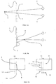
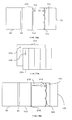
- Fig.1a shows in plan view a display surface in a display plane 1.
- a right eye 2 views a right eye homologous image point 3 on the display plane and a left eye 4 views a left eye homologous point 5 on the display plane to produce an apparent image point 6 perceived by the user behind the screen plane.
- Fig.1b shows in plan view a display surface in a display plane 1.
- a right eye 2 views a right eye homologous image point 7 on the display plane and a left eye 4 views a left eye homologous point 8 on the display plane to produce an apparent image point 9 in front of the screen plane.
- Fig. 1c shows the appearance of the left eye image 10 and right eye image 11.
- the homologous point 5 in the left eye image 10 is positioned on a reference line 12.
- the corresponding homologous point 3 in the right eye image 11 is at a different relative position 3 with respect to the reference line 12.
- the separation 13 of the point 3 from the reference line 12 is called the disparity and in this case is a positive disparity for points which will lie behind the screen plane.
- a generalised point in the scene there is a corresponding point in each image of the stereo pair as shown in fig. 1a. These points are termed the homologous points.
- the relative separation of the homologous points between the two images is termed the disparity; points with zero disparity correspond to points at the depth plane of the display.
- Fig.1b shows that points with uncrossed disparity appear behind the display and fig1c shows that points with crossed disparity appear in front of the display.
- the magnitude of the separation of the homologous points, the distance to the observer, and the observer's interocular separation gives the amount of depth perceived on the display.
- Stereoscopic type displays are well known in the prior art and refer to displays in which some kind of viewing aid is worn by the user to substantially separate the views sent to the left and right eyes.
- the viewing aid may be colour filters in which the images are colour coded (e.g. red and green); polarising glasses in which the images are encoded in orthogonal polarisation states; or shutter glasses in which the views are encoded as a temporal sequence of images in synchronisation with the opening of the shutters of the glasses.
- Autostereoscopic displays operate without viewing aids worn by the observer.
- each of the views can be seen from a limited region in space as illustrated in fig.2.
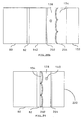
- Fig.2a shows a display device 16 with an attached parallax optical element 17.
- the display device produces a right eye image 18 for the right eye channel.
- the parallax optical element 17 directs light in a direction shown by the arrow 19 to produce a right eye viewing window 20 in the region in front of the display.
- An observer places their right eye 22 at the position of the window 20.
- the position of the left eye viewing window 24 is shown for reference.
- the viewing window 20 may also be referred to as a vertically extended optical pupil.
- Fig.2b shows the left eye optical system.
- the display device 16 produces a left eye image 26 for the left eye channel.
- the parallax optical element 17 directs light in a direction shown by the arrow 28 to produce a left eye viewing window 30 in the region in front of the display. An observer places their left eye 32 at the position of the window 30. The position of the right eye viewing window 20 is shown for reference.
- the system comprises a display and an optical steering mechanism.
- the light from the left image 26 is sent to a limited region in front of the display, referred to as the viewing window 30. If an eye 32 is placed at the position of the viewing window 30 then the observer sees the appropriate image 26 across the whole of the display 16.
- the optical system sends the light intended for the right image 18 to a separate window 20. If the observer places their right eye 22 in that window then the right eye image will be seen across the whole of the display.
- the light from either image may be considered to have been optically steered (i.e. directed) into a respective directional distribution.
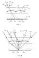
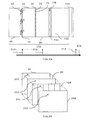
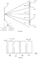
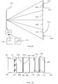
- Fig.3 shows in plan view a display device 16,17 in a display plane 34 producing the left eye viewing windows 36,37,38 and right eye viewing windows 39,40,41 in the window plane 42.
- the separation of the window plane from the display is termed the nominal viewing distance 43.
- the windows 37,40 in the central position with respect to the display are in the zeroth lobe 44.
- Windows 36,39 to the right of the zeroth lobe 44 are in the +1 lobe 46, while windows 38,41 to the left of the zeroth lobe are in the -1 lobe 48.
- the viewing window plane of the display represents the distance from the display at which the lateral viewing freedom is greatest.
- a diamond shaped autostereoscopic viewing zone as illustrated in plan view in fig.3.
- the light from each of the points across the display is beamed in a cone of finite width to the viewing windows.
- the width of the cone may be defined as the angular width.
- the longitudinal viewing freedom of the display is determined by the length of these viewing zones.
- the variation in intensity 50 across the window plane of a display (constituting one tangible form of a directional distribution of the light) is shown with respect to position 51 for idealised windows in fig.4a.
- the right eye window position intensity distribution 52 corresponds to the window 41 in fig.3
- intensity distribution 53 corresponds to the window 37
- intensity distribution 54 corresponds to the window 40
- intensity distribution 55 corresponds to the window 36.
- Fig.4b shows the intensity distribution with position schematically for more realistic windows.
- the right eye window position intensity distribution 56 corresponds to the window 41 in fig.3, and intensity distribution 57 corresponds to the window 37, intensity distribution 58 corresponds to the window 40 and intensity distribution 59 corresponds to the window 36.
- Fig4a shows the ideal viewing windows
- fig.4b is a schematic of the actual viewing windows that may be outputted from the display.
- Several artefacts can occur due to inadequate window performance.
- Cross talk occurs when light from the right eye image is seen by the left eye and vice versa. This is a significant 3D image degradation mechanism which can lead to visual strain for the user.
- poor window quality will lead to a reduction in the viewing freedom of the observer.
- the optical system is designed to optimised the performance of the viewing windows.
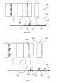
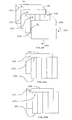
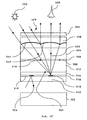
- One type of well known flat panel autostereoscopic display comprises a backlight, an array of electronically adjustable pixels (known as a spatial light modulator, SLM) arranged in columns and rows and a parallax barrier attached to the front of the display as illustrated in plan view in fig.5.
- SLM spatial light modulator
- a backlight 60 produces a light output 62 which is incident on an LCD input polariser 64.
- the light is transmitted through a TFT LCD substrate 66 and is incident on a repeating array of pixels arranged in columns and rows in an LCD pixel plane 67.
- the red pixels 68,71,74, green pixels 69,72,75 and blue pixels 70,73 each comprise an individually controllable liquid crystal layer and are separated by regions of an opaque mask called a black mask 76.
- Each pixel comprises a transmissive region, or pixel aperture 78.
- Light passing through the pixel is modulated in phase by the liquid crystal material in the LCD pixel plane 74 and in colour by a colour filter positioned on an LCD colour filter substrate 80.
- the light then passes through an output polariser 82 after which is placed a parallax barrier 84 and a parallax barrier substrate 86.
- the parallax barrier 84 comprises an array of vertically extended transmissive regions separated by vertically extended opaque regions and serves to direct light from alternate pixel columns 69,71,73,75 to the right eye as shown by the ray 88 for light from pixel 69 and from the intermediate columns 68,70,72,74 to the left eye as shown by the ray 90 (this overall light direction pattern forming another example of a directional distribution of light).
- the observer sees the light from the underlying pixel illuminating the aperture of the barrier, 92.
- an SLM includes both 'light valve' devices such as liquid crystal displays and emissive devices such as electroluminescent displays and LED displays.
- the pixels of the display are arranged as rows and columns separated by gaps, (generally defined by the black mask in a liquid crystal display, LCD) with the parallax barrier being an array of vertically extended slits of pitch close to twice the pitch of the pixel columns.
- the parallax barrier limits the range of angles from which light from each pixel column can be seen, thus creating the viewing windows at a region in front of the display.
- the angles of the output cone from the display are determined by the width and shape of the pixel aperture and the alignment and aberrations of the parallax barrier.
- the pitch of the parallax barrier is slightly smaller than twice the pitch of the pixel array. This condition is known as 'viewpoint correction'.
- the resolution of each of the stereo pair images is half the horizontal resolution of the base LCD, and two views are created.
- the light from the odd columns of pixels 68,70,72,74 can be seen from the left viewing window, and the light from the even columns of pixels 69,71,73,75 can be seen from the right viewing window. If the left eye image data is placed on the odd columns of the display and the right eye image data on the even columns then the observer in the correct 'orthoscopic' position should fuse the two images to see an autostereoscopic 3D image across the whole of the display.
- a parallax barrier type display In a parallax barrier type display, the columns directly under the slits are imaged to a first pair of windows in the zeroeth lobe of the display. The adjacent pixel columns are also imaged to viewing windows, in +1 and -1 lobes of the display.
- the image is termed 'pseudoscopic', compared to the correct orthoscopic condition.
- more than two pixel columns can be placed under each slit of the barrier. For example, four columns will create four windows in which the view is changed for each window. Such a display will give a 'look-around' appearance as the observer moves.
- the longitudinal freedom is also increased by such a method.
- the resolution of the display is limited to one quarter of the resolution of the base panel.
- Parallax barriers rely on blocking the light from regions of the display and therefore reduce the brightness and device efficiency, generally to approximately 20-40% of the original display brightness.
- Parallax barriers are not readily removed and replaced due to the requirements of sub-pixel alignment tolerances of the barrier with respect to the pixel structure of the display in order to optimise the viewing freedom of the display.
- the 2D mode is half resolution.
- the parallax elements may be embodied as slits behind the display, as disclosed in G.Hamagishi et al "A Display System with 2D/3D compatibility", Proc.SID 1998 pp915-918. It can be shown that such a display suffers from Fresnel diffraction artefacts, limiting the quality of the viewing windows that can be obtained.
- the parallax elements may be embodied as light lines interspersed by dark regions as disclosed in US4 717 949. It can be shown that such a display suffers from Fresnel diffraction artefacts, limiting the quality of the viewing windows that can be obtained, G.Woodgate et al Proc.SPIE Vol 3957 "Flat panel autostereoscopic displays - characterisation and enhancement" pp153-164, 2000.
- lenticular screen Another type of parallax optic (cf. parallax barriers) well known in the art for use in stereoscopic displays is called the lenticular screen, which is an array of vertically extended cylindrical microlenses.
- the term "cylindrical” as used herein has its normal meaning in the art and includes not only strictly spherical lens shapes but also aspherical lens shapes.
- the pitch of the lenses again corresponds to the viewpoint correction condition.
- the curvature of the lenses is set substantially so as to produce an image of the LCD pixels at the window plane. As the lenses collect the light in a cone from the pixel and distribute it to the windows, lenticular displays have the full brightness of the base panel.
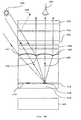
- Fig.6 shows the structure of a prior art lenticular display device.
- the device is configured as described in fig.5 up to the output polariser 82.
- the light then passes through a lenticular screen substrate 94 and a lenticular screen 96 which is formed on the surface of the lenticular screen substrate 92.
- the lenticular screen 94 serves to direct light from alternate pixel columns 69,71,73,75 to the right eye as shown by the ray 88 from the pixel 69 and from the intermediate columns 68,70,72,74 to the left eye as shown by the ray 90 from pixel 68.
- the observer sees the light from the underlying pixel illuminating the aperture of the individual lenticule, 98 of the lenticular screen 96.
- the extent of the captured light cone is shown by the captured rays 100.
- Lenticular displays are described in T.Okoshi "Threee Dimensional Imaging Techniques", Academic Press, 1976.
- One type of lenticular display using a spatial light modulator is described in US4 959 641.
- the invention of '641 describes non-switching lenticular elements in air.
- Such a display may suffer from undesirable visibility of the lens surface due to reflections and scatter at and near to the lenses 96 which will degrade the contrast of the image. Reflections could be for example due to Fresnel reflections.
- the viewing freedom of the flat panel displays described above is limited by the window structure of the display.
- a display in which the window optical structure is not varied (a fixed parallax optic display for example) and the image data is switched in correspondence to the measured position of the observer such that the observer maintains an substantially orthoscopic image is described for example in EP0721131.
- Another type of indicator uses an image display, a signal display and a parallax optic which has a portion which co-operates with the image display to form a plurality of right and left eye viewing zones in a viewing region, and a second portion which co-operates with the signal display to form a first signal image which is visible in at least one first part of the viewing region and a second signal image which is visible in at least one second part of the viewing region.
- Such an indicator uses a portion of the display area and thus limits the useful image area. This is particularly disadvantageous for small displays, as it is likely that the indicator height will not scale with display size (for it to maintain its visibility to the user) and thus will cover proportionately a larger area of a small display. Additionally, some resolution is lost so that the 3D display area is no longer a standard image area, such as VGA (640x3x480 pixels) for example.
- EP0 860 728 does not allow the use of reflected ambient light for the illumination of the indicator when used with a transmissive display.
- EP0 860 728 also teaches that in order to increase the brightness of the indicator portion for a single portion, the colour filters of the display would have to be changed. This requires a change to the LCD manufacturing process, and can result in a permanent loss of a portion of the display.
- the use of parallax optics to generate a spatially multiplexed 3D display limits the resolution of each image to at best half of the full display resolution.
- the display is intended to be used for a fraction of the time in the 3D mode, and is required to have a full resolution artefact free 2D mode.
- a switchable diffuser element is placed in the optical system used to form the light lines.
- a switchable diffuser could be for example of the Polymer Dispersed Liquid Crystal type in which the molecular arrangement switches between a scattering and non-scattering mode on the application of an applied voltage across the material. In the 3D mode, the diffuser is clear and light lines are produced to create the rear parallax barrier effect.
- the diffuser In the 2D mode, the diffuser is scattering and the light lines are washed out, creating the effect of a uniform light source. In this way, the output of the display is substantially Lambertian and the windows are washed out. An observer will then see the display as a full resolution 2D display. Such a display suffers from Fresnel diffraction artefacts in the 3D mode, as well as from unwanted residual scatter in the diffuser's clear state which will increase the display cross-talk. Therefore, such a display is likely to exhibit higher levels of visual strain.
- a second LCD is placed in front of the display to serve as a parallax optic.
- the parallax LCD In a first mode, the parallax LCD is clear so that no windows are produced and an image is seen in 2D.
- the device In a second mode, the device is switched so as to produce slits of a parallax barrier. Output windows are then created and the image appears to be 3D.
- Such a display has increased cost and complexity due to the use of two LCD elements as well as being of reduced brightness or having increased power consumption. If used in a reflective mode 3D display system, parallax barriers result in very poor brightness due to attenuation of light by the blocking regions of the parallax barrier both on the way in and out of the display.
- a parallax barrier comprises a patterned array of half wave retarder elements.
- the pattern of retarder elements corresponds to the pattern of barrier slits and absorbing regions in a parallax barrier element.
- a polariser is added to the display so as to analyse the slits of the patterned retarder. In this way, an absorbing parallax barrier is produced.
- the polariser is completely removed as there is no involvement of any polarisation characteristics in the 2D mode of operation.
- the output of the display is full resolution and full brightness.
- One disadvantage is that such a display uses parallax barrier technology and thus is limited to perhaps 20-30% brightness in the 3D mode of operation. Also, the display will have a viewing freedom and cross talk which is limited by the diffraction from the apertures of the barrier.
- switchable 2D-3D display [US6 069 650, WO 98/21620] which represents the closest prior art
- switchable microlenses comprising a lenticular screen filled with liquid crystal material are used to change the optical power of a lenticular screen.
- a 3D display comprising a liquid crystal Fresnel lens is described in S.Suyama et al " 3D Display System with Dual Frequency Liquid Crystal Varifocal Lens", SID 97 DIGEST pp273-276.
- the above mentioned 2D-3D displays comprising switchable lenses however have certain disadvantages.
- the optical properties of the microlenses are limited due to residual unswitched liquid crystal and disclinations generated near the cusps of adjacent microlenses.
- the variation of refractive index with temperature of the liquid crystal material will mean that the focal length of the lenses will vary. Thus such a display will have a limited temperature range of operation without temperature control. Additionally, the lenses will be required to have an electrode material deposited on their surface. This will cause a scattering reflection which will degrade the contrast of the image in both 2D and 3D modes of operation.
- the alignment characteristics, particularly on the lens side, need to be maintained over time, temperature and physical stress, throughout the lifetime of the element.
- the optical performance of the microlenses will be limited due to the unswitched regions of the lenticular screen as described above.
- there may be some residual lens function in the 2D giving some intensity variations in the window plane, and similarly there may be some residual non-lens function in the 3D mode, increasing the display cross talk.
- birefringent lenses in displays is well known, for a wide variety of unrelated uses, including for example the following.
- Birefringent microlenses are described in Patent Abstracts of Japan pub.no.11271744A for an LCD projector application.
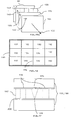
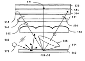
- the input illumination structure of the system is illustrated in fig.7.
- An array of birefringent microlenses 102 with director direction 104 is positioned over a liquid crystal layer 106 and an array of reflective pixels 108 comprising red data pixels 110, green data pixels 112 and blue data pixels 114.
- the display is illuminated from a first direction 116 for the red pixels, a second direction 118 for the green pixels and a third direction120 for the blue pixels.
- the illumination polarisation direction 124 is parallel to the extraordinary index 104 of the lenses which are immersed in an isotropic material 126.
- the illumination of a single colour pixel in JP11271744A is shown in fig.8.
- An input illumination cone substantially co-directional with input ray 118 with a polarisation state 124 is focussed by the lens 102 on to the pixel 112.
- Light is modulated by the LC layer 106 and reflected by the pixel 112 so that it has a component of polarisation 128 orthogonal to the input polarisation state 124.
- Output rays 130 are produced which are collected by a fixed beam-splitting component (not shown) and a projection lens (not shown) and directed towards a projection screen (not shown).
- An LCD panel with an array of birefringent microlenses is illuminated by separate linear polarised cones of red, green and blue light.
- the material surrounding the birefringent lenses has a refractive index substantially the same as the slow axis of the birefringent material.
- the fast axis of the birefringence of the material in the lenses is arranged so that the lens is analysed by the input linear polarisation.
- the green light is sent to the green pixel, red to red and blue to blue by the action of the lens.
- the useful light to be sent to the projection screen is in the orthogonal polarisation state. This output polarisation state sees the index matched slow axis of the birefringent microlens and thus no lens is analysed.
- the output of the display is not vignetted by the aperture of the microlenses, and the full cone of light from the device can be collected by the projection lens.
- Such a device can illuminate and collect the light efficiently from a single reflective LCD panel, to produce a low cost and bright projection system.
- Such a device is not used for a directional display system, nor is the effect of the birefringent lens switchable.
- Directional displays in which a different image is viewed from a different direction to enable an interactive image visualisation experience are well known in the art.
- printed lenticular screens are used to show two different advertising images in different directions.
- a reflective layer is placed behind a transmissive display. Ambient light falling on the display is reflected by the reflective layer back through the display towards an observer.
- Such displays suffer from loss of brightness from having two passes through the display and inefficient diffusion from the reflective layer.
- a transmissive display In a second class of display (backlit transmissive display operating in reflection), also known as a type of transflective display, the reflective layer at the rear of a transmissive display has an additional light source and light guide such as one or more light emitting diodes or fluorescent tubes. In dimly lit environments, the light source is switched on to increase the brightness of the display. The use of a light source will increase the power consumption of the display.
- additional light source and light guide such as one or more light emitting diodes or fluorescent tubes.
- a third class of display is described for example in "Influence of rough surface upon optical characteristics of reflective LCD with a polariser", Y. Itoh et al, pp. 221-224, SID Digest 1998.
- a reflective layer is incorporated within the structure of the display, substantially at the pixel plane.
- the reflector may comprise a rough surface so as to provide diffusion of the incident light.
- a diffuser may be incorporated on the front surface of the display. Holes may be provided in the reflector so as to provide for transmission of light from a backlight to provide a type of transflective display.
- a front-light may be provided to allow illumination from an auxiliary light source positioned at the front of the panel.
- Such a display provides increased efficiency of use of ambient light sources, and so is particularly suitable for use in colour reflective displays where increased light losses are associated with the colour filters.
- a volume reflection hologram is positioned at the rear of a reflective display which directs incident light in a separate direction to the direction of the specular reflection.
- three separate holographic elements are provided within the LCD, which gives a complicated and expensive structure.
- a focussing and colour splitting hologram element is also shown for a projection system. The hologram serves to focus an off-axis incident white light source separately for red, green and blue pixels.
- a plane reflective element reflects the light back towards a projection lens, with the holographic lens having no substantial effect on the reflected light. Such a display works for a narrow range of illumination angles and is therefore not suitable for use in a direct view system.
- a light direction switching apparatus for use in a directional display apparatus, comprising the following elements suitable for arrangement in series with a spatial light modulator:
- a method of directionally switching light in a directional display apparatus comprising:
- a directional display apparatus comprising:
- the present invention provides, inter-alia, an optical switching mechanism comprising at least one passive birefringent lens element and at least one separate polarisation modifying element that can be switched between directional and non-directional modes for providing one of:
- This invention enables the generation of autostereoscopic 3D images and full resolution 2D images of high quality with low levels of image cross talk and high brightness.
- This invention also enables the generation of a directional multi-viewer display that can be switched between a 2D mode and a mode in which images (which may be different) can be seen by different viewers from a wide range of directions.
- the function of the lenses can be adjusted by controlling the output polarisation of the device.
- the alignment condition in a passive element need only be maintained during the fabrication process whereas electrically switchable birefringent microlenses of the prior art must maintain the integrity of the alignment throughout the display lifetime and range of operating conditions.
- This invention enables the use of cured liquid crystal polymer type materials in the birefringent microlenses. This enables the birefringent properties of the birefringent material to be substantially fixed at the time of manufacture.
- Variations in liquid crystal birefringence with temperature for nematic phase liquid crystal materials as required in prior art switchable microlens devices means that the optical performance of electrically switched lenses will vary with temperature. This means that the optical quality of the generated windows will also vary with temperature. Therefore, as the temperature of operation of the prior art device varies in the electrically switchable microlens devices, the performance of the mode in which an index matching condition is required (2D mode), and the mode in which high performance windows are required (3D mode), will vary. This will cause the prior art display to operate away from its optimum operating conditions as the temperature is varied.
- the solid polymer material which can be used will maintain optimum operating conditions over a wider operating temperature range than the nematic phase (uncured) materials needed for electrically switchable lenses. This would be particularly important in environmentally demanding applications, for example automotive applications.
- the microlenses By arranging the microlenses to be internal to the glass substrate, reflections from the surfaces of the lenses can be minimised and the output surface (which may be planar) can be broadband anti-reflection coated.
- the switching rotation function polarisation modifying device (such as a half waveplate) may be manually re-configurable which minimises the additional cost and complexity of the system.
- a single SLM & birefringent microlens combination can be used for products with either mechanically switched or electrically switched properties, thus reducing the inventory.
- the final product configuration is determined by the choice of subsequently attached polarisation modification device component.
- a further advantage of the structure for electrically switching compared to the prior art, is that the active element may be fabricated by commercially proven techniques.
- the thin flat substrates mean that low voltages may be used.
- Standard liquid crystal spacing techniques may also be used. This is not the case as for thicker liquid crystal layers as are used for example to cover the microlens form factor.
- the electronically switchable waveplate of the present invention may be configured from a nematic liquid crystal or bistable device such as a ferroelectric liquid crystal and thus require no additional power consumption other than when switching between modes.
- the switching element may be segmented to allow 2D and 3D zones of the same brightness simultaneously on the display.
- the technology may be applied to a wide range of spatial light modulators including transmissive, reflective and transflective liquid crystal displays and emissive displays.
- Such a display requires a relatively low precision alignment of a polariser to the output compared to the high precision alignment of the parallax optic with respect to the display.
- the high precision alignment is fixed during the manufacture of the display while the low precision alignment is made manually for which only one degree of freedom of alignment is necessary. Therefore the physical mechanism by which the user reconfigures the display is less complex and costly than the case where the parallax optic is attached and detached to the display surface for the conversion between 2D and 3D modes of operation.
- lenticular lenses within the substrate means that the Fresnel reflections from the lens surfaces are substantially reduced compared to the element in air. This means that the element has a lower level of scatter and that anti-reflection coatings may be conveniently applied to the plane outer surface of the device. In addition reflections from a high refractive index Indium Tin Oxide (ITO) layer are not present (as would be the case with electrically switched lenses), so the visibility of the element itself in the display will be reduced.
- ITO Indium Tin Oxide
- a sweet spot indicator can be configured to have substantially the same optical performance as the display, but does not need to use any of the display area. Such a display is thus particularly suitable for handheld displays in which the area of the display is limited.
- the viewing freedom of the display can be enhanced by addition of an observer tracking function which can be implemented by moving the birefringent microlens in synchronisation with the measured position of a moving observer; or adjusting the image presented in correspondence with the measured position of an observer.
- an observer tracking function which can be implemented by moving the birefringent microlens in synchronisation with the measured position of a moving observer; or adjusting the image presented in correspondence with the measured position of an observer.
- a high brightness transflective or reflective display advantageously has a first mode with substantially non-directional properties as defined by the reflector material of the display and in a second mode has directional brightness property such that the display brightness is greater from a defined range of angles.
- Such a display works in full colour and can be used to increase the brightness of both reflective and transmissive modes of operation. Switching between the modes may be accomplished by means of a electrically switchable polarisation rotator.
- a multi-viewer display can be configured so that in one mode of operation all viewers can see the same image and in a second mode of operation different viewers can see different images to allow multiple simultaneous uses of the display.
- Such a display may be particularly suitable for systems such as automobile displays, automatic teller machines and seat-back aviation entertainment displays.
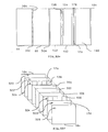
- Fig.9a shows a light direction switching apparatus (or light directional distribution switching apparatus) of a first exemplary embodiment of the invention.
- the light direction switching apparatus comprises a passive birefringent microlens and a switchable or variable polarisation modifying device 146 (which may also be termed a polariser) as shown in fig.9a.
- the birefringent microlens is provided by a lens substrate 132 having an isotropic material 134 deposited upon it on which is formed a microstructured surface 136.
- a birefringent material 138 with a defined birefringent optical axis direction 140 defining the direction of the extraordinary index, or director of the birefringent material is placed on the microstructured surface 136.
- a microlens counter substrate 142 with a plane surface 144 is positioned parallel to the lens substrate 132 to form a sandwich of the birefringent material 138.
- the switchable polarisation modifying device 146 is positioned to one side of the passive birefringent microlens device.
- the embodiment of Fig.9a represents a simple embodiment of the invention.
- the apparatus may be used in any application requiring switching of light between two directional distributions.
- One particularly desirable application is to use the apparatus in conjunction with or as part of a display device, such as a liquid crystal display device.
- many of the embodiments described below are of light direction switching apparatus in conjunction with or forming part of such display devices.
- the many preferred features of the light direction switching apparatus described in the context of the display device embodiments below may also be applied, singly or in any combination, to light direction switching apparatus of the present invention, for example such as that shown in Fig.9a, for use in display devices other than liquid crystal display devices, and indeed for use in or as used with devices and applications other than display devices or display applications.
- the preferred features may be implemented in such other devices or applications either directly, analogously or equivalently, in dependence upon the structures or modes of operation of those devices or applications.
- Fig.9a Operation of the apparatus shown in Fig.9a will be described below in relation to its use in a variety of displays, especially switchable 2D-3D displays, and other applications.
- the apparatus when implementing the apparatus of Fig. 9a in the majority of practical applications for it, including the display application embodiments below, it is appropriate to arrange the apparatus such that input light passes through the birefringent microlens before reaching the polarisation modifying device 146 (in which case the polarisation modifying device 146 acts as a polarisation analyser with respect to the light that has passed through the birefringent lens).
- the birefringent lens can be placed close to light modulating elements, e.g. pixels, of a display device.
- the apparatus shown in Fig. 9a may be arranged or used such that the light passes either way through it, i.e. so as to pass through the birefringent microlens before the polarisation modifying device, or so as to pass through the polarisation modifying device before the birefringent microlens, and that this is also the case for the other embodiments described below.
- the apparatus of fig.9a may be arranged so that when illuminated by light of one polarisation component, the lenses operate to form a real image of an object.
- the object may be for example a light source which may be placed close to the lenses.
- the light source may be for example pixels of a display device.
- a real image must lie on the opposite side of the lens to the object.
- the real image may be positioned at a window plane.
- the window plane may be substantially planar although as well known in the art will be distorted by aberrations due to the imaging properties of the lenses.
- the lenses may have a different optical function and so a real image is not formed at the window plane.
- the lenses can be configured to have substantially no optical power so that there is substantially no modification of the light rays from the light sources. In this case, the object and image will lie in substantially the same plane on the same side of the lenses. Thus the lenses do not operate to form a real image of the object in this polarisation mode.
- Such a configuration will advantageously allow the switching of the optical property of the lenses to allow the formation of viewing windows in a first mode and no viewing windows in a second mode.
- Such an apparatus can advantageously be used for example in switchable 2D to 3D displays using the binocular parallax effect in which a spatial light modulator comprising an array of pixels is placed at the object plane of the lenses.
- the lenses In the first (autostereoscopic 3D) polarisation mode the lenses form a real image of the display pixels substantially at the window plane which is on the opposite side of the lenses to the display pixels. Each eye of an observer positioned substantially at the window plane will see one of a stereo image pair comprising a planar image at the lens optical apertures.
- the lenses are arranged to have substantially no optical power and thus the image of the object is substantially at the plane of the object. Thus the image is not a real image as it is on the same side of the lens.
- the same planar image may be seen by both eyes of the observer at the plane of the display pixels at the object plane.
- the observer sees the full pixel resolution of the spatial light modulator.
- Such an apparatus can also be advantageously used for example in switchable high brightness reflective displays in which a spatial light modulator comprising an array of pixels is placed at the object plane of the lenses.
- a spatial light modulator comprising an array of pixels is placed at the object plane of the lenses.
- the lenses image the object to a real window plane on the opposite side of the lenses.
- An observer positioned at the window plane may see an enhanced brightness image for an appropriately positioned external light source.
- the image is substantially on the same side of the lens as the object plane, and no brightness enhancement can be seen.
- the apparatus may be adapted so that the switchable polariser may be arranged to switch a planar image such as for example in a 2D to 3D switching apparatus or a switchable reflective display brightness enhancement apparatus.
- the observer will see the planar image substantially at the plane of the aperture of the lenses of the display device in a first polarisation mode or at the plane of the pixels of the display device in a second polarisation mode.
- the image here does not refer to the real image of the pixels at the window plane in the first polarisation mode.
- the switchable polariser may be uniformly switched such that adjacent lenses are operating in the same polarisation mode. This allows regions of the displayed image to be seen in the same mode of operation. This advantageously reduces the complexity and cost of the switchable polariser. Additionally, there is no constraint on the separation of the lens array and switchable polariser. There is no parallax between the lens array and switchable polariser over the uniform area.
- Fig.9b shows an embodiment where a light direction switching apparatus is used in or incorporated with a switchable 2D-3D display device.
- a directional distribution switching device of the type shown in Fig.9a is attached to the front surface of an LCD.
- a backlight 60 produces a light output 62 which is incident on an LCD input polariser 64.
- the light is transmitted through a TFT LCD substrate 66 and is incident on a repeating array of pixels arranged in columns and rows in an LCD pixel plane 67.
- the red pixels 68,71,74, green pixels 69,72,75 and blue pixels 70,73 each comprise an individually controllable liquid crystal layer and are separated by regions of an opaque mask called a black mask 76.
- Each pixel comprises a transmissive region, or pixel aperture 78.
- the pixel Light passing through the pixel is modulated in phase by the liquid crystal material in the LCD pixel plane 67 and in colour by a colour filter positioned on an LCD colour filter substrate 80.
- the light then passes through an output polariser 82 and through the microlens counter (carrier) substrate 142, birefringent microlenses 138 with birefringent optical axis direction 140, isotropic microstructured material 134 and lens substrate 132.
- a polarisation modifying device 146 is added.
- the birefringent microlens is configured as a cylindrical lens array. Each lens extends across the entire display in one direction and the lenses repeat across the display in the perpendicular direction.
- the combination of backlight 60, LCD 64,66,67,80,82 and birefringent microlens structure 142,138,134,132 is grouped together to form the display 148.
- the direction of the director of the LC is shown in fig.9a and subsequent figures. This shows the direction of the extraordinary component of the birefringence of the birefringent material.
- the birefringent microlens is sandwiched between the output polariser of the display and an analysing polariser.
- the direction of the optical axis of the birefringent material (the director direction, or the extraordinary axis direction) will be referred to as the birefringent optical axis. This should not be confused with the optical axis of the lenses which is defined in the usual way by geometric optics.
- a backlight illuminates the rear of the display.
- a polariser analyses the light from the backlight which is then incident on the pixels of the LCD.
- An LCD is a class of phase modulating spatial light modulator (SLM) and uses polarisers to convert the phase modulation to an intensity modulation which analyse the output polarisation of the pixels.
- SLM spatial light modulator
- the phase of the incident light is modulated according to the voltage across the pixel, which for a thin film transistor twisted nematic (TFT-TN) type LCD of this particular embodiment is controlled using an array of matrix addressed transistors on the active substrate of the device.
- the output is then transmitted through an array of colour filters placed on the counter substrate of the LCD or directly on the active substrate.
- a black mask is used to shield the addressing electronics and to produce well defined pixel apertures.
- This light is then analysed by the LCD's output polariser.
- the output light is then incident on an array of birefringent microlenses and the following analysing polariser 146.
- each pixel of the display is seen by the observer to be substantially at the aperture of the lens array, in a two dimensional plane in space.
- This display uses the binocular parallax effect on a planar display device and advantageously allows the display of opaque images. This applies to all embodiments in which the lens has optical power to be described below.
- Fig. 10a shows in expanded form the propagation of light from the LCD output polariser to the observer in a 3D mode of operation.
- the LCD output polariser 82 has a direction 149 of maximum transmission at 45 degrees to the vertical;
- the birefringent microlenses 138 have a direction of the birefringent material optical axis 140 at 0 degrees;
- the polarising modifying device 146 comprises a linear polariser, acting as an analysing polariser, with a direction 151 of maximum transmission of 0 degrees.
- the light is directed to the observer along the direction 150.
- Fig.10b shows in expanded form the propagation of light from the LCD output polariser to the observer in a 2D mode of operation.
- the LCD output polariser 82 has a direction 149 of maximum transmission at 45 degrees to the vertical;
- the birefringent microlenses 138 have a direction of the birefringent material optical axis 140 at 0 degrees;
- the polarising modifying device 146 i.e. linear polariser acting as an analysing polariser
- the light is directed to the observer along the direction 152.
- Fig.10 shows the method of operation of the birefringent microlenses in the 3D and 2D modes.
- the microlenses formed from a combination of the microstructure and the birefringent material in this case are lenticules, that is they are cylindrical lenses with a vertical axis of symmetry. Such an arrangement can provide horizontal parallax only, which is sufficient for many autostereoscopic applications due to the generally horizontal separation of the viewer's eyes.
- This invention can also be applied to two dimensional arrays of lenses.
- the output polarisation direction for light from transmissive TFT TN-LCDs is generally set at or near to 45 degrees to the vertical.
- the light incident on the microlenses in fig.10a can be resolved in to vertical and horizontal linear polarisations.
- the vertical polarisation state sees the extraordinary axis of the birefringent material and the polymer index. As these indices are different, the curvature of the lens has an optical effect and the lens function is present.
- the lenticules then generate the windows in the viewing space, as described in fig.6.
- the directional distribution is the 3D directional distribution.
- the resolved output linear polarisation state from the LCD sees the ordinary index of the birefringent material. As this is index matched to the polymer material, then no index change is seen at the interface, and the lens has no function in this polarisation state.
- an output polariser is positioned whose transmission axis is horizontal as shown in fig. 10b, the output light which is provided is that component of the light that has not been substantially modified by the microlens array and thus no windows will be generated and the display will appear to be a full resolution 2D display with substantially no modification to the directional distribution of the base panel.
- the invention is not limited to the transmissive mode of operation of the device.
- the display device may employ any type of spatial light modulator to modulate the light output by each pixel, including transmissive, emissive or reflective, or even a combination thereof.
- the display can be configured with a mirror as part of the backlight structure, so that light incident through the front of the display is reflected back through the display to the observer.
- the invention is not limited to the TFT TN-LCD effect.
- Other effects including, but not limited to In-Plane-Switching (IPS), vertically aligned (VA), Advanced Super View (ASV), and emissive displays such as electroluminescent, organic electroluminescent, plasma, plasma addressed liquid crystal, vacuum fluorescent may be used.
- IPS In-Plane-Switching
- VA vertically aligned
- ASV Advanced Super View
- emissive displays such as electroluminescent, organic electroluminescent, plasma, plasma addressed liquid crystal, vacuum fluorescent may be used.
- Polarisation modifying device 146 i.e. switchable polariser
- the switchable polariser i.e. the polarisation modifying device 146
- displays are rectangular, substantially rectangular, or some other shape with an aspect ratio other than 1:1.
- the polariser cannot be made to match the display shape if it is to also be moveable between the two switchable positions described above.
- This problem is addressed by further embodiments described below which provide arrangements whereby the polarisation modifying device requires to be repositioned in a way that preserves the positioning of the area of the polarisation modifying device 146 with respect to the shape of the display.
- the polarisation modifying device 146 is implemented in an electrically switchable form.
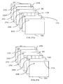
- Fig. 11 shows one configuration of a polariser stack that could be used for the polarisation modifying device 146.
- Fig.11a shows a plan view of the device.
- a substrate 156 has a polariser 158 attached on one side and a half waveplate 160 attached on the other.
- Fig.11b shows schematically the orientation of the axes of the components in the device.
- the polariser 158 has an axis of maximum transmission 162 at 0 degrees to the vertical, while the half waveplate 160 has an effective birefringent optical axis direction 164 at 45 degrees to the vertical.
- the polariser stack comprises a linear polariser whose transmission axis is positioned vertically, a mounting substrate, that could be a non-birefringent plastic for example and 90 degree polarisation rotating element which could be for example a broadband half waveplate whose birefringent optical axis is positioned at 45 degrees to the vertical.
- the waveplate serves to rotate a linear polarisation through twice the angle of the incident polarisation to the birefringent optical axis direction.
- the half waveplate thus has a 90 degree polarisation rotation function.
- the half waveplate can be replaced by another type of 90 degree polarisation rotating element such as a twisted nematic cell.
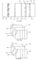
- Fig.12a shows the configuration of the display in the 3D mode.
- the LCD output polariser 82 has a transmission axis 149 of 45 degrees (to the vertical) and is followed by the birefringent microlenses 138 which have an optical axis direction 140 at 0 degrees to the vertical, which is followed by the half waveplate 160 with a birefringent optical axis direction 164 of 45 degrees and a polariser 158 with a maximum transmission axis direction 162 of 90 degrees to the vertical.
- the 3D output directional distribution 150 is towards the observer (not shown).
- Fig.12b shows the configuration of the display in the 2D mode.
- the LCD output polariser 82 has a transmission axis 148 of 45 degrees and is followed by the birefringent microlenses 138 which have an optical axis direction 140, which is followed by the polariser 158 with a maximum transmission axis direction 162 of 90 degrees to the vertical and subsequently by the half waveplate 160 with a birefringent optical axis direction 164 of -45 degrees.
- the 2D output directional distribution 154 is towards the observer (not shown).
- Fig.12a shows the use of the polariser stack in the configuration equivalent to fig.10a.
- the 3D output from the display is in the vertical polarisation, the half waveplate rotates this polarisation to the horizontal and the output polariser transmits this polarisation state.
- the 2D output which is horizontal from the LCD, is rotated to vertical by the half waveplate and is extinguished by the output analysing polariser.
- Fig.12b shows the polariser configuration for the 2D mode in which the analysing polariser stack is removed from the display, rotated about a horizontal or vertical axis and placed back on to the front of the display.
- the analysing polariser 162 then extinguishes the vertically polarised light from the birefringent microlens 138 which sees a lens function and transmits the horizontally polarised light which does not see a lens function.
- the output polarisation is then incident on the half waveplate, but as there is no subsequent polariser, this has no useful function on the display output.
- the display has a full resolution 2D image.
- the orientation of the half waveplate and polariser in figs 11 and 12 may be reversed so that the half waveplate is used in the 2D mode rather than the 3D mode and vice versa.
- the optimum choice is made by considering the spectral polarisation properties of the half waveplate. Multiple stack half waveplates may be used to improve performance in both orientations.
- the output polarisation of the LCD is defined to be 45 degrees.
- the invention is not limited to this and the angle may be arbitrarily set in the optimum design of the unmodified display. The angles of the components in the remainder of the system are adjusted accordingly.
- the birefringent optical axis may no longer be aligned parallel to the elongate axis of the lenticules.
- the birefringent optical axis is set relative to the output polarisation of the LCD such that the input polarisation is analysed in to the two orthogonal components.
- Figs.13 and 14 show alternative representation of the propagation of polarised light through the stacks for 2D and 3D modes respectively.
- the directional display 148 is followed by the polarisation modifying device 146 which comprises a polariser 158, substrate 156 and half waveplate 160.
- the light is shown as propagating along the direction 166.
- the output polariser 82 the light 168 is polarised at 45 degrees.
- the birefringent lens 138 the light can be resolved in to two components.
- the vertical component 170 sees the lens function and therefore contains the directionality information for the 3D mode.
- the horizontal component 172 does not see the lens function and thus contains the directionality information for the 2D mode.
- the polariser 158 extinguishes the vertical polarisation state 170 and allows the horizontal polarisation state 172 to pass.
- the output waveplate 160 will modify the phase of the output polarisation state, but as human vision is not polarisation sensitive, no effect will be seen by the user of the waveplate 160, giving a 2D output with the corresponding 2D directional distribution.
- the directional display 148 is followed by the polarisation modifying device 146 which comprises a polariser 158, substrate 156 and half waveplate 160.
- the light is shown as propagating along the direction 166.
- the output polariser the light 168 is polarised at 45 degrees.
- the birefringent lens 138 the light can be resolved in to two components.
- the vertical component 170 sees the lens function and therefore contains the directionality information for the 3D mode.
- the horizontal component 172 does not see the lens function and thus contains the directionality information for the 2D mode.
- the waveplate 160 rotates the vertical polarisation 170 to horizontal and the horizontal polarisation 172 to vertical.
- the polariser 158 extinguishes the vertical polarisation state 172 and allows the horizontal polarisation state 170 to pass giving a 3D output.
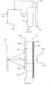
- Fig.15a shows the directional display 148, followed by another form of implementation of the polarisation modifying device 146, comprising a switchable waveplate 176 and a linear polariser 184.
- the switchable waveplate 176 is sandwiched between a pair of transparent electrodes 178 which are attached to the display 148 and to an electrode substrate 180.
- An optional waveplate (or film) 182 to provide correction (which may be Pancharatnum correction) of polarisation rotation is attached to the electrode substrate 180; and the linear polariser 184 is attached to the optional waveplate (or film) 182. This may advantageously increase the viewing angle of the display.
- the propagation of light through the system for the 3D mode is also shown.
- the light is shown as propagating along the direction 166.
- the light 168 is polarised at 45 degrees.
- the birefringent lens 138 the light can be resolved in to two components.
- the vertical component 170 sees the lens function and therefore contains the directionality information (or directional distribution) for the 3D mode.
- the horizontal component 172 does not see the lens function and thus contains the directionality information (or directional distribution) for the 2D mode.
- the optical axis of the switchable waveplate 176 is aligned parallel to the-horizontal input polarisation, and therefore imparts no rotation on the polarisation states outputted from the birefringent microlenses.
- the optional waveplate 182 function serves to improve the chromatic and viewing angle performance of the waveplate, and its function is well known in the art so will not be described here.
- the horizontal polarisation state (carrying 2D directionality information) is then transmitted through the output polariser.
- the switchable waveplate 176 is electrically controlled such that its optical axis is at 45 degrees to the vertical.
- the switchable waveplate 160 rotates the vertical polarisation 170 to horizontal and the horizontal polarisation 172 to vertical.
- the polariser 184 extinguishes the vertical polarisation state 172 and allows the horizontal polarisation state 170 to pass giving a 3D output.
- Fig.15b shows schematically the propagation of light from the LCD output polariser 82 through the birefringent lenses 138, switchable waveplate 176 and output analysing polariser 184.
- the electrodes and optional waveplate are removed for convenience of description.
- the half waveplate 176 has a 45-degree birefringent optical axis direction 164.
- the half waveplate 180 has a 90-degree birefringent optical axis direction 164.
- the mechanically switched element has been replaced by an electronically switched 90-degree rotation function such as a liquid crystal layer positioned between transparent electrodes (such as Indium Tin Oxide, ITO).
- an electric field is applied across the device such that it optical axis is in one direction.
- the field is changed or removed and the optical axis of the device is changed to a different orientation.
- the 90 degree rotation function may be a switchable half waveplate, for example a Ferro-Electric LC cell or nematic electrically controlled birefringence cell.
- the device may be a guided mode device, such as a TN cell. Such devices are well known in the art.
- this active device may be combined with passive waveplate components such as appropriately oriented half waveplates as for a 'Pancharatnam' configuration.
- passive waveplate components such as appropriately oriented half waveplates as for a 'Pancharatnam' configuration.
- Combinations of waveplates for broadband performance are disclosed for example in Proc. Ind. Acad. Sci. vol41 No.4, section A, pp130, S. Pancharatnam “Achromatic Combinations of Birefringent Plates", 1955.
- the 90 degree rotation device operates as a half waveplate.
- the switchable waveplate extraordinary axis orientation is 0 or 45 degrees.
- the switchable waveplate orientation may be for example +/-22.5 degrees and the passive waveplate may be for example 67.5 degrees.
- the birefringent lenses themselves comprise for example a liquid crystal material sandwiched between a microstructure and a plane substrate with electrodes placed on each surface.
- these lenses show poor optical quality in both modes (such as disclinations of the liquid crystal material), and require deposition of complex electrode structures on the microstructured surface.
- These lenses will also exhibit temperature dependent performance due to the variation of birefringence of the liquid crystal material indices with temperature.
- These lenses will also produce diffuse frontal scatter effects due to reflection of light from the curved lens surfaces which are coated in partially reflective electrode material such as ITO. The diffuse scatter will serve to degrade the contrast of the display when used in brightly lit environments.
- the apparatus comprises a separate polarisation sensitive imaging element and an active polarisation switching element.
- a standard commercially proven thin-cell switching element can be used which has a low level of complexity and cost to manufacture which alleviates the problems associated with switching the lenses directly.
- Such a device can also operate over a wide temperature range and has reduced scatter due to reflections from the curved lens surface. It can also use standard cell spacing techniques. It does not need to take account of different electric field strength as a consequence of the physical relief of the microstructure.
- the passive birefringent microlens is also simpler to manufacture and does not need to be compatible with electronic driving schemes using electrode layers.
- the refractive index properties of the birefringent material can be substantially set during curing if a cured LC material is used. This means that as the temperature of operation varies, the index of the substrate and LC material will be maintained substantially the same.
- a change in the refractive index of the material will occur with temperature. This will result in a variation of the property of the lens with temperature, which relies on index matching to achieve a 2D mode, and a defined focal length to achieve a 3D mode.
- the regime of operation of the lens in 2D and 3D modes may be limited compared to the present invention.
- a further advantage of the separate switched 90 degree rotator element of this embodiment is that it can be conveniently manufactured using proven LC cell spacing techniques when compared to spacing the LC cell when one substrate is highly structured (e.g. a microlens).
- the electrical contacts on the microstructure surface may make the cell more likely to make unwanted electrical contact across the cell.
- the attachment of the electrode layer may be less robust on the curved surface making it more prone to electrode flaking.
- the variation in electric field strength may need to be accounted for which may make the device thicker. Fabrication of segmented elements is more difficult on a microstructured surface. This makes the fabrication of segmented elements more feasible.
- Fig.16 shows a segmented active polarisation rotation switching element.
- the total display area 190 can be divided in to sections in which the polarisation rotation can be either 0 degrees or 90 degrees.
- the display can comprise regions 192 of full resolution 2D images and regions 194 of directional 3D images. This may be useful for adding 2D text around a 3D image for example. In the display of the present invention, these regions will have substantially equal brightness which is a particular advantage of this invention.
- the sections are provided by segmented electrodes, with gaps therebetween. This segmented approach may be applied to other electrically switched forms of the polarisation modifying device 146.
- Fig.17 shows a detail in cross section of the display of fig.16 in the region of a gap 196 between two segmented 198 electrodes on one substrate.
- a uniform transparent electrode 200 is provided on the opposite substrate.
- a gap 196 is formed between the two segmented electrodes 198 to prevent conduction between the two segmented portions.
- Electric field lines 197 are marked.
- a distorted field region of liquid crystal switching material is formed in the region 199 of the gap between the segmented electrodes.
- Fig.17 further shows the effect-of the gap 196 on the device performance (i.e. it forms a distorted field region 199).
- the output of the display is desirably uniform, particularly in the 3D mode. If the gaps between the segmented electrodes are visible, they will appear as a grid of lines in the plane of the display surface and will result in a visually disturbing artefact in the final image. This is because the gaps would appear to be as a 2D plane artefact interrupting the 3D depth planes and result in visual strain. In a further embodiment this effect is alleviated by orienting the alignment layers and switching of the device such that in the 3D mode, the gaps have the same alignment of the switching material as the electrodes.
- the gaps may be made to be sufficiently small that the fringing field of the electrodes means that the material is switched across the gap.
- Such performance can be improved by using a material with a sharp threshold between switched states, such as binary switch state materials (such as ferroelectric liquid crystals).
- binary switch state materials such as ferroelectric liquid crystals.
- the number of segments can be increased, to increase the fiexibility of the positioning of the 3D window in a 2D background.
- Fig.18a shows a detail of the construction of one birefringent microlens structure.
- the LCD counter substrate 80 is followed by the output polariser 82 and the microlens counter substrate 142.
- An alignment layer 202 is formed on the microlens counter substrate 142 and a second alignment layer 204 on a isotropic lens microstructure 134 which is in turn attached to a lens substrate 132.
- a birefringent material with a director alignment direction 140 is sandwiched between the alignment layers 202,204 and takes on the alignment of the alignment layers.
- the LCD counter substrate has a polariser (and possibly view-angle correction films well known in the art) attached to its outer surface.
- the birefringent microlens stack is attached to this surface.
- the stack comprises a microlens counter substrate with a liquid crystal alignment layer attached to one side.
- the birefringent microlenses comprise an array of lenses in which at least one of the lens forming materials is birefringent with a birefringent optical axis direction that is fixed for all the lenses.
- the lens may be a convex birefringent lens formed by filling the gap between a plane substrate and a concave moulded polymer substrate.
- the birefringent material can be for example a liquid crystal material which fills the gap and is aligned by means of alignment layers attached to, or on each of the substrates.
- microstructured surface may be embodied for example as structures including individually or in combination cylindrical microlenses, circular microlenses, off-axis lenses, prisms or diffractive structures.
- the refractive index and dispersion of the polymer is set to be substantially the same as at least one refractive indicia (e.g. the ordinary component of refractive index) and/or dispersion for the birefringent material.
- the polymer and substrate material are substantially non-birefringent. (Thus, in the switched clear state, there is only low visibility of the lens structure).
- the birefringent lenses can be formed by:
- the fill may take place at an elevated temperature.
- the cell may need to be sealed using conventional techniques, for example thermo-setting sealant.
- the birefringent material may be cured in a polymer network. The curing may be by known means for example UV light.
- the birefringent material may be a cured liquid crystal polymer material such as are commercially available, for example RM257 from Merck Ltd..
- fixed polymer network With a fixed polymer network, the alignment condition need only be correct at the time of manufacture. Also, fixed polymer network material has less variation of refractive indices, with temperature than an uncured liquid crystal material.
- the processes for mastering the replicated polymer microstructure for example by laser scanning of photoresist, diamond ruling, photoresist patterning and reflow
- replicating optical microstructures for example by means of hot embossing, injection moulding or UV embossing
- the residual birefringence of this material should be minimised to avoid polarisation cross talk in the output of the microlens stack. Polarisation cross talk would result in mixing of 3D and 2D modes when an output analysing polariser is applied.
- the alignment layer may be attached to or formed on the plane and replicated microstructured surface by means of for example spin coating, roll coating, spray coating or evaporated coatings.
- Each of the alignment layers can be rubbed using standard rubbing techniques well known in the art to produce homogeneous (planar) alignment in which the liquid crystal molecules align substantially parallel to the surface, with a small pretilt to remove degeneracy.
- the alignment layers can be homogeneous rubbed alignment layers such as spun polyimide, rubbed anti-parallel to the long axis of the microlenses.
- An alignment layer direction and pretilt properties may also be produced using photo-alignment layers with suitable exposure to polarised and unpolarised light as well known in the art.
- the microlens counter substrate alignment layer 202 has an alignment direction 206 and the microlens substrate alignment layer 204 has an alignment direction 208 which is anti-parallel to 206.
- the anti-parallel alignment gives a substantially uniform pretilt through the thickness of the cell structure.
- the orientation of the rub direction will depend on the output polarisation of the LCD, whereas the orientation of the geometric microlens axis is set to be vertical.
- a cylindrical lens describes a lens in which an edge (which has a radius of curvature) is swept in a first linear direction
- the geometric microlens axis is defined as the line along the centre of the lens in the first linear direction, ie parallel to the direction of sweep of the edge.
- the geometric microlens axis is vertical, so that it is parallel to the columns of pixels of the display.
- the geometric microlens axis is horizontal so that it is parallel to the rows of the pixels of the display.
- figure 19c shows an arrangement for construction of the birefringent lens array.
- An alignment layer 202 on the microlens counter substrate 142 is arranged so that the orientation 207 of the birefringent optical axis of the liquid crystal material is at 45 degrees to the vertical.
- the alignment orientation 209 is set to be parallel to the lenses.
- the output polariser orientation is then at 0 degrees to the vertical for the 3D mode and 90 degrees for the 2D mode.
- the embodiment of fig.19c is particularly advantageous for construction of the lens cell.
- the commonly used output polarisation direction of well known TFT-LCD devices is set at 45 degrees to the vertical. In operation, this polarisation state should be incident on the ordinary or extraordinary optical axis of the birefringent microlens array.
- One configuration would be to attach or form an alignment layer to or on the microstructured surface which is parallel or anti-parallel to the direction of the output polarisation of the display i.e. at 45 degrees to the vertical. This will be in a different direction to the geometric microlens axis direction.
- the alignment of the liquid crystal material at the microstructured surface may be influenced by both the alignment layer formed on it and the microstructured surface itself.
- the microstructure itself may impart some preferred alignment properties to the liquid crystal material in the birefringent microlenses. This may cause undesirable artefacts in the birefringent microlens structure such as birefringent material dislcinations. Such artefacts may degrade the optical performance of the lens, for example through increased levels of scatter, increased image cross talk and reduced image contrast.
- the alignment layer orientation direction may be substantially parallel to the direction of the geometric microlens axis for cylindrical lenses or substantially parallel to the long axis of other types of asymmetric microstructures.
- the long axis may for example be defined by the direction of grooves in the microstructure.
- good alignment quality may additionally be easier to achieve by rubbing along the direction of the geometric microlens axis for cylindrical lenses or substantially parallel to the long axis of other types of asymmetric microstructures.
- a waveplate can be used to rotate the output polarisation from the display prior to the birefringent lens such that the polarisation direction of the light falling on to the microlens counter substrate is vertical, and the alignment direction at both substrates of the birefringent microlens is vertical.
- the disclinations will not occur and the display performance may be improved.
- incorporation of such an element will increase device cost and complexity of manufacture. Additional components between the lens and pixel planes will also increase the viewing distance of the display which is undesirable.
- the alignment direction 207at the microlens counter substrate alignment layer 202 is set parallel or perpendicular to the output polarisation direction from the LCD, while the alignment direction 209 at the microstructured surface alignment layer 204 is set parallel to the geometric microlens axis direction.
- the birefringent material thus undergoes a twist of substantially 45 degrees through the thickness of the lens cell.
- twist angles of substantially 135 degrees could be used.
- Such a twist may guide the polarisation direction of the light through the cell, such that the input polarisation to the cell may be at 45 degrees and the output polarisation direction at the microstructured surface at 0 degrees to the vertical. It may additionally be desirable to increase the thickness of the cell such that the optical guiding property in the lens cell takes place over the entire lens surface.
- microstructured surface alignment is parallel to the direction 209 of the alignment layer 204.
- Such an element advantageously reduces the cost and complexity of fabrication of a lens cell for use with conventional TFT-TN LCDs while optimising image quality.
- this invention is not limited to configurations in which the alignment direction 209 at the microstructured surface is set parallel to the axis of the lens array.
- the linear output polarisation state direction 211 from the output polariser 82 of a TFT-LCD is aligned parallel to the alignment direction 207 of the microlens counter substrate alignment layer 202.
- the microstructured surface alignment layer 204 has an alignment direction 213 which is anti-parallel to the direction 207, and is thus inclined at an angle to the geometric microlens axis of the lenses.
- the microlenses may be tilted at an angle slightly different from vertical in order to increase the effective viewing angle of the display by creating multiple overlapping windows at the viewing plane.
- the optical axis of the birefringent material at the microstructure surface may be made parallel to the grooves of the lenses, such that there is a twist in the lens cell.
- the output polariser modifying element is then oriented parallel or orthogonal to the birefringent optical axis of the material at the surface of the microstructure.
- the alignment of material in the lenses may be made independent of the axis of the microlenses.
- the alignment mechanism may be incorporated as a grooved microstructure such as a diffractive relief structure superimposed on the lens shaped microstructure of the microlenses such that it can be formed during manufacture of the replicated microstructure.
- a grooved microstructure such as a diffractive relief structure superimposed on the lens shaped microstructure of the microlenses such that it can be formed during manufacture of the replicated microstructure.
- microlens arrays are also known in the art, for example S.Traut, H.P.Herzig “Holographically recorded gratings on microlenses for a miniaturized spectrometer array", Opt.Eng. vol39 (1) 290-298 (January 2000). Such structures may be used for the alignment of the birefringent materials on the surface of the microlenses.
- the diffractive structure will ideally have a pitch of the wavelength of visible light or less to avoid diffractive artefacts in the final image.
- An alignment layer direction and pretilt properties may also be produced using photo-alignment layers with suitable exposure to polarised and unpolarised light as well known in the art.
- Fig.18a shows the use of two homogenous alignment layers (for example formed by rubbing). During manufacture it may be desirable to fit the optical element following completion of the fabrication of the panel, or following fabrication of the colour filters on the opposite side of the LCD counter substrate.
- the alignment layers may be parallel or anti-parallel in order to optimise the viewing angle performance of the element.
- Fig.18b shows the same structure as fig.18a, but this time with a homeotropic alignment layer 202 and a homogeneous alignment layer 204.
- the birefringent molecules 210 at the alignment layer 202 are aligned substantially perpendicular to the surface, while the birefringent molecules 212 at the alignment layer 204 are aligned substantially parallel to the surface.
- Fig.19b shows a schematic view of the alignment layer directions equivalent to fig.18b.
- the microlens counter substrate alignment layer 202 has a homeotropic alignment direction 214 while the microlens substrate alignment layer 204 has a homogeneous alignment direction 216.
- the alignment layer on the counter substrate could be replaced by a non-rubbed alignment layer such as a homeotropic alignment layer.
- the alignment of the liquid crystal is substantially vertical at the counter substrate.
- the replicated microstructure has a homogeneous alignment layer with a pretilt so that the liquid crystal molecules are aligned substantially parallel to the replicated surface.
- such an alignment technique may provide a similar optical performance to the device of fig.18a, with some variation of index profile across the lens surface expected. Care should be taken to ensure that the optical axis_remains substantially parallel to the desired output polarisation to avoid unwanted phase birefringence effects from the lenses causing disruption to the liquid crystal mode properties.
- Fig.18c shows the use of an electric field 218 to align the birefringent molecule birefringent optical axis direction 220. Alignment layers described in previous embodiments are omitted.
- Fig.18d shows the use of a combination of a homogeneous alignment layer 202 on the microlens counter substrate 142 and an electric field 218 to align the birefringent molecules.
- the alignment mechanism may be by means of an electric or magnetic field applied across the device prior and during at least part of the curing of the polymer network.
- one or both of the alignment layers may be optionally omitted as shown in fig.18c for no additional alignment layers and fig.18d for a single additional homogenous alignment layer positioned on the plane substrate as shown, or on the replicated microstructure.
- the electric and/or magnetic field may be applied by external electrodes to the structure which are not part of the final device. Note that the direction of the electric field is along rather than across the cell for a positive dielectric anisotropy material. For a negative dielectric anisotropy material, the field may be applied across the cell.
- Fig.20a shows the configuration for which the alignment layer 202 is placed directly on the output polariser 82 of the display.
- the microlens counter substrate 142 has effectively been removed.
- the alignment layers 202 and 204 may be formed or omitted as described previously. Such a configuration may advantageously reduce the viewing distance of the display.
- Fig.20b shows a configuration in which the orientation of the optical surface of the lens microstructure 134 is reversed.
- the isotropic polymer material 134 will have a refractive index matched to the higher of the ordinary and extraordinary indices of the liquid crystal material, generally the extraordinary index.
- Fig.21 shows another configuration in which positive lenses formed in the isotropic microstructure 134 (whose index matches the extraordinary index of the birefringent material 138) are placed on the polariser 82.
- Fig.22 shows the equivalent situation for negative polymer lenses formed in the isotropic microstructure 134 on the polariser surface 82 in which the index of the isotropic material is matched to the ordinary index of the birefringent material 138.
- the alignment layers may be photo-alignment layers or obliquely evaporated Silicon Oxide or other well known alignment layers
- the spacing between the lenses and the planar substrate can be used to set the separation of the two layers and subsequently filled with liquid crystal material. This removes the requirement to use an additional spacer material as required in many conventional LC cells.
- the lenses may be allowed to touch the planar substrate 222 or polariser 82.
- low temperature alignment layer materials may be used, for example from Nissan Chemical Industries, Ltd..
- the optical design of the lenticular birefringent lens may be implemented according to conventional design approaches and requirements for lenticular screens for 3D displays, which requirements are well known in the art.
- the embodiments described previously can be implemented on a range of emissive displays in addition to LCDs, for example an electroluminescent display or a plasma display.
- the output of the display requires a polariser to be fitted, followed by the birefringent microlens and the analysing polariser of the light direction switching apparatus.
- the emissive technology is intrinsically polarised, it may be possible to omit the polariser or use a high transmission efficiency clean-up polariser.
- the invention can also be applied to reflective and transflective displays such as liquid crystal displays.
- each of the 2D and 3D modes will only have a brightness which be nominally 50%, typically 40-45% of the brightness of the unmodified display.
- the nominal viewing distance of such a display is determined by the separation of the liquid crystal display layer and the parallax optical element.
- a 4.7" VGA stripe pixel configuration display (640x3 horizontal x480 vertical colour pixels) for example has a colour sub-pixel pitch in the lateral direction of 50 microns and height 150 microns.
- a typical 3D display is required with windows of size 65mm (equivalent to the nominal human interocular separation). In this case, the spacing between the pixel plane and the aperture of the parallax optic (with refractive index equal to 1.5) will give a viewing distance of 430mm if a 0.5mm thick counter substrate is used.
- the spacing between the pixel plane and the optical aperture of the birefringent microlenses must include the polariser thickness and the LCD counter substrate thickness.
- the LCD counter substrate will be required to be of thickness 0.3mm.
- Standard counter substrate thicknesses are 1.1mm and, 0.7mm with consideration of 0.5mm likely.
- the counter substrate glass would be too thin to use currently available mass production materials.
- thinner glass or suitable plastic substrates may become more economically available in the future.
- the birefringent microlens array is positioned within or as an addition to the counter substrate of the LCD, i.e. between the phase modulating layer (i.e. the liquid crystal layer) and a single analysing polariser.
- the roles of the output (analysing) polariser of the basic display and the output (analysing) polariser of the light direction switching apparatus are shared.
- Fig.23 shows one such further embodiment of a display comprising a backlight 60, producing light output 62 which is incident on an LCD input polariser 64, an LCD TFT substrate 66, an LCD pixel plane 67 comprising an array of pixels arranged in columns and rows followed by an LCD counter substrate 80, an array of birefringent lenses 138, followed by an isotropic lens microstructure 134 followed by a lens substrate 132.
- the previous items can be grouped as a directional display device 236. Following the directional display device 236, a polarisation modifying device 146 is positioned. Compared to the previously described 'two output polariser' embodiments, the LCD output polariser 82 is omitted.
- the polarisation modifying device 146 transmits horizontal linearly polarised light and extinguishes vertically polarised light.
- the LCD input polarisation 240 is at 90-degrees and is rotated by the ON state of the liquid crystal material in the pixel apertures 78 to a horizontal polarisation (0-degrees angle) 242 by the twisted nematic layer, thereby providing a normally white (NW) mode.
- NW mode ON state no voltage is applied to the liquid crystal layer.
- Voltage is applied to switch the output to an OFF state, or intermediate levels.
- the birefringent microlenses 138 are index matched in this polarisation and so do not impart any directionality to the illumination.
- the output of the polarisation modifying device 146 is horizontal linear polarisation 244.
- Fig.24 shows the configuration for the 3D operation of the display along the propagation direction 238.
- the polarisation modifying device 146 is arranged to transmit vertically linearly polarised light and extinguish horizontally polarised light.
- the LCD input polarisation 240 is at 90-degrees and is not rotated by the ON state of the liquid crystal material to a horizontal polarisation (0-degrees angle) 242 by the twisted nematic layer, thereby providing a normally black (NB) mode.
- NB mode ON state voltage is applied to the liquid crystal layer. Reducing voltage is applied to switch the output to an OFF state; or intermediate levels.
- the polarisation state 246 incident on the birefringent microlenses 138 is given directionality by the birefringent lens 138.
- the polarisation modifying device 146 is configured to transmit vertical linear polarisation state 248, such that the 3D mode illumination structure is transmitted.
- Fig.25 shows schematically the operation of this embodiment in the 2D mode.
- the input polariser 64 is configured with a direction 250 of maximum transmission of -45 degrees so that the phase modulating layer is illuminated with a linear polarisation state at -45 degrees.
- the output polarisation 252 in the counter substrate 80 following the LC layer is rotated through 90 degrees to +45 degrees for the NW mode ON state (zero volts operation).
- This polarisation state is incident on the birefringent microlens array 138 whose optical axis 254 is at -45 degrees.
- the output linear polariser 258 is oriented with a direction 256 of transmission of polarised light at +45 degrees such that the 2D mode illumination structure is transmitted.
- this apparatus is illustrated, in fig.25, for illustrative purposes with a TFT TN-LCD, although other phase modulating LC effects may be used.
- the operation of the display can be best understood by starting with the display input polariser, which illuminates the phase modulating layer with a linear polarisation state at -45 degrees.
- the zero volts operation of the display gives a nominal 90 degree rotation of this polarisation state (although there is generally some ellipticity in the polarisation state) which is then incident on an output polariser oriented at +45 degrees and is thus transmitted.
- the phase of the phase modulating layer is adjusted so that the incident polarisation is progressively less rotated until at a sufficient voltage the polarisation of the light is substantially unrotated and is thus extinguished at the output polariser (which is orthogonal to the input polariser).
- the birefringent microlenses are oriented so that their birefringent optical axis direction is aligned parallel to the polarisation axis of the display, in this case at -45 degrees.
- the polarisation state of the light incident on the birefringent microlenses is such that the lenses have no optical function. This is because the ordinary axis of the birefringent material is index matched to the polymer material.
- the polarisation state is then transmitted through the output polariser oriented at +45 degrees, as for the standard LCD.
- the polarisation state component which is resolved to form the OFF intensity level is unrotated by the phase modulating layer.
- the emerging polarisation will thus see the lens function.
- the output polariser is oriented to extinguish this light so that the lens function will not be visible in the final display output.
- the brightness and the switching properties of the display is not substantially changed by the addition of the birefringent element and polarisation modifying device from the standard display configuration in this mode.
- Fig.26 shows schematically the operation of the apparatus of this embodiment in the 3D mode.
- the input polariser 64 is configured with a direction 250 of maximum transmission of -45 degrees.
- the output polarisation direction 253 in the counter substrate 80 following the LC layer is unrotated for the NB mode ON state. This polarisation state is incident on the birefringent microlens array 138 whose optical axis 254 is at -45 degrees.
- the output linear polariser 258 is oriented with a direction 260 of transmission of polarised light at -45 degrees such that the 3D mode illumination structure (directional distribution) is transmitted.
- the polariser 258 may be rotated about a horizontal axis 262 or a vertical axis 264.
- the output polariser is adjusted to be at -45 degrees, parallel to the input polariser and the birefringent optical axis of the birefringent microlens array.
- This allows the polariser to be reconfigured, for example by removing it, rotating about a horizontal or vertical axis and replacing it.
- no additional rotation function device such as a waveplate
- the orientation of the optical axis of the lenses may alternatively be configured such that the alignment direction at the microlens counter substrate is at -45 degrees while the alignment direction at the microstructured surface is at 0 degrees, ie parallel to the geometric microlens axis.
- the output polariser 258 has a direction of maximum transmission 260 aligned parallel or orthogonal to the birefringent optical axis of the lenses 138 .
- the polarisation When no field is applied to the pixels, the polarisation is nominally rotated to +45 degrees and thus sees the birefringent lenses index matched to the polymer material.
- the output polariser extinguishes this polarisation state. Therefore, the display becomes a normally black (NB) display in the 3D mode.
- the on state of the device is achieved by the addition of a voltage to the pixels. This causes a phase modulation of the input polarisation and generates a polarisation component at - 45 degrees. This then sees the birefringent microlens function and windows are generated. This polarisation state is then transmitted by the output polariser.
- this configuration enables a full brightness image for both 2D and 3D modes.
- the use of a passive birefringent microlens means that there are no disclinations in the lenses due to switching artefacts and the devices are cheaper and less complex to manufacture than switching birefringent microlenses. Additionally, the lenses are more stable to variations in the operating temperature of the device, compared to liquid crystal material in an (uncured) nematic phase.
- the passive birefringent lenses are may also be more mechanically stable than switching birefringent microlenses, for example by use of an optional curable liquid crystal material. This means that this embodiment does not suffer from stress induced liquid crystal flow or birefringence variations if pressure is applied to the display, for example if constituting and being used as a touch screen display device.
- the lenses advantageously do not have partially reflective conductive coatings deposited on the curved surface, and therefore show reduced diffuse scatter due to reflections at the lens surface.
- the microlenses may be positioned within the counter substrate of the display, thus shortening the separation of the lenses and the pixel plane. This enables a short viewing distance to be achieved.
- This embodiment is therefore particularly useful for small displays, such as handheld displays, in which a short viewing distance is preferable.
- a 4.7" VGA stripe panel has 50 microns pixel spacing and would give a 430mm viewing distance for a 0.5mm thick counter substrate.
- the LCD counter substrate may be manufactured prior to assembly of the LCD, comprising the birefringent microlens array. Such a process is known for the assembly of non-birefringent microlens arrays for the different application of LCD projection systems.
- the birefringent material may be added prior to assembly of the LCD if materials are used capable of withstanding the temperature and chemical compatibility requirements of LCD assembly, or alternatively filled following assembly. Generally manufacture is simplified since no polariser is required in the counter substrate during assembly of the component.
- Fig.27a shows an example of the rub (or orientation) directions of the alignment layers used on either side of the birefringent layer in this embodiment.
- the microlens counter substrate alignment layer 202 has a homogeneous alignment direction 268 and the microstructured surface 204 has an anti-parallel homogeneous alignment 270.
- Fig.27b shows alternative alignment layers that may be used in this embodiment.
- a homeotropic alignment layer 276 is used on the microlens counter substrate 202 in order to avoid a rubbing step on the microlens counter substrate of the device, which may be the LCD counter substrate 80.
- a homogeneous alignment 276 is used on the microstructured surface alignment layer 204.
- Fig.28a shows a further "one output polariser" embodiment in which the output polarisation for the ON state is adjusted so that the birefringent optical axis of the birefringent microlens array is parallel to the geometric microlens axis of the cylindrical lenses of the lens array. It may be convenient to generate an alignment layer that is parallel to the geometric microlens axis of the cylindrical microlenses of the display. This is achieved by using an appropriate polarisation rotation function between the pixel plane and the lens array. The rotation function may be produced for example from a half waveplate or TN guiding element.
- Fig.28a shows a schematic of the function of the elements in a display of the invention in which a half waveplate 278 is inserted between the LCD pixel plane 67 and the birefringent microlens array 138.
- An LCD input polariser 64 whose transmission axis 250 is set at -45 degrees to the vertical, is followed by an LC layer which in the NW ON state illuminates the LCD counter substrate 80 with a 45 degree polarisation state direction 252.
- a half- waveplate 278 is arranged with birefringent optical axis direction 280 at 67.5 degrees.
- birefringent microlens array 138 with a birefringent optical axis direction 282 at 0 degrees to the vertical and a linear output polariser 258 with a transmission axis direction 284 of 90 degrees to the vertical.
- a twist of the birefringent material in the birefringent lens 138 there may be a twist of the birefringent material in the birefringent lens 138.
- An LCD input polariser 64 whose transmission axis 250 is set at 45 degrees to the vertical, is followed by an LC layer which in the NW ON state illuminates the LCD counter substrate 80 with a +45 degree polarisation state direction 252.
- the microlens counter substrate alignment layer 202 has an alignment direction 253 at 45 degrees.
- the polariser is rotated through 90 degrees, and the TFT-TN display configured in NB mode.
- Fig.29 shows a further "one output polariser" embodiment which is the same as the embodiment shown in fig. 24 except that the polarisation modifying device 146 is here formed from a switchable 90 degree polarisation rotator 176 e.g. a half waveplate, and a (linear) polariser 184. These may be physically mounted in any suitable manner, here they are formed on either side of an electrode substrate 180, as shown in Fig. 29.
- the electrode substrate 180 carries on one surface one transparent electrode 178 of the switchable rotator 176.
- a second transparent electrode 178 of the switchable rotator 176 is carried on the outer surface of the lens substrate 132.
- the polariser 184 is positioned on the other surface of the electrode substrate 180.
- Suitable alignment layers may be positioned on the surface of the electrodes 178 in order to align the liquid crystal material of the switchable waveplate 176.
- a 90 degree polarisation rotator such as a switchable waveplate is used to enable electrical switching between 2D and 3D modes of operation.
- the switchable waveplate In the 2D mode of operation, the switchable waveplate has a birefringent optical axis aligned parallel to the output polariser transmission axis, so that the output polarisation is not affected.
- the waveplate In the 3D mode, the waveplate is oriented at 45 degrees to the output polariser so that the polarisation state which sees the microlens function is rotated through 90 degrees and transmitted by the output polariser.
- the display will operate in the normally white mode in the 2D mode and normally black in the 3D mode.
- the switchable waveplate can also be combined with an additional passive waveplate to provide a Pancharatnam type broadband configuration.
- the switchable waveplate can be replaced by a guided mode polarisation rotator, as well known in the art.
- the 3D mode can be configured to be NW and the 2D mode to be NB.
- normally white modes operate in a normally white mode. This has advantages for viewing angle and brightness uniformity in display construction and operation. For this LC effect, normally black modes generally have smaller viewing angle characteristics and poorer uniformity than normally white modes.
- a first "dual normally white” embodiment is as shown in Fig. 30a, and is the same as the embodiment shown in Fig. 29 except that a further switchable 90 degree polarisation rotator 290 is provided between the LCD input polariser 64 and the LCD TFT substrate 66.
- This may be physically mounted in any suitable manner, here this is implemented by a first transparent electrode 288 of the switchable rotator 290 being provided on the outer surface of the LCD TFT substrate 66, and an additional electrode substrate 286 being provided between the LCD input polariser 64 and the LCD TFT substrate 66, the additional electrode substrate 286 carrying a second rotator transparent electrode 288 on one surface and the LCD input polariser 64 on the other surface.
- FIG. 30b A second "dual normally white” embodiment is shown in Fig. 30b, and is the same as the first "dual normally white” embodiment shown in Fig 30a except that the polarising arrangement comprising the switchable 90 degree polarisation rotator 176, the transparent electrode 178, the electrode substrate 180 and the polariser 184 is replaced by the polariser 184 alone.
- this second "dual normally white” embodiment of Fig. 30b comprises a single polariser directional display device 236 in which an electrode substrate 286 and a pair of transparent electrodes 288, having a second switchable 90 degree polarisation rotation layer 290 sandwiched between the electrode layers, are attached between the LCD input polariser 64 and the LCD TFT substrate 66.
- a lens substrate is followed by a polarisation modifying device 146 which in this embodiment is a polariser 186.
- Figs. 30a and 30b each show displays in which the mode of operation will be normally white for both 2D and 3D modes.
- normally white operation will allow higher contrast and superior viewing angle performance than normally black mode operation.
- the input polarisation is rotated by an input switchable waveplate for the 3D mode and the output polarisation is aligned accordingly for normally white operation.
- the output polariser can be an active device as shown in fig.30a or a passive device as shown in fig.30b in which the active polarisation rotator device is removed and replaced with a polariser 292 which is mechanically reconfigured to convert between the modes in synchronisation with the input switchable waveplate.
- Fig.31a shows the operation of the display of fig.30a for its 2D mode.
- the transmission axis direction 250 of an LCD input polariser is set as -45 degrees.
- the switchable half waveplate 290 optical axis direction 293 is aligned with the input polarisation direction 250 and so has no effect on it.
- the LC layer at the pixel plane 67 rotates the polarisation through 90-degrees to give a polarisation direction 294 in the LCD counter substrate 80 of 45 degrees.
- the birefringent microlens 138 birefringent optical axis direction 296 is set at -45 degrees, so the incident polarisation state is index matched to the isotropic material and no lens effect occurs.
- the switchable waveplate 176 has a birefringent optical axis direction 298 aligned at 45-degrees, so again there is no effect on the polarisation.
- the output polariser 184 has a transmission axis direction 300 arranged at 45 degrees to transmit the 2D polarised light.
- Fig. 31b shows the operation of the display of fig.30a for its 3D mode.
- the first switchable waveplate optical axis direction 293 is at 45 degrees to the input polarisation direction 250, so that the polarisation state is rotated through 90 degrees to +45 degrees.
- the twisted nematic cell in the NW mode ON state rotates the input polarisation through 90 degrees to give a polarisation state at -45 degrees, which is incident on the birefringent microlens 138 with an optical axis direction 296 of -45 degrees. A lens function is thus produced.
- the light is rotated by a second waveplate 176 with a birefringent optical axis direction 298 at 0-degrees, so that the light is transmitted through a final output polariser 184 with a polarisation direction 300 at 45-degrees.
- Fig.32a shows a further embodiment in which both 2D and 3D modes of operation are in the NW mode.
- a backlight 60 illuminates an LCD input polariser 64 which produces substantially linearly polarised light in the LCD TFT substrate 66.
- the polarisation of the light is modulated by each pixel at the LCD pixel plane 67, and the light is transmitted through the LCD counter substrate 80 to an output polariser 184.
- An electrode substrate 180 is attached.
- Transparent electrodes 178 sandwich a switchable 90 degree polarisation rotator 176.
- a birefringent lens 138 is formed on the output of the polarisation rotator 176, comprising a birefringent material with one of the indices of refraction substantially matched to the refractive index of an isotropic lens microstructure 134 .
- the isotropic lens microstructure is mounted on a lens substrate 132.
- the liquid crystal display device 60,64,66,67,80,184 operates in the conventional normally white mode of operation.
- the polarisers 64, 184 may additionally incorporate wide angle viewing films as well known in the art.
- the method of operation of the device in the 2D mode is illustrated in fig.32b.
- the LCD output polariser 184 produces a linear polarisation state 295 inclined at +45 degrees to the vertical. This is incident on a switchable waveplate 176 with an optical axis direction 297 inclined at 45 degrees to the vertical.
- the waveplate 176 thus has no effect on the polarisation state, which is incident on the birefringent lens 138 with a birefringent optical axis direction 299 of -45 degrees.
- the polarisation state sees the ordinary index of the lens which is matched to the isotropic material of the lens substrate, and thus no lens function is seen.
- the waveplate 176 in the 3D mode of operation, has an optical axis direction 297 parallel to the vertical, and thus causes a rotation of the input polarisation through 90 degrees.
- the polarisation incident on the birefringent lens array 138 is thus parallel to the extraordinary axis of the birefringent material, and the lens effect is produced.
- the viewing windows are generated in this mode of operation.
- the switchable waveplate 176 may be replaced by other known types of polarisation rotation elements.
- the birefringent lenses 138 may incorporate a twist so that the alignment of the birefringent material at the microstructured surface is parallel to the lens axis.
- This configuration has the advantage that it can produce a full brightness 2D-3D switchable display, in which both modes of operation are normally white.
- the large number of components between the pixel layer and the lens apertures means that the viewing distance of the display is likely to be relatively large which may be undesirable in a number of applications.
- thin layers of material may be used in its construction. For example microsheet glass, or polymer film.
- polariser elements capable of withstanding the processing temperatures of the LC counter substrate may be required.
- Fig.33a shows a first reflective embodiment. This will also operate for a transflective type display in which there are transmissive and reflective portions of the display.
- this first reflective embodiment comprises an LCD TFT substrate 66 followed by an LCD reflective pixel plane 302 comprising an array of mirrors with a switchable LC layer each of which forms a reflective pixel aperture 304.
- An LCD counter substrate 80 is placed over the pixel plane, and a following waveplate stack 306 is commonly used in this type of reflective display to tune the polarisation characteristics of the display.
- a microlens counter substrate 142 is placed over the waveplate stack with an array of birefringent microlenses 138 positioned on its outer surface, associated with an isotropic lens microstructure 134.
- a lens substrate is used to support the layer 134.
- a polarisation modifying device 146 which in this embodiment comprises a linear polariser 308, is positioned at the output of the display system.
- Fig.33b shows the operation of this embodiment in a 2D mode of operation.
- the linear polariser 308 has a transmission axis direction 310 of 90 degrees. This light is incident on the ordinary index of the birefringent microlenses 138 which have a birefringent optical axis direction 312 at 0 degrees. The light passes through the waveplate stack 306 and falls on to the reflective pixel layer 302. The light is reflected, but is shown as transmitted through the layer 302 for clarity of explanation (i.e. is shown "unfolded", i.e. showing the input and output paths sequentially, as is usual in this art). The light passes back through the waveplate stack 306, the birefringent microlens 138 and the polariser 308.
- the display is a 2D display, i.e. the output illumination sees the ordinary axis of the birefringent material and thus does not see the lenses, and then is transmitted by the polariser. Thus a full brightness and full resolution image is seen.
- Fig.33c shows the operation of this embodiment in a 3D mode of operation.
- the linear polariser 308 is rotated through 90 degrees compared to its rotational alignment in the 2D mode such that it now has a transmission axis direction 310 of 0 degrees.
- This light is incident on the extraordinary index of the birefringent microlenses 138 which have a birefringent optical axis direction 312 at 0 degrees.
- the light passes through the waveplate stack 306 and falls on to the reflective pixel layer 302.
- the light is reflected, but is shown as , transmitted through the layer 302 for clarity of explanation (i.e. shown unfolded).
- the light passes back through the waveplate stack 306, the birefringent microlens 138 and the polariser 308.
- 3D directionality is imparted, and the display is a 3D display.
- Fig.33d shows that in the 3D mode of operation, an external light source 314 will be focussed by the birefringent lens array 138 to form an image 316 at the pixel plane reflector 302. The light will then be reflected back to form an image 318 of the source in the region of the viewing windows 37, 40.
- An ambient light source will be imaged on to the pixel plane and diffused towards the observer window plane. If the display is correctly positioned, this can be used to increase the brightness of the display for a defined source.
- a display according to this embodiment is capable of showing full brightness in 2D and 3D modes of operation which is particularly advantageous for low power consumption display systems and for displays operating in ambient lighting.
- This embodiment may be adapted to different base LCD polarisation configurations by altering the birefringent optical axis and polarisation modifying device axes accordingly.
- Fig.33e shows a second reflective embodiment, in which the switchable polariser is electrically switchable.
- the polarisation modifying device 146 is here formed from a switchable 90 degree polarisation rotator 176 e.g. a half waveplate, and a (linear) polariser 184.
- a switchable 90 degree polarisation rotator 176 e.g. a half waveplate
- a (linear) polariser 184 may be physically mounted in any suitable manner, here they are formed on either side of an electrode substrate 180, as shown in Fig. 33e.
- the electrode substrate 180 carries on one surface one transparent electrode 178 of the switchable rotator 176.
- a second transparent electrode 178 of the switchable rotator 176 is carried on the outer surface of the lens substrate 132.
- the polariser 184 is positioned on the other surface of the electrode substrate 180.
- Fig.33f shows the operation of the device of fig.33e in the 2D mode.
- the polariser 184 has a linear polarisation transmission direction 320 of 90 degrees to the vertical which is incident on the switchable polarisation rotator 176 with a birefringent optical axis direction 322 of 90 degrees, so no polarisation rotation takes place.
- the light is incident on the birefringent microlens 138 with a birefringent optical axis direction 324 of 0 degrees so that the incident polarisation is index matched and no lens function is seen.
- the light passes through the waveplate stack 306 and is reflected at the pixel plane 302 back through the waveplate stack 306 (shown in unfolded representation in Fig.33f).
- the polarisation that will be outputted through the final polariser 184 sees the ordinary axis direction of the birefringent microlens and is parallel to the optical axis direction 322 of the switchable polarisation rotator 176, finally transmitted through the polariser 184.
- the 90 degree polarisation input is unrotated by the switchable waveplate and the lenses are index matched so that no directional output is produced.
- Fig.33g shows the operation of the device of fig.33e in the 3D mode.
- the polariser 184 has a linear polarisation transmission direction 320 of 90 degrees which is incident on the switchable polarisation rotator 176 with a birefringent optical axis direction 322 of 45 degrees, so a 90-degree polarisation rotation takes place and the output polarisation from the rotator is at 0-degrees to the vertical.
- the light is incident on the birefringent microlens 138 with a birefringent optical axis direction 324 of 0 degrees so that the incident polarisation is not index matched and a lens function is produced.
- the light passes through the waveplate stack 306 and is reflected at the pixel plane 302 back through the waveplate stack 306.
- the polarisation that will be outputted through the final polariser 184 sees the extraordinary axis direction of the birefringent microlens 138.
- This polarisation state is at 45-degrees to the optical axis direction 322 of the switchable polarisation rotator 176 so is rotated by 90-degrees to parallel to the transmission axis direction 320 of the polariser 184 so it is transmitted.
- the input polarisation state is rotated through 90 degrees and the output polarisation is incident on the microlenses at 0 degrees causing the lens function to be operational.
- Fig. 45 shows details of example pixels of a transflective display.
- a red pixel 326, blue pixel 328 and green pixel 330 are shown separated by a small gap 332.
- Each pixel comprises a reflective region 336 arranged to reflect light from the front of the display and an aperture region 462 (i.e. clear pixel aperture) arranged to transmit light from a backlight.
- an aperture region 462 i.e. clear pixel aperture
- the display operates in both reflection and transmission modes.
- the pixels are generally reflective, and have at least one hole, or are partially transmitting, to allow the light from a backlight to reach the user.
- the display is capable of operating in a wide range of lighting conditions. This is particularly useful in applications such as automotive applications and cameras in which the lighting may vary from bright sunlit illumination to dark indoors and night-time scenes.
- An autostereoscopic display may be required to operate in similar conditions.
- the viewing windows should be similar in both transmission and reflection modes.
- the transmission aperture can be made to have substantially the same width as the reflective pixel, for example as shown in fig.45.
- the output of the windows will then substantially be the same profile in both reflective and transmissive modes of operation.
- the planes of the reflective and transmissive may be slightly different due to constructional requirements of the display.
- the difference in separation will generally be a sufficiently small proportion of the depth of focus of the microlenses.
- a normally black mode is used for the 3D mode of operation. This can involve a lack of uniformity in greyscale between different colours, which may be alleviated as follows.
- Fig.34a shows a graph of the normalised transmittance for each colour 338 against input voltage 340 for a schematic pixel response 342 of a normally white display TFT TN-LCD. At low voltage, the device has a maximum transmission, thus the device is normally white (NW).
- Fig.34b shows a graph of the output grey level 344 against input voltage 340 for a normally black (NB) TN-LCD pixel at a red wavelength 346, a green wavelength 348 and a blue wavelength 350.
- NB normally black
- the three colours have a different response, particularly at low greyscales.
- a TN cell is designed to have an optical thickness equivalent to a tuning wavelength (for example the wavelength at which the product of the birefringence and physical thickness is half the wavelength) between the red and green channels.
- a tuning wavelength for example the wavelength at which the product of the birefringence and physical thickness is half the wavelength
- the cell design may mean that in the undriven state there is too little retardance to give a fully rotated output and thus the contrast of the red will be limited.
- the retardance of the cell is too great so that increasing the voltage reduces the retardance of the cell and thus the green passes through a retardance minimum, and similarly for the blue channel.
- the transmittance in the three channels is nominally the same.
- the output contrast of the red channel can be optimised by adjusting the orientation of the output polariser for the off state and inverting the data signals through a greyscale correction scheme.
- the output of the green and blue channels can be adjusted by inverting and offsetting the signals through a greyscale correction scheme.
- Colour correction algorithms can be used to optimise the colour performance of the display in this mode. This is illustrated in fig.35.
- the image data input 352 is processed by grey scale correction unit 354 to give the appropriate final grey scale response based on the mode of operation of the device as defmed by the setting of the polarisation modifying device 146.
- the appropriately corrected data signal 358 is sent to the display 360.
- the implementation of the grey scale correction unit 356 can be performed either in hardware or software, or be partitioned between the two.
- the birefringent optical axis direction of the lenses should be closely matched to the output analyser to minimise the effect of the variable thickness waveplate of the birefringent microlenses.
- the 2D mode operates in the normally white mode and the 3D mode operates in the normally black mode
- this may be reversed (i.e. so that the 2D mode operates in the normally black mode and the 3D mode operates in the normally white mode) by varying the relative orientation of the output polariser and the microlens array.
- the invention may use base panels that employ effects other than the TN effect, in which case the alignment configurations may be adjusted to optimise performance depending on the output polarisation and viewing characteristics of the effect.
- observer tracking may be implemented by arranging that the microlens array moves in synchronisation with a signal from a detector used to measure the observer's position. In this way the observer continues to see a 3D image from a wide range of viewing positions.
- the movement may be in a single, horizontal axis only.
- an indicator which tells the user whether they are in the best viewing position, or 'sweet-spot' may be implemented.
- the observer When the observer is in the correct (orthoscopic) sweet-spot position, they see a left image in the left eye and a right image in the right eye.
- the images When they move to the incorrect (pseudoscopic) position, the images are swapped and the user will generally experience visual strain.
- a sweet-spot indicator 366 may be configured to be a separate device from the display (i.e. it does not use any of the SLM pixels).
- the sweet spot indicator may be compatible with the optical output of the switchable 2D-3D display.
- Fig.36 shows the general operation of the sweet-spot indicator.
- a 3D display is arranged to produce right eye windows 362 and left eye windows 364 in a window plane 42 of the display. An observer with his right eye 374 placed in a right eye window 362 and left eye 376 placed in a left eye window 364 will see a 3D image across the whole of the display.
- the indicator 366 is arranged to produce a repeating series of windows in a sweet-spot window plane 368 which is coincident with the display window plane 42 (but is shown separated in Fig.36 for explanation purposes).
- the sweet spot window plane 368 comprises a repeating array of black windows 370 and coloured windows 372. Each window 370,372 is substantially twice the width of the display window 362, 364.
- Both the indicator and display image may be housed in the same display case.
- the indicator may be positioned above or below the display when oriented for 3D viewing.
- Fig.37 shows the use of light from the backlight of the LCD to illuminate the rear of the indicator portion.
- Fig.37b shows this illumination method for a sweet spot indicator 366 in which light from a cold cathode fluorescent tube 382 is collected by a reflector 386 and light guide 384 for illumination of the display 380, and the backlight system is also used to illuminate the sweet spot indicator 366.
- the backlight light guide 384 can be extended to the area underneath the sweet spot indicator 366.
- a parallax optic is arranged to image a light source and a mask array to the plane co-located with the plane of the windows of the 3D display.
- the indicator appears black and in a pseudoscopic position of the display, the indicator appears to be a colour, for example red.
- the parallax optic for sweet-spot indication is separated from the parallax optic used for the image display so as to advantageously allow the use of the whole image area of the display for 3D viewing.
- the parallax optic for sweet-spot indication may be for example a lenticular screen, a hologram or a parallax barrier.
- Fig. 38 shows one embodiment of the invention in which the parallax optic used for the indicator comprises a lenticular screen and a mask aligned so as to obscure the light from alternate lenses. More particularly, a backlight 388 is arranged to produce a substantially diffuse illumination 390 which illuminates a window generating mask 392. A spacer material 394 separates the window generating mask 392 from an lens array 396, comprising high index material 398 and low index material 400 microstructured materials. A lens blocking mask 402 attached to a substrate 404 is arranged to block the light from alternate lenses of the lens array 396.
- the lens is filled with a non-birefringent polymer material with substantially the same refractive index and dispersion properties as that of the extraordinary index of the birefringent material used in the birefringent microlens array of the image portion of the display.
- the lenses will thus have substantially the same optical performance as those used for the display, but will not require any polarisers.
- the lens blocking mask is positioned substantially at the plane of the optical aperture of the lens, and may be between the pixel plane and the lens, or between the lens and the observer (as shown).
- the same birefringent parallax optic is used for the sweet-spot indicator as is used in the image portion of the display, with an additional mask 402 to shield intermediate lenses and appropriate polariser 406 in order to generate the parallax optic function.
- a backlight 388 is arranged to produce a substantially diffuse illumination 390 which illuminates a polariser 406 and a window generating mask 392.
- a spacer material 394 separates the window generating mask 392 from a birefringent lens array 138, and an isotropic lens microstructure.
- a lens blocking mask 402 attached to a substrate 404 is arranged to block the light from alternate lenses of the lens array 138.
- an indicator could comprise the mask shielding alternative microlenses of the image display microlens array, with the pixels containing display data in order to generate the appropriate window structure.
- the backlight can be a narrow band light source such as an LED or electroluminescent display so that the visibility of the indicator is maximised and there is efficient usage of light in the system.
- light from the existing backlight can be used in which case polarisers, pixel apertures and transparent electrode material (e.g. ITO) can be omitted.
- the indicator illumination can be switched off during the 2D operation of the display.
- FIG. 40 shows in plan view a birefringent microlens display 406 for use for example on the dashboard of an automobile, producing viewing windows 408,410,412,414.
- the window size is arranged to be greater than the interocular separation of the viewers.
- the driver places his right eye 416 in window 408, and also his left eye 418 in the same window 408.
- the passenger places his left eye 422 and right eye 420 in a single window 414.
- windows 408 and 412 contain the same information and windows 410 and 414 contain the same information.
- an image signal interlacer 424 will put image 426 on the even columns of the display for example, and image 428 on the odd columns of the display for example.
- the optical elements of the display will direct image 426 to the driver in window 408 and image 428 to the passenger in window 414.
- the display operates in the same manner as the previously described 2D-3D displays, but the viewing windows are substantially larger such that different viewers may be positioned in different windows.
- Such a display may be suitable for automotive applications such as in-car or in-flight entertainment, navigation aud information systems.
- This display can show two simultaneous image channels, for example TV and navigation.
- the windows are arranged so that from the driver's position, he may only see the navigation channel.
- the passenger or passengers may see the TV channel.
- the same display may be electrically configured for right hand drive or left hand drive configurations.
- the entertainment channel could be electrically switched on for all viewers when the vehicle is stationary.
- the display comprises the passive microlens configurations as described in any of the embodiments above, and in a first mode operates equivalently to the standard 2D display i.e. the same image is presented in all viewing windows, i.e. all passengers can see the same image on the display surface.
- the display is configured with an array of output windows, containing at least two groups of different images.
- Fig.41 shows schematically the configuration of windows for the display of fig.40.
- the intensity 430 is plotted against the position 432 for idealised windows.
- the driver's eyes 416,418 are positioned in window 408 where they can see image 426.
- the passenger's eyes 420,422 are positioned in another window where it can see image 428.
- the observers need not necessarily be in adjacent windows of the display.
- the counter substrate separation of the microlenses and pixel plane will be of order 0.3mm. This is therefore suitable for the internal microlens configuration as described previously in which a composite counter substrate is configured for manufacture.
- the data is interlaced in columns across the display.
- the even columns would show image 1 data, while the odd columns would show image 2 data.
- the driver of the vehicle is not allowed to see the entertainment image even if he moves his head position.
- An additional sensor could be implemented such that if the driver attempts to move in to the incorrect viewing position, the display is turned off.
- a traffic light display system can be configured as shown in fig.42.
- Fig.42 shows in plan view a birefringent microlens display 406 of the invention for use for example in traffic lane signalling system, producing viewing windows 434,436,438,440.
- the window size is arranged to be greater than the interocular separation of the viewers.
- a driver in one traffic lane driver places his right eye 442 in window 434, and his left eye 444 in window 434.
- the driver in another lane places his left eye 448 and right eye 446 in window 440.
- an image signal interlacer 424 will put a composite interlaced image on the display 406 such that the correct images are sent in the correct directions.
- the optical elements of the display will direct image 450 to the driver in window 440 and image 454 to the driver in window 434, e.g. separate instructions for separate lanes. At other times the display will display the same instructions to both lanes by switching to a non-directional output mode (equivalent to the 2D mode in 2D-3D embodiments).
- the display may also be configured with different data in different windows for the purposes of attracting attention for a user walking past the display.
- Such a display may be applicable for example to information kiosks, vending machines and public display information systems.
- the birefringent microlens display 406 may be formed of any suitable display incorporating a light direction switching apparatus according to this invention, i.e. the spatial light modulator may be an LED display for example.
- the signal displays the same image to all observers, while in a second mode of operation, observers in one traffic lane can see the signal from a limited range of directions only. This may have application for example so that only users who are close to the lights can proceed on their instruction.
- a light directional distribution switching apparatus of this invention may be used as a brightness enhancement aid for a transflective or reflective display.
- a light source 314 may be imaged by the lens array 138 on to the pixel reflector plane 302 of a 3D display to increase the brightness of the 3D image at the viewing windows 37,40.
- Fig.43 shows a side view of a transflective display of a first switchable brightness aid embodiment.
- a backlight 60 illuminates an LCD input polariser 64 which is followed by an LCD TFT substrate 66 and a transflective pixel plane 468.
- An LCD counter substrate 80 is provided, followed by a birefringent microlens array 138, an isotropic lens microstructure 134, a lens substrate 132 and a polarisation modifying device comprising a linear polariser 466 and a switchable 90 degree polarisation rotator 176.
- This transflective LCD is arranged to modulate transmitted and reflected light.
- Fig.44 shows one pixel configuration of a 2D transflective display system with an enhanced brightness mode.
- the pixels are arranged as columns of red pixels 326, blue pixels 328 and green pixels 330 separated by vertical pixel gaps 332 and horizontal pixel gaps 333.
- the clear pixel aperture in this case is divided in to two regions 456, 458 with the remaining area of the pixel reflective 460.
- the pixels each comprise regions of reflective electrode with holes in which light may be transmitted from a backlight.
- Fig.45 shows one other pixel configuration in which the arrangement of reflective and transmissive regions is varied with a single pixel aperture 462 covering substantially half of the pixel 326 with the remainder being reflective pixel aperture 336.
- the birefringent microlens structure of the display operates in a similar manner to that described for fig.33e.
- the lenses are arranged in rows rather than columns so that each eye sees the same image on the display with the same image brightness.
- the pitch of the lenses is substantially equal to the pitch of the pixel rows.
- the windows generated by the display in this embodiment do not have the purpose of providing a 3D image to an observer, but instead are regions of increased display brightness, as will now be described.
- Fig.46 shows the array of birefringent lenses 138 placed over the reflective backplane with the transflective pixel structure 333, 460, 456, 458.
- Light from an external illuminant 468 is focussed through the lenses 138 on to the reflective portions of the backplane from which it is scattered back towards an observer 472.
- Light from a backlight will pass through the transmissive regions 456, 458 of the pixels and also be focussed towards an observer.
- the polarisation modifying device In a first mode of operation, the polarisation modifying device is configured such that the lenses do not exhibit any optical power, and thus the device operates as a standard transflective display. In a second mode of operation, the polarisation modifying device is configured such that the lenses have optical power, and image an external light source as an array of images onto the reflective portion of the pixel plane as illustrated in fig.46.
- the reflective portions of the pixel plane are substantially in the image plane of the array of images of the external light source, although there may be some relative displacement to defocus the images to increase the spot size of the images on the reflective portions.
- the light is diffused by the reflector, and a portion of it is incident on a microlens, which is shown as a different microlens to the input lens but may be the same lens.
- the lens collects the light from the pixel and distributes it towards the observer, giving an increased brightness image.
- Each of the lenses of the array will create substantially the same directional distribution from the respective image of the array of images. This directional distribution defines the viewing zone.
- the direction 471 of the required light imaged to the observer is different from the direction 469 of the specular reflection of light from planar surfaces in the display, and thus advantageously, the display contrast is not degraded by the specular reflection of light from planar interfaces in the device.
- the lenses may also be used to collect the light efficiently from the transmissive portions of the pixel and distribute them towards the observer, with increased brightness.
- the advantage of this system is that the display brightness may be improved by the focussing action of the lens, although the region of increased brightness may be limited in extent, requiring the user to orient the display appropriately. If the ambient lighting is inappropriate, then the user can choose to use the display in its conventional wide-angle mode of operation. This may be particularly effective for handheld battery powered devices in which a high brightness low power mode is configured.
- the brightness enhancement is full colour and thus the apparatus may be used in full colour or monochrome displays.
- the reflective layer may be positioned at the rear of a transmissive display operating in a reflective configuration, as illustrated in Fig.47.
- An external light source 500 illuminates the front of a display comprising on its front surface a switchable polariser 502 and a birefringent microlens array 138 which in a first mode of operation serves to focus the incident light through the display.
- Each individual lens of the lens array comprises an imaging optical aperture 541.
- the light from the aperture 541 of a first lens passes through an LCD substrate 504, and a phase modulating LC layer 506 comprising pixel aperture regions 508 and pixel gap regions 510.
- the light then passes through a second LCD substrate 512 and a rear polariser 514, falling on a patterned deflecting reflector layer 516 mounted on a substrate 520.
- the patterned deflecting reflector layer 516 comprises reflective regions 518 and aperture regions 519.
- the pitch of the reflective regions 518 is substantially the same as the pitch of the lenses 138.
- a backlight unit 522 arranged to reflect light from the input.
- the backlight unit 522 may also provide illumination from the rear of the display by means of an additional light source (not shown).
- the light ray 524 that is incident from the backlight is transmitted through the aperture regions 519, whereas the light 526 incident on the reflective regions 518 will be redirected towards the backlight unit where it may be recycled.
- the external light source is substantially focussed by the lenses 138 as an array of images on to the deflecting reflector regions 518 substantially in the image plane of the array of images.
- These regions may for example comprise a diffusing reflector, for example a roughened metallised surface so as to provide a deflection of the light source.
- the deflector may provide horizontal deflection properties only, while the lenses provide diffusion in the vertical direction.
- the deflecting reflector 518 thus has the function of deflecting the light from the first lens aperture 541 to a second lens aperture 543, which is different from the lens aperture to which the first lens aperture 541 forming the image would be imaged by a planar reflector extending along the image plane. This is described in more detail below with reference to Figs. 49a and 49b.
- the light 528 reflected from the deflecting reflective regions is thus captured by the adjacent lens aperture 543 and imaged towards an observer 530 positioned in a cone in front of the display.
- Each image of the external light source is directed by a respective second lens aperture 543 into substantially the same directional distribution.
- the direction 528 is separated from the direction of the specular reflection 529 in order to increase the contrast ratio of the display.
- the deflecting reflector 518 therefore serves to direct light from the first aperture to a second aperture of the lens array.
- the first and second lens apertures 541 and 543 are different lenses of the array but this is not the case for all positions of the ambient light source 500.
- the display may be arranged as an array 138 of cylindrical lenses in which the geometric microlens axis of the cylindrical lenses is horizontal.
- the light source 500 will be positioned above the display, so that light enters through a first lens 541, is reflected and imaged by a second lens 543 to the output directional distribution as illustrated in Fig. 47. In this case, clearly the respective image is reflected through a different lens from the lens forming the respective image.
- the light source 500 could be positioned to one side of the display, but on the optical axis of the cylindrical lenses of the array 138. The lens array 138 would then image the light source 500 to a first array of images substantially at the plane of the reflector. The same lens could then collect the light from the reflector and produce an output directional distribution with the brightness enhancement advantage.
- each respective finite portion of the image would be reflected to an area of lens (i.e. lens aperture) different from the portion of the lens (i.e. lens aperture) to which the portion of the lens (i.e. lens aperture) forming the finite portion of the image would be reflected by a planar reflector extending along the image plane. Therefore it is better to consider the deflecting reflector 518 as shifting or changing the lens aperture through which light is directed rather than shifting changing the lens. This applies to all the embodiments described herein.
- the lenses of the array 138 are continuous surface relief lenses without facets.
- the possibility of using lenses without facets allows the brightness and contrast enhancement advantages to be achieved without suffering from unwanted image artefacts and light loss.
- the width of the deflecting reflector regions 518 compared to the width of the aperture regions 519 may be increased to increase the viewing freedom of the display in the enhanced reflective mode, or reduced to increase the viewing freedom of the display in the backlit mode.
- external light sources may be used to efficiently illuminate the display and provide a higher brightness mode of operation from a range of viewing positions.
- this embodiment is that no modification of the internal structure of the display device is required; the brightness enhancement elements are added to the external surfaces of the display. This reduces the cost of the system by minimising the changes to the existing manufacturing methods for the base LCD panel.
- the display may operate for example in normally black configuration in a first mode and normally white configuration in a second mode.
- the lenses 138 may be arranged in rows and the optimum brightness may be arranged by tilting the display with respect to a horizontal axis.
- the optical effect of the lenses may be removed as described elsewhere for example by reconfiguring the polariser 502. This will serve to remove the effect of the birefringent lenses 138.
- the display will have a substantially uniform viewing region with reduced brightness compared to the best viewing positions of the first mode.
- the lenses 138 and switchable polariser 502 may be replaced by lenses which have a fixed focal length so that the display is permanently operated in the focussing configuration.
- Fig.48 shows an alternative brightness enhancing display system in which differs from the embodiment of Fig.47 in that all the additional components are positioned at the rear of the display.
- the display is a transmissive type display comprising a front polariser 532, a phase modulating pixel layer 534 and a rear polariser 536.
- a switchable 90 degree polarisation rotator such as a half waveplate is arranged to orient the polarisation of the light falling on an array of birefringent lenses 138 such that they have a focussing action.
- the light is then focussed on to a patterned deflecting reflector 516, formed on a substrate 520, comprising reflective regions 518 and aperture regions 519.
- the light from the first aperture 541 that is reflected from the deflecting reflector 518 to the second aperture 543 is imaged towards the viewing zone of the display in which the observers eyes 530 are positioned. Regions of increased brightness are again generated as described previously.
- the switchable polarisation rotator 538 is configured such that the output polarisation direction falling on the lenses 138 is arranged so that the lenses show substantially no focussing action.
- the light then falls on to the patterned reflective element 516. Some of the light will be reflected, while the remainder will be transmitted in to the backlight where it will be diffused and re-reflected.
- An integer number of pitches of the reflective elements 518 may be set substantially the same as the vertical pitch of the pixels of the display in order to avoid a Moire effect in this mode of operation.
- the relative position of the deflecting reflectors with respect to the lenses are set so as to separate the output of the reflectors 518 from the specular reflection of the light source 529 at the plane surfaces of the device.
- an element could be used with a number of different panel pixel pitches.
- the device may be configured with the switchable rotator 538 and birefringent lenses 138 replaced with fixed focus lenses. In this case, the pitch of the reflectors will not need to be based on the vertical pitch of the pixels of the panel to avoid Moire.
- the additional element may be assembled as a separate element to the display, reducing assembly time and thus display cost.
- such an element could be used with a number of different panel designs which will serve to reduce inventory and to reduce non recurring engineering costs.
- Fig.49a shows further the action of the deflecting reflector of the invention.
- the lens array 540 is arranged to image the ambient light source 500 through a display panel 539 comprising image data pixels.
- the light is imaged by a first lens aperture 541 and is focussed on to the deflecting reflective element which may comprise for example a diffuser 542 and a patterned plane reflector 544.
- the reflected light distribution from the reflector for the single input ray 547 is shown for example by the cone 546.
- the second lens aperture may be a separate lens or may be part of the same lens.
- light from the deflecting reflector is substantially collimated and directed towards an observer 530.
- Fig.49b shows the action of a plane reflector compared to a deflecting reflector of the invention.
- the lens at the aperture 541 focusses the light from the light source 500 on to the reflecting plane.
- a plane reflector for example as could be formed due to plane Fresnel reflections at the boundary of the diffuser 54 with the lens substrate will reflect ray 547 to ray 549, and the associated light input light cone will be collimated by the lens at aperture 545.
- the direction of the output ray 549 from the plane reflector will be parallel to the direction of the specular reflection 529 from other plane surfaces of the system for example as marked. Therefore, without the action of the deflecting reflector, the system will direct light in the specular direction.
- the deflecting reflector thus serves to increase the viewing freedom of the display in the direction parallel to the geometric lens axes of the cylindrical microlenses.
- lenses with optical power in the second direction can be used to increase the viewing freedom of the display.
- Fig.49c shows the use of a patterned deflecting reflector such as formed by a rough surface with a patterned metallised structure 552.
- the surface of the deflecting reflector could have the form of at least one fine pitch microlens array.
- the deflecting reflector may be formed from holographic elements either individually or in combination with refractive optical components.
- Fig.49d shows an alternative configuration in which the deflecting reflectors are formed on a patterned metallised tilted surface 554 so as to direct the light cone to the observer and away from the direction of the specular reflection of plane surfaces in the remainder of the display.
- a patterned metallised tilted surface 554 would advantageously increase the display brightness by reducing the size of the output diffused cone 556 required in order to fill the necessary lens aperture.
- the light source would be positioned above the display with respect to the user position, so the orientation of the deflection can be matched to meet the user geometry.
- the patterned deflecting reflectors 554 can also be made up of arrays of microprisms in each patterned area to advantageously reduce the height of the prisms and ease the manufacturing tolerances.
- the reflector element 544 may be configured as a patterned layer of polarisation sensitive reflective film such as DBEF TM from 3M Corporation.
- Fig.50 shows an embodiment of the invention in which a transmissive spatial light modulator comprising a front polariser 532, a phase modulating pixel layer 534 and a rear polariser 536 is illuminated by an ambient light source (not shown). Incident light rays 558 are modulated by the transmissive display 532,534,536 and polarised with a polarisation direction 560.
- a switchable polarisation rotator 561 is arranged to rotate the polarisation direction 560 such that the polarisation state 562 is parallel to the extraordinary index of an array of passive birefringent lenses 138.
- the lenses thus have a focussing action, and serve to substantially produce an image of the light source at the plane of a reflecting element comprising a diffuser 564 and a sheet of polarisation sensitive reflecting film 566.
- the film 566 may be for example DBEF TM from 3M corporation.
- the light that is reflected from the film 566 is diffused in to a cone 568 such that some light is directed away from the specular reflection direction.
- the polarised reflected light is collimated by the lenses 138 and transmitted through the polarisation rotator 561 such that the polarisation state 570 is parallel to the transmission direction of the rear display polariser 536. The light will then be directed towards the observer along for example the ray 571.
- a transflective display system will also comprise a light source 572 and a light pipe 574.
- a light ray 577 from the source 572 will be polarised with a polarisation direction 576 by the film 566 and will be incident on the rear polariser 536 of the display orthogonal to its transmission direction and will thus be absorbed.
- the switchable polarisation rotator 561 is configured such that the output polarisation state 578 is parallel to the ordinary index of the birefringent lens 138 and will thus be transmitted with substantially no focussing action.
- the light passes through the diffuser 564 and polarisation reflecting film 566 where it is incident on the light pipe 574.
- the light is reflected by the light pipe and transmitted with a polarisation state back to the rear polariser of the display 536 where it is transmitted to an observer.
- a light ray 577 from the light source 572 is directed by the light pipe 574 through the film 566 towards the display where it is transmitted by the polariser 536.
- the reflecting element may be a continuous layer rather than a patterned layer, which reduces the cost of fabrication and alignment of a patterned reflecting layer.
- the switchable polarisation rotator 561 may be positioned between the lens 138 and the reflector 566.
- the polarisation rotator may be an electronic polarisation rotator switch such as a phase modulating liquid crystal layer.
- the light from the backlight is extinguished at the input polariser of the display. It is possible to additionally use the backlight for this mode as shown in Fig.54.
- the polarised light from the polariser 536 is incident on a switchable polarisation rotator 561.
- the polarisation state is rotated through 90 degrees and is incident on the extraordinary index of the birefringent microlens 138.
- the light then is focussed on to the reflector comprising a diffuser 564 and mirror element 580.
- the light is then reflected in a cone back towards the lens array, where it is re-collimated and directed towards the viewing zone of the display through the panel 536, 534, 532 along light ray 571 for example
- a light ray 582 from the backlight light source 572 is reflected from the diffuse reflector 564, 580 and passes through the lens array 138 and polarisation rotator 561.
- the light is then incident on the polariser 536 where one linear polarisation state is transmitted.
- the display operates in a second mode with substantially unmodified directional distribution by switching of the switchable polarisation rotator 561 as described previously.
- the switchable polarisation rotator 561 and lens 138 may be replaced by an electronically switchable lens or fixed focal length lens.
- the embodiments described in this invention generally refer to one of the first or second modes in which the output directional distribution is substantially the same as the input directional distribution.
- This can be achieved for example by setting the ordinary refractive index of the birefringent material to be substantially the same as the index of the isotropic material used to form the microstructured surface.
- both the first and second modes may be configured such that the input directional distribution is modified. This may be achieved, for example, by setting both the extraordinary and ordinary refractive indices of the birefringent material to be different from the refractive index of the adjacent material, for example the isotropic material used to form the microstructured surface or air if no isotropic material is provided.
- the first and second output directional distributions are then different to each other and different to the input directional distribution.
Claims (101)
- Dispositif de commutation de direction de lumière destiné à une utilisation dans un dispositif d'affichage directionnel, comprenant les éléments suivants appropriés pour un arrangement en série avec un modulateur de lumière spatial :un polariseur commutable étant commutable entre un premier mode de polarisation qui laisse passer la lumière d'une première composante de polarisation et un second mode de polarisation qui laisse passer la lumière d'une seconde composante de polarisation ; etun réseau de microlentilles biréfringentes ayant une biréfringence telle que, en fonctionnement, le réseau de microlentilles biréfringentes dirige la lumière de la première composante de polarisation sensiblement dans une première distribution directionnelle et la lumière de la seconde composante de polarisation dans une seconde distribution directionnelle différente de la première distribution directionnelle,le polariseur commutable et le réseau de microlentilles biréfringentes étant positionnés en série et arrangés de manière à ce que, lorsqu'ils sont arrangés en série avec un modulateur de lumière spatial pour recevoir la lumière délivrée en sortie par le modulateur de lumière spatial, la lumière transmise en sortie par le dispositif de commutation de direction de lumière a sensiblement la première composante de polarisation et est sensiblement dirigée dans la première distribution directionnelle lorsque le polariseur commutable est placé dans le premier mode de polarisation, tandis que la lumière transmise en sortie par le dispositif de commutation de direction de lumière a sensiblement la seconde composante de polarisation et est sensiblement dirigée dans la seconde distribution directionnelle lorsque le polariseur est placé dans le second mode de polarisation.
- Dispositif de commutation de direction de lumière selon la revendication 1, arrangé de telle manière que la lumière d'entrée traverse le réseau de microlentilles biréfringentes avant le polariseur commutable.
- Dispositif de commutation de direction de lumière selon la revendication 1, arrangé de telle manière que la lumière d'entrée traverse le polariseur commutable avant le réseau de microlentilles biréfringentes.
- Dispositif de commutation de direction de lumière selon l'une quelconque des revendications précédentes, dans lequel la biréfringence du réseau de microlentilles biréfringentes est arrangée de telle manière que pour une parmi la première ou la seconde composantes de polarisation, le réseau de microlentilles biréfringentes n'a sensiblement aucun effet optique de telle manière que la première ou la seconde distribution directionnelle correspondante soit sensiblement la même qu'une distribution directionnelle d'entrée.
- Dispositif de commutation de direction de lumière selon l'une quelconque des revendications précédentes, dans lequel le polariseur commutable est mécaniquement commutable entre le premier et le second modes de polarisation.
- Dispositif de commutation de direction de lumière selon la revendication 5, dans lequel le polariseur commutable comprend un premier polariseur pour le premier mode de polarisation et un second polariseur pour le second mode de polarisation, et le dispositif est adapté de manière à ce que le premier et le second polariseurs puissent être intervertis par un utilisateur du dispositif afin d'effectuer la commutation des modes de polarisation.
- Dispositif de commutation de direction de lumière selon la revendication 5, dans lequel le dispositif est adapté de manière à ce que le polariseur commutable soit commutable entre le premier et le second modes de polarisation en étant positionné avec un premier alignement de rotation dans une position et un plan par rapport au réseau de microlentilles biréfringentes pour fournir le premier mode de polarisation et être positionné avec un second alignement de rotation dans la même position et le même plan par rapport au réseau de microlentilles biréfringentes pour fournir le second mode de polarisation.
- Dispositif de commutation de direction de lumière selon la revendication 7, dans lequel le polariseur commutable est un polariseur linéaire et le second alignement de rotation est sensiblement à 90 degrés par rapport au premier alignement de rotation dans le plan principal du polariseur commutable.
- Dispositif de commutation de direction de lumière selon la revendication 7, dans lequel le polariseur commutable est arrangé de manière à ce que le second alignement de rotation soit obtenu en faisant tourner le polariseur commutable de 180 degrés à partir du premier alignement de rotation autour d'un axe se trouvant dans le plan principal du polariseur commutable.
- Dispositif de commutation de direction de lumière selon la revendication 9, dans lequel le polariseur commutable comprend un polariseur linéaire en série avec un tourneur de polarisation de 90 degrés, de telle manière que, dans le premier alignement de rotation, une lumière traversant le dispositif traverse le polariseur linéaire avant le tourneur de polarisation de 90 degrés, délivrant ainsi le premier mode de polarisation, tandis que dans le second alignement de rotation, une lumière traversant le dispositif traverse le tourneur de polarisation de 90 degrés avant le polariseur linéaire, délivrant, ainsi, le second mode de polarisation.
- Dispositif de commutation de direction de lumière selon l'une quelconque des revendications 1 à 4, dans lequel le polariseur commutable est électriquement commutable entre le premier et le second modes de polarisation.
- Dispositif de commutation de direction de lumière selon la revendication 11, dans lequel le polarisateur électriquement commutable comprend un polarisateur linéaire fixe et une lame d'onde commutable ou un tourneur de polarisation commutable.
- Dispositif de commutation de direction de lumière selon les revendications 11 ou 12, dans lequel le polariseur électriquement commutable est segmenté de manière à ce que des segments puissent être sélectivement commutés entre le premier et le second modes de polarisation.
- Dispositif de commutation de direction de lumière selon la revendication 13, dans lequel le polariseur électriquement commutable comprend des électrodes à segments entre lesquels se trouvent des intervalles, et un matériau de modulation de polarisation du polariseur électriquement commutable est aligné de la même manière dans les intervalles que les segments, pour un mode parmi le premier et le second modes de polarisation.
- Dispositif de commutation de direction de lumière selon la revendication 13, dans lequel le polariseur électriquement commutable comprend des segments d'électrode entre lesquels se trouvent des intervalles, et les intervalles sont suffisamment petits pour que des champs limitrophes commutent un matériau de modulation de polarisation dans les intervalles.
- Dispositif de commutation de direction de lumière selon la revendication 15, dans lequel le matériau de modulation de polarisation a un seuil net entre les états commutés.
- Dispositif de commutation de direction de lumière selon l'une quelconque des revendications précédentes, dans lequel les microlentilles sont cylindriques de manière à ce que le réseau de microlentilles biréfringentes constitue un écran lenticulaire.
- Dispositif de commutation de direction de lumière selon l'une quelconque des revendications précédentes, dans lequel le réseau de microlentilles biréfringentes comprend un substrat de lentille, un substrat plan et un matériau biréfringent pris en sandwich entre le substrat de lentille et le substrat plan ; et l'indice de réfraction et/ou la dispersion du matériau du substrat de lentille sont respectivement sensiblement les mêmes que au moins un indice de réfaction et/ou la dispersion du matériau biréfringent.
- Dispositif de commutation de direction de lumière selon l'une quelconque des revendications précédentes, dans lequel le réseau de microlentilles biréfringentes comprend un matériau biréfringent aligné par un moyen d'alignement.
- Dispositif de commutation de direction de lumière selon la revendication 19, dans lequel le moyen d'alignement est fourni par un ou plusieurs des processus suivants :(i) l'utilisation d'une couche d'alignement ;(ii) l'utilisation d'un champ électrique ;(iii) l'utilisation d'un champ magnétique.
- Dispositif de commutation de direction de lumière selon la revendication 19 ou la revendication 20, dans lequel le moyen d'alignement comprend au moins une couche d'alignement fournie par une ou plusieurs des couches suivantes :(i) une couche de polyimide nervurée ;(ii) une couche de photo-alignement ;(iii) une surface micro-rainurée.
- Dispositif de commutation de direction de lumière selon l'une quelconque des revendications précédentes, dans lequel un matériau biréfringent du réseau de microlentilles biréfringentes comprend un cristal liquide.
- Dispositif de commutation de direction de lumière selon la revendication 22, dans lequel le cristal liquide compris par le réseau de microlentilles biréfringentes comprend un réseau de résine polymérisée.
- Dispositif de commutation de direction de lumière selon l'une quelconque des revendications précédentes, dans lequel seule la lumière de l'une parmi la première ou la seconde composantes de polarisation forme une image réelle, sensiblement dans un plan de fenêtre.
- Dispositif de commutation de direction de lumière selon l'une quelconque des revendications précédentes, dans lequel le dispositif de commutation de direction de lumière est adapté pour commuter une image plane, et le polariseur commutable est arrangé pour être uniformément commuté sur la surface de l'image plane dans soit le premier mode de polarisation, soit le second mode de polarisation.
- Dispositif de commutation de direction de lumière selon l'une quelconque des revendications précédentes, dans lequel le réseau de microlentilles biréfringentes comprend un substrat de lentille, un substrat plan et une couche de cristal liquide prise en sandwich entre le substrat de lentille et le substrat plan ; la couche de cristal liquide étant alignée avec une torsion relative entre l'alignement du cristal liquide au niveau du substrat de lentille et l'alignement du cristal liquide au niveau du substrat plan.
- Dispositif de commutation de direction de lumière selon la revendication 26 lorsqu'elle dépend de la revendication 17, dans lequel le cristal liquide au niveau du substrat de lentille est aligné sensiblement parallèlement à l'axe géométrique des microlentilles cylindriques.
- Dispositif d'affichage commutable entre un mode bidimensionnel et un mode autostéréoscopique tridimensionnel comprenant un dispositif de commutation de direction de lumière, selon l'une quelconque des revendications précédentes, pour effectuer une commutation entre le mode bidimensionnel et le mode tridimensionnel.
- Système d'affichage multi-utilisateur, comprenant un dispositif de commutation de direction de lumière selon l'une quelconque des revendications 1 à 26 pour effectuer une commutation entre un premier et un second mode d'affichage arrangé de telle manière que, dans le premier mode d'affichage, différentes images sont affichées à différents téléspectateurs au niveau de différentes fenêtres de visualisation formées par la première distribution directionnelle et, dans le second mode d'affichage, une même image est affichée à différents téléspectateurs.
- Système d'affichage multi-utilisateur selon la revendication 29, comprenant en outre un détecteur pour détecter une position ou un mouvement d'un utilisateur donné, de telle manière que le système d'affichage soit contrôlable de sorte que l'utilisateur donné ne puisse pas visualiser une image dans une fenêtre de visualisation qui n'a pas pour objet d'être utilisée par l'utilisateur donné.
- Système d'affichage multi-utilisateur selon la revendication 29 ou la revendication 30, adapté pour être utilisé dans un véhicule, de telle manière que dans le premier mode d'affichage, différentes images sont affichées aux yeux du conducteur du véhicule par rapport au passager.
- Système d'affichage multi-utilisateur selon la revendication 29, adapté pour être utilisé dans un système d'affichage de contrôle de trafic, de telle manière que dans le premier mode d'affichage différentes images soient affichées à l'intention des conducteurs dans différentes voies de trafic.
- Système d'affichage multi-utilisateur selon la revendication 29, adapté pour être utilisé dans un système d'affichage de contrôle de trafic, de telle manière que dans le premier mode d'affichage différentes images soient affichées à l'intention des conducteurs à différentes distances du système d'affichage de contrôle de trafic.
- Dispositif d'affichage transflectif comprenant un dispositif d'amélioration de la luminosité comprenant un dispositif de commutation de direction de lumière selon l'une quelconque des revendications 1 à 27 pour commuter entre un premier mode de luminosité et un second mode de luminosité, arrangé de manière à ce que la lumière externe du premier mode de luminosité est dirigée selon la première distribution directionnelle vers des parties réfléchissantes de pixels du dispositif d'affichage transflectif.
- Dispositif d'affichage réflectif comprenant un dispositif d'amélioration de la luminosité comprenant un dispositif de commutation de direction de lumière selon l'une quelconque des revendications 1 à 27 pour commuter entre un premier mode de luminosité et un second mode de luminosité, arrangé de manière à ce que, dans le premier mode de luminosité, la lumière externe est dirigée selon la première distribution directionnelle vers des pixels du dispositif d'affichage réflectif.
- Utilisation d'un dispositif de commutation de direction de lumière selon l'une quelconque des revendications 1 à 27 destiné à fournir de manière commutable plusieurs distributions directionnelles de lumière dans l'un quelconque des dispositifs suivants :(i) un dispositif d'affichage commutable entre un mode bidimensionnel et un mode autostéréoscopique tridimensionnel ;(ii) un système d'affichage multi-utilisateur ;(iii) un dispositif d'affichage transflectif dans lequel le dispositif de commutation de direction de lumière procure une amélioration de la luminosité ; ou(iv) un dispositif d'affichage réflectif dans lequel le dispositif de commutation de direction de lumière procure une amélioration de la luminosité.
- Procédé de commutation directionnelle de lumière dans un dispositif d'affichage directionnel, comprenant les étapes consistant à :faire entrer de la lumière provenant d'un modulateur de lumière spatial dans un dispositif de commutation de direction de lumière comprenant un polariseur commutable et un réseau de microlentilles biréfringentes positionnées en série ; etcommuter le polariser commutable entre un premier mode de polarisation qui laisse passer la lumière d'une première composante de polarisation et un second mode de polarisation qui laisse passer la lumière d'une seconde composante de polarisation, de telle manière que la lumière est délivrée en sortie par le dispositif de commutation de direction de lumière avec une première distribution directionnelle lorsque le polariseur commutable est configuré dans le premier mode de polarisation et avec une seconde distribution directionnelle lorsque le polariseur commutable est configuré dans le second mode de polarisation, la seconde distribution directionnelle étant différente de la première distribution directionnelle.
- Procédé selon la revendication 37, dans lequel l'étape consistant à faire entrer de la lumière dans le dispositif de commutation de direction de lumière est effectuée de telle manière que la lumière traverse le réseau de microlentilles biréfringentes avant le polariseur commutable.
- Procédé selon la revendication 37, dans lequel l'étape consistant à faire entrer de la lumière dans l'appareil de commutation de direction de lumière est effectuée de telle manière que la lumière traverse le polariseur commutable avant le réseau de microlentilles biréfringentes.
- Procédé selon l'une quelconque des revendications 37 à 39, comprenant en outre l'étape consistant à arranger la biréfringence du réseau de microlentilles biréfringentes de telle manière que pour une parmi la première ou la seconde composantes de polarisation, le réseau de microlentilles biréfringentes n'a sensiblement aucun effet optique de telle manière que la première ou la seconde distribution directionnelle correspondante soit sensiblement la même qu'une distribution directionnelle d'entrée.
- Procédé selon l'une quelconque des revendications 37 à 40, dans lequel le polariseur commutable est mécaniquement commutable entre le premier et le second modes de polarisation.
- Procédé selon la revendication 41, dans lequel le polariseur commutable comprend un premier polariseur pour le premier mode de polarisation et un second polariseur pour le second mode de polarisation, et l'étape consistant à faire commuter le polariseur commutable entre le premier et le second modes de polarisation comprend d'intervertir le premier et le second polariseurs.
- Procédé selon la revendication 41, dans lequel l'étape consistant à faire commuter le polariseur commutable entre le premier et le second modes de polarisation comprend de positionner le polariseur commutable avec un premier alignement de rotation dans une position et un plan par rapport au réseau de microlentilles biréfringentes pour fournir le premier mode de polarisation et de positionner le polariseur commutable avec un second alignement de rotation dans la même position et le même plan par rapport au réseau de microlentilles biréfringentes pour fournir le second mode de polarisation.
- Procédé selon la revendication 43, dans lequel le polariseur commutable est un polariseur linéaire et le second alignement de rotation est sensiblement à 90 degrés par rapport au premier alignement de rotation dans le plan principal du polariseur commutable.
- Procédé selon la revendication 43, dans lequel le polariseur commutable est arrangé de manière à ce que le second alignement de rotation soit obtenu en faisant tourner le polariseur commutable de 180 degrés à partir du premier alignement de rotation autour d'un axe se trouvant dans le plan principal du polariseur commutable.
- Procédé selon la revendication 45, dans lequel le polariseur commutable comprend un polariseur linéaire en série avec un tourneur de polarisation de 90 degrés, de telle manière que, dans le premier alignement de rotation, une lumière traversant le dispositif traverse le polariseur linéaire avant le tourneur de polarisation de 90 degrés, délivrant ainsi le premier mode de polarisation, tandis que dans le second alignement de rotation, une lumière traversant le dispositif traverse le tourneur de polarisation de 90 degrés avant le polariseur linéaire, délivrant ainsi le second mode de polarisation.
- Procédé selon l'une quelconque des revendications 37 à 40, dans lequel le polariseur commutable est électriquement commuté entre le premier et le second modes de polarisation.
- Procédé selon la revendication 47, dans lequel le polarisateur électriquement commutable comprend un polarisateur linéaire fixe et une lame d'onde commutable ou un tourneur de polarisation commutable.
- Procédé selon les revendications 47 ou 48, dans lequel le polariseur électriquement commutable est segmenté, et le procédé comprend en outre de faire commuter des segments de manière sélective entre le premier et le second modes de polarisation.
- Procédé selon l'une quelconque des revendications 37 à 49, comprenant l'étape consistant à faire commuter le polariseur commutable de manière à ce que seule la lumière de l'une parmi la première ou la seconde composantes de polarisation forme une image réelle, sensiblement dans un plan de fenêtre.
- Procédé selon l'une quelconque des revendications 37 à 49, dans lequel la lumière ayant subi une commutation de direction comprend une image plane ; et dans lequel l'étape consistant à faire commuter le polariseur commutable comprend de faire commuter de manière uniforme le polariseur commutable sur la surface de l'image plane.
- Dispositif d'affichage directionnel, comprenant :un modulateur de lumière spatial comprenant un réseau de pixels ; etun réseau de microlentilles biréfringentes aligné avec le réseau de pixels,caractérisé en ce que :le dispositif d'affichage directionnel comprend en outre un polariseur commutable étant commutable entre un premier mode de polarisation qui laisse passer la lumière d'une première composante de polarisation et un second mode de polarisation qui laisse passer la lumière d'une seconde composante de polarisation ;les microlentilles biréfringentes ont une biréfringence telle que, en fonctionnement, les microlentilles biréfringentes dirigent la lumière de la première composante de polarisation sensiblement dans une première distribution directionnelle et la lumière de la seconde composante de polarisation sensiblement dans une seconde distribution directionnelle différente de la première distribution directionnelle, etle réseau de pixels, le réseau de microlentilles biréfringentes et le polariseur commutable sont positionnés en série et arrangés de manière à ce que, en fonctionnement, la lumière délivrée en sortie par le modulateur de lumière spatial est dirigée par les microlentilles biréfringentes et transmise sélectivement par le polariseur commutable pour fournir une lumière de sortie modulée en direction à partir du dispositif d'affichage directionnel, la lumière de sortie modulée en direction étant délivrée en sortie avec une première distribution directionnelle lorsque le polariseur commutable est placé dans le premier mode de polarisation et avec une seconde distribution directionnelle lorsque le polariseur commutable est placé dans le second mode de polarisation.
- Dispositif d'affichage directionnel selon la revendication 52, dans lequel le modulateur de lumière spatial comprend un polariseur d'analyse de sortie, tel que la sortie de lumière du modulateur de lumière spatial est sensiblement linéairement polarisée avec une première direction de polarisation linéaire.
- Dispositif d'affichage directionnel selon la revendication 53, dans lequel la biréfringence des microlentilles est arrangée de telle manière que l'axe optique biréfringent de chacune des microlentilles est sensiblement à 45 degrés par rapport à la première direction de polarisation linéaire ; et
le polariseur commutable est arrangé de telle manière que la première composante de polarisation est sensiblement parallèle à l'axe optique de biréfringence de chacune des microlentilles, et la seconde composante de polarisation est sensiblement à 90 degrés par rapport à l'axe optique de biréfringence de chacune des microlentilles,
moyennant quoi la première distribution directionnelle comprend une distribution sensiblement fournie par la fonction de lentille des microlentilles biréfringentes, tandis que la seconde distribution directionnelle comprend une distribution sensiblement fournie sans aucune fonction de lentille des microlentilles biréfringentes. - Dispositif d'affichage directionnel selon la revendication 52, dans lequel le modulateur de lumière spatial fournit une sortie modulée en phase, et le polariseur commutable est arrangé pour fournir une analyse de la polarisation de sortie de la sortie modulée en phase en plus de procéder à une commutation entre le premier et le second modes de polarisation.
- Dispositif d'affichage directionnel selon la revendication 55, comprenant un écran à cristaux liquides comprenant un réseau de pixels formé entre un premier et un second substrats d'écran à cristaux liquides ; un polariseur d'entrée étant disposé sur une surface externe du premier substrat d'écran à cristaux liquides ; le réseau de microlentilles biréfringentes étant disposé entre une surface externe du second substrat d'écran à cristaux liquides et le polariseur commutable.
- Dispositif d'affichage directionnel selon la revendication 55 ou la revendication 56, dans lequel le modulateur de lumière spatial est un dispositif à cristaux liquides et l'appareil d'affichage directionnel est arrangé pour fournir un mode normalement noir pour la première ou la seconde distributions directionnelles, et comprenant en outre un moyen de correction de niveaux de gris pour différentes couleurs d'affichage dans le mode normalement noir.
- Dispositif d'affichage directionnel selon la revendication 55 ou la revendication 56, dans lequel le modulateur de lumière spatial est un dispositif à cristaux liquides, et où le dispositif d'affichage directionnel est arrangé pour fournir un mode normalement blanc pour la première distribution directionnelle et pour la seconde distribution directionnelle.
- Dispositif d'affichage directionnel selon la revendication 58, dans lequel le mode normalement blanc, pour à la fois la première et la seconde distributions directionnelles, est fourni par un tourneur de polarisation de 90 degrés commutable placé entre un polariseur d'entrée du modulateur de lumière spatial et le réseau de pixels du modulateur de lumière spatial.
- Dispositif d'affichage directionnel selon la revendication 52, dans lequel le réseau de pixels comprend un réflecteur sensiblement dans le plan des pixels, de manière à réaliser un appareil d'affichage directionnel réflectif ou transflectif.
- Dispositif d'affichage directionnel selon la revendication 60, arrangé de manière à ce que une ou plusieurs sources de lumière externes soient focalisées par le réseau de microlentilles biréfringentes pour former une image sensiblement sur le réflecteur du plan de pixels pour une des distributions directionnelles.
- Dispositif d'affichage directionnel selon la revendication 61, arrangé pour fonctionner comme dispositif d'affichage directionnel réflectif, et en outre arrangé pour réaliser :un mode de luminosité standard, dans lequel aucune formation d'image de sources de lumières externes, par les microlentilles biréfringentes, ne s'effectue ; etun mode de luminosité amélioré, dans lequel des sources de lumière externes sont imagées sur les pixels.
- Dispositif d'affichage directionnel selon la revendication 61, arrangé pour fonctionner comme dispositif d'affichage directionnel transflectif, et en outre arrangé pour réaliser :un mode de luminosité standard, dans lequel sensiblement aucune formation d'image de sources de lumières externes, par les microlentilles biréfringentes, ne s'effectue, et dans lequel sensiblement aucune formation d'image de portions transmissives du pixel, par les microlentilles biréfringentes, ne s'effectue ; etun mode de luminosité amélioré, dans lequel des sources de lumière externes sont imagées sur les portions réflexives des pixels, ou des portions transmissives des pixels sont imagées avec une distribution directionnelle modifiée.
- Dispositif d'affichage directionnel selon l'une quelconque des revendications 52 à 63, comprenant en outre un indicateur de point idéal.
- Dispositif d'affichage directionnel selon la revendication 64, dans lequel l'indicateur de point idéal et une zone d'affichage sont séparés l'un de l'autre et sont arrangés pour recevoir une lumière d'entrée provenant d'un arrangement de rétroéclairage commun.
- Dispositif d'affichage directionnel selon la revendication 64 ou la revendication 65, dans lequel l'indicateur de point idéal comprend un autre réseau de microlentilles et un masque aligné de manière à masquer la lumière provenant des microlentilles alternatives de l'autre réseau de microlentilles.
- Dispositif d'affichage directionnel selon la revendication 64 ou la revendication 65, dans lequel l'indicateur de point idéal utilise le réseau de microlentilles biréfringentes et comprend en outre un masque pour faire écran aux microlentilles alternatives du réseau.
- Dispositif d'affichage directionnel selon la revendication 52, arrangé de telle manière que la lumière d'entrée traverse le réseau de microlentilles biréfringentes avant le polariseur commutable.
- Dispositif d'affichage directionnel selon la revendication 52, arrangé de telle manière que la lumière d'entrée traverse le polariseur commutable avant le réseau de microlentilles biréfringentes.
- Dispositif d'affichage directionnel selon la revendication selon l'une quelconque des revendications 52 à 69, dans lequel la biréfringence des microlentilles biréfringentes est arrangée de telle manière que pour une parmi la première ou la seconde composantes de polarisation, les microlentilles biréfringentes n'ont sensiblement aucun effet optique, de telle manière que la première ou la seconde distribution directionnelle correspondante soit sensiblement la même qu'une distribution directionnelle d'entrée.
- Dispositif de commutation d'affichage directionnel selon l'une quelconque des revendications 52 à 70, dans lequel le polariseur commutable est mécaniquement commutable entre le premier et le second modes de polarisation.
- Dispositif d'affichage directionnel selon la revendication 71, dans lequel le polariseur commutable comprend un premier polariseur pour le premier mode de polarisation et un second polariseur pour le second mode de polarisation, et le dispositif est adapté de manière à ce que le premier et le second polariseurs puissent être intervertis par un utilisateur du dispositif afin d'effectuer la commutation des modes de polarisation.
- Dispositif d'affichage directionnel selon la revendication 71, dans lequel le dispositif est adapté de manière à ce que le polariseur commutable soit commutable entre le premier et le second modes de polarisation en étant positionné avec un premier alignement de rotation dans une position et un plan par rapport aux microlentilles biréfringentes pour fournir le premier mode de polarisation et être positionné avec un second alignement de rotation dans la même position et le même plan par rapport aux microlentilles biréfringentes pour fournir le second mode de polarisation.
- Dispositif d'affichage directionnel selon la revendication 73, dans lequel le polariseur commutable est un polariseur linéaire et le second alignement de rotation est sensiblement à 90 degrés par rapport au premier alignement de rotation dans le plan principal du polariseur commutable.
- Dispositif d'affichage directionnel selon la revendication 73, dans lequel le polariseur commutable est arrangé de manière à ce que le second alignement de rotation soit obtenu en faisant tourner le polariseur commutable de 180 degrés à partir du premier alignement de rotation autour d'un axe se trouvant dans le plan principal du polariseur commutable.
- Dispositif d'affichage directionnel selon la revendication 75, dans lequel le polariseur commutable comprend un polariseur linéaire en série avec un tourneur de polarisation de 90 degrés, de telle manière que, dans le premier alignement de rotation, une lumière traversant le dispositif traverse le polariseur linéaire avant le tourneur de polarisation de 90 degrés, délivrant ainsi le premier mode de polarisation, tandis que dans le second alignement de rotation, une lumière traversant le dispositif traverse le tourneur de polarisation de 90 degrés avant le polariseur linéaire, délivrant ainsi le second mode de polarisation.
- Dispositif d'affichage directionnel selon l'une quelconque des revendications 52 à 70, dans lequel le polariseur commutable est électriquement commutable entre le premier et le second modes de polarisation.
- Dispositif d'affichage directionnel selon la revendication 77, dans lequel le polarisateur électriquement commutable comprend un polarisateur linéaire fixe et une lame d'onde commutable ou un tourneur de polarisation commutable.
- Dispositif d'affichage directionnel selon les revendications 77 ou 78, dans lequel le polariseur électriquement commutable est segmenté de manière à ce que des segments puissent être sélectivement commutés entre le premier et le second modes de polarisation.
- Dispositif d'affichage directionnel selon la revendication 79, dans lequel le polariseur électriquement commutable comprend des électrodes à segments entre lesquels se trouvent des intervalles, et un matériau de modulation de polarisation du polariseur électriquement commutable est aligné de la même manière dans les intervalles que les segments, pour un mode parmi le premier et le second modes de polarisation.
- Dispositif d'affichage directionnel selon la revendication 79, dans lequel le polariseur électriquement commutable comprend des segments d'électrode entre lesquels se trouvent des intervalles, et les intervalles sont suffisamment petits pour que des champs limitrophes commutent un matériau de modulation de polarisation dans les intervalles.
- Dispositif d'affichage directionnel selon la revendication 81, dans lequel le matériau de modulation de polarisation a un seuil net entre les états commutés.
- Dispositif d'affichage directionnel selon l'une quelconque des revendications 52 à 82, dans lequel les microlentilles sont cylindriques de manière à ce que le réseau de microlentilles biréfringentes constitue un écran lenticulaire.
- Dispositif d'affichage directionnel selon l'une quelconque des revendications 52 à 83, dans lequel le réseau de microlentilles biréfringentes comprend un substrat de lentille, un substrat plan et un matériau biréfringent pris en sandwich entre le substrat de lentille et le substrat plan ; et l'indice de réfraction et/ou la dispersion du matériau du substrat de lentille sont respectivement sensiblement les mêmes que au moins un indice de réfaction et/ou la dispersion du matériau biréfringent.
- Dispositif d'affichage directionnel selon l'une quelconque des revendications 52 à 84, dans lequel les microlentilles biréfringentes comprennent un matériau biréfringent aligné par un moyen d'alignement.
- Dispositif d'affichage directionnel selon la revendication 85, dans lequel le moyen d'alignement est fourni par un ou plusieurs des processus suivants :(i) l'utilisation d'une couche d'alignement ;(ii) l'utilisation d'un champ électrique ;(iii) l'utilisation d'un champ magnétique.
- Dispositif d'affichage directionnel selon la revendication 85 ou la revendication 86, dans lequel le moyen d'alignement comprend au moins une couche d'alignement fournie par une ou plusieurs des couches suivantes :(i) une couche de polyimide nervurée ;(ii) une couche de photo-alignement ;(iii) une surface micro-rainurée.
- Dispositif d'affichage directionnel selon l'une quelconque des revendications 52 à 87, dans lequel un matériau biréfringent des microlentilles biréfringentes comprend un cristal liquide.
- Dispositif d'affichage directionnel selon la revendication 88, dans lequel le cristal liquide compris par les microlentilles biréfringentes comprend un réseau de résine polymérisée.
- Dispositif d'affichage directionnel selon l'une quelconque des revendications 52 à 89, arrangé de manière à ce que :la première distribution directionnelle délivre, par l'intermédiaire des microlentilles biréfringentes n'ayant aucun effet optique sur la sortie de la lumière.dans le premier mode de polarisation, une lumière de sortie formant plusieurs fenêtres de visualisation dans un plan de visualisation, avec une lumière d'un premier groupe de pixels étant dans une fenêtre de visualisation et une lumière d'un second groupe de pixels étant dans une autre fenêtre de visualisation, le second groupe de pixels comprenant les pixels restants, de manière à ce que différentes images puissent être délivrées dans les différentes fenêtres de visualisation en formant différentes images à l'aide du premier groupe de pixels et de la seconde pluralité de pixels, respectivement ; etla seconde distribution directionnelle ne délivre, par l'intermédiaire des microlentilles biréfringentes n'ayant aucun effet optique sur la sortie de la lumière dans le second mode de polarisation, aucune fenêtre de visualisation séparée.
- Dispositif d'affichage directionnel selon la revendication 90, dans lequel les fenêtres de visualisation dans le plan de visualisation sont arrangées de telle manière que différentes images puissent être délivrées aux différents yeux d'un téléspectateur, fournissant ainsi une image autostéréoscopique tridimensionnelle, dans le premier mode de polarisation, réalisant ainsi un dispositif commutable entre un mode bidimensionnel et un mode autostéréoscopique tridimensionnel.
- Dispositif d'affichage directionnel selon la revendication 90, dans lequel les fenêtres de visualisation dans le plan de visualisation sont arrangées de telle manière que différentes images puissent être délivrées à différents téléspectateurs dans le premier mode de polarisation, en réalisant ainsi un dispositif commutable entre un mode affichant différentes images à différents utilisateurs et un mode affichant une même image à différents utilisateurs.
- Dispositif d'affichage directionnel selon la revendication 92, comprenant en outre un détecteur pour détecter une position ou un mouvement d'un utilisateur donné, de telle manière que le système d'affichage soit contrôlable de sorte que l'utilisateur donné ne puisse pas visualiser une image dans une fenêtre de visualisation qui n'a pas pour objet d'être utilisée par l'utilisateur donné.
- Dispositif d'affichage directionnel selon la revendication 92 ou la revendication 93, adapté pour être utilisé dans un véhicule, de telle manière que dans le mode affichant différentes images à différents utilisateurs, des images différentes sont affichées aux yeux du conducteur du véhicule par rapport au passager.
- Dispositif d'affichage directionnel selon la revendication 92, adapté pour être utilisé dans un système d'affichage de contrôle de trafic, de telle manière que dans le mode affichant différentes images à différents utilisateurs, des images différentes sont affichées à l'intention des conducteurs dans différentes voies de trafic.
- Dispositif d'affichage directionnel selon la revendication 92, adapté pour être utilisé dans un système d'affichage de contrôle de trafic, de telle manière que dans le mode affichant différentes images à différents utilisateurs, des images différentes sont affichées à l'intention des conducteurs à différentes distances du système d'affichage de contrôle de trafic,
- Dispositif d'affichage directionnel selon l'une quelconque des revendications 52 à 96, dans lequel seule la lumière de l'une parmi la première ou la seconde composantes de polarisation forme une image réelle, sensiblement dans un plan de fenêtre.
- Dispositif d'affichage directionnel selon l'une quelconque des revendications 52 à 97, dans lequel le polariseur commutable est arrangé pour être commuté de manière uniforme dans une zone correspondant à deux ou plusieurs pixels.
- Dispositif d'affichage directionnel selon l'une quelconque des revendications 52 à 98, dans lequel le réseau de microlentilles biréfringentes comprend un substrat de lentille, un substrat plan et une couche de cristal liquide prise en sandwich entre le substrat de lentille et le substrat plan ; la couche de cristal liquide étant alignée avec une torsion relative entre l'alignement du cristal liquide au niveau du substrat de lentille et l'alignement du cristal liquide au niveau du substrat plan.
- Dispositif d'affichage directionnel selon la revendication 99, dans lequel la torsion relative est telle qu'elle aligne la polarisation de sortie du modulateur de lumière spatial avec l'alignement du cristal liquide au niveau du substrat plan.
- Dispositif d'affichage directionnel selon la revendication 99 ou la revendication 100, lorsqu'elles dépendent de la revendication 77, dans lequel le cristal liquide au niveau du substrat de lentille est aligné sensiblement parallèlement à l'axe géométrique des microlentilles cylindriques.
Applications Claiming Priority (3)
| Application Number | Priority Date | Filing Date | Title |
|---|---|---|---|
| GBGB0119176.6A GB0119176D0 (en) | 2001-08-06 | 2001-08-06 | Optical switching apparatus |
| GB0119176 | 2001-08-06 | ||
| PCT/GB2002/003513 WO2003015424A2 (fr) | 2001-08-06 | 2002-07-31 | Dispositif de commutation optique |
Publications (2)
| Publication Number | Publication Date |
|---|---|
| EP1415483A2 EP1415483A2 (fr) | 2004-05-06 |
| EP1415483B1 true EP1415483B1 (fr) | 2006-06-14 |
Family
ID=9919912
Family Applications (1)
| Application Number | Title | Priority Date | Filing Date |
|---|---|---|---|
| EP02749097A Expired - Lifetime EP1415483B1 (fr) | 2001-08-06 | 2002-07-31 | Dispositif de commutation optique |
Country Status (11)
| Country | Link |
|---|---|
| US (1) | US7058252B2 (fr) |
| EP (1) | EP1415483B1 (fr) |
| JP (1) | JP4244321B2 (fr) |
| KR (1) | KR100878620B1 (fr) |
| CN (1) | CN1307481C (fr) |
| AT (1) | ATE330432T1 (fr) |
| AU (1) | AU2002319509B2 (fr) |
| DE (1) | DE60212398T2 (fr) |
| GB (2) | GB0119176D0 (fr) |
| HK (2) | HK1060914A1 (fr) |
| WO (1) | WO2003015424A2 (fr) |
Families Citing this family (385)
| Publication number | Priority date | Publication date | Assignee | Title |
|---|---|---|---|---|
| GB0119176D0 (en) * | 2001-08-06 | 2001-09-26 | Ocuity Ltd | Optical switching apparatus |
| US6909473B2 (en) * | 2002-01-07 | 2005-06-21 | Eastman Kodak Company | Display apparatus and method |
| JPWO2004011987A1 (ja) * | 2002-07-29 | 2005-11-24 | シャープ株式会社 | 視差バリア層付き基板および視差バリア層付き基板の製造方法ならびに3次元表示装置 |
| JP3969252B2 (ja) * | 2002-08-27 | 2007-09-05 | 日本電気株式会社 | 立体画像平面画像切換表示装置及び携帯端末装置 |
| US7113165B2 (en) * | 2002-10-25 | 2006-09-26 | Hewlett-Packard Development Company, L.P. | Molecular light valve display having sequenced color illumination |
| US7180529B2 (en) * | 2002-12-19 | 2007-02-20 | Eastman Kodak Company | Immersive image viewing system and method |
| CN1739078A (zh) * | 2003-01-15 | 2006-02-22 | 皇家飞利浦电子股份有限公司 | 具有显示屏幕的手持设备 |
| GB2398130A (en) | 2003-02-05 | 2004-08-11 | Ocuity Ltd | Switchable active lens for display apparatus |
| GB2403813A (en) * | 2003-07-10 | 2005-01-12 | Ocuity Ltd | Display apparatus |
| WO2004070451A1 (fr) * | 2003-02-05 | 2004-08-19 | Ocuity Limited | Appareil afficheur commutable |
| KR100540109B1 (ko) | 2003-02-06 | 2006-01-10 | 가부시끼가이샤 도시바 | 입체 화상 표시 장치 |
| JP3853297B2 (ja) * | 2003-02-12 | 2006-12-06 | 株式会社ソフィア | 画像表示装置 |
| US7663570B2 (en) * | 2003-02-27 | 2010-02-16 | Nec Corporation | Image display device, portable terminal device and display panel |
| JP4698616B2 (ja) * | 2003-02-28 | 2011-06-08 | Nec液晶テクノロジー株式会社 | 画像表示装置及びそれを使用した携帯端末装置 |
| US7301587B2 (en) | 2003-02-28 | 2007-11-27 | Nec Corporation | Image display device and portable terminal device using the same |
| JP4677175B2 (ja) * | 2003-03-24 | 2011-04-27 | シャープ株式会社 | 画像処理装置、画像撮像システム、画像表示システム、画像撮像表示システム、画像処理プログラム、及び画像処理プログラムを記録したコンピュータ読み取り可能な記録媒体 |
| DE10318258A1 (de) * | 2003-04-16 | 2004-11-04 | X3D Technologies Gmbh | Anordnung zur zwei- oder dreidimensionalen Darstellung |
| US20040239757A1 (en) * | 2003-05-29 | 2004-12-02 | Alden Ray M. | Time sequenced user space segmentation for multiple program and 3D display |
| JP2005010303A (ja) * | 2003-06-17 | 2005-01-13 | Sea Phone Co Ltd | 表示装置 |
| DE602004020345D1 (de) * | 2003-06-20 | 2009-05-14 | Sharp Kk | Anzeige |
| GB2403863A (en) * | 2003-07-10 | 2005-01-12 | Ocuity Ltd | Colour pixel configuration for an autostereoscopic display |
| GB2403842A (en) | 2003-07-10 | 2005-01-12 | Ocuity Ltd | Alignment of elements of a display apparatus |
| GB2403815A (en) * | 2003-07-10 | 2005-01-12 | Ocuity Ltd | Birefringent lens array structure |
| GB2403814A (en) * | 2003-07-10 | 2005-01-12 | Ocuity Ltd | Directional display apparatus with birefringent lens structure |
| GB2403864A (en) * | 2003-07-10 | 2005-01-12 | Ocuity Ltd | Pixel arrangement for an autostereoscopic display |
| GB2404991A (en) | 2003-08-09 | 2005-02-16 | Sharp Kk | LCD device having at least one viewing window |
| DE10339314B3 (de) * | 2003-08-27 | 2005-04-21 | Fraunhofer-Gesellschaft zur Förderung der angewandten Forschung e.V. | Verfahren zur Anzeigesteuerung von unterschiedlichen Informationen in einem Fahrzeug und optoakustische Informationseinheit |
| GB2405519A (en) | 2003-08-30 | 2005-03-02 | Sharp Kk | A multiple-view directional display |
| JP4684107B2 (ja) * | 2003-09-11 | 2011-05-18 | シャープ株式会社 | 携帯型表示装置および携帯型表示装置の制御方法 |
| GB2406730A (en) | 2003-09-30 | 2005-04-06 | Ocuity Ltd | Directional display. |
| GB0328005D0 (en) | 2003-12-03 | 2004-01-07 | Koninkl Philips Electronics Nv | 2D/3D Displays |
| JP3708112B2 (ja) * | 2003-12-09 | 2005-10-19 | シャープ株式会社 | マイクロレンズアレイ付き表示パネルの製造方法および表示装置 |
| KR100580633B1 (ko) * | 2003-12-10 | 2006-05-16 | 삼성전자주식회사 | 디스플레이 디바이스 |
| JP2007519042A (ja) * | 2004-01-20 | 2007-07-12 | エクランス・ポライル・インコーポレーテッド | 立体ディスプレイシステム |
| JP4536408B2 (ja) | 2004-03-30 | 2010-09-01 | ルネサスエレクトロニクス株式会社 | 集積回路装置 |
| JP4196889B2 (ja) * | 2004-06-30 | 2008-12-17 | 日本電気株式会社 | 画像表示装置及び携帯端末装置 |
| WO2006016315A1 (fr) | 2004-08-10 | 2006-02-16 | Koninklijke Philips Electronics N.V. | Detection de mode de visualisation |
| DE112005002518A5 (de) * | 2004-08-10 | 2007-07-12 | Seereal Technologies Gmbh | Sweet-Spot-Bildtrenneinrichtung für autostereoskopische Multi-User-Displays |
| ATE397833T1 (de) * | 2004-08-17 | 2008-06-15 | Koninkl Philips Electronics Nv | Ansichtsmoduserkennung |
| JP2006133273A (ja) * | 2004-11-02 | 2006-05-25 | Olympus Corp | 投射型表示システム |
| US7529429B2 (en) | 2004-11-12 | 2009-05-05 | Carsten Rother | Auto collage |
| US7532771B2 (en) * | 2004-11-12 | 2009-05-12 | Microsoft Corporation | Image processing system for digital collage |
| US7653261B2 (en) * | 2004-11-12 | 2010-01-26 | Microsoft Corporation | Image tapestry |
| CN101061416B (zh) * | 2004-11-18 | 2014-07-30 | 皇家飞利浦电子股份有限公司 | 二维和三维视图显示器 |
| DE602005007378D1 (de) * | 2004-11-24 | 2008-07-17 | Koninkl Philips Electronics Nv | Anzeigevorrichtung |
| US7800823B2 (en) | 2004-12-06 | 2010-09-21 | Moxtek, Inc. | Polarization device to polarize and further control light |
| US7570424B2 (en) | 2004-12-06 | 2009-08-04 | Moxtek, Inc. | Multilayer wire-grid polarizer |
| KR101112548B1 (ko) | 2004-12-10 | 2012-02-15 | 삼성전자주식회사 | 3차원 표시 장치용 마이크로 렌즈 기판, 3차원 표시 장치및 그 제조 방법 |
| EP1829385A1 (fr) * | 2004-12-22 | 2007-09-05 | Master Image Co., Ltd. | Appareil d'affichage stereoscopique equipe d'un systeme de protection de parallaxe |
| US20060138702A1 (en) * | 2004-12-23 | 2006-06-29 | Biernath Rolf W | Method of making uniaxially oriented articles having structured surfaces |
| US20060141218A1 (en) * | 2004-12-23 | 2006-06-29 | Biernath Rolf W | Uniaxially oriented articles having structured surface |
| KR20060075221A (ko) * | 2004-12-28 | 2006-07-04 | 엘지이노텍 주식회사 | 액정표시장치 및 이를 구비한 이동통신 단말기 |
| KR100580216B1 (ko) * | 2004-12-29 | 2006-05-16 | 삼성전자주식회사 | 3차원 영상 디스플레이 장치 |
| GB0500420D0 (en) | 2005-01-10 | 2005-02-16 | Ocuity Ltd | Display apparatus |
| KR100600037B1 (ko) * | 2005-01-11 | 2006-07-13 | (주)파버나인 | 편광판의 제조방법 |
| US7334901B2 (en) * | 2005-04-22 | 2008-02-26 | Ostendo Technologies, Inc. | Low profile, large screen display using a rear projection array system |
| KR101115700B1 (ko) | 2005-05-31 | 2012-03-06 | 엘지디스플레이 주식회사 | 2차원 및 3차원 영상의 선택적 디스플레이가 가능한디스플레이 장치 |
| TWI446004B (zh) * | 2005-06-14 | 2014-07-21 | Koninkl Philips Electronics Nv | 結合型單一/多個檢視顯示器 |
| KR101071137B1 (ko) * | 2005-06-29 | 2011-10-10 | 엘지디스플레이 주식회사 | 렌티큘러방식 입체영상표시장치 |
| KR100932977B1 (ko) * | 2005-07-05 | 2009-12-21 | 삼성모바일디스플레이주식회사 | 입체 영상 표시 장치 |
| KR100913173B1 (ko) * | 2005-07-05 | 2009-08-19 | 삼성모바일디스플레이주식회사 | 3d 그래픽 처리장치 및 이를 이용한 입체영상 표시장치 |
| US7965268B2 (en) | 2005-07-08 | 2011-06-21 | Sharp Kabushiki Kaisha | Display device and liquid crystal display panel |
| KR100813977B1 (ko) * | 2005-07-08 | 2008-03-14 | 삼성전자주식회사 | 2차원/3차원 영상 호환용 고해상도 입체 영상 디스플레이장치 |
| US20080211978A1 (en) * | 2005-07-08 | 2008-09-04 | Koninklijke Philips Electronics, N.V. | Controlling Shape and Direction of Light |
| RU2313191C2 (ru) * | 2005-07-13 | 2007-12-20 | Евгений Борисович Гаскевич | Способ и система формирования стереоизображения |
| TW200718173A (en) * | 2005-07-14 | 2007-05-01 | Koninkl Philips Electronics Nv | Autostereoscopic display apparatus |
| KR100735655B1 (ko) * | 2005-07-25 | 2007-07-04 | 주식회사 정관 | 엘씨디 패널의 휘도 자동 보정 장치 |
| KR101170797B1 (ko) * | 2005-07-26 | 2012-08-02 | 삼성전자주식회사 | 완전 결상 방식의 입체 영상 표시 장치 |
| US7418202B2 (en) | 2005-08-04 | 2008-08-26 | 3M Innovative Properties Company | Article having a birefringent surface and microstructured features having a variable pitch or angles for use as a blur filter |
| KR101128519B1 (ko) * | 2005-08-04 | 2012-03-27 | 삼성전자주식회사 | 고해상도 오토스테레오스코픽 디스플레이 |
| US8279221B2 (en) * | 2005-08-05 | 2012-10-02 | Samsung Display Co., Ltd. | 3D graphics processor and autostereoscopic display device using the same |
| CN101379429B (zh) * | 2005-09-21 | 2010-10-20 | 皇家飞利浦电子股份有限公司 | 显示设备 |
| US7072533B1 (en) | 2005-09-26 | 2006-07-04 | Visteon Global Technologies, Inc. | Automotive optical touch sensitive switch method |
| WO2007036816A2 (fr) * | 2005-09-28 | 2007-04-05 | Koninklijke Philips Electronics N.V. | Dispositif d'affichage commutable |
| US7525712B2 (en) * | 2005-09-29 | 2009-04-28 | Teledyne Scientific & Imaging, Llc | Broad spectral range polarization rotator |
| JP2009516864A (ja) | 2005-11-23 | 2009-04-23 | コーニンクレッカ フィリップス エレクトロニクス エヌ ヴィ | マルチビューディスプレイ装置のためのビューの描画 |
| ATE507500T1 (de) * | 2005-12-14 | 2011-05-15 | Koninkl Philips Electronics Nv | Steuerung der wahrgenommenen tiefe einer autostereoskopischen anzeigeeinrichtung und verfahren dafür |
| CN101341762B (zh) * | 2005-12-20 | 2012-06-20 | 皇家飞利浦电子股份有限公司 | 自动立体显示装置 |
| EP1967014B1 (fr) | 2005-12-20 | 2011-07-27 | Koninklijke Philips Electronics N.V. | Dispositif d'affichage autostéréoscopique |
| PL1967017T3 (pl) * | 2005-12-20 | 2020-06-01 | Koninklijke Philips N.V. | Autostereoskopowe urządzenie wyświetlające |
| KR101291860B1 (ko) * | 2005-12-28 | 2013-07-31 | 엘지디스플레이 주식회사 | 2차원 영상 및 3차원 영상 디스플레이장치, 그 제조방법 |
| KR101281906B1 (ko) * | 2005-12-29 | 2013-07-03 | 엘지디스플레이 주식회사 | 2차원 영상 및 3차원 영상 디스플레이장치, 그 제조방법 |
| US7679808B2 (en) * | 2006-01-17 | 2010-03-16 | Pantech & Curitel Communications, Inc. | Portable electronic device with an integrated switchable mirror |
| KR20070077415A (ko) * | 2006-01-23 | 2007-07-26 | (주)쓰리디아이에스 | 입체 영상 표시 장치 |
| US7486854B2 (en) | 2006-01-24 | 2009-02-03 | Uni-Pixel Displays, Inc. | Optical microstructures for light extraction and control |
| US8253740B2 (en) | 2006-02-27 | 2012-08-28 | Koninklijke Philips Electronics N.V. | Method of rendering an output image on basis of an input image and a corresponding depth map |
| WO2007097072A1 (fr) * | 2006-02-27 | 2007-08-30 | Sharp Kabushiki Kaisha | Affichage publicitaire, procede d'affichage publicitaire, programme d'affichage publicitaire et support d'impression |
| RU2442198C2 (ru) * | 2006-03-03 | 2012-02-10 | Конинклейке Филипс Электроникс Н.В. | Автостереоскопическое устройство отображения, использующее матрицы управляемых жидкокристаллических линз для переключения режимов 3d/2d |
| KR100893616B1 (ko) * | 2006-04-17 | 2009-04-20 | 삼성모바일디스플레이주식회사 | 전자 영상 기기, 2d/3d 영상 표시 장치 및 그 구동방법 |
| KR101255209B1 (ko) * | 2006-05-04 | 2013-04-23 | 삼성전자주식회사 | 인터레이스 방식으로 영상을 디스플레이 하는 고해상도입체 영상 디스플레이 장치 |
| KR101255210B1 (ko) * | 2006-05-04 | 2013-04-23 | 삼성전자주식회사 | 다시점 입체 영상 디스플레이 장치 |
| GB2439563A (en) * | 2006-06-13 | 2008-01-02 | Sharp Kk | A thermally re-writeable optical element and a display, reflector and backlight incorporating the same. |
| US8614782B2 (en) | 2006-06-27 | 2013-12-24 | Lg Display Co., Ltd. | Liquid crystal lens and image display device including the same |
| KR101263697B1 (ko) * | 2006-06-27 | 2013-05-10 | 엘지디스플레이 주식회사 | 렌티큘러 어레이 및 이를 포함하는 영상표시장치 |
| US9134471B2 (en) * | 2006-06-28 | 2015-09-15 | 3M Innovative Properties Company | Oriented polymeric articles and method |
| IL176673A0 (en) * | 2006-07-03 | 2007-07-04 | Fermon Israel | A variably displayable mobile device keyboard |
| EP2064590B1 (fr) | 2006-08-24 | 2010-03-03 | Koninklijke Philips Electronics N.V. | Réduction de courbure d'un réseau de lentilles de cristaux liquides |
| US7483215B2 (en) * | 2006-08-28 | 2009-01-27 | Genie Lens Technologies, Llc | Reflective imaging assembly for displaying interlaced images |
| DE102006040657B4 (de) * | 2006-08-30 | 2016-05-12 | Robert Bosch Gmbh | Bilderfassungssystem für Anwendungen in Fahrzeugen |
| US8755113B2 (en) | 2006-08-31 | 2014-06-17 | Moxtek, Inc. | Durable, inorganic, absorptive, ultra-violet, grid polarizer |
| JP5035248B2 (ja) * | 2006-09-12 | 2012-09-26 | コニカミノルタホールディングス株式会社 | 有機エレクトロルミネッセンス素子並びにこれを備えた照明装置及び表示装置 |
| JP4952157B2 (ja) * | 2006-09-13 | 2012-06-13 | ソニー株式会社 | 音響装置、音響設定方法及び音響設定プログラム |
| WO2008045681A1 (fr) * | 2006-10-06 | 2008-04-17 | 3M Innovative Properties Company | Modules de rétroéclairage pour des dispositifs d'affichage 3d autostéréoscopiques et rétroéclairages à balayage pour des dispositifs d'affichage à cristaux liquides |
| US8248466B2 (en) * | 2006-10-11 | 2012-08-21 | International Business Machines Corporation | Image processing using multiple image devices |
| KR101255275B1 (ko) | 2006-10-13 | 2013-04-15 | 엘지디스플레이 주식회사 | 입체 액정 표시 장치, 이의 제조 방법 및 이를 위한 제조공정용 합착 장비 |
| US7847306B2 (en) * | 2006-10-23 | 2010-12-07 | Hong Kong Applied Science and Technology Research Insitute Company, Ltd. | Light emitting diode device, method of fabrication and use thereof |
| US20080101062A1 (en) * | 2006-10-27 | 2008-05-01 | Hong Kong Applied Science and Technology Research Institute Company Limited | Lighting device for projecting a beam of light |
| GB2444081B (en) * | 2006-11-24 | 2011-05-11 | Ocuity Ltd | Manufacture of a birefringent liquid crystal component |
| KR101320513B1 (ko) * | 2006-12-05 | 2013-10-22 | 엘지디스플레이 주식회사 | 영상표시장치 및 이의 구동방법 |
| US8248462B2 (en) * | 2006-12-15 | 2012-08-21 | The Board Of Trustees Of The University Of Illinois | Dynamic parallax barrier autosteroscopic display system and method |
| WO2008075249A1 (fr) * | 2006-12-19 | 2008-06-26 | Koninklijke Philips Electronics N.V. | Structure de lentille pour un dispositif d'affichage autostéréoscopique |
| DE602007007238D1 (de) | 2006-12-19 | 2010-07-29 | Koninkl Philips Electronics Nv | Autostereoskopische anzeigeeinrichtung und system damit |
| WO2008100826A1 (fr) | 2007-02-13 | 2008-08-21 | Clairvoyante, Inc | Topologie de sous-pixels et procédés de rendu de sous-pixels pour des écrans et systèmes directionnels |
| US8520060B2 (en) * | 2007-02-25 | 2013-08-27 | Humaneyes Technologies Ltd. | Method and a system for calibrating and/or visualizing a multi image display and for reducing ghosting artifacts |
| US7969531B1 (en) * | 2007-03-08 | 2011-06-28 | Jabil Circuit, Inc. | Integrated multi-function light guide for LCD backlighting |
| JP5105920B2 (ja) * | 2007-03-20 | 2012-12-26 | 株式会社東芝 | 立体画像表示装置 |
| KR101350475B1 (ko) * | 2007-04-12 | 2014-01-15 | 삼성전자주식회사 | 고효율 2차원/3차원 겸용 영상 표시장치 |
| GB0709411D0 (en) | 2007-05-16 | 2007-06-27 | Barco Nv | Methods and systems for stereoscopic imaging |
| US7789515B2 (en) | 2007-05-17 | 2010-09-07 | Moxtek, Inc. | Projection device with a folded optical path and wire-grid polarizer |
| US8625196B2 (en) * | 2007-05-29 | 2014-01-07 | Chimei Innolux Corporation | Switchable lens systems and methods of manufacturing such systems |
| US9035968B2 (en) * | 2007-07-23 | 2015-05-19 | Humaneyes Technologies Ltd. | Multi view displays and methods for producing the same |
| KR100795645B1 (ko) * | 2007-08-17 | 2008-01-17 | 김정한 | 임플란트용 일체형 어버트먼트 제조방법 |
| FR2920908B1 (fr) * | 2007-09-07 | 2012-07-27 | Thales Sa | Dispositif de visualisation comportant un ecran a cristaux liquides a affichage securise |
| KR101222990B1 (ko) * | 2007-10-22 | 2013-01-18 | 엘지디스플레이 주식회사 | 액정 전계 렌즈 및 이를 이용한 입체 표시 장치 |
| KR101528143B1 (ko) * | 2007-11-02 | 2015-06-15 | 엘지디스플레이 주식회사 | 액정전계렌즈를 이용한 입체표시장치 |
| JP5092738B2 (ja) * | 2007-12-26 | 2012-12-05 | ソニー株式会社 | 画像処理装置及び方法、並びにプログラム |
| WO2009102731A2 (fr) * | 2008-02-12 | 2009-08-20 | Qualcomm Mems Technologies, Inc. | Dispositifs et procédés permettant d'améliore la luminosité d'écrans utilisant des couches de conversion d'angle |
| JP5022964B2 (ja) | 2008-03-28 | 2012-09-12 | 株式会社東芝 | 立体映像表示装置及び立体映像表示方法 |
| TR201907372T4 (tr) * | 2008-06-27 | 2019-06-21 | Koninklijke Philips Nv | Otostereoskopik gösterim cihazı. |
| US8456516B2 (en) * | 2008-07-01 | 2013-06-04 | Barco N.V. | Methods and systems for stereoscopic imaging |
| JP2010025975A (ja) * | 2008-07-15 | 2010-02-04 | Toshiba Corp | 画像取得装置 |
| KR101490481B1 (ko) | 2008-08-28 | 2015-02-06 | 삼성디스플레이 주식회사 | 3차원 표시 장치 |
| US20100081477A1 (en) * | 2008-09-30 | 2010-04-01 | Motorola, Inc. | Portable device display presenting two and three dimensional images |
| KR101310377B1 (ko) * | 2008-10-17 | 2013-09-23 | 엘지디스플레이 주식회사 | 영상표시장치 |
| TWI419124B (zh) * | 2009-03-06 | 2013-12-11 | Au Optronics Corp | 二維/三維影像顯示裝置 |
| GB2469693A (en) | 2009-04-25 | 2010-10-27 | Optovate Ltd | A controllable light directional distributor for an illumination apparatus |
| KR101696446B1 (ko) * | 2009-05-28 | 2017-01-13 | 코닌클리케 필립스 엔.브이. | 자동 입체 디스플레이 디바이스 |
| GB2470752B (en) * | 2009-06-03 | 2015-01-07 | Au Optronics Corp | Autostereoscopic Display Apparatus |
| TWI397745B (zh) * | 2009-06-23 | 2013-06-01 | Hannstar Display Corp | 半穿透半反射型顯示裝置及其組裝方法 |
| US8248696B2 (en) | 2009-06-25 | 2012-08-21 | Moxtek, Inc. | Nano fractal diffuser |
| US7978407B1 (en) | 2009-06-27 | 2011-07-12 | Holovisions LLC | Holovision (TM) 3D imaging with rotating light-emitting members |
| JP5332978B2 (ja) * | 2009-07-07 | 2013-11-06 | ソニー株式会社 | 立体表示装置 |
| KR101065415B1 (ko) * | 2009-07-10 | 2011-09-16 | 삼성모바일디스플레이주식회사 | 유기 발광 표시 장치 |
| US9924154B2 (en) * | 2009-07-27 | 2018-03-20 | Koninklijke Philips N.V. | Switching between 3D video and 2D video |
| KR20110029948A (ko) * | 2009-09-17 | 2011-03-23 | 삼성전자주식회사 | 입체 영상 표시 방법 및 이를 수행하기 위한 입체 영상 표시 장치 |
| TWI419144B (zh) * | 2009-10-08 | 2013-12-11 | Acer Inc | Display brightness control method and display device thereof |
| BR112012010173A2 (pt) * | 2009-11-03 | 2019-09-24 | Koninklijke Philips Electrnics N. V. | display autoestereoscopico, metodo para controlar um dispositivo de exibição autostereoscopica e programa de computador |
| US8314983B2 (en) * | 2009-11-10 | 2012-11-20 | International Business Machines Corporation | Nonvolatile nano-electromechanical system device |
| KR20110083381A (ko) * | 2010-01-14 | 2011-07-20 | 삼성전기주식회사 | 터치스크린 입력장치 |
| US8223279B2 (en) * | 2010-01-20 | 2012-07-17 | Shenzhen Super Perfect Optics Limited | Three-dimensional (3D) display system and method |
| GB2477294B (en) * | 2010-01-27 | 2015-05-06 | Au Optronics Corp | Autostereoscopic display apparatus |
| KR101632317B1 (ko) * | 2010-02-04 | 2016-06-22 | 삼성전자주식회사 | 2차원/3차원 전환가능한 영상 표시 장치 |
| DE102010009291A1 (de) * | 2010-02-25 | 2011-08-25 | Expert Treuhand GmbH, 20459 | Verfahren und Vorrichtung für ein anatomie-adaptiertes pseudoholographisches Display |
| US8571813B2 (en) * | 2010-03-16 | 2013-10-29 | Siemens Energy, Inc. | Fiber optic sensor system for detecting surface wear |
| US20130033748A1 (en) * | 2010-04-15 | 2013-02-07 | Hewlett-Packard Development Company, Lp | Three-dimensional display systems and methods |
| JP5573379B2 (ja) * | 2010-06-07 | 2014-08-20 | ソニー株式会社 | 情報表示装置および表示画像制御方法 |
| CN101893788B (zh) * | 2010-07-09 | 2012-02-08 | 昆山龙腾光电有限公司 | 自动立体显示装置 |
| EP3557311A1 (fr) | 2010-07-28 | 2019-10-23 | Koninklijke Philips N.V. | Agencement de déviation de faisceaux optiques et affichage à vues multiples l'utilisant |
| KR101688534B1 (ko) * | 2010-07-30 | 2016-12-22 | 삼성디스플레이 주식회사 | 입체영상 표시 장치 및 그 구동 방법 |
| WO2012014797A1 (fr) * | 2010-07-30 | 2012-02-02 | ソニー株式会社 | Dispositifs d'éclairage et d'affichage |
| US9165490B2 (en) | 2010-08-06 | 2015-10-20 | Vp Assets Limited | 3D/2D multi-primary color image device and method for controlling the same |
| US8654144B2 (en) | 2010-08-06 | 2014-02-18 | Vp Assets Limited (British Virgin Islands) | 3D/2D multiprimary color image device and method for controlling the same |
| CN103003722B (zh) * | 2010-08-09 | 2015-08-26 | Jsr株式会社 | 光指向性控制单元及其制造方法、显示模块 |
| US8913321B2 (en) | 2010-09-21 | 2014-12-16 | Moxtek, Inc. | Fine pitch grid polarizer |
| US8611007B2 (en) | 2010-09-21 | 2013-12-17 | Moxtek, Inc. | Fine pitch wire grid polarizer |
| GB2484067B (en) | 2010-09-22 | 2012-12-05 | Au Optronics Corp | Graded index birefringent component |
| WO2012038876A1 (fr) * | 2010-09-22 | 2012-03-29 | Koninklijke Philips Electronics N.V. | Dispositif d'affichage multi-vue |
| KR101729023B1 (ko) | 2010-10-05 | 2017-04-21 | 엘지전자 주식회사 | 휴대 단말기 및 그 동작 제어방법 |
| CN102156353B (zh) | 2010-10-15 | 2012-06-27 | 深圳超多维光电子有限公司 | 二维/三维可转换显示装置、显示方法、个人数字助理及电脑 |
| US9250448B2 (en) | 2010-11-19 | 2016-02-02 | Reald Inc. | Segmented directional backlight and related methods of backlight illumination |
| US8651726B2 (en) | 2010-11-19 | 2014-02-18 | Reald Inc. | Efficient polarized directional backlight |
| US20140041205A1 (en) | 2010-11-19 | 2014-02-13 | Reald Inc. | Method of manufacturing directional backlight apparatus and directional structured optical film |
| EP2641121B1 (fr) | 2010-11-19 | 2019-04-10 | RealD Spark, LLC | Illuminateurs plats directionnels |
| TWI452402B (zh) * | 2010-12-08 | 2014-09-11 | Au Optronics Corp | 顯示元件 |
| DE102011056224B4 (de) | 2010-12-09 | 2022-05-25 | Seereal Technologies S.A. | Lichtmodulationsvorrichtung für ein Display |
| US8902484B2 (en) | 2010-12-15 | 2014-12-02 | Qualcomm Mems Technologies, Inc. | Holographic brightness enhancement film |
| JP5011431B2 (ja) * | 2010-12-21 | 2012-08-29 | 株式会社東芝 | 映像信号処理装置および処理方法ならびに映像表示装置 |
| CN103384854B (zh) | 2010-12-22 | 2017-03-15 | 视瑞尔技术公司 | 用于跟踪使用者的组合光调制装置 |
| DE102011005154B4 (de) * | 2010-12-22 | 2022-03-31 | Seereal Technologies S.A. | Lichtmodulationsvorrichtung für ein holographisches oder ein autostereoskopisches Display |
| FR2969819A1 (fr) * | 2010-12-22 | 2012-06-29 | St Microelectronics Grenoble 2 | Capteur d'image tridimensionnel |
| WO2012090785A1 (fr) * | 2010-12-27 | 2012-07-05 | Dic株式会社 | Matériau de lentille biréfringente pour dispositif d'affichage d'image stéréoscopique, et procédé de fabrication de lentille biréfringente pour dispositif d'affichage d'image stéréoscopique |
| JP5741901B2 (ja) * | 2010-12-27 | 2015-07-01 | Dic株式会社 | 立体画像表示装置用複屈折レンズ材料、及び、立体画像表示装置用複屈折レンズの製造方法 |
| US10298919B2 (en) * | 2011-01-14 | 2019-05-21 | Central China Display Laboratories, Ltd. | Large-scale polarizing 3D electronic display system having two individual electronic pixels in each physical pixel and method for manufacturing the same |
| US8797391B2 (en) * | 2011-01-14 | 2014-08-05 | Himax Media Solutions, Inc. | Stereo image displaying method |
| US20120194656A1 (en) * | 2011-01-27 | 2012-08-02 | Openpeak, Inc. | System and method for displaying multiple exclusive video streams on one monitor |
| KR20120088467A (ko) * | 2011-01-31 | 2012-08-08 | 삼성전자주식회사 | 2차원 영상 표시 영역 내에 부분 3차원 영상을 디스플레이 하는 방법 및 장치 |
| US9167234B2 (en) | 2011-02-14 | 2015-10-20 | Semiconductor Energy Laboratory Co., Ltd. | Display device |
| US9443455B2 (en) * | 2011-02-25 | 2016-09-13 | Semiconductor Energy Laboratory Co., Ltd. | Display device having a plurality of pixels |
| TWI417583B (zh) * | 2011-03-03 | 2013-12-01 | Futis Internat Ltd | 微結構光相位膜及柱狀透鏡 |
| CN102693060B (zh) * | 2011-03-22 | 2015-03-04 | 联想(北京)有限公司 | 一种终端状态切换的方法、装置及终端 |
| JP6114742B2 (ja) | 2011-04-20 | 2017-04-12 | コーニンクレッカ フィリップス エヌ ヴェKoninklijke Philips N.V. | 3dディスプレイのための位置インジケータ |
| US9286819B2 (en) | 2011-05-10 | 2016-03-15 | Panasonic Intellectual Property Management Co., Ltd. | Display device, display method, integrated circuit, and program |
| US20120287117A1 (en) * | 2011-05-13 | 2012-11-15 | 3M Innovative Properties Company | Four-color 3d lcd device |
| US8873144B2 (en) | 2011-05-17 | 2014-10-28 | Moxtek, Inc. | Wire grid polarizer with multiple functionality sections |
| US8913320B2 (en) | 2011-05-17 | 2014-12-16 | Moxtek, Inc. | Wire grid polarizer with bordered sections |
| KR101921172B1 (ko) * | 2011-05-18 | 2018-11-23 | 삼성디스플레이 주식회사 | 표시장치 및 이의 제조 방법 |
| JP2013008663A (ja) * | 2011-05-24 | 2013-01-10 | Canon Inc | 表示装置 |
| KR20120132240A (ko) * | 2011-05-27 | 2012-12-05 | 삼성전자주식회사 | 복수의 사용자에게 복수의 영상을 제공하는 듀얼 뷰 디스플레이 방법 및 듀얼 뷰 안경 구동 방법, 이를 적용한 디스플레이 장치 및 듀얼 뷰 안경 |
| TWI456308B (zh) * | 2011-06-01 | 2014-10-11 | Wintek Corp | 顯示裝置及其背光模組 |
| JP2013005135A (ja) * | 2011-06-15 | 2013-01-07 | Sony Corp | 画像処理装置および方法、並びにプログラム |
| US20130050610A1 (en) * | 2011-08-23 | 2013-02-28 | Sharp Kabushiki Kaisha | Liquid crystal display |
| US9237337B2 (en) | 2011-08-24 | 2016-01-12 | Reald Inc. | Autostereoscopic display with a passive cycloidal diffractive waveplate |
| JP2013064996A (ja) * | 2011-08-26 | 2013-04-11 | Nikon Corp | 三次元画像表示装置 |
| DE102011082467B4 (de) * | 2011-09-09 | 2022-12-22 | Continental Automotive Technologies GmbH | Anzeige- und Bediensystem für ein Kraftfahrzeug |
| US20130093752A1 (en) * | 2011-10-13 | 2013-04-18 | Sharp Laboratories Of America, Inc. | Viewer reactive auto stereoscopic display |
| US9014519B2 (en) * | 2011-10-14 | 2015-04-21 | Hewlett-Packard Development Company, L.P. | Optoelectronic interface |
| KR20130046116A (ko) * | 2011-10-27 | 2013-05-07 | 삼성디스플레이 주식회사 | 2차원/3차원 전환 가능한 디스플레이 장치 |
| JP2013098262A (ja) * | 2011-10-28 | 2013-05-20 | Canon Inc | 光学装置、位置検出装置及び顕微鏡装置 |
| US9436015B2 (en) | 2012-12-21 | 2016-09-06 | Reald Inc. | Superlens component for directional display |
| KR101928939B1 (ko) | 2011-11-30 | 2019-03-13 | 삼성디스플레이 주식회사 | 2차원/3차원 전환 가능한 디스플레이 장치 |
| CN102761760A (zh) * | 2011-12-01 | 2012-10-31 | 联想(北京)有限公司 | 一种显示方法、装置及电子终端 |
| KR20130063372A (ko) * | 2011-12-06 | 2013-06-14 | 삼성디스플레이 주식회사 | 3차원 영상 표시 장치 |
| JP2015038531A (ja) * | 2011-12-15 | 2015-02-26 | シャープ株式会社 | 表示装置 |
| JP2015038532A (ja) * | 2011-12-15 | 2015-02-26 | シャープ株式会社 | 表示装置 |
| CN103392144B (zh) * | 2011-12-28 | 2016-06-15 | 松下电器(美国)知识产权公司 | 光源控制装置及影像显示装置 |
| US9052414B2 (en) * | 2012-02-07 | 2015-06-09 | Microsoft Technology Licensing, Llc | Virtual image device |
| WO2013122170A1 (fr) * | 2012-02-14 | 2013-08-22 | シャープ株式会社 | Dispositif à plusieurs affichages et modules d'affichage |
| KR101861585B1 (ko) * | 2012-02-28 | 2018-05-28 | 삼성전자주식회사 | 복굴절을 이용하는 디스플레이 패널 및 디스플레이 장치 |
| US9870066B2 (en) | 2012-03-02 | 2018-01-16 | Microsoft Technology Licensing, Llc | Method of manufacturing an input device |
| US9075566B2 (en) | 2012-03-02 | 2015-07-07 | Microsoft Technoogy Licensing, LLC | Flexible hinge spine |
| US9158383B2 (en) | 2012-03-02 | 2015-10-13 | Microsoft Technology Licensing, Llc | Force concentrator |
| US8922890B2 (en) | 2012-03-21 | 2014-12-30 | Moxtek, Inc. | Polarizer edge rib modification |
| CN102608768B (zh) * | 2012-03-31 | 2015-10-14 | 福州大学 | 基于led的双面光栅立体显示装置及其制作方法 |
| KR101916719B1 (ko) | 2012-04-10 | 2019-01-30 | 엘지전자 주식회사 | 영상투사장치 |
| KR101915623B1 (ko) | 2012-04-18 | 2018-11-08 | 삼성디스플레이 주식회사 | 액정 렌즈 패널 및 이를 구비하는 표시 장치 |
| US20130300590A1 (en) | 2012-05-14 | 2013-11-14 | Paul Henry Dietz | Audio Feedback |
| US9678267B2 (en) | 2012-05-18 | 2017-06-13 | Reald Spark, Llc | Wide angle imaging directional backlights |
| CN104380185B (zh) | 2012-05-18 | 2017-07-28 | 瑞尔D斯帕克有限责任公司 | 定向背光源 |
| US9188731B2 (en) | 2012-05-18 | 2015-11-17 | Reald Inc. | Directional backlight |
| US9350980B2 (en) | 2012-05-18 | 2016-05-24 | Reald Inc. | Crosstalk suppression in a directional backlight |
| EA032190B8 (ru) | 2012-05-18 | 2019-06-28 | РеалД Спарк, ЛЛК | Управление источниками излучения устройства направленной подсветки |
| US9594261B2 (en) | 2012-05-18 | 2017-03-14 | Reald Spark, Llc | Directionally illuminated waveguide arrangement |
| US9235057B2 (en) | 2012-05-18 | 2016-01-12 | Reald Inc. | Polarization recovery in a directional display device |
| CN104380176B (zh) | 2012-05-18 | 2018-06-22 | 瑞尔D斯帕克有限责任公司 | 定向光源的控制系统 |
| KR102017203B1 (ko) | 2012-05-25 | 2019-10-22 | 삼성디스플레이 주식회사 | 액정 렌즈 및 이를 포함하는 표시 장치 |
| JP2013246407A (ja) * | 2012-05-29 | 2013-12-09 | Dainippon Printing Co Ltd | 光学シートおよび表示装置 |
| WO2013183108A1 (fr) * | 2012-06-04 | 2013-12-12 | 株式会社Pfu | Dispositif, procédé et programme de traitement d'informations |
| US9441802B1 (en) * | 2012-06-06 | 2016-09-13 | Rockwell Collins, Inc. | Dual mode backlight system and related method |
| US10031556B2 (en) | 2012-06-08 | 2018-07-24 | Microsoft Technology Licensing, Llc | User experience adaptation |
| US9800862B2 (en) * | 2012-06-12 | 2017-10-24 | The Board Of Trustees Of The University Of Illinois | System and methods for visualizing information |
| US9019615B2 (en) | 2012-06-12 | 2015-04-28 | Microsoft Technology Licensing, Llc | Wide field-of-view virtual image projector |
| KR20140002869A (ko) * | 2012-06-28 | 2014-01-09 | 코오롱인더스트리 주식회사 | 디스플레이 장치를 위한 스위칭 렌즈 및 그 제조방법 |
| KR101373200B1 (ko) * | 2012-07-05 | 2014-03-13 | 주식회사 엘엠에스 | 광학필름, 이를 포함하는 서브 패널, 및 이를 포함하는 입체영상 표시장치 |
| US9355345B2 (en) | 2012-07-23 | 2016-05-31 | Microsoft Technology Licensing, Llc | Transparent tags with encoded data |
| CN104685867B (zh) * | 2012-07-23 | 2017-03-08 | 瑞尔D斯帕克有限责任公司 | 观察者跟踪自动立体显示器 |
| TWI459037B (zh) * | 2012-09-11 | 2014-11-01 | Delta Electronics Inc | 時間多工自動立體顯示系統及方法 |
| WO2014055689A1 (fr) | 2012-10-02 | 2014-04-10 | Reald Inc. | Appareil d'affichage auto-stéréoscopique à guide d'ondes échelonné possédant un élément directionnel réfléchissant |
| JP5994544B2 (ja) * | 2012-10-03 | 2016-09-21 | 大日本印刷株式会社 | 光学シート、表示装置および光学シートの製造方法 |
| US9152173B2 (en) | 2012-10-09 | 2015-10-06 | Microsoft Technology Licensing, Llc | Transparent display device |
| BR112015008757A2 (pt) * | 2012-10-26 | 2017-07-04 | Koninklijke Philips Nv | dispositivo de exibição e método para operação de um dispositivo de exibição |
| US8963808B2 (en) * | 2012-10-29 | 2015-02-24 | Corning Incorporated | Autostereoscopic display device and method of displaying image |
| US9103992B1 (en) * | 2012-11-01 | 2015-08-11 | Capella Photonics, Inc. | Flexible bandwidth wavelength selective switch |
| EP2920643A1 (fr) * | 2012-11-16 | 2015-09-23 | Koninklijke Philips N.V. | Afficheur autostéréoscopique réflexif ou transflectif à effets de traîne réduits |
| KR20140065216A (ko) | 2012-11-21 | 2014-05-29 | 삼성디스플레이 주식회사 | 액정 렌즈 패널과 그를 이용한 표시 장치의 제조 방법 |
| CN103838073A (zh) * | 2012-11-22 | 2014-06-04 | 联胜(中国)科技有限公司 | 显示装置与显示装置的驱动方法 |
| CN104797686B (zh) | 2012-11-27 | 2017-06-09 | 默克专利股份有限公司 | 透镜元件 |
| WO2014093085A1 (fr) * | 2012-12-10 | 2014-06-19 | 3M Innovative Properties Company | Illuminateur à réseaux constitués d'yeux de mouche du type réfléchissant |
| JP2014115464A (ja) * | 2012-12-10 | 2014-06-26 | Dainippon Printing Co Ltd | 表示装置 |
| US9513748B2 (en) | 2012-12-13 | 2016-12-06 | Microsoft Technology Licensing, Llc | Combined display panel circuit |
| TWI472803B (zh) * | 2012-12-28 | 2015-02-11 | Delta Electronics Inc | 虛像顯示系統 |
| CN103076705A (zh) * | 2013-01-05 | 2013-05-01 | 东南大学 | 一种基于偏振控制的电控可调焦液晶透镜及阵列 |
| KR102002820B1 (ko) * | 2013-01-21 | 2019-07-23 | 엘지디스플레이 주식회사 | 광편향패널과 이를 사용한 표시장치 |
| DE102013201772A1 (de) * | 2013-02-04 | 2014-08-07 | Osram Gmbh | Beleuchtungsanordnung und Verfahren zum Herstellen einer Beleuchtungsanordnung |
| JP6145721B2 (ja) * | 2013-02-19 | 2017-06-14 | パナソニックIpマネジメント株式会社 | 画像表示装置 |
| KR20200123175A (ko) | 2013-02-22 | 2020-10-28 | 리얼디 스파크, 엘엘씨 | 지향성 백라이트 |
| US9638835B2 (en) | 2013-03-05 | 2017-05-02 | Microsoft Technology Licensing, Llc | Asymmetric aberration correcting lens |
| WO2014141018A1 (fr) * | 2013-03-11 | 2014-09-18 | Koninklijke Philips N.V. | Dispositif d'affichage autostéréoscopique |
| TWI616684B (zh) * | 2013-03-11 | 2018-03-01 | 皇家飛利浦有限公司 | 透光性顯示器 |
| JP2016529764A (ja) | 2013-06-17 | 2016-09-23 | リアルディー インコーポレイテッド | 指向性バックライトの光源の制御 |
| KR102070811B1 (ko) * | 2013-06-17 | 2020-01-30 | 삼성전자주식회사 | 디스플레이 장치 및 터치 패널 |
| US9392187B2 (en) | 2013-07-09 | 2016-07-12 | Samsung Electronics Co., Ltd. | Image generating apparatus including digital iris and method and non-transitory recordable medium |
| WO2015024810A1 (fr) | 2013-08-19 | 2015-02-26 | Rolic Ag | Objet photo-alignable |
| US9774839B2 (en) * | 2013-08-30 | 2017-09-26 | Glasses.Com Inc. | Systems and methods for color correction of images captured using a mobile computing device |
| EP3058562A4 (fr) | 2013-10-14 | 2017-07-26 | RealD Spark, LLC | Commande d'affichage directionnel |
| KR102366346B1 (ko) | 2013-10-14 | 2022-02-23 | 리얼디 스파크, 엘엘씨 | 지향성 백라이트를 위한 광 입력 |
| US9348076B2 (en) | 2013-10-24 | 2016-05-24 | Moxtek, Inc. | Polarizer with variable inter-wire distance |
| EP3069074A4 (fr) | 2013-11-15 | 2017-08-02 | RealD Spark, LLC | Rétroéclairages directionnels avec des boîtiers d'éléments émetteurs de lumière |
| CN103698933B (zh) * | 2013-12-30 | 2017-03-29 | 京东方科技集团股份有限公司 | 立体显示器 |
| KR20150093014A (ko) * | 2014-02-06 | 2015-08-17 | 삼성전자주식회사 | 디스플레이 장치 및 그 제어 방법 |
| TWI468729B (zh) * | 2014-02-06 | 2015-01-11 | Benq Materials Corp | 光切換模組 |
| US9595623B1 (en) * | 2014-02-27 | 2017-03-14 | Rockwell Collins, Inc. | PCSS-based semiconductor device, switching device, and method |
| KR102228115B1 (ko) | 2014-04-02 | 2021-03-16 | 미래나노텍(주) | 렌티큘러 렌즈를 이용한 무안경용 3d 필름, 그 제조장치, 제조방법 및 이를 이용한 3d 영상표시장치 |
| KR102221553B1 (ko) | 2014-05-09 | 2021-03-02 | 삼성디스플레이 주식회사 | 3차원 표시 장치 및 이를 위한 액정 렌즈 패널 장치 |
| CN106462009A (zh) | 2014-05-23 | 2017-02-22 | Dic株式会社 | 图像显示装置及其使用的取向材料 |
| US9977252B1 (en) | 2014-06-20 | 2018-05-22 | Amazon Technologies, Inc. | Dark line compensation in polarized three-dimensional viewing |
| WO2015200814A1 (fr) | 2014-06-26 | 2015-12-30 | Reald Inc. | Dispositif d'affichage intime directionnel |
| TWI556624B (zh) * | 2014-07-18 | 2016-11-01 | 友達光電股份有限公司 | 影像顯示方法以及影像顯示裝置 |
| CN107003563B (zh) | 2014-10-08 | 2021-01-12 | 瑞尔D斯帕克有限责任公司 | 定向背光源 |
| WO2016065331A2 (fr) | 2014-10-24 | 2016-04-28 | Wavefront Technology, Inc. | Produits optiques, gabarits pour la fabrication de produits optiques, et procédés de fabrication de gabarits et de produits optiques |
| CN104297994B (zh) * | 2014-10-31 | 2017-08-25 | 深圳市华星光电技术有限公司 | 集成成像3d液晶显示器及其使用的光学设备 |
| TWI595269B (zh) * | 2014-11-07 | 2017-08-11 | 群創光電股份有限公司 | 三維影像顯示裝置 |
| US10356383B2 (en) | 2014-12-24 | 2019-07-16 | Reald Spark, Llc | Adjustment of perceived roundness in stereoscopic image of a head |
| RU2596062C1 (ru) | 2015-03-20 | 2016-08-27 | Автономная Некоммерческая Образовательная Организация Высшего Профессионального Образования "Сколковский Институт Науки И Технологий" | Способ коррекции изображения глаз с использованием машинного обучения и способ машинного обучения |
| CN108323187B (zh) | 2015-04-13 | 2024-03-08 | 瑞尔D斯帕克有限责任公司 | 广角成像定向背光源 |
| WO2016191598A1 (fr) | 2015-05-27 | 2016-12-01 | Reald Inc. | Rétroéclairages directionnels d'imagerie à grand angle |
| EP3795367A1 (fr) * | 2015-07-13 | 2021-03-24 | Wavefront Technology, Inc. | Produits optiques |
| EP3369034B1 (fr) | 2015-10-26 | 2023-07-05 | RealD Spark, LLC | Système de confidentialité intelligent, appareil et procédé associés |
| US10359627B2 (en) | 2015-11-10 | 2019-07-23 | Microsoft Technology Licensing, Llc | Waveguide coatings or substrates to improve intensity distributions having adjacent planar optical component separate from an input, output, or intermediate coupler |
| US9791696B2 (en) | 2015-11-10 | 2017-10-17 | Microsoft Technology Licensing, Llc | Waveguide gratings to improve intensity distributions |
| US9915825B2 (en) | 2015-11-10 | 2018-03-13 | Microsoft Technology Licensing, Llc | Waveguides with embedded components to improve intensity distributions |
| WO2017083526A1 (fr) | 2015-11-10 | 2017-05-18 | Reald Inc. | Systèmes de conversion de polarisation par mise en correspondance de distorsions et procédés associés |
| WO2017083041A1 (fr) | 2015-11-13 | 2017-05-18 | Reald Inc. | Rétroéclairages directionnels d'imagerie à grand angle |
| WO2017083583A1 (fr) | 2015-11-13 | 2017-05-18 | Reald Spark, Llc | Éléments de surface pour rétroéclairages directionnels d'imagerie |
| CN105629620B (zh) * | 2015-12-31 | 2019-03-15 | 武汉天马微电子有限公司 | 折射透镜及其驱动方法、显示装置 |
| US10349038B2 (en) | 2016-01-04 | 2019-07-09 | Facebook Technologies, Llc | Dynamic control over structured illumination intensity |
| ES2912310T3 (es) | 2016-01-05 | 2022-05-25 | Reald Spark Llc | Corrección de la mirada en imágenes multivista |
| US11105963B1 (en) * | 2016-03-09 | 2021-08-31 | Apple Inc. | Optical systems with adjustable lenses |
| KR102530558B1 (ko) * | 2016-03-16 | 2023-05-09 | 삼성전자주식회사 | 투시형 디스플레이 장치 |
| DE102016205700A1 (de) * | 2016-04-06 | 2017-10-12 | Bayerische Motoren Werke Aktiengesellschaft | Stereoskopische Anzeigevorrichtung |
| CN109070622B (zh) | 2016-04-22 | 2021-12-03 | 伟福夫特科技公司 | 光学切换装置 |
| WO2017200950A1 (fr) | 2016-05-19 | 2017-11-23 | Reald Spark, Llc | Rétroéclairages directionnels d'imagerie à grand angle |
| EP3464996B1 (fr) | 2016-05-23 | 2022-09-14 | RealD Spark, LLC | Rétroéclairages directionnels d'imagerie à grand angle |
| AU2017296073B2 (en) | 2016-07-15 | 2019-02-14 | Light Field Lab, Inc. | Energy propagation and transverse Anderson localization with two-dimensional, light field and holographic relays |
| WO2018129059A1 (fr) | 2017-01-04 | 2018-07-12 | Reald Spark, Llc | Empilement optique pour imagerie de rétroéclairages directionnels |
| US10408992B2 (en) | 2017-04-03 | 2019-09-10 | Reald Spark, Llc | Segmented imaging directional backlights |
| EP3607386A4 (fr) * | 2017-04-08 | 2020-12-30 | LEIA Inc. | Rétroéclairage à vues multiples, rétroéclairage à mode commutable et affichage à mode 2d/3d commutable |
| US10303030B2 (en) | 2017-05-08 | 2019-05-28 | Reald Spark, Llc | Reflective optical stack for privacy display |
| CN110785694B (zh) | 2017-05-08 | 2023-06-23 | 瑞尔D斯帕克有限责任公司 | 用于定向显示器的光学叠堆 |
| US10126575B1 (en) | 2017-05-08 | 2018-11-13 | Reald Spark, Llc | Optical stack for privacy display |
| US10935775B2 (en) * | 2017-05-18 | 2021-03-02 | Phoneoptika Ltd | Method and apparatus that enhance the viewing experience of digital displays for long sighted users |
| CN111183405A (zh) | 2017-08-08 | 2020-05-19 | 瑞尔D斯帕克有限责任公司 | 调整头部区域的数字表示 |
| TW201921060A (zh) | 2017-09-15 | 2019-06-01 | 美商瑞爾D斯帕克有限責任公司 | 用於可切換定向顯示器的光學堆疊結構 |
| US10948648B2 (en) | 2017-09-29 | 2021-03-16 | Reald Spark, Llc | Backlights having stacked waveguide and optical components with different coefficients of friction |
| US11126060B2 (en) | 2017-10-02 | 2021-09-21 | Liqxtal Technology Inc. | Tunable light projector |
| WO2019077419A1 (fr) | 2017-10-20 | 2019-04-25 | Wavefront Technology, Inc. | Dispositifs commutateurs optiques |
| WO2019090252A1 (fr) | 2017-11-06 | 2019-05-09 | Reald Spark, Llc | Appareil d'affichage de confidentialité |
| US10851962B2 (en) * | 2017-12-12 | 2020-12-01 | Flex-N-Gate Advanced Product Development, Llc | Backlit 3D lamp |
| CN107946891B (zh) * | 2017-12-14 | 2019-09-17 | 湖北工业大学 | 一种大功率紫外固体激光器 |
| EP3728941A4 (fr) * | 2017-12-18 | 2021-07-28 | LEIA Inc. | Rétroéclairage à mode commutable, dispositif d'affichage, et procédé |
| US11092930B2 (en) | 2018-01-14 | 2021-08-17 | Light Field Lab, Inc. | Holographic and diffractive optical encoding systems |
| CN112074773B (zh) | 2018-01-14 | 2024-02-02 | 光场实验室公司 | 四维能量场封装组合件 |
| US11650354B2 (en) | 2018-01-14 | 2023-05-16 | Light Field Lab, Inc. | Systems and methods for rendering data from a 3D environment |
| WO2019140269A1 (fr) | 2018-01-14 | 2019-07-18 | Light Field Lab, Inc. | Systèmes et procédés de localisation d'énergie transversale dans des relais d'énergie à l'aide de structures ordonnées |
| TWI827580B (zh) | 2018-01-25 | 2024-01-01 | 美商瑞爾D斯帕克有限責任公司 | 用於防窺顯示裝置之反射式光學堆疊物 |
| WO2019147771A1 (fr) | 2018-01-25 | 2019-08-01 | Reald Spark, Llc | Écran tactile pour affichage de confidentialité |
| US11086129B2 (en) | 2018-02-21 | 2021-08-10 | Valve Corporation | Head-mounted display with narrow angle backlight |
| US10298921B1 (en) | 2018-02-27 | 2019-05-21 | Looking Glass Factory, Inc. | Superstereoscopic display with enhanced off-angle separation |
| KR20200141459A (ko) | 2018-03-22 | 2020-12-18 | 리얼디 스파크, 엘엘씨 | 지향성 백라이트용 광학 도파관 |
| US20190045174A1 (en) * | 2018-03-29 | 2019-02-07 | Intel Corporation | Extended depth of focus integral displays |
| CN110456558B (zh) * | 2018-05-08 | 2022-08-19 | 京东方科技集团股份有限公司 | 光学膜材、背光源及显示装置 |
| GB201810565D0 (en) * | 2018-06-27 | 2018-08-15 | Univ Leeds Innovations Ltd | Improvements in and relating to optical elements |
| EP3814680A4 (fr) | 2018-06-29 | 2022-05-04 | RealD Spark, LLC | Empilement optique d'affichage de confidentialité |
| WO2020018552A1 (fr) | 2018-07-18 | 2020-01-23 | Reald Spark, Llc | Empilement optique pour affichage directionnel commutable |
| CN109031768B (zh) * | 2018-09-18 | 2021-01-26 | 京东方科技集团股份有限公司 | 液晶显示面板、显示装置及工作方法 |
| WO2020068085A1 (fr) * | 2018-09-27 | 2020-04-02 | Hewlett-Packard Development Company, L.P. | Affichages commutables avec unités de pixels mobiles |
| WO2020072643A1 (fr) | 2018-10-03 | 2020-04-09 | Reald Spark, Llc | Appareil de commande d'affichage de confidentialité |
| CN109342325B (zh) * | 2018-10-30 | 2023-12-19 | 南开大学 | 一种低维材料各向异性显微的成像方法和装置 |
| CN117311038A (zh) | 2018-11-07 | 2023-12-29 | 瑞尔D斯帕克有限责任公司 | 定向显示设备 |
| KR102552508B1 (ko) * | 2018-11-20 | 2023-07-11 | 현대자동차주식회사 | 차량 디스플레이 장치, 그를 제어하는 차량 디스플레이 제어 장치, 그를 포함한 시스템 |
| US11287677B2 (en) | 2019-01-07 | 2022-03-29 | Reald Spark, Llc | Optical stack for privacy display |
| EP3924776A4 (fr) * | 2019-02-12 | 2022-10-19 | RealD Spark, LLC | Diffuseur pour afficheur de confidentialité |
| TWI778262B (zh) * | 2019-02-13 | 2022-09-21 | 源奇科技股份有限公司 | 可調式光投射器 |
| US11302590B2 (en) | 2019-02-15 | 2022-04-12 | Kla Corporation | Delivery of light into a vacuum chamber using an optical fiber |
| JP2022520807A (ja) * | 2019-02-18 | 2022-04-01 | アールエヌブイテック リミテッド | 高解像度3dディスプレイ |
| EP3938216A4 (fr) | 2019-04-19 | 2022-12-07 | Wavefront Technology, Inc. | Dispositifs commutateurs optiques |
| CN109932835A (zh) * | 2019-04-23 | 2019-06-25 | 南京奥谱依电子科技有限公司 | 一种具有高光能利用率的电控液晶聚光微镜及其制备方法 |
| TW202102883A (zh) | 2019-07-02 | 2021-01-16 | 美商瑞爾D斯帕克有限責任公司 | 定向顯示設備 |
| CN110275309B (zh) * | 2019-07-04 | 2021-12-28 | 京东方科技集团股份有限公司 | 偏振微透镜结构、显示装置及其驱动方法 |
| WO2021026018A1 (fr) | 2019-08-02 | 2021-02-11 | Reald Spark, Llc | Empilement optique d'affichage de confidentialité |
| DE102019213840A1 (de) * | 2019-09-11 | 2021-03-11 | Psa Automobiles Sa | Anzeigevorrichtung zur Darstellung eines autostereoskopischen Bildes, Kraftfahrzeug mit einer Anzeigevorrichtung, Verfahren zum Betrieb einer Anzeigevorrichtung |
| WO2021055278A2 (fr) * | 2019-09-19 | 2021-03-25 | Akalana Management Llc | Systèmes optiques à coupleurs d'entrée à prisme réfléchissant |
| CN110596808B (zh) | 2019-09-20 | 2021-01-15 | 京东方科技集团股份有限公司 | 背光模组、显示装置 |
| CN114730549A (zh) | 2019-10-02 | 2022-07-08 | 瑞尔D斯帕克有限责任公司 | 隐私显示设备 |
| CN114868050A (zh) | 2019-11-13 | 2022-08-05 | 瑞尔D斯帕克有限责任公司 | 具有均匀离轴亮度降低的显示装置 |
| CN114761844A (zh) | 2019-12-10 | 2022-07-15 | 瑞尔D斯帕克有限责任公司 | 显示装置的反射的控制 |
| US11191146B2 (en) | 2019-12-18 | 2021-11-30 | Reald Spark, Llc | Control of ambient light for a privacy display |
| WO2021133738A1 (fr) * | 2019-12-24 | 2021-07-01 | Lumileds Llc | Affichage à vues multiples utilisant une technologie de microdel |
| US10928669B1 (en) * | 2020-03-11 | 2021-02-23 | Shenzhen China Star Optoelectronics Semiconductor Display Technology Co., Ltd. | Display panel and display device |
| CN113495366B (zh) * | 2020-04-03 | 2022-05-17 | 驻景(广州)科技有限公司 | 基于子像素出射光空间叠加的三维显示方法 |
| US11237417B2 (en) | 2020-04-30 | 2022-02-01 | Reald Spark, Llc | Directional display apparatus |
| EP4143043A1 (fr) | 2020-04-30 | 2023-03-08 | RealD Spark, LLC | Appareil d'affichage directionnel |
| WO2021222598A1 (fr) | 2020-04-30 | 2021-11-04 | Reald Spark, Llc | Appareil d'affichage directionnel |
| WO2021237065A1 (fr) | 2020-05-21 | 2021-11-25 | Looking Glass Factory, Inc. | Système et procédé associés à un afficheur d'image holographique |
| WO2021243037A1 (fr) * | 2020-05-27 | 2021-12-02 | Looking Glass Factory, Inc. | Système et procédé pour des dispositifs d'affichage holographique |
| JP2023533269A (ja) * | 2020-07-24 | 2023-08-02 | エルジー・ケム・リミテッド | 光変調デバイスおよび自動車 |
| TW202204818A (zh) | 2020-07-29 | 2022-02-01 | 美商瑞爾D斯帕克有限責任公司 | 光瞳照明裝置 |
| CN116209945A (zh) | 2020-07-29 | 2023-06-02 | 瑞尔D斯帕克有限责任公司 | 用于可切换定向显示器的背光源 |
| WO2022060673A1 (fr) | 2020-09-16 | 2022-03-24 | Reald Spark, Llc | Dispositif d'éclairage externe de véhicule |
| IT202100013949A1 (it) * | 2021-05-28 | 2022-11-28 | Univ Degli Studi Di Napoli Federico Ii | Sistema fotonico per il rilevamento di spostamenti trasversali |
| WO2022266704A1 (fr) * | 2021-06-21 | 2022-12-29 | Thomas Global Systems (IP) Pty Ltd | Dispositif d'affichage, système d'affichage et procédés associés |
| US11892717B2 (en) | 2021-09-30 | 2024-02-06 | Reald Spark, Llc | Marks for privacy display |
| CN114002892A (zh) * | 2021-11-01 | 2022-02-01 | 成都微晶景泰科技有限公司 | 液晶锥透镜及其驱动方法和基于液晶锥透镜的成像装置 |
| US11892718B2 (en) | 2022-04-07 | 2024-02-06 | Reald Spark, Llc | Directional display apparatus |
| KR20230168222A (ko) | 2022-06-03 | 2023-12-13 | 삼성디스플레이 주식회사 | 입체 영상 표시 장치 |
| EP4328664A1 (fr) * | 2022-08-25 | 2024-02-28 | Jan Heimburg | Procédé et appareil pour la reproduction optionnelle d'une image miroir ou d'une représentation graphique |
Family Cites Families (35)
| Publication number | Priority date | Publication date | Assignee | Title |
|---|---|---|---|---|
| US2788707A (en) | 1954-02-19 | 1957-04-16 | Polaroid Corp | Projection system for stereoscopic images |
| US3536921A (en) | 1967-03-31 | 1970-10-27 | Texas Instruments Inc | Passive control of focal distances |
| US3520592A (en) | 1967-09-14 | 1970-07-14 | Grumman Corp | Optical focusing system utilizing birefringent lenses |
| JPS61160715A (ja) * | 1985-01-09 | 1986-07-21 | Canon Inc | 焦点距離可変レンズ |
| US4717949A (en) | 1986-03-07 | 1988-01-05 | Dimension Technologies, Inc. | Autostereoscopic display with illuminating lines and light valve |
| GB8623490D0 (en) | 1986-09-30 | 1986-11-05 | Bass M L | Display means for stereoscopic images |
| JPH02171535A (ja) | 1988-12-23 | 1990-07-03 | Matsushita Electric Works Ltd | 換気システム |
| US5175651A (en) * | 1989-03-17 | 1992-12-29 | Environmental Research Institute Of Michigan | Multi-focus system for a low light level vision apparatus |
| JPH03292092A (ja) | 1990-04-10 | 1991-12-24 | Seiko Epson Corp | 3次元表示装置 |
| JP3068264B2 (ja) * | 1991-07-31 | 2000-07-24 | 三菱重工業株式会社 | 固体電解質燃料電池 |
| KR0168879B1 (ko) * | 1992-12-25 | 1999-04-15 | 기따지마 요시또시 | 렌티큘러 렌즈, 면광원 및 액정 표시 장치 |
| US5493427A (en) * | 1993-05-25 | 1996-02-20 | Sharp Kabushiki Kaisha | Three-dimensional display unit with a variable lens |
| JPH0721131A (ja) | 1993-06-15 | 1995-01-24 | Sharp Corp | 計算装置 |
| US5500765A (en) * | 1994-05-11 | 1996-03-19 | Dimension Technologies Inc. | Convertible 2D/3D autostereoscopic display |
| JPH0833183A (ja) | 1994-07-15 | 1996-02-02 | Toshiba Corp | ディジタル形保護制御装置 |
| JPH0860728A (ja) | 1994-08-25 | 1996-03-05 | Tokyo Gas Co Ltd | 温水シャワー付トイレ装置 |
| KR0163895B1 (ko) * | 1995-01-06 | 1999-01-15 | 김광호 | 시야각을 개선한 액정표시장치 |
| JP2950219B2 (ja) * | 1995-10-13 | 1999-09-20 | オムロン株式会社 | 面光源装置、当該面光源装置を用いた画像表示装置及び当該面光源装置に用いるプリズムアレイ |
| EP1798592A3 (fr) * | 1996-01-17 | 2007-09-19 | Nippon Telegraph And Telephone Corporation | Dispositif optique et dispositif d'affichage tridimensionnel |
| TW413993B (en) * | 1996-03-15 | 2000-12-01 | Sharp Kk | Image display device |
| JP3452472B2 (ja) | 1996-09-12 | 2003-09-29 | シャープ株式会社 | パララックスバリヤおよびディスプレイ |
| GB2317291A (en) | 1996-09-12 | 1998-03-18 | Sharp Kk | Observer tracking directional display |
| GB9623682D0 (en) | 1996-11-14 | 1997-01-08 | Philips Electronics Nv | Autostereoscopic display apparatus |
| JP3461680B2 (ja) * | 1997-03-13 | 2003-10-27 | シャープ株式会社 | 光学素子の製造方法および画像表示装置 |
| JPH11271744A (ja) | 1998-03-24 | 1999-10-08 | Minolta Co Ltd | カラー液晶表示装置 |
| JP3747621B2 (ja) | 1998-03-26 | 2006-02-22 | コニカミノルタオプト株式会社 | カラー投影表示装置 |
| US6157424A (en) * | 1998-03-30 | 2000-12-05 | Dimension Technologies, Inc. | 2D/3D imaging display |
| US6734838B1 (en) * | 1998-05-18 | 2004-05-11 | Dimension Technologies Inc. | Enhanced resolution for image generation |
| JPH11354899A (ja) | 1998-06-10 | 1999-12-24 | Matsushita Electric Ind Co Ltd | プリント配線基板およびその製造方法 |
| JP2000241768A (ja) * | 1999-02-17 | 2000-09-08 | Minolta Co Ltd | 照明光学装置 |
| JP2001118883A (ja) | 1999-10-18 | 2001-04-27 | Matsushita Electric Ind Co Ltd | 回路基板、電子部品及び電子部品装置の実装方法 |
| JP2001201611A (ja) * | 2000-01-21 | 2001-07-27 | Hitachi Ltd | 光学的機能性シート及びこれを用いた面状光源並びに画像表示装置 |
| GB0119176D0 (en) * | 2001-08-06 | 2001-09-26 | Ocuity Ltd | Optical switching apparatus |
| KR100540109B1 (ko) * | 2003-02-06 | 2006-01-10 | 가부시끼가이샤 도시바 | 입체 화상 표시 장치 |
| GB2405519A (en) * | 2003-08-30 | 2005-03-02 | Sharp Kk | A multiple-view directional display |
-
2001
- 2001-08-06 GB GBGB0119176.6A patent/GB0119176D0/en not_active Ceased
-
2002
- 2002-07-31 EP EP02749097A patent/EP1415483B1/fr not_active Expired - Lifetime
- 2002-07-31 AT AT02749097T patent/ATE330432T1/de not_active IP Right Cessation
- 2002-07-31 DE DE60212398T patent/DE60212398T2/de not_active Expired - Lifetime
- 2002-07-31 GB GB0301457A patent/GB2389913B/en not_active Expired - Lifetime
- 2002-07-31 JP JP2003520203A patent/JP4244321B2/ja not_active Expired - Lifetime
- 2002-07-31 AU AU2002319509A patent/AU2002319509B2/en not_active Expired
- 2002-07-31 KR KR1020047001915A patent/KR100878620B1/ko active IP Right Grant
- 2002-07-31 CN CNB028154185A patent/CN1307481C/zh not_active Expired - Lifetime
- 2002-07-31 WO PCT/GB2002/003513 patent/WO2003015424A2/fr active IP Right Grant
- 2002-07-31 US US10/485,357 patent/US7058252B2/en not_active Expired - Lifetime
-
2004
- 2004-05-31 HK HK04103878A patent/HK1060914A1/xx not_active IP Right Cessation
- 2004-05-31 HK HK04103879A patent/HK1060954A1/xx not_active IP Right Cessation
Also Published As
| Publication number | Publication date |
|---|---|
| JP4244321B2 (ja) | 2009-03-25 |
| CN1539095A (zh) | 2004-10-20 |
| US20040240777A1 (en) | 2004-12-02 |
| AU2002319509B2 (en) | 2007-05-17 |
| CN1307481C (zh) | 2007-03-28 |
| KR20040035722A (ko) | 2004-04-29 |
| HK1060914A1 (en) | 2004-08-27 |
| KR100878620B1 (ko) | 2009-01-15 |
| GB0301457D0 (en) | 2003-02-19 |
| GB0119176D0 (en) | 2001-09-26 |
| JP2004538529A (ja) | 2004-12-24 |
| WO2003015424A2 (fr) | 2003-02-20 |
| WO2003015424A3 (fr) | 2003-07-03 |
| US7058252B2 (en) | 2006-06-06 |
| HK1060954A1 (en) | 2004-08-27 |
| GB2389913A (en) | 2003-12-24 |
| ATE330432T1 (de) | 2006-07-15 |
| DE60212398T2 (de) | 2007-05-24 |
| DE60212398D1 (de) | 2006-07-27 |
| EP1415483A2 (fr) | 2004-05-06 |
| GB2389913B (en) | 2004-05-12 |
Similar Documents
| Publication | Publication Date | Title |
|---|---|---|
| EP1415483B1 (fr) | Dispositif de commutation optique | |
| AU2002319509A1 (en) | Optical switching apparatus | |
| US7215475B2 (en) | Lens array structure | |
| US7796318B2 (en) | Directional display apparatus | |
| US7683989B2 (en) | Directional display apparatus | |
| US8159739B2 (en) | Display apparatus | |
| US7532272B2 (en) | Switchable lens | |
| GB2389192A (en) | Direct view reflective display apparatus |
Legal Events
| Date | Code | Title | Description |
|---|---|---|---|
| PUAI | Public reference made under article 153(3) epc to a published international application that has entered the european phase |
Free format text: ORIGINAL CODE: 0009012 |
|
| 17P | Request for examination filed |
Effective date: 20040216 |
|
| AK | Designated contracting states |
Kind code of ref document: A2 Designated state(s): AT BE BG CH CY CZ DE DK EE ES FI FR GB GR IE IT LI LU MC NL PT SE SK TR |
|
| AX | Request for extension of the european patent |
Extension state: AL LT LV MK RO SI |
|
| 17Q | First examination report despatched |
Effective date: 20050303 |
|
| GRAP | Despatch of communication of intention to grant a patent |
Free format text: ORIGINAL CODE: EPIDOSNIGR1 |
|
| RIC1 | Information provided on ipc code assigned before grant |
Ipc: H04N 13/00 19850101AFI20051111BHEP Ipc: G02F 1/29 19740701ALI20051111BHEP Ipc: G02F 1/1335 19900101ALI20051111BHEP Ipc: G02B 27/22 19680901ALI20051111BHEP |
|
| RAP1 | Party data changed (applicant data changed or rights of an application transferred) |
Owner name: OCUITY LIMITED |
|
| RBV | Designated contracting states (corrected) |
Designated state(s): AT BE BG CH CY CZ DE DK EE ES FI FR GR IE IT LI LU MC NL PT SE SK TR |
|
| GRAS | Grant fee paid |
Free format text: ORIGINAL CODE: EPIDOSNIGR3 |
|
| GRAA | (expected) grant |
Free format text: ORIGINAL CODE: 0009210 |
|
| AK | Designated contracting states |
Kind code of ref document: B1 Designated state(s): AT BE BG CH CY CZ DE DK EE ES FI FR GR IE IT LI LU MC NL PT SE SK TR |
|
| PG25 | Lapsed in a contracting state [announced via postgrant information from national office to epo] |
Ref country code: IT Free format text: LAPSE BECAUSE OF FAILURE TO SUBMIT A TRANSLATION OF THE DESCRIPTION OR TO PAY THE FEE WITHIN THE PRESCRIBED TIME-LIMIT;WARNING: LAPSES OF ITALIAN PATENTS WITH EFFECTIVE DATE BEFORE 2007 MAY HAVE OCCURRED AT ANY TIME BEFORE 2007. THE CORRECT EFFECTIVE DATE MAY BE DIFFERENT FROM THE ONE RECORDED. Effective date: 20060614 Ref country code: CZ Free format text: LAPSE BECAUSE OF FAILURE TO SUBMIT A TRANSLATION OF THE DESCRIPTION OR TO PAY THE FEE WITHIN THE PRESCRIBED TIME-LIMIT Effective date: 20060614 Ref country code: CH Free format text: LAPSE BECAUSE OF FAILURE TO SUBMIT A TRANSLATION OF THE DESCRIPTION OR TO PAY THE FEE WITHIN THE PRESCRIBED TIME-LIMIT Effective date: 20060614 Ref country code: NL Free format text: LAPSE BECAUSE OF FAILURE TO SUBMIT A TRANSLATION OF THE DESCRIPTION OR TO PAY THE FEE WITHIN THE PRESCRIBED TIME-LIMIT Effective date: 20060614 Ref country code: LI Free format text: LAPSE BECAUSE OF FAILURE TO SUBMIT A TRANSLATION OF THE DESCRIPTION OR TO PAY THE FEE WITHIN THE PRESCRIBED TIME-LIMIT Effective date: 20060614 Ref country code: BE Free format text: LAPSE BECAUSE OF FAILURE TO SUBMIT A TRANSLATION OF THE DESCRIPTION OR TO PAY THE FEE WITHIN THE PRESCRIBED TIME-LIMIT Effective date: 20060614 Ref country code: SK Free format text: LAPSE BECAUSE OF FAILURE TO SUBMIT A TRANSLATION OF THE DESCRIPTION OR TO PAY THE FEE WITHIN THE PRESCRIBED TIME-LIMIT Effective date: 20060614 Ref country code: AT Free format text: LAPSE BECAUSE OF FAILURE TO SUBMIT A TRANSLATION OF THE DESCRIPTION OR TO PAY THE FEE WITHIN THE PRESCRIBED TIME-LIMIT Effective date: 20060614 Ref country code: FI Free format text: LAPSE BECAUSE OF FAILURE TO SUBMIT A TRANSLATION OF THE DESCRIPTION OR TO PAY THE FEE WITHIN THE PRESCRIBED TIME-LIMIT Effective date: 20060614 |
|
| REG | Reference to a national code |
Ref country code: CH Ref legal event code: EP |
|
| REG | Reference to a national code |
Ref country code: IE Ref legal event code: FG4D |
|
| REF | Corresponds to: |
Ref document number: 60212398 Country of ref document: DE Date of ref document: 20060727 Kind code of ref document: P |
|
| PG25 | Lapsed in a contracting state [announced via postgrant information from national office to epo] |
Ref country code: MC Free format text: LAPSE BECAUSE OF NON-PAYMENT OF DUE FEES Effective date: 20060731 Ref country code: IE Free format text: LAPSE BECAUSE OF NON-PAYMENT OF DUE FEES Effective date: 20060731 |
|
| PG25 | Lapsed in a contracting state [announced via postgrant information from national office to epo] |
Ref country code: DK Free format text: LAPSE BECAUSE OF FAILURE TO SUBMIT A TRANSLATION OF THE DESCRIPTION OR TO PAY THE FEE WITHIN THE PRESCRIBED TIME-LIMIT Effective date: 20060914 Ref country code: SE Free format text: LAPSE BECAUSE OF FAILURE TO SUBMIT A TRANSLATION OF THE DESCRIPTION OR TO PAY THE FEE WITHIN THE PRESCRIBED TIME-LIMIT Effective date: 20060914 |
|
| PG25 | Lapsed in a contracting state [announced via postgrant information from national office to epo] |
Ref country code: ES Free format text: LAPSE BECAUSE OF FAILURE TO SUBMIT A TRANSLATION OF THE DESCRIPTION OR TO PAY THE FEE WITHIN THE PRESCRIBED TIME-LIMIT Effective date: 20060925 |
|
| PG25 | Lapsed in a contracting state [announced via postgrant information from national office to epo] |
Ref country code: PT Free format text: LAPSE BECAUSE OF FAILURE TO SUBMIT A TRANSLATION OF THE DESCRIPTION OR TO PAY THE FEE WITHIN THE PRESCRIBED TIME-LIMIT Effective date: 20061114 |
|
| NLV1 | Nl: lapsed or annulled due to failure to fulfill the requirements of art. 29p and 29m of the patents act | ||
| REG | Reference to a national code |
Ref country code: CH Ref legal event code: PL |
|
| ET | Fr: translation filed | ||
| PLBE | No opposition filed within time limit |
Free format text: ORIGINAL CODE: 0009261 |
|
| STAA | Information on the status of an ep patent application or granted ep patent |
Free format text: STATUS: NO OPPOSITION FILED WITHIN TIME LIMIT |
|
| 26N | No opposition filed |
Effective date: 20070315 |
|
| PG25 | Lapsed in a contracting state [announced via postgrant information from national office to epo] |
Ref country code: GR Free format text: LAPSE BECAUSE OF FAILURE TO SUBMIT A TRANSLATION OF THE DESCRIPTION OR TO PAY THE FEE WITHIN THE PRESCRIBED TIME-LIMIT Effective date: 20060915 |
|
| PG25 | Lapsed in a contracting state [announced via postgrant information from national office to epo] |
Ref country code: BG Free format text: LAPSE BECAUSE OF FAILURE TO SUBMIT A TRANSLATION OF THE DESCRIPTION OR TO PAY THE FEE WITHIN THE PRESCRIBED TIME-LIMIT Effective date: 20060914 Ref country code: EE Free format text: LAPSE BECAUSE OF FAILURE TO SUBMIT A TRANSLATION OF THE DESCRIPTION OR TO PAY THE FEE WITHIN THE PRESCRIBED TIME-LIMIT Effective date: 20060614 |
|
| PG25 | Lapsed in a contracting state [announced via postgrant information from national office to epo] |
Ref country code: LU Free format text: LAPSE BECAUSE OF NON-PAYMENT OF DUE FEES Effective date: 20060731 Ref country code: TR Free format text: LAPSE BECAUSE OF FAILURE TO SUBMIT A TRANSLATION OF THE DESCRIPTION OR TO PAY THE FEE WITHIN THE PRESCRIBED TIME-LIMIT Effective date: 20060614 |
|
| PG25 | Lapsed in a contracting state [announced via postgrant information from national office to epo] |
Ref country code: CY Free format text: LAPSE BECAUSE OF FAILURE TO SUBMIT A TRANSLATION OF THE DESCRIPTION OR TO PAY THE FEE WITHIN THE PRESCRIBED TIME-LIMIT Effective date: 20060614 |
|
| REG | Reference to a national code |
Ref country code: FR Ref legal event code: PLFP Year of fee payment: 15 |
|
| REG | Reference to a national code |
Ref country code: FR Ref legal event code: PLFP Year of fee payment: 16 |
|
| REG | Reference to a national code |
Ref country code: FR Ref legal event code: PLFP Year of fee payment: 17 |
|
| PGFP | Annual fee paid to national office [announced via postgrant information from national office to epo] |
Ref country code: FR Payment date: 20210611 Year of fee payment: 20 |
|
| PGFP | Annual fee paid to national office [announced via postgrant information from national office to epo] |
Ref country code: DE Payment date: 20210630 Year of fee payment: 20 |
|
| REG | Reference to a national code |
Ref country code: DE Ref legal event code: R071 Ref document number: 60212398 Country of ref document: DE |