EP1380423B1 - Method for producing fine structured member, method for producing fine hollow structured member and method for producing liquid discharge head - Google Patents
Method for producing fine structured member, method for producing fine hollow structured member and method for producing liquid discharge head Download PDFInfo
- Publication number
- EP1380423B1 EP1380423B1 EP03015757A EP03015757A EP1380423B1 EP 1380423 B1 EP1380423 B1 EP 1380423B1 EP 03015757 A EP03015757 A EP 03015757A EP 03015757 A EP03015757 A EP 03015757A EP 1380423 B1 EP1380423 B1 EP 1380423B1
- Authority
- EP
- European Patent Office
- Prior art keywords
- producing
- fine hollow
- member according
- structured member
- positive
- Prior art date
- Legal status (The legal status is an assumption and is not a legal conclusion. Google has not performed a legal analysis and makes no representation as to the accuracy of the status listed.)
- Expired - Lifetime
Links
- 239000007788 liquid Substances 0.000 title claims description 133
- 238000004519 manufacturing process Methods 0.000 title claims description 46
- 239000000463 material Substances 0.000 claims description 89
- 239000000758 substrate Substances 0.000 claims description 57
- 229920001577 copolymer Polymers 0.000 claims description 31
- 239000011347 resin Substances 0.000 claims description 25
- 229920005989 resin Polymers 0.000 claims description 25
- 238000000576 coating method Methods 0.000 claims description 23
- CERQOIWHTDAKMF-UHFFFAOYSA-N Methacrylic acid Chemical compound CC(=C)C(O)=O CERQOIWHTDAKMF-UHFFFAOYSA-N 0.000 claims description 22
- 238000011161 development Methods 0.000 claims description 21
- 239000011248 coating agent Substances 0.000 claims description 20
- 230000035945 sensitivity Effects 0.000 claims description 20
- 230000005865 ionizing radiation Effects 0.000 claims description 18
- 229920006027 ternary co-polymer Polymers 0.000 claims description 18
- 238000004132 cross linking Methods 0.000 claims description 17
- XLYOFNOQVPJJNP-UHFFFAOYSA-N water Substances O XLYOFNOQVPJJNP-UHFFFAOYSA-N 0.000 claims description 17
- 230000002940 repellent Effects 0.000 claims description 16
- 239000005871 repellent Substances 0.000 claims description 16
- -1 methyl methacrylate ester Chemical class 0.000 claims description 14
- 238000010526 radical polymerization reaction Methods 0.000 claims description 11
- 150000002978 peroxides Chemical class 0.000 claims description 10
- 239000003505 polymerization initiator Substances 0.000 claims description 10
- YNAVUWVOSKDBBP-UHFFFAOYSA-N Morpholine Chemical compound C1COCCN1 YNAVUWVOSKDBBP-UHFFFAOYSA-N 0.000 claims description 8
- DCUFMVPCXCSVNP-UHFFFAOYSA-N methacrylic anhydride Chemical compound CC(=C)C(=O)OC(=O)C(C)=C DCUFMVPCXCSVNP-UHFFFAOYSA-N 0.000 claims description 8
- 125000004432 carbon atom Chemical group C* 0.000 claims description 7
- 238000004090 dissolution Methods 0.000 claims description 7
- HZAXFHJVJLSVMW-UHFFFAOYSA-N 2-Aminoethan-1-ol Chemical group NCCO HZAXFHJVJLSVMW-UHFFFAOYSA-N 0.000 claims description 6
- 125000000217 alkyl group Chemical group 0.000 claims description 5
- 150000001244 carboxylic acid anhydrides Chemical group 0.000 claims description 5
- 238000010438 heat treatment Methods 0.000 claims description 5
- MTHSVFCYNBDYFN-UHFFFAOYSA-N diethylene glycol Chemical compound OCCOCCO MTHSVFCYNBDYFN-UHFFFAOYSA-N 0.000 claims description 4
- 229940028356 diethylene glycol monobutyl ether Drugs 0.000 claims description 4
- 125000004435 hydrogen atom Chemical group [H]* 0.000 claims description 4
- QJGQUHMNIGDVPM-UHFFFAOYSA-N nitrogen group Chemical group [N] QJGQUHMNIGDVPM-UHFFFAOYSA-N 0.000 claims description 4
- 239000003960 organic solvent Substances 0.000 claims description 4
- JCGNDDUYTRNOFT-UHFFFAOYSA-N oxolane-2,4-dione Chemical compound O=C1COC(=O)C1 JCGNDDUYTRNOFT-UHFFFAOYSA-N 0.000 claims description 4
- FPYJFEHAWHCUMM-UHFFFAOYSA-N maleic anhydride Chemical compound O=C1OC(=O)C=C1 FPYJFEHAWHCUMM-UHFFFAOYSA-N 0.000 claims description 3
- POAOYUHQDCAZBD-UHFFFAOYSA-N 2-butoxyethanol Chemical group CCCCOCCO POAOYUHQDCAZBD-UHFFFAOYSA-N 0.000 claims description 2
- NHBLVNNAMPCGHQ-UHFFFAOYSA-N C(C(=C)C)(=O)O.CON=C(C(C)=O)C Chemical compound C(C(=C)C)(=O)O.CON=C(C(C)=O)C NHBLVNNAMPCGHQ-UHFFFAOYSA-N 0.000 claims description 2
- GYCMBHHDWRMZGG-UHFFFAOYSA-N Methylacrylonitrile Chemical compound CC(=C)C#N GYCMBHHDWRMZGG-UHFFFAOYSA-N 0.000 claims description 2
- 238000006482 condensation reaction Methods 0.000 claims description 2
- 230000018044 dehydration Effects 0.000 claims description 2
- 238000006297 dehydration reaction Methods 0.000 claims description 2
- 239000003822 epoxy resin Substances 0.000 claims description 2
- VOZRXNHHFUQHIL-UHFFFAOYSA-N glycidyl methacrylate Chemical compound CC(=C)C(=O)OCC1CO1 VOZRXNHHFUQHIL-UHFFFAOYSA-N 0.000 claims description 2
- 229920000647 polyepoxide Polymers 0.000 claims description 2
- 238000006116 polymerization reaction Methods 0.000 claims description 2
- 239000004925 Acrylic resin Substances 0.000 claims 2
- 229920000178 Acrylic resin Polymers 0.000 claims 2
- 238000000034 method Methods 0.000 description 52
- 239000010410 layer Substances 0.000 description 47
- 239000010408 film Substances 0.000 description 27
- 239000000243 solution Substances 0.000 description 26
- 230000018109 developmental process Effects 0.000 description 20
- 238000000354 decomposition reaction Methods 0.000 description 15
- XUIMIQQOPSSXEZ-UHFFFAOYSA-N Silicon Chemical compound [Si] XUIMIQQOPSSXEZ-UHFFFAOYSA-N 0.000 description 13
- 238000005530 etching Methods 0.000 description 13
- 229910052710 silicon Inorganic materials 0.000 description 13
- 239000010703 silicon Substances 0.000 description 13
- VVQNEPGJFQJSBK-UHFFFAOYSA-N Methyl methacrylate Chemical compound COC(=O)C(C)=C VVQNEPGJFQJSBK-UHFFFAOYSA-N 0.000 description 12
- JHIVVAPYMSGYDF-UHFFFAOYSA-N cyclohexanone Chemical compound O=C1CCCCC1 JHIVVAPYMSGYDF-UHFFFAOYSA-N 0.000 description 12
- 239000000178 monomer Substances 0.000 description 12
- 238000004528 spin coating Methods 0.000 description 12
- 238000010521 absorption reaction Methods 0.000 description 11
- 239000002904 solvent Substances 0.000 description 11
- 238000000862 absorption spectrum Methods 0.000 description 10
- 239000000203 mixture Substances 0.000 description 9
- 239000006185 dispersion Substances 0.000 description 8
- 238000005516 engineering process Methods 0.000 description 8
- 239000007787 solid Substances 0.000 description 7
- 230000007261 regionalization Effects 0.000 description 6
- NTIZESTWPVYFNL-UHFFFAOYSA-N Methyl isobutyl ketone Chemical compound CC(C)CC(C)=O NTIZESTWPVYFNL-UHFFFAOYSA-N 0.000 description 5
- UIHCLUNTQKBZGK-UHFFFAOYSA-N Methyl isobutyl ketone Natural products CCC(C)C(C)=O UIHCLUNTQKBZGK-UHFFFAOYSA-N 0.000 description 5
- CTQNGGLPUBDAKN-UHFFFAOYSA-N O-Xylene Chemical compound CC1=CC=CC=C1C CTQNGGLPUBDAKN-UHFFFAOYSA-N 0.000 description 5
- 230000005284 excitation Effects 0.000 description 5
- 239000002245 particle Substances 0.000 description 5
- 239000004065 semiconductor Substances 0.000 description 5
- 239000000126 substance Substances 0.000 description 5
- 239000008096 xylene Substances 0.000 description 5
- RRHGJUQNOFWUDK-UHFFFAOYSA-N Isoprene Chemical compound CC(=C)C=C RRHGJUQNOFWUDK-UHFFFAOYSA-N 0.000 description 4
- 239000003513 alkali Substances 0.000 description 4
- 230000015572 biosynthetic process Effects 0.000 description 4
- 238000011156 evaluation Methods 0.000 description 4
- 239000010409 thin film Substances 0.000 description 4
- 239000004793 Polystyrene Substances 0.000 description 3
- 229910052581 Si3N4 Inorganic materials 0.000 description 3
- 238000007334 copolymerization reaction Methods 0.000 description 3
- 238000007599 discharging Methods 0.000 description 3
- 239000012528 membrane Substances 0.000 description 3
- 229920000642 polymer Polymers 0.000 description 3
- 229920002223 polystyrene Polymers 0.000 description 3
- 239000011342 resin composition Substances 0.000 description 3
- HQVNEWCFYHHQES-UHFFFAOYSA-N silicon nitride Chemical compound N12[Si]34N5[Si]62N3[Si]51N64 HQVNEWCFYHHQES-UHFFFAOYSA-N 0.000 description 3
- LPEKGGXMPWTOCB-UHFFFAOYSA-N 8beta-(2,3-epoxy-2-methylbutyryloxy)-14-acetoxytithifolin Natural products COC(=O)C(C)O LPEKGGXMPWTOCB-UHFFFAOYSA-N 0.000 description 2
- SOGAXMICEFXMKE-UHFFFAOYSA-N Butylmethacrylate Chemical compound CCCCOC(=O)C(C)=C SOGAXMICEFXMKE-UHFFFAOYSA-N 0.000 description 2
- QVGXLLKOCUKJST-UHFFFAOYSA-N atomic oxygen Chemical compound [O] QVGXLLKOCUKJST-UHFFFAOYSA-N 0.000 description 2
- ODQWQRRAPPTVAG-GZTJUZNOSA-N doxepin Chemical compound C1OC2=CC=CC=C2C(=C/CCN(C)C)/C2=CC=CC=C21 ODQWQRRAPPTVAG-GZTJUZNOSA-N 0.000 description 2
- 238000001312 dry etching Methods 0.000 description 2
- 230000000694 effects Effects 0.000 description 2
- 238000007654 immersion Methods 0.000 description 2
- 238000011835 investigation Methods 0.000 description 2
- 230000001678 irradiating effect Effects 0.000 description 2
- 239000002346 layers by function Substances 0.000 description 2
- 229940057867 methyl lactate Drugs 0.000 description 2
- 230000003287 optical effect Effects 0.000 description 2
- 239000001301 oxygen Substances 0.000 description 2
- 229910052760 oxygen Inorganic materials 0.000 description 2
- 229920003229 poly(methyl methacrylate) Polymers 0.000 description 2
- 239000004926 polymethyl methacrylate Substances 0.000 description 2
- 238000002360 preparation method Methods 0.000 description 2
- 238000012545 processing Methods 0.000 description 2
- 230000001681 protective effect Effects 0.000 description 2
- YTJDSANDEZLYOU-UHFFFAOYSA-N 1,1,1,3,3,3-hexafluoro-2-[4-(1,1,1,3,3,3-hexafluoro-2-hydroxypropan-2-yl)phenyl]propan-2-ol Chemical compound FC(F)(F)C(C(F)(F)F)(O)C1=CC=C(C(O)(C(F)(F)F)C(F)(F)F)C=C1 YTJDSANDEZLYOU-UHFFFAOYSA-N 0.000 description 1
- SMZOUWXMTYCWNB-UHFFFAOYSA-N 2-(2-methoxy-5-methylphenyl)ethanamine Chemical compound COC1=CC=C(C)C=C1CCN SMZOUWXMTYCWNB-UHFFFAOYSA-N 0.000 description 1
- NIXOWILDQLNWCW-UHFFFAOYSA-N 2-Propenoic acid Natural products OC(=O)C=C NIXOWILDQLNWCW-UHFFFAOYSA-N 0.000 description 1
- IEMNEAVSEGLTHB-UHFFFAOYSA-N 2-[[4-[1,1,1,3,3,3-hexafluoro-2-[4-(oxiran-2-ylmethoxy)phenyl]propan-2-yl]phenoxy]methyl]oxirane Chemical compound C=1C=C(OCC2OC2)C=CC=1C(C(F)(F)F)(C(F)(F)F)C(C=C1)=CC=C1OCC1CO1 IEMNEAVSEGLTHB-UHFFFAOYSA-N 0.000 description 1
- 229910003862 HfB2 Inorganic materials 0.000 description 1
- 229920002614 Polyether block amide Polymers 0.000 description 1
- 239000004642 Polyimide Substances 0.000 description 1
- 239000006087 Silane Coupling Agent Substances 0.000 description 1
- 238000001015 X-ray lithography Methods 0.000 description 1
- 239000000853 adhesive Substances 0.000 description 1
- 230000001070 adhesive effect Effects 0.000 description 1
- 239000007864 aqueous solution Substances 0.000 description 1
- 239000003849 aromatic solvent Substances 0.000 description 1
- 238000007611 bar coating method Methods 0.000 description 1
- 238000005266 casting Methods 0.000 description 1
- 238000012663 cationic photopolymerization Methods 0.000 description 1
- 150000001768 cations Chemical class 0.000 description 1
- 239000000919 ceramic Substances 0.000 description 1
- 238000006243 chemical reaction Methods 0.000 description 1
- 238000003776 cleavage reaction Methods 0.000 description 1
- 238000005520 cutting process Methods 0.000 description 1
- 238000000151 deposition Methods 0.000 description 1
- 230000008021 deposition Effects 0.000 description 1
- 238000013461 design Methods 0.000 description 1
- XXJWXESWEXIICW-UHFFFAOYSA-N diethylene glycol monoethyl ether Chemical compound CCOCCOCCO XXJWXESWEXIICW-UHFFFAOYSA-N 0.000 description 1
- 229940075557 diethylene glycol monoethyl ether Drugs 0.000 description 1
- SBZXBUIDTXKZTM-UHFFFAOYSA-N diglyme Chemical compound COCCOCCOC SBZXBUIDTXKZTM-UHFFFAOYSA-N 0.000 description 1
- 238000009826 distribution Methods 0.000 description 1
- 238000005323 electroforming Methods 0.000 description 1
- SUPCQIBBMFXVTL-UHFFFAOYSA-N ethyl 2-methylprop-2-enoate Chemical compound CCOC(=O)C(C)=C SUPCQIBBMFXVTL-UHFFFAOYSA-N 0.000 description 1
- 230000005281 excited state Effects 0.000 description 1
- 238000009501 film coating Methods 0.000 description 1
- 239000011521 glass Substances 0.000 description 1
- 230000009477 glass transition Effects 0.000 description 1
- 238000005286 illumination Methods 0.000 description 1
- 239000003999 initiator Substances 0.000 description 1
- 238000003475 lamination Methods 0.000 description 1
- QSHDDOUJBYECFT-UHFFFAOYSA-N mercury Chemical compound [Hg] QSHDDOUJBYECFT-UHFFFAOYSA-N 0.000 description 1
- 229910052753 mercury Inorganic materials 0.000 description 1
- 229910052751 metal Inorganic materials 0.000 description 1
- 239000002184 metal Substances 0.000 description 1
- 239000012299 nitrogen atmosphere Substances 0.000 description 1
- 238000000059 patterning Methods 0.000 description 1
- QIWKUEJZZCOPFV-UHFFFAOYSA-N phenyl 2-methylprop-2-enoate Chemical compound CC(=C)C(=O)OC1=CC=CC=C1 QIWKUEJZZCOPFV-UHFFFAOYSA-N 0.000 description 1
- 125000001997 phenyl group Chemical group [H]C1=C([H])C([H])=C(*)C([H])=C1[H] 0.000 description 1
- 238000001782 photodegradation Methods 0.000 description 1
- 229920002120 photoresistant polymer Polymers 0.000 description 1
- 239000004033 plastic Substances 0.000 description 1
- 229920003023 plastic Polymers 0.000 description 1
- 229920001721 polyimide Polymers 0.000 description 1
- 239000000843 powder Substances 0.000 description 1
- 239000011241 protective layer Substances 0.000 description 1
- 150000003254 radicals Chemical class 0.000 description 1
- 150000003839 salts Chemical class 0.000 description 1
- 238000005488 sandblasting Methods 0.000 description 1
- 230000007017 scission Effects 0.000 description 1
- 230000003381 solubilizing effect Effects 0.000 description 1
- 239000008207 working material Substances 0.000 description 1
Images


Classifications
-
- B—PERFORMING OPERATIONS; TRANSPORTING
- B41—PRINTING; LINING MACHINES; TYPEWRITERS; STAMPS
- B41J—TYPEWRITERS; SELECTIVE PRINTING MECHANISMS, i.e. MECHANISMS PRINTING OTHERWISE THAN FROM A FORME; CORRECTION OF TYPOGRAPHICAL ERRORS
- B41J2/00—Typewriters or selective printing mechanisms characterised by the printing or marking process for which they are designed
- B41J2/005—Typewriters or selective printing mechanisms characterised by the printing or marking process for which they are designed characterised by bringing liquid or particles selectively into contact with a printing material
- B41J2/01—Ink jet
- B41J2/135—Nozzles
- B41J2/16—Production of nozzles
- B41J2/1621—Manufacturing processes
- B41J2/164—Manufacturing processes thin film formation
- B41J2/1645—Manufacturing processes thin film formation thin film formation by spincoating
-
- B—PERFORMING OPERATIONS; TRANSPORTING
- B41—PRINTING; LINING MACHINES; TYPEWRITERS; STAMPS
- B41J—TYPEWRITERS; SELECTIVE PRINTING MECHANISMS, i.e. MECHANISMS PRINTING OTHERWISE THAN FROM A FORME; CORRECTION OF TYPOGRAPHICAL ERRORS
- B41J2/00—Typewriters or selective printing mechanisms characterised by the printing or marking process for which they are designed
- B41J2/005—Typewriters or selective printing mechanisms characterised by the printing or marking process for which they are designed characterised by bringing liquid or particles selectively into contact with a printing material
- B41J2/01—Ink jet
- B41J2/135—Nozzles
- B41J2/16—Production of nozzles
- B41J2/1601—Production of bubble jet print heads
- B41J2/1603—Production of bubble jet print heads of the front shooter type
-
- B—PERFORMING OPERATIONS; TRANSPORTING
- B41—PRINTING; LINING MACHINES; TYPEWRITERS; STAMPS
- B41J—TYPEWRITERS; SELECTIVE PRINTING MECHANISMS, i.e. MECHANISMS PRINTING OTHERWISE THAN FROM A FORME; CORRECTION OF TYPOGRAPHICAL ERRORS
- B41J2/00—Typewriters or selective printing mechanisms characterised by the printing or marking process for which they are designed
- B41J2/005—Typewriters or selective printing mechanisms characterised by the printing or marking process for which they are designed characterised by bringing liquid or particles selectively into contact with a printing material
- B41J2/01—Ink jet
- B41J2/135—Nozzles
- B41J2/16—Production of nozzles
- B41J2/1621—Manufacturing processes
- B41J2/1626—Manufacturing processes etching
- B41J2/1629—Manufacturing processes etching wet etching
-
- B—PERFORMING OPERATIONS; TRANSPORTING
- B41—PRINTING; LINING MACHINES; TYPEWRITERS; STAMPS
- B41J—TYPEWRITERS; SELECTIVE PRINTING MECHANISMS, i.e. MECHANISMS PRINTING OTHERWISE THAN FROM A FORME; CORRECTION OF TYPOGRAPHICAL ERRORS
- B41J2/00—Typewriters or selective printing mechanisms characterised by the printing or marking process for which they are designed
- B41J2/005—Typewriters or selective printing mechanisms characterised by the printing or marking process for which they are designed characterised by bringing liquid or particles selectively into contact with a printing material
- B41J2/01—Ink jet
- B41J2/135—Nozzles
- B41J2/16—Production of nozzles
- B41J2/1621—Manufacturing processes
- B41J2/1631—Manufacturing processes photolithography
-
- B—PERFORMING OPERATIONS; TRANSPORTING
- B41—PRINTING; LINING MACHINES; TYPEWRITERS; STAMPS
- B41J—TYPEWRITERS; SELECTIVE PRINTING MECHANISMS, i.e. MECHANISMS PRINTING OTHERWISE THAN FROM A FORME; CORRECTION OF TYPOGRAPHICAL ERRORS
- B41J2/00—Typewriters or selective printing mechanisms characterised by the printing or marking process for which they are designed
- B41J2/005—Typewriters or selective printing mechanisms characterised by the printing or marking process for which they are designed characterised by bringing liquid or particles selectively into contact with a printing material
- B41J2/01—Ink jet
- B41J2/135—Nozzles
- B41J2/16—Production of nozzles
- B41J2/1621—Manufacturing processes
- B41J2/1637—Manufacturing processes molding
- B41J2/1639—Manufacturing processes molding sacrificial molding
Definitions
- the present invention relates to a method for producing a fine hollow structure, adapted for producing a liquid discharge recording head (also called liquid discharge head) for generating a droplet of a recording liquid to be employed in an ink jet recording method, a method for producing a liquid discharge recording head utilizing the aforementioned method, and a liquid discharge recording method obtained by such method.
- the present invention relates to a liquid flow path shape capable of stably discharging a small liquid droplet which realizes a high image quality and also capable realizing a high-speed recording, and also to a technology useful in a method for producing such head.
- a liquid discharge head employed in an ink jet recording method (liquid discharge recording method) for executing recording by discharging a recording liquid such as ink, is generally provided with a liquid flow path, a liquid discharge generation unit provided in a part of such liquid flow path, and a fine recording liquid discharge port (also called “orifice") for discharging the liquid in the liquid flow path by the thermal energy of the liquid discharge energy generation unit.
- a liquid discharge recording head there is conventionally employed, for example:
- a distance, influencing a discharge amount, between the heater and the discharge port should be made as small as possible in order to enable discharge of a very small liquid droplet for achieving a high-quality recording.
- it is required to form the liquid flow path structured member, to be laminated on the substrate, into a thin film.
- Japanese Patent Publication No. 6-45242 discloses a producing method for an ink jet head, in which a mold for the liquid flow path is patterned with a photosensitive material on a substrate bearing a liquid discharge energy generating element, then a covering resin layer is coated on the substrate so as to cover the mold pattern, then an ink discharge port communicating with the mold of the liquid flow path is formed in the covering resin layer, and then the photosensitive material used for the mold is removed (such method being hereinafter also called "mold casting method"). See also EP-B-0 734 866 , EP-A-0 491 560 , EP-B-0 814 380 .
- a positive-working resist is employed for the ease of removal, as the photosensitive material.
- This producing method utilizing the photolithographic technology for semiconductors, enables extremely precise and fine working in forming the liquid flow path, the discharge port etc.
- the negative-working film resin is irradiated with the light corresponding to an absorption wavelength region of such negative-working film resin in order to form the discharge port, the light of such wavelength region also irradiates the pattern formed by the positive-working resist. For this reason, there may result a drawback as a result of a decomposition reaction or the like of the material constituting the pattern formed with the positive-working resist.
- the present inventors have precisely investigated the absorption wavelength region of the negative-working film resin constituting the nozzle and forming the orifice plate member, and the wavelength region of the light to be irradiated for forming the discharge port etc. after such resin is coated and hardened, and have found that the formation of a finer flow path is rendered possible by employing a positive-working resist responsive to an ionizing radiation of a wavelength region not overlapping with the aforementioned wavelength region as a flow path forming member and introducing a factor for expanding the sensitivity region into such positive-working resist, whereby a liquid discharge head providing a high stability in the manufacture and a further improved precision can be obtained.
- the present invention is featured by realizing a method for producing a liquid flow path (also called ink flow path in case of using ink) with a high precision, and by a finding of a satisfactory shape of the liquid flow path realizable by such method.
- a liquid flow path also called ink flow path in case of using ink
- a ternary copolymer for forming a fine pattern constituting a mole for the hollow structure includes a factor (monomer unit) required for crosslinking and a factor (monomer unit) for expanding the sensitivity, it is rendered possible to effective secure such predetermined shapes, thereby forming such structures precisely and stably.
- a factor monomer unit
- a factor monomer unit
- the producing method for the fine hollow structure according to the present invention can be utilized, not only for producing a liquid discharge head, but advantageously for producing various fine structured members and hollow structured members.
- the preparation of the liquid discharge head according to the present invention have advantages of an extremely easy setting of a distance between a discharge energy generating element (for example a heater) and an orifice (discharge port), which is one of the most important factors including the characteristics of the liquid discharge head, and of a positional precision between such element and the center of the orifice. More specifically, according to the present invention, the distance between the discharge energy generating element and the orifice can be selected by controlling coating thicknesses of the two photosensitive material layers, and the coating thickness of the photosensitive material layer can be reproducibly and precisely controlled by an already known thin film coating technology.
- the alignment of the discharge energy generating element and the orifice can be made optically by the photolithographic technology, and the alignment can be achieved with a drastically high precision in comparison with a method of adhering a plate having a liquid flow path structure to a substrate, employed conventionally in preparing the liquid discharge recording head.
- a thermally crosslinkable positive-working photosensitive material (resist) advantageously employable in the present invention can be a material including a copolymer principally constituted of a methacrylate ester and copolymerized in a ternary system, including methacrylic acid as a crosslinkable group and a factor for expanding the sensitivity region.
- the methacrylate ester unit there can be employed a monomer unit represented by a following formula (1): wherein R represents an alkyl group with 1 to 4 carbon atoms or a phenyl group.
- a monomer for introducing such monomer unit there can be employed, for example, methyl methacrylate, ethyl methacrylate, butyl methacrylate or phenyl methacrylate.
- a copolymerization ratio of the crosslinking component is preferably optimized according to a film thickness of the positive-working resist, but methacrylic acid constituting the crosslinking factor preferably has a copolymerization amount of 2 to 30 wt.% with respect to the entire copolymer, more preferably 2 to 15 wt.%.
- the crosslinking under heating is realized by a dehydration condensation reaction.
- a photodegradable positive-working resist having a carboxylic acid anhydride structure can be particularly advantageously employed as the thermally crosslinkable resist.
- the photodegradable positive-working resist having a carboxylic acid anhydride structure employable in the present invention can be obtained, for example, by a radical polymerization of methacrylic anhydride or by a copolymerization of methacrylic anhydride and another monomer such as methyl methacrylate.
- a photodegradable positive-working resist having a carboxylic acid anhydride structure and employing methacrylic anhydride as a monomer component can provide an excellent solvent resistance by heating, without affecting the sensitivity for the photodegradation. For this reason, it does not show troubles such as dissolution or deformation at the coating of a flow path forming material to be explained later and can therefore be advantageously employed in the present invention.
- the thermally crosslinkable resist can be those having a structural unit represented by following general formulas 1 and 2:
- R 1 to R 4 which may be mutually same or different, each represents a hydrogen atom or an alkyl group with 1 to 3 carbon atoms.
- thermally crosslinkable resist may include a structural unit represented by a following general formula 3:
- R 5 represents a hydrogen atom or an alkyl group with 1 to 3 carbon atoms.
- a structure having a function of expanding the photosensitive wavelength region there can be selectively employed a structure having a function of expanding the photosensitive wavelength region, and there can be advantageously utilized a monomer unit obtained by copolymerizing a monomer capable of expanding the sensitivity region toward a longer wavelength side as represented by following formulas (2) to (6):
- a composition ratio of such monomer unit as a factor for expanding the sensitivity region in the copolymer is preferably 5 to 30 wt.% with respect to the entire copolymer.
- the ternary copolymer includes methacrylic acid in an amount of 2 to 30 wt.% with respect to such copolymer, and is prepared by a radical polymerization of cyclizing polymerization type at a temperature of 100 to 120°C employing an azo compound or a peroxide as a polymerization initiator.
- the factor for expanding the sensitivity region is glycidyl methacrylate represented by the foregoing equation (3)
- the ternary copolymer includes methacrylic acid in an amount of 2 to 30 wt.% with respect to such copolymer, and is prepared by a radical polymerization at a temperature of 60 to 80°C employing an azo compound or a peroxide as a polymerization initiator.
- the factor for expanding the sensitivity region is methyl 3-oxyimino-2-butanone methacrylate represented by the foregoing equation (4)
- the ternary copolymer includes methacrylic acid in an amount of 2 to 30 wt.% with respect to such copolymer, and is prepared by a radical polymerization at a temperature of 60 to 80°C employing an azo compound or a peroxide as a polymerization initiator.
- the ternary copolymer includes methacrylic acid in an amount of 2 to 30 wt.% with respect to such copolymer, and is prepared by a radical polymerization at a temperature of 60 to 80°C employing an azo compound or a peroxide as a polymerization initiator.
- the factor for expanding the sensitivity region is fumaric anhydride (maleic anhydride) represented by the foregoing equation (6)
- the ternary copolymer includes methacrylic acid in an amount of 2 to 30 wt.% with respect to such copolymer, and is prepared by a radical polymerization at a temperature of 60 to 80°C employing an azo compound or a peroxide as a polymerization initiator.
- the ternary copolymer included in the positive-working photosensitive material of the present invention preferably have a weight-averaged molecular weight of 5,000 to 50,000. A molecular weight within such range ensures a satisfactory solubility in a solvent in a solvent coating application, and can maintain the viscosity of the solution itself within an appropriate range, thereby effectively ensuring a uniform film thickness in a spin coating process.
- a molecular weight within such range allows to improve the sensitivity to an ionizing radiation of an expanded photosensitive wavelength range, for example a wavelength region of 210 to 330 nm, thereby efficiently reducing an exposure amount for forming a desired pattern in a desired film thickness and further improving a decomposition efficiency in the irradiated area, and to further improve a development resistance to the developing liquid thereby further improving the precision of the formed pattern.
- a developing liquid for the positive-working photosensitive material there can be employed a solvent capable of dissolving an exposed area and not easily dissolving an unexposed area, and for example methyl isobutyl ketone can be used for this purpose.
- a developing liquid containing a glycol ether having 6 or more carbon atoms and miscible with water in an arbitrary ratio, a nitrogen-containing basic organic solvent and water can be particularly advantageously employed as the developing liquid meeting the aforementioned requirements.
- ethylene glycol monobutyl ether and/or diethylene glycol monobutyl ether as the glycol ether, and ethanolamine and/or morpholine as the nitrogen-containing basic organic solvent
- a developing liquid of a composition disclosed in Japanese Patent Publication No. 3-10089 as a developing liquid for PMMA (polymethyl methacrylate) employed as a resist in X-ray lithography
- PMMA polymethyl methacrylate
- a developing liquid having following composition for the above-mentioned components: diethylene glycol monobutyl ether 60 vol.% ethanolamine 5 vol.% morpholine 20 vol.% ion-exchanged water 15 vol.%
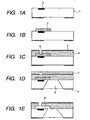
- Figs. 1A to 1E show a most advantageous process flow employing a thermally crosslinkable positive-working resist as the positive-working resist.
- Fig. 1A is a schematic cross-sectional view of a principal part showing a state in which, on a substrate 201 for example of silicon, there are formed a heat generating element 2, and a transistor for individually driving the heat generating element 2 and a circuit for a data signal processing (latter being not shown). These components are electrically connected through wirings (not shown).
- a thermally crosslinkable positive-working resist layer is coated and baked.
- the coating can be achieved by an ordinary solving coating method, such as spin coating or bar coating.
- the baking is preferably executed at a temperature of 120 to 220°C at which a thermal crosslinking reaction is executed and a period of 3 minutes to 2 hours, more preferably at 160 to 200°C and 30 minutes to 1 hour.
- an apparatus for irradiating an ultraviolet light of a short wavelength hereinafter represented as deep-UV light
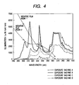
- Fig. 2 an apparatus for irradiating an ultraviolet light of a short wavelength (hereinafter represented as deep-UV light) as shown in Fig. 2 is employed to irradiate the aforementioned positive-working resist layer with a light within a region of 200 to 300 nm through a mask (not shown).
- the thermally crosslinkable positive-working resist has an absorption wavelength region in 200 to 280 nm as shown in Fig. 3 , a decomposition reaction is accelerated by a wavelength (energy distribution
- the photosensitive wavelength region of the photosensitive material (ionizing radiation sensitive resist) employed in the present invention means a wavelength region, in which, under the irradiation of an ionizing radiation of a wavelength between an upper limit and a lower limit of such region, a polymer of a main chain cleavable type absorbs such irradiation to shift to an excited state whereby a cleavage of the main chain takes place.
- a polymer of a high molecular weight is reduced to a lower molecular weight thereby showing a larger solubility in the developing liquid in a developing step to be explained later.
- the development is executed preferably with methyl isobutyl ketone which is a developing liquid for such positive-working resist, but there may be employed any solvent that dissolves an exposed portion of the positive-working resist but does not dissolve an unexposed portion thereof.
- This development process provides, as shown in Fig. 1B , a mold pattern 3 formed by the crosslinked positive-working resist.
- a negative-working photosensitive material is coated as a material for the liquid flow path structured member, so as to cover the mold pattern 3, thereby obtaining a negative-working photosensitive material layer 4.
- the coating can be achieved for example by a solvent coating method such as ordinary spin coating.
- a solvent coating method such as ordinary spin coating.
- the mold pattern 3 formed by the positive-working resist is thermally crosslinked, it is not dissolved in the coating solvent nor forms a mutual dissolution layer.
- a thin water repellent layer 5 is formed if necessary.
- Such water repellent layer 5 can be formed by a dry film method, a spin coating method or a bar coating method. It is desirable that the water repellent layer is also formed by a material having a negative-working photosensitive property.
- the material for the liquid flow path structure is, as described in Japanese Patent No. 3143307 , a material principally constituted of an epoxy resin which is solid at the normal temperature and an onium salt generating a cation under a light irradiation, and having a negative-working property.
- a photomask At the light irradiation to the liquid flow path structure material, there is employed a photomask not exposing a portion to constitute an ink discharge port 209 to the light.
- the negative-working photosensitive material layer 4 is subjected to a pattern exposure for forming an ink discharge port 209 etc.
- a pattern exposure there may be employed any ordinary exposure apparatus, but there is preferred an exposure apparatus capable of an irradiation in a wavelength region which coincides with the absorption wavelength region of the negative-working photosensitive material constituting the liquid flow path structure material and which does not overlap with absorption wavelength region of the positive-working resist material constituting the mold pattern.
- the development after the exposure is preferably executed with an aromatic solvent such as xylene.
- a water repellent is desired on the negative-working photosensitive material layer 4, such layer can be formed, as disclosed in Japanese Patent Application Laid-Open No. 2000-326515 , by forming a negative-working photosensitive water repellent layer, followed by an exposure and a development collectively. In such operation, a photosensitive water repellent layer can be formed by a lamination.
- a structure shown in Fig. 1C can be obtained by the pattern exposure on the aforementioned negative-working material for the liquid flow path structure and the material for forming the water repellent layer, followed by a development with a developing liquid. Then, as shown in Fig. 1D , after a surface at the side of the discharge port 6 is protected with a resin 7 which is provided to cover the surface bearing the discharge port 6, an anisotropic etching is executed from a rear surface of the silicon substrate with an alkali solution such as of TMAH, thereby forming an ink supply aperture 9.
- a thin film 8 for example of silicon nitride is provided as a mask for limiting an etching area in the anisotropic etching. Such film 8 can be formed prior to the formation of the heat generating element 2 etc. on the substrate 201.
- a resin such as cyclized isoprene that can protect the materials from etching and can be easily removed after the etching.
- the mold pattern 3 is irradiated, as shown in Fig. 1E , by an ionizing radiation of a wavelength of 300 nm or less across the liquid flow path structure member 4 constituted of a hardened portion by the pattern exposure to the negative-working photosensitive material layer.
- irradiation intends to decompose the crosslinked positive-working resist constituting the mold pattern 3 to a lower molecular weight, thereby enabling easy removal thereof.
- the mold pattern 3 is removed by a solvent. In this manner there is formed a liquid flow path 10 including a discharge chamber.
- the liquid flow path can be formed with an extremely precise and stable height. Also two-dimensional shapes parallel to the plane of the substrate can be realized with a submicron precision, because of the utilization of the photolithographic technology for semiconductors.
- Figs. 5 to 12 illustrate an embodiment of a configuration of a liquid discharge recording head relating to the method of the present invention and an example of the producing procedure thereof.
- the present embodiment illustrates a liquid discharge recording head having two orifices (discharge ports), but similar steps are naturally applicable to a high-density multi-array liquid discharge recording head having a larger number of orifices.
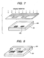
- a substrate 201 of glass, ceramics, plastics or a metal as shown in Fig. 5.
- Fig. 5 is a schematic perspective view of the substrate prior to the formation of a photosensitive material layer.
- a liquid discharge energy generating element 202 such as an electrothermal converting element or a piezoelectric element by a desired number of units ( Fig. 5 illustrating 2 units).
- Such liquid discharge energy generating element 202 provides an ink liquid with a discharge energy for causing a discharge of a small liquid droplet, thereby achieving a recording.
- These elements 202 are connected to electrodes (not shown) for entering control signals for operating these elements. Also, for the purpose of improving the durability of such discharge energy generating element 202, there are usually provided various functional layers such as a protective layer, and the presence of such functional layer is naturally acceptable also in the present invention.
- silicon is employed for the substrate 201. Since a driver and a logic circuit for controlling the discharge energy generating element are produced by an ordinary semiconductor manufacturing process, the use of silicon for the substrate is advantageous. Also for forming a through hole for ink supply in the silicon substrate, there may be applied technologies utilizing a YAG laser or sand blasting. However, in case a thermally crosslinkable resist as the material of a lower layer, such resist requires an extremely high prebake temperature far exceeding the glass transition temperature of the resin, whereby the resin film tends to hang down in the through hole. It is therefore preferred that the substrate is free from the through hole at the resist coating. In such case, there may be applied an anisotropic etching of silicon with an alkali solution. In such method, an alkali-resistant mask pattern may be formed for example with silicon nitride on the rear surface of the substrate and a membrane serving as an etching stopper may be formed with a similar material on the top surface of the substrate.
- a crosslinkable positive-working resist layer 203 is formed on the substrate 201 bearing the liquid discharge energy generating element 202.
- the resist material is a methyl methacrylate/methacrylic acid/methacrylic anhydride copolymer of a ratio of 75 : 5 : 20 (weight ratio), with a weight-averaged molecular weight (Mw) of 35,000, an average molecular weight (Mn) of 12,000 and a dispersion degree (Mw/Mn) of 2.92.
- Fig. 3 shows an absorption spectrum of the thermally crosslinkable positive-working resist material for forming the mold member. As shown in Fig.
- the positive-working resist material has an absorption spectrum only at a wavelength of 270 nm or shorter, so that an irradiation of a wavelength of 280 nm or longer does not cause a molecular excitation in the material itself in such energy region, whereby a decomposition reaction etc. is not accelerated.
- such positive-working resist material can cause a decomposition reaction only by an ionizing radiation of 270 nm or shorter and execute a pattern formation in a succeeding development process.
- a resist solution was obtained by dissolving resinous particles of the aforementioned copolymer with a solid concentration of about 30 wt.% in cyclohexanone.
- the coating solution has a viscosity of 630 cps.
- the resist solution was coated on the substrate 201 by a spin coating method, then prebaked for 3 minutes at 120°C, and further cured for 60 minutes at 200°C in an oven to execute thermal crosslinking.
- the formed film had a thickness of 14
- the thermally crosslinking positive-working resist layer 203 was subjected to a patterning (exposure and development).
- An exposure was executed with an exposure apparatus shown in Fig. 2 , and in a region of 210 to 330 nm which is a first wavelength region shown in Fig. 14 .
- the exposure amount was 60 J/cm 2
- a development was executed with methyl isobutyl ketone.
- a light of 280 nm or longer is contained in the irradiation, but does not contribute to the decomposition reaction of the positive-working resist layer as explained in the foregoing.
- a cutting filter capable of intercepting the light of 260 nm or longer as shown in Fig. 2 .
- the exposure with the ionizing radiation was executed with a photomask bearing a pattern to be left on the thermally crosslinking positive-working resist.
- an exposure apparatus having a projection optical system without an influence of a diffracted light it is naturally unnecessary to consider a line thinning in the mask design.
- a layer of a liquid flow path structure material 207 is formed so as to cover the patterned and thermally crosslinked positive-working resist layer 203.
- a coating solution for forming this layer was prepared by dissolving 50 parts of EHPE-3150 commercially supplied by Daicel Chemical Industries Ltd., 1 part of a cationic photopolymerization initiator commercially supplied by Asahi Denka Co., and 2.5 parts of a silane coupling agent A-187 commercially supplied bt Nihon Unicar Co. in 50 parts of xylene employed as a coating solvent.
- the coating was executed by spin coating, and the prebake was executed for 3 minutes at 90°C on a hot plate. Then, as shown in Fig. 9 , a pattern exposure and a development of an ink discharge port 209 are executed on the liquid flow path structure material 207.
- Such pattern exposure can be executed with any ordinary exposure apparatus capable of irradiation of a UV light.
- the irradiating light is required to have a wavelength region of 290 nm or longer, which does not overlap with the sensitive wavelength region of the mold pattern already formed by the crosslinking positive-working resist and is within the sensitive wavelength region of the negative-working film resin but which is not limited in the upper limit.
- this exposure machine emits a UV light of a region of 290 to 400 nm, in which the aforementioned negative-working film resin has a sensitivity.
- the UV light of the region of 290 to 400 nm also irradiates, as shown in Fig. 9 , the pattern of the positive-working resist layer formed in the step shown in Fig. 8 , through the negative-working film resin. Since the thermally crosslinkable positive-working resist material employed in the present invention is sensitive only to the deep-UV light of 270 nm or shorter, the decomposition reaction of the material is not accelerated in this step.
- cyclized isoprene was coated on the liquid flow path structure material layer, in order to protect such layer from an alkali solution.
- a material commercially supplied by Tokyo Oka Industries Co there was employed a material commercially supplied by Tokyo Oka Industries Co.
- the silicon substrate was immersed in a 22 wt.% solution of tetramethyl ammonium hydride (TMAH) for 14.5 hours at 83°C to form a through hole (not shown) for ink supply.
- TMAH tetramethyl ammonium hydride
- Silicon nitride employed as a mask and a membrane for forming the ink supply hole was patterned in advance on the silicon substrate.
- the silicon substrate was mounted, with the rear surface upward, on a dry etching apparatus and the membrane was removed employed a CF 4 etchant mixed with 5 % of oxygen. Then the silicon substrate was immersed in xylene to remove OBC.
- a flush irradiation of an ionizing radiation 208 of a region of 210 to 330 nm was made with a low-pressure mercury lamp toward the liquid flow path structure material 207, thereby decomposing the mold pattern constituted of the thermally crosslinking positive-working resist.
- the amount of irradiation was 81 J/cm 2 .
- the substrate 201 was immersed in methyl lactate to collectively remove the mold pattern, as shown in a vertical cross-section in Fig. 12 .
- This operation was executed in a megasonic tank of 200 MHz to shorten the dissolving time.
- a liquid flow path 211 including a discharge chamber and there is prepared an ink discharge element of a configuration in which the ink is guided from the ink supply hole 210 through each liquid flow path 211 to each discharge chamber, and is discharged from the discharge port 209 by the function of the heater.
- a crosslinkable positive-working resist layer 203 is formed on a substrate 201 bearing a liquid discharge energy generating element 202 as shown in Fig. 6 .
- the material is a methyl methacrylate/methacrylic acid/glycidyl methacrylate copolymer of a ratio of 80 : 5 : 15, with a weight-averaged molecular weight (Mw) of 34,000, an average molecular weight (Mn) of 11,000 and a dispersion degree (Mw/Mn) of 3.09.
- Fig. 15 shows an absorption spectrum of the thermally crosslinkable positive-working resist material for forming the mold member. As shown in Fig.
- the positive-working resist material has an absorption spectrum only at a wavelength of 260 nm or shorter, so that an irradiation of a wavelength of 270 nm or longer does not cause a molecular excitation in the material itself in such energy region, whereby a decomposition reaction etc. is not accelerated.
- such positive-working resist material can cause a decomposition reaction only by an ionizing radiation of 260 nm or shorter and execute a pattern formation in a succeeding development process.
- a resist solution was obtained by dissolving resinous particles of the aforementioned copolymer with a solid concentration of about 30 wt.% in cyclohexanone.
- the coating solution has a viscosity of 630 cps.
- the resist solution was coated on the substrate 201 by a spin coating method, then prebaked for 3 minutes at 120°C, and further cured for 60 minutes at 200°C in an oven to execute thermal crosslinking.
- the formed film had a thickness of 14
- a liquid flow path 211 including a discharge chamber in a similar manner as in the first embodiment, whereby obtained is an ink discharge element of a configuration in which the ink is guided from the ink supply hole 210 through each liquid flow path 211 to each discharge chamber, and is discharged from the discharge port 209 by the function of the heater.
- a crosslinkable positive-working resist layer 203 is formed on a substrate 201 bearing a liquid discharge energy generating element 202 as shown in Fig. 6 .
- the material is a methyl methacrylate/methacrylic acid/methyl 3-oxyimino-2-butanone methacrylate copolymer of a ratio of 85 : 5 : 10, with a weight-averaged molecular weight (Mw) of 35,000, an average molecular weight (Mn) of 13,000 and a dispersion degree (Mw/Mn) of 2.69.
- Fig. 16 shows an absorption spectrum of the thermally crosslinkable positive-working resist material for forming the mold member. As shown in Fig.
- the positive-working resist material has an absorption spectrum only at a wavelength of 260 nm or shorter, so that an irradiation of a wavelength of 270 nm or longer does not cause a molecular excitation in the material itself in such energy region, whereby a decomposition reaction etc. is not accelerated.
- such positive-working resist material can cause a decomposition reaction only by an ionizing radiation of 260 nm or shorter and execute a pattern formation in a succeeding development process.
- a resist solution was obtained by dissolving resinous particles of the aforementioned copolymer with a solid concentration of about 30 wt.% in cyclohexanone.
- the coating solution has a viscosity of 630 cps.
- the resist solution was coated on the substrate 201 by a spin coating method, then prebaked for 3 minutes at 120°C, and further cured for 60 minutes at 200°C in an oven to execute thermal crosslinking.
- the formed film had a thickness of 14
- a liquid flow path 211 including a discharge chamber in a similar manner as in the first embodiment, whereby obtained is an ink discharge element of a configuration in which the ink is guided from the ink supply hole 210 through each liquid flow path 211 to each discharge chamber, and is discharged from the discharge port 209 by the function of the heater.
- a crosslinkable positive-working resist layer 203 is formed on a substrate 201 bearing a liquid discharge energy generating element 202.
- the material is a methyl methacrylate/methacrylic acid/methacryonitrile copolymer of a ratio of 75 : 5 : 20, with a weight-averaged molecular weight (Mw) of 30,000, an average molecular weight (Mn) of 16,000 and a dispersion degree (Mw/Mn) of 1.88.
- Fig. 17 shows an absorption spectrum of the thermally crosslinkable positive-working resist material for forming the mold member. As shown in Fig.
- the positive-working resist material has an absorption spectrum only at a wavelength of 260 nm or shorter, so that an irradiation of a wavelength of 270 nm or longer does not cause a molecular excitation in the material itself in such energy region, whereby a decomposition reaction etc. is not accelerated.
- such positive-working resist material can cause a decomposition reaction only by an ionizing radiation of 260 nm or shorter and execute a pattern formation in a succeeding development process.
- a resist solution was obtained by dissolving resinous particles of the aforementioned copolymer with a solid concentration of about 30 wt.% in cyclohexanone.
- the coating solution has a viscosity of 630 cps.
- the resist solution was coated on the substrate 201 by a spin coating method, then prebaked for 3 minutes at 120°C, and further cured for 60 minutes at 200°C in an oven to execute thermal crosslinking.
- the formed film had a thickness of 14
- a liquid flow path 211 including a discharge chamber in a similar manner as in the first embodiment, whereby obtained is an ink discharge element of a configuration in which the ink is guided from the ink supply hole 210 through each liquid flow path 211 to each discharge chamber, and is discharged from the discharge port 209 by the function of the heater.
- a crosslinkable positive-working resist layer 203 is formed on a substrate 201 bearing a liquid discharge energy generating element 202.
- the material is a methyl methacrylate/methacrylic acid/fumaric anhydride copolymer of a ratio of 80 : 5 : 15, with a weight-averaged molecular weight (Mw) of 30,000, an average molecular weight (Mn) of 14,000 and a dispersion degree (Mw/Mn) of 2.14.
- Fig. 18 shows an absorption spectrum of the thermally crosslinkable positive-working resist material for forming the mold member. As shown in Fig.
- the positive-working resist material has an absorption spectrum only at a wavelength of 260 nm or shorter, so that an irradiation of a wavelength of 270 nm or longer does not cause a molecular excitation in the material itself in such energy region, whereby a decomposition reaction etc. is not accelerated.
- such positive-working resist material can cause a decomposition reaction only by an ionizing radiation of 260 nm or shorter and execute a pattern formation in a succeeding development process.
- a resist solution was obtained by dissolving resinous particles of the aforementioned copolymer with a solid concentration of about 30 wt.% in cyclohexanone.
- the coating solution has a viscosity of 630 cps.
- the resist solution was coated on the substrate 201 by a spin coating method, then prebaked for 3 minutes at 120°C, and further cured for 60 minutes at 200°C in an oven to execute thermal crosslinking.
- the formed film had a thickness of 14
- a liquid flow path 211 including a discharge chamber in a similar manner as in the first embodiment, whereby obtained is an ink discharge element of a configuration in which the ink is guided from the ink supply hole 210 through each liquid flow path 211 to each discharge chamber, and is discharged from the discharge port 209 by the function of the heater.
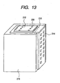
- the discharge element thus prepared was assembled in an ink jet head unit of a configuration shown in Fig. 13 , and was subjected an evaluation of discharge and recording, in which a satisfactory image recording was possible.
- a TAB film 214 for exchanging recording signals with a main body of the recording apparatus is provided on an external surface of a supporting member which detachably supports an ink tank 213, and an ink discharge element 212 is connected with electric wirings on the TAB film 214 by electric connecting leads 215.
- a substrate 201 is prepared. Most commonly, silicon is employed for the substrate 201. Since a driver and a logic circuit for controlling the discharge energy generating element are produced by an ordinary semiconductor manufacturing process, the use of silicon for the substrate is advantageous.
- silicon substrate bearing an electrothermal converting element (a heater composed of HfB 2 ) as the ink discharge pressure generating element 202, and a deposition film of SiN + Ta (not shown) in portions for forming an ink flow path and a nozzle.
- a positive-working resist layer is formed, and is patterned to form a flow path pattern 203.
- the positive-working resist there was employed a following photodegradable positive-working resist:
- This resin in powder state was dissolved with a solid concentration of about 30 wt.% in cyclohexanone and was used as a resist solution.
- the resist solution had a viscosity of 630 cps.
- This resist solution was coated by a spin coating method, then prebaked for 3 minutes at 120°C, and was heat treated for 60 minutes at 250°C in a nitrogen atmosphere in an oven.
- the resist layer after the heat treatment had a thickness of 12 ⁇ m.
- the exposure and the development were conducted under following conditions.
- a photosensitive resin composition of a following composition was spin coated on the processed substrate (film thickness of 20 ⁇ m on the substrate), and was baked for 2 minutes at 100°C (hot plate) to form a liquid flow path structure material 207: EHPE (Daicel Chemical Industries Ltd.) 100 parts by weight 1,4HFAB (Central Glass Co.) 20 parts by weight SP-170 (Asahi Denka Industries Co.) 2 parts by weight A-187 (Nihon Unicar Inc.) 5 parts by weight Methyl isobutyl ketone 100 parts by weight Diglyme 100 parts by weight
- a photosensitive resin composition of a following composition was spin coated on the processed substrate so as to obtain a film thickness of 1 ⁇ m, and was baked for 3 minutes at 80°C (hot plate) to form an ink repellent layer:
- EHPE Denicel Chemical Industries Ltd. 35 parts by weight 2,2-bis(4-glycidyloxyphenyl)hexafluoropropane 25 parts by weight 1,4-bis(2-hydroxyhexafluoroisopropyl)benzene 25 parts by weight 3-(2-perfluorohexyl)ethoxy-1,2-epoxypropane 16 parts by weight A-187 (Nihon Unicar Inc.) 4 parts by weight SP-170 (Asahi Denka Industries Co.) 2 parts by weight Diethylene glycol monoethyl ether 100 parts by weight
- liquid flow path structure material 207 and the ink repellent layer were patterned by a pattern exposure by MPA-600 (manufactured by Canon Inc.) with a light of a wavelength of 290 to 400 nm and with an exposure amount of 400 mJ/cm 2 , then a post-exposure bake for 120 seconds at 120°C on a hot plate and a development with methyl isobutyl ketone to form an ink discharge port 209.
- MPA-600 manufactured by Canon Inc.
- an etching mask 7 having an aperture of a width of 1 mm and a length of 10 mm was prepared with a polyetheramide composition (HIMAL, manufactured by Hitachi Chemical Co.). Then the substrate was subjected to an anisotropic etching by immersion in a 22 wt.% TMAH aqueous solution maintained at 80°C, thereby forming an ink supply aperture 210. In this operation, in order to protect the ink repellent layer 5 from the etching solution, the anisotropic etching was conducted after coating a protective film (OBC manufactured by Tokyo Oka Industries Co.; not shown) on the ink repellent layer.
- OBC protective film
- the ink jet head thus prepared was mounted on a printer and subjected to an evaluation of discharge and recording, in which a satisfactory image recording was possible.
- An ink jet head was prepared in the same manner as in the embodiment 6 except that a following photodegradable positive-working resist was employed, and was subjected to an evaluation of discharge and recording, in which a satisfactory image recording was possible:
- An ink jet head was prepared in the same manner as in the embodiment 6 except that a following photodegradable positive-working resist was employed, and was subjected to an evaluation of discharge and recording, in which a satisfactory image recording was possible:
Applications Claiming Priority (4)
| Application Number | Priority Date | Filing Date | Title |
|---|---|---|---|
| JP2002201894 | 2002-07-10 | ||
| JP2002201894 | 2002-07-10 | ||
| JP2003271624A JP4298414B2 (ja) | 2002-07-10 | 2003-07-07 | 液体吐出ヘッドの製造方法 |
| JP2003271624 | 2003-07-07 |
Publications (2)
| Publication Number | Publication Date |
|---|---|
| EP1380423A1 EP1380423A1 (en) | 2004-01-14 |
| EP1380423B1 true EP1380423B1 (en) | 2009-04-15 |
Family
ID=29738475
Family Applications (1)
| Application Number | Title | Priority Date | Filing Date |
|---|---|---|---|
| EP03015757A Expired - Lifetime EP1380423B1 (en) | 2002-07-10 | 2003-07-10 | Method for producing fine structured member, method for producing fine hollow structured member and method for producing liquid discharge head |
Country Status (7)
| Country | Link |
|---|---|
| US (1) | US7592131B2 (ja) |
| EP (1) | EP1380423B1 (ja) |
| JP (1) | JP4298414B2 (ja) |
| KR (1) | KR100541904B1 (ja) |
| CN (1) | CN1229228C (ja) |
| DE (1) | DE60327133D1 (ja) |
| TW (1) | TWI225448B (ja) |
Families Citing this family (18)
| Publication number | Priority date | Publication date | Assignee | Title |
|---|---|---|---|---|
| JP4447974B2 (ja) * | 2004-06-28 | 2010-04-07 | キヤノン株式会社 | インクジェットヘッドの製造方法 |
| EP1763706B1 (en) | 2004-06-28 | 2013-12-11 | Canon Kabushiki Kaisha | Method for manufacturing liquid discharge head |
| CN1968815B (zh) * | 2004-06-28 | 2013-05-01 | 佳能株式会社 | 排液头制造方法,和使用该方法得到的排液头 |
| JP4761498B2 (ja) | 2004-06-28 | 2011-08-31 | キヤノン株式会社 | 感光性樹脂組成物、ならびにこれを用いた段差パターンの製造方法及びインクジェットヘッドの製造方法 |
| JP4484774B2 (ja) * | 2004-06-28 | 2010-06-16 | キヤノン株式会社 | 液体吐出ヘッドの製造方法 |
| JP4480141B2 (ja) * | 2004-06-28 | 2010-06-16 | キヤノン株式会社 | インクジェット記録ヘッドの製造方法 |
| JP4533256B2 (ja) * | 2004-06-28 | 2010-09-01 | キヤノン株式会社 | 微細構造体の製造方法および液体吐出ヘッドの製造方法 |
| DE602005015974D1 (de) * | 2004-06-28 | 2009-09-24 | Canon Kk | Kopfs und unter verwendung dieses verfahrens erhaltener flüssigkeitsabgabekopf |
| JP2006126116A (ja) * | 2004-11-01 | 2006-05-18 | Canon Inc | フィルター用基板の製造方法、インクジェット記録ヘッドおよびその製造方法 |
| US7824560B2 (en) * | 2006-03-07 | 2010-11-02 | Canon Kabushiki Kaisha | Manufacturing method for ink jet recording head chip, and manufacturing method for ink jet recording head |
| US8376525B2 (en) * | 2006-09-08 | 2013-02-19 | Canon Kabushiki Kaisha | Liquid discharge head and method of manufacturing the same |
| US7550252B2 (en) * | 2006-09-21 | 2009-06-23 | Canon Kabushiki Kaisha | Ink-jet recording head and method for producing same |
| US8499453B2 (en) * | 2009-11-26 | 2013-08-06 | Canon Kabushiki Kaisha | Method of manufacturing liquid discharge head, and method of manufacturing discharge port member |
| JP5473645B2 (ja) | 2010-02-05 | 2014-04-16 | キヤノン株式会社 | 感光性樹脂組成物及び液体吐出ヘッド |
| US8434229B2 (en) * | 2010-11-24 | 2013-05-07 | Canon Kabushiki Kaisha | Liquid ejection head manufacturing method |
| KR101249723B1 (ko) * | 2011-10-28 | 2013-04-02 | 전자부품연구원 | 액적 토출용 노즐 제조 방법 및 이를 이용해 제조된 노즐을 이용한 정전식 액적 토출 장치 |
| CN103935127B (zh) * | 2014-04-24 | 2017-01-11 | 珠海赛纳打印科技股份有限公司 | 液体喷头制造方法、液体喷头和打印装置 |
| JP6217711B2 (ja) * | 2015-08-21 | 2017-10-25 | 日亜化学工業株式会社 | 発光装置の製造方法 |
Family Cites Families (18)
| Publication number | Priority date | Publication date | Assignee | Title |
|---|---|---|---|---|
| US4087569A (en) * | 1976-12-20 | 1978-05-02 | International Business Machines Corporation | Prebaking treatment for resist mask composition and mask making process using same |
| US4330614A (en) * | 1980-10-14 | 1982-05-18 | International Business Machines Corporation | Process for forming a patterned resist mask |
| JPH0645242B2 (ja) * | 1984-12-28 | 1994-06-15 | キヤノン株式会社 | 液体噴射記録ヘツドの製造方法 |
| DE3764702D1 (de) | 1986-04-24 | 1990-10-11 | Ibm | Zwei-schichten-photolack-verfahren mit deckschicht. |
| US5264874A (en) * | 1990-02-09 | 1993-11-23 | Canon Kabushiki Kaisha | Ink jet recording system |
| DE69127801T2 (de) | 1990-12-19 | 1998-02-05 | Canon Kk | Herstellungsverfahren für flüssigkeitsausströmenden Aufzeichnungskopf |
| JP2925816B2 (ja) | 1991-10-31 | 1999-07-28 | キヤノン株式会社 | 液体噴射記録ヘッド、その製造方法、及び同ヘッドを具備した記録装置 |
| CA2075097C (en) * | 1991-08-02 | 2000-03-28 | Hiroyuki Ishinaga | Recording apparatus, recording head and substrate therefor |
| DE69329359T2 (de) | 1992-06-01 | 2001-03-08 | Canon Kk | Verfahren zur Herstellung eines Tintenstrahlaufzeichnungskopfes |
| JP2960608B2 (ja) | 1992-06-04 | 1999-10-12 | キヤノン株式会社 | 液体噴射記録ヘッドの製造方法 |
| JP3305415B2 (ja) * | 1992-06-18 | 2002-07-22 | キヤノン株式会社 | 半導体装置、インクジェットヘッド、および画像形成装置 |
| JPH0645242A (ja) | 1992-07-24 | 1994-02-18 | Hitachi Ltd | レジスト塗布方法及びその装置 |
| JP3143307B2 (ja) | 1993-02-03 | 2001-03-07 | キヤノン株式会社 | インクジェット記録ヘッドの製造方法 |
| US6461798B1 (en) | 1995-03-31 | 2002-10-08 | Canon Kabushiki Kaisha | Process for the production of an ink jet head |
| JP3347530B2 (ja) | 1995-06-27 | 2002-11-20 | 富士通株式会社 | レジスト組成物及びレジストパターンの形成方法 |
| DE19701189B4 (de) * | 1996-01-18 | 2005-06-30 | International Rectifier Corp., El Segundo | Halbleiterbauteil |
| EP0816082B1 (en) * | 1996-06-26 | 2005-05-18 | Canon Kabushiki Kaisha | Recording head and recording apparatus using the same |
| JP4497633B2 (ja) | 1999-03-15 | 2010-07-07 | キヤノン株式会社 | 撥液体層の形成方法及び液体吐出ヘッドの製造方法 |
-
2003
- 2003-07-07 JP JP2003271624A patent/JP4298414B2/ja not_active Expired - Fee Related
- 2003-07-09 US US10/615,289 patent/US7592131B2/en not_active Expired - Fee Related
- 2003-07-10 KR KR1020030046777A patent/KR100541904B1/ko not_active IP Right Cessation
- 2003-07-10 TW TW092118893A patent/TWI225448B/zh not_active IP Right Cessation
- 2003-07-10 CN CNB031467873A patent/CN1229228C/zh not_active Expired - Fee Related
- 2003-07-10 DE DE60327133T patent/DE60327133D1/de not_active Expired - Lifetime
- 2003-07-10 EP EP03015757A patent/EP1380423B1/en not_active Expired - Lifetime
Also Published As
| Publication number | Publication date |
|---|---|
| KR100541904B1 (ko) | 2006-01-10 |
| JP2004042650A (ja) | 2004-02-12 |
| KR20040005699A (ko) | 2004-01-16 |
| TWI225448B (en) | 2004-12-21 |
| JP4298414B2 (ja) | 2009-07-22 |
| TW200410831A (en) | 2004-07-01 |
| DE60327133D1 (de) | 2009-05-28 |
| US7592131B2 (en) | 2009-09-22 |
| CN1475352A (zh) | 2004-02-18 |
| US20040072107A1 (en) | 2004-04-15 |
| CN1229228C (zh) | 2005-11-30 |
| EP1380423A1 (en) | 2004-01-14 |
Similar Documents
| Publication | Publication Date | Title |
|---|---|---|
| EP1768847B1 (en) | Liquid discharge head manufacturing method, and liquid discharge head obtained using this method | |
| EP1768848B1 (en) | Liquid discharge head manufacturing method, and liquid discharge head obtained using this method | |
| EP1380425B1 (en) | Method of producing microstructure, and method of producing liquid discharge head | |
| EP1380423B1 (en) | Method for producing fine structured member, method for producing fine hollow structured member and method for producing liquid discharge head | |
| US6951380B2 (en) | Method of manufacturing microstructure, method of manufacturing liquid discharge head, and liquid discharge head | |
| EP1766475B1 (en) | Method of forming level difference pattern using the photosensitive resin composition, and method of producing ink jet head | |
| EP1763440B1 (en) | Ink jet head manufacturing method and ink jet head manufactured by the manufacturing method | |
| EP1763705B1 (en) | Ink jet head using photosensitive resin composition, and process for manufacturing ink jet head | |
| JP5159823B2 (ja) | 構造体の製造方法および液体吐出ヘッドの製造方法 | |
| JP2009119650A (ja) | インクジェットヘッドの製造方法 | |
| JP2009096036A (ja) | 記録ヘッド基板及びその製造方法 | |
| JP4533256B2 (ja) | 微細構造体の製造方法および液体吐出ヘッドの製造方法 | |
| US20050046662A1 (en) | Ink jet recording head and method for manufacturing the same | |
| JP2004042396A (ja) | 微細構造体の製造方法、液体吐出ヘッドの製造方法および液体吐出ヘッド | |
| JP2006069009A (ja) | インクジェットヘッドの製造方法 | |
| KR20070022805A (ko) | 액체 토출 헤드 제조 방법, 및 이러한 방법을 사용하여얻어지는 액체 토출 헤드 |
Legal Events
| Date | Code | Title | Description |
|---|---|---|---|
| PUAI | Public reference made under article 153(3) epc to a published international application that has entered the european phase |
Free format text: ORIGINAL CODE: 0009012 |
|
| AK | Designated contracting states |
Kind code of ref document: A1 Designated state(s): AT BE BG CH CY CZ DE DK EE ES FI FR GB GR HU IE IT LI LU MC NL PT RO SE SI SK TR |
|
| AX | Request for extension of the european patent |
Extension state: AL LT LV MK |
|
| 17P | Request for examination filed |
Effective date: 20040714 |
|
| AKX | Designation fees paid |
Designated state(s): DE FR GB IT |
|
| 17Q | First examination report despatched |
Effective date: 20040910 |
|
| 17Q | First examination report despatched |
Effective date: 20040910 |
|
| 17Q | First examination report despatched |
Effective date: 20040910 |
|
| GRAP | Despatch of communication of intention to grant a patent |
Free format text: ORIGINAL CODE: EPIDOSNIGR1 |
|
| GRAS | Grant fee paid |
Free format text: ORIGINAL CODE: EPIDOSNIGR3 |
|
| GRAA | (expected) grant |
Free format text: ORIGINAL CODE: 0009210 |
|
| AK | Designated contracting states |
Kind code of ref document: B1 Designated state(s): DE FR GB IT |
|
| REG | Reference to a national code |
Ref country code: GB Ref legal event code: FG4D |
|
| REF | Corresponds to: |
Ref document number: 60327133 Country of ref document: DE Date of ref document: 20090528 Kind code of ref document: P |
|
| PLBE | No opposition filed within time limit |
Free format text: ORIGINAL CODE: 0009261 |
|
| STAA | Information on the status of an ep patent application or granted ep patent |
Free format text: STATUS: NO OPPOSITION FILED WITHIN TIME LIMIT |
|
| 26N | No opposition filed |
Effective date: 20100118 |
|
| REG | Reference to a national code |
Ref country code: FR Ref legal event code: ST Effective date: 20100331 |
|
| PG25 | Lapsed in a contracting state [announced via postgrant information from national office to epo] |
Ref country code: FR Free format text: LAPSE BECAUSE OF NON-PAYMENT OF DUE FEES Effective date: 20090731 |
|
| PG25 | Lapsed in a contracting state [announced via postgrant information from national office to epo] |
Ref country code: IT Free format text: LAPSE BECAUSE OF FAILURE TO SUBMIT A TRANSLATION OF THE DESCRIPTION OR TO PAY THE FEE WITHIN THE PRESCRIBED TIME-LIMIT Effective date: 20090415 |
|
| PGFP | Annual fee paid to national office [announced via postgrant information from national office to epo] |
Ref country code: GB Payment date: 20150727 Year of fee payment: 13 Ref country code: DE Payment date: 20150731 Year of fee payment: 13 |
|
| REG | Reference to a national code |
Ref country code: DE Ref legal event code: R119 Ref document number: 60327133 Country of ref document: DE |
|
| GBPC | Gb: european patent ceased through non-payment of renewal fee |
Effective date: 20160710 |
|
| PG25 | Lapsed in a contracting state [announced via postgrant information from national office to epo] |
Ref country code: DE Free format text: LAPSE BECAUSE OF NON-PAYMENT OF DUE FEES Effective date: 20170201 |
|
| PG25 | Lapsed in a contracting state [announced via postgrant information from national office to epo] |
Ref country code: GB Free format text: LAPSE BECAUSE OF NON-PAYMENT OF DUE FEES Effective date: 20160710 |