EP1320897B1 - Verfahren zum herstellen eines halbleiterbauelements aus halbleitermaterial mit reduzierter mittlerer freier weglänge und mit dem verfahren hergestelltes halbleiterbauelement - Google Patents
Verfahren zum herstellen eines halbleiterbauelements aus halbleitermaterial mit reduzierter mittlerer freier weglänge und mit dem verfahren hergestelltes halbleiterbauelement Download PDFInfo
- Publication number
- EP1320897B1 EP1320897B1 EP01985777A EP01985777A EP1320897B1 EP 1320897 B1 EP1320897 B1 EP 1320897B1 EP 01985777 A EP01985777 A EP 01985777A EP 01985777 A EP01985777 A EP 01985777A EP 1320897 B1 EP1320897 B1 EP 1320897B1
- Authority
- EP
- European Patent Office
- Prior art keywords
- crystal layer
- crystal
- free path
- mean free
- path length
- Prior art date
- Legal status (The legal status is an assumption and is not a legal conclusion. Google has not performed a legal analysis and makes no representation as to the accuracy of the status listed.)
- Expired - Lifetime
Links
- 239000004065 semiconductor Substances 0.000 title claims description 94
- 239000000463 material Substances 0.000 title claims description 72
- 238000004519 manufacturing process Methods 0.000 title claims description 6
- 239000013078 crystal Substances 0.000 claims description 185
- 239000000758 substrate Substances 0.000 claims description 39
- 239000002800 charge carrier Substances 0.000 claims description 37
- 239000013256 coordination polymer Substances 0.000 claims description 28
- 238000000034 method Methods 0.000 claims description 12
- 230000005684 electric field Effects 0.000 claims description 6
- 229910052710 silicon Inorganic materials 0.000 claims description 6
- 239000010703 silicon Substances 0.000 claims description 6
- 125000004432 carbon atom Chemical group C* 0.000 claims description 5
- GNPVGFCGXDBREM-UHFFFAOYSA-N germanium atom Chemical group [Ge] GNPVGFCGXDBREM-UHFFFAOYSA-N 0.000 claims description 5
- 230000000903 blocking effect Effects 0.000 claims description 4
- 239000012535 impurity Substances 0.000 description 16
- 239000002245 particle Substances 0.000 description 16
- 239000000969 carrier Substances 0.000 description 8
- 238000000407 epitaxy Methods 0.000 description 6
- 230000006798 recombination Effects 0.000 description 6
- 238000005215 recombination Methods 0.000 description 6
- 125000004429 atom Chemical group 0.000 description 2
- 230000007547 defect Effects 0.000 description 2
- 239000002019 doping agent Substances 0.000 description 2
- 239000012071 phase Substances 0.000 description 2
- 240000001439 Opuntia Species 0.000 description 1
- 235000004727 Opuntia ficus indica Nutrition 0.000 description 1
- QVGXLLKOCUKJST-UHFFFAOYSA-N atomic oxygen Chemical compound [O] QVGXLLKOCUKJST-UHFFFAOYSA-N 0.000 description 1
- 150000001875 compounds Chemical class 0.000 description 1
- 238000009792 diffusion process Methods 0.000 description 1
- 238000005530 etching Methods 0.000 description 1
- 229910052732 germanium Inorganic materials 0.000 description 1
- 238000005304 joining Methods 0.000 description 1
- 239000007791 liquid phase Substances 0.000 description 1
- 238000001451 molecular beam epitaxy Methods 0.000 description 1
- 230000007935 neutral effect Effects 0.000 description 1
- 229910052760 oxygen Inorganic materials 0.000 description 1
- 239000001301 oxygen Substances 0.000 description 1
- 238000005498 polishing Methods 0.000 description 1
- 229910021420 polycrystalline silicon Inorganic materials 0.000 description 1
- 239000002244 precipitate Substances 0.000 description 1
- 238000002360 preparation method Methods 0.000 description 1
- 239000000126 substance Substances 0.000 description 1
- 230000007704 transition Effects 0.000 description 1
Images


Classifications
-
- H—ELECTRICITY
- H10—SEMICONDUCTOR DEVICES; ELECTRIC SOLID-STATE DEVICES NOT OTHERWISE PROVIDED FOR
- H10D—INORGANIC ELECTRIC SEMICONDUCTOR DEVICES
- H10D8/00—Diodes
-
- H—ELECTRICITY
- H10—SEMICONDUCTOR DEVICES; ELECTRIC SOLID-STATE DEVICES NOT OTHERWISE PROVIDED FOR
- H10D—INORGANIC ELECTRIC SEMICONDUCTOR DEVICES
- H10D62/00—Semiconductor bodies, or regions thereof, of devices having potential barriers
- H10D62/50—Physical imperfections
- H10D62/53—Physical imperfections the imperfections being within the semiconductor body
-
- H—ELECTRICITY
- H10—SEMICONDUCTOR DEVICES; ELECTRIC SOLID-STATE DEVICES NOT OTHERWISE PROVIDED FOR
- H10D—INORGANIC ELECTRIC SEMICONDUCTOR DEVICES
- H10D62/00—Semiconductor bodies, or regions thereof, of devices having potential barriers
- H10D62/60—Impurity distributions or concentrations
Definitions
- the invention relates to a method of manufacturing a semiconductor device having a body of doped semiconductor material with a given mean free path for free carriers and a mean free path for the free carriers that is smaller than the determined mean free path.
- This body has a junction between doped semiconductor material of a conductivity type and doped semiconductor material of a conductivity type opposite to the conductivity type.
- the smaller mean free path increases the body's ability to lock.
- the US 5,858,855 describes a device in which additional layers of polycrystalline silicon are present to reduce the minority charge lifetime.
- the EP 0 889 509 describes a semiconductor device in which only interface lattice defects are used as recombination centers.
- the WO 00/07245 discloses a power semiconductor device having a recombination region having recombination centers comprising oxygen precipitates.
- the WO 98/15010 discloses a thyristor having a recombination zone for reduced free carrier lifetime.
- the object of the invention is to provide a simple method for producing a semiconductor device with a body of the type mentioned, which has only a locally and not over the entire body extending region reduced average free path, and provide a corresponding Halbeiterbauelement available.
- the scattering centers reduce the determined mean free path for the free charge carriers of the crystal layer, so that the crystal layer with the scattering centers has a smaller mean free path for the free charge carriers.
- the scattering centers can be distributed over the entire surface of the crystal layer, so that the mean free path of the crystal layer over the entire surface of the crystal layer advantageously, they may be present only locally at one or more particular locations of the surface of the crystal layer so that the mean free path is reduced only over a portion of the area of the crystal layer.
- the reduced mean free path is essentially limited only to the extent of the crystal layer and does not extend to areas of the body outside the crystal layer.
- Non-doping means that the impurity particles have no influence on a conductivity of the doped semiconductor material into which they are introduced.
- the foreign substance particles act in the semiconductor material merely as scattering centers which reduce the mean free path already present in the semiconductor material.
- Scattering centers are generated by adding non-doping germanium and / or carbon atoms during growth of the crystal layer in the crystal layer.
- an amount of non-doping impurity particles offered for the production of scattering centers in the crystal layer is temporally varied. As a result, it is advantageously possible to obtain a local variation of the reduced mean free path in the direction vertical to the surface of the crystal layer.
- scattering centers can also be produced by diffusing non-doping impurity particles into the crystal layer.
- further doped semiconductor material is applied to the crystal layer having the smaller mean free path for the free carriers, which has an average free path for the free carriers that is equal to or greater than the determined mean free path for the free carriers.
- the further doped semiconductor material may advantageously comprise at least one crystal layer of doped semiconductor material grown by epitaxy on the crystal layer with the smaller mean free path, it may also comprise a crystal body of doped semiconductor material which is connected by wafer bonding with an exposed crystal layer on the substrate crystal.
- the crystal body may accordingly be connected to the crystal layer having the smaller mean free path or to a crystal layer grown on this crystal layer.
- the further doped semiconductor material has a conductivity type opposite to a conductivity type of the substrate crystal.
- a crystal layer of doped semiconductor material is grown on a surface of a substrate crystal 10 of doped semiconductor material, for example on the upwardly facing surface 11 of the crystal 10, by epitaxy, wherein the semiconductor material is silicon.
- the doped semiconductor material of the substrate crystal 10 is, for example, n-doped and has a certain mean free path for free charge carriers CP, for the most part electrons in the example. If the semiconductor material of the substrate crystal 10 is p-doped, the free charge carriers CP are largely holes.
- the determined mean free path for the free charge carriers CP of the substrate crystal 10 is, for example, the mean free path length ⁇ n for the free charge carriers CP that is naturally present in the doped semiconductor material of the substrate crystal 10.
- the doped semiconductor material of the crystal layer to be grown is selected, for example, of the same conductivity type as the doped semiconductor material of the substrate crystal 10, in the example thus n-doped.
- the doped semiconductor material of the crystal layer to be grown on a certain average free path for the free charge carriers CP which is naturally present in the doped semiconductor material of the growing crystal layer mean free path for the free charge carriers CP, in the example for the most part Electrons, can be.
- the semiconductor material of the crystal layer to be grown is selected to be so different from the semiconductor material of the substrate crystal 10 that the determined mean free path for the free charge carriers CP of the crystal layer to be grown is smaller than the determined mean free path length for the same free charge carriers CP of the substrate crystal 10, then can realize a device according to the invention be.
- the same doped semiconductor material as used for the substrate crystal 10 which has the same specific mean free path ⁇ n for the same free charge carriers CP for at least this part of the crystal layer to be grown and the substrate crystal 10, and the comparatively smaller mean free path for the same free carrier CP is produced by creating scattering centers in the crystal layer which reduce the determined mean free path for the free charge carriers CP of the crystal layer.
- the scattering centers in the crystal layer are formed by introducing non-dopant impurity particles into the crystal layer, namely, by adding non-dopant impurity particles during growth of the crystal layer to this layer.
- FIG. 2 shows the substrate crystal 10 during the epitaxial growth of the crystal layer on the surface 11 of the substrate crystal 10, wherein an adjacent to the substrate crystal 10 part of the designated 20 crystal layer on this surface 11 has already grown.
- liquid-phase, gas-phase and / or molecular-beam epitaxy can be used to grow the crystal layer 20.
- phase and / or the molecular beam for example, the non-doping impurity particles, for example, non-doping impurity atoms added, which in the FIG. 2 are indicated by dots 21 and define scattering centers 21 'in the crystal layer 20 grown on the surface 11 of the substrate crystal.
- FIG. 3 illustrated exemplary body 1 with the crystal layer 20, in which the introduced mean scattering centers 21 'the specific mean free path ⁇ n for the free charge carriers CP is reduced to the smaller mean free path ⁇ r for these charge carriers CP.
- the non-doping scattering centers 21 ' may be distributed over the entire surface of the crystal layer 20 in the layer 20, for example uniformly.
- This surface is represented, for example, by the surface 201 of the crystal layer 20 facing away from the substrate crystal 10. In this case, the mean free path for the free carriers is reduced over the entire surface 201.
- the scattering centers 21 ' can also be distributed over only one or more subregions of the surface 201 in the crystal layer 20 and be absent outside of these subregions.
- the mean free path for the free charge carriers is reduced only over the subarea or subregions and, outside of these subareas, the determined mean free path length ⁇ n for the free charge carriers CP is present in the layer 20.
- an amount of non-doping impurity particles 21 offered for producing scattering centers 21 'in the crystal layer 20 is varied over time.
- the substrate crystal 10 and the crystal layer 20 are each made of silicon, and the scattering centers 21 'are defined by impurity particles 21 in the form of germanium atoms and / or carbon atoms.
- scattering centers 21 ' may be generated by in-diffusion of nondoped impurity particles 21 after completion of the epitaxy into the finished crystal layer 20.
- a part 20 'bordering the surface 11 of the substrate crystal 10 consists of semiconductor material of the same conductivity type as the semiconductor material of the crystal body 10 of the crystal layer 20, in the example of the conductivity type n, and to a surface 202 of this part 20 facing away from the surface 11 of the substrate crystal 10
- the crystal layer 20 and thus the body 1 has a pn junction 100 between p-doped semiconductor material and n-doped semiconductor material.
- This junction 100 extends in the interface between the n-doped semiconductor material and the p-doped semiconductor material of the crystal layer 20, d. H. in the surface 202 of the crystal layer 20.
- FIG. 4 3 a development of the body 1 according to FIG. 3 is shown in such a way that further doped semiconductor material 30 of the body 1 is applied to the crystal layer 20 of the body 1, which has the smaller mean free path ⁇ r for the free charge carriers CP, which has a mean free path length for the free charge carriers CP, which is greater than the smaller mean free path ⁇ r for the free charge carriers CP of the crystal layer 20.
- the further doped semiconductor material 30 of the body 1 may, for example, at least one of epitaxy on the Surface 201 of the crystal layer 20 with the smaller mean free path ⁇ r grown crystal layer of doped semiconductor material exist.
- the semiconductor material 30 can also consist of a single crystal crystalline body of doped semiconductor material similar to, for example, the substrate crystal 10, which is connected by wafer bonding to an exposed crystal layer on the substrate crystal 10.
- the surface 31 of the crystal body 30 facing the crystal layer 20 and the surface 201 of the crystal layer 20 are bonded together, the joint 23 between the two surfaces 31 and 201 being made by wafer bonding.
- Wafer bonding per se is a known joining technique (see eg Q.-Y. Tong, "Wafer Bonds and Wafer Splitting for Microsystems", Proceedings of the Electrochemical Society, 99-2, page 959 (1999 )).
- the further doped semiconductor material 30 of the body 1, like the adjacent part 20 "of the crystal layer 20, is p-doped and thus doped opposite to the substrate crystal 10.
- This embodiment of the body 1 after FIG. 4 has particular advantages, since the mean free path of the n-doped semiconductor material of the crystal layer 20 in the direction ⁇ perpendicular to the surface 201 of the crystal layer 20 varies such that the mean free path, there is more reduced, where in the crystal layer 20, an electric field strength higher is, and is less reduced there, where in the crystal layer 20, the electric field strength is smaller.
- Such field strengths are known to apply an electrical reverse voltage to the junction 100.
- the so-called critical electric field strength can advantageously be increased considerably and thus at a specific applied reverse voltage the required thickness of a zone in the body 1 which requires a space charge zone to achieve this reverse voltage absorbs significantly.
- the electrically active zone can be completely produced by epitaxy.
- the invention provides a semiconductor component with a novel body 1 made of doped semiconductor material which has a substrate crystal 10 made of doped semiconductor material with a specific mean free path ⁇ n for free charge carriers CP and an epitaxial crystal layer 20 made of doped semiconductor material on the substrate crystal 10, at least locally has a mean free path ⁇ r smaller for the specific mean free path ⁇ n for the free charge carriers CP.
- the crystal layer 20 is composed of p- and n-type semiconductor material, and the pn junction 100 extends in the surface 202 of the crystal layer 20.
- the pn junction 100 would extend in the surface 11 of the substrate crystal 10.
- the pn junction 100 would extend in the surface 11 of the substrate crystal 10.
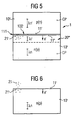
- the Indian FIG. 5 shown body 1 of doped semiconductor material has a uniform crystal body 10 'of doped semiconductor material having a certain mean free path ⁇ n for free charge carriers CP, in a bordering, for example, the upwardly facing surface 11' of the crystal body 10 'region 20'eine for the determined mean free path Xn smaller has a mean free path ⁇ r for the free charge carriers CP.
- the region 20 ' may extend over the entire surface 11' or only over one or more subregions of the surface 11 '. In the direction x perpendicular to the surface 11 of the crystal body 10 ', the region 20' "preferably extends only over part of the crystal body 10 '. In this direction x, the smaller mean free path ⁇ r can vary.
- the crystal body 10 ' Connected to the crystal body 10 'is another uniform crystal body 10 "of doped semiconductor material whose semiconductor material has an average free path An' for the free charge carriers CP which is greater than the smaller mean free path ⁇ r of the crystal body 10 'is.
- the crystal body 10 ' is n-doped and the crystal body 10 "is p-doped, which means that the body 1 after FIG. 5 has a pn junction 100 'between p-doped semiconductor material and n-doped semiconductor material.
- This junction 100 ' extends in the interface between the n-doped crystal body 10 and the p-doped crystal body 10, ie, along the surfaces 11' and 11 "of the crystal bodies 10 'and 10".
- the region 20 '' 'of the smaller mean free path kr is defined by scattering centers 21' in the crystal body 10 which are distributed in the crystal body 10 'and reduce the certain mean free path length k of the semiconductor material of this body 10'.
- the scattering centers 21 ' werdern similar to the body 1 after the FIGS. 2 to 4 and as in the FIG. 6 indicated by introducing non-doping impurity particles 21 into the crystal body 10 'produced by adding non-doping impurity particles 21 during growth of the crystal body 10' of the determined mean free path ⁇ n into the crystal body 10 and / or by diffusing non-doping impurity particles 21 into the crystal body 10 ' ,
- a smaller mean free path ⁇ r varying in the direction x is produced by varying, over time, a quantity of non-doping impurity particles 21 offered to produce scattering centers 21 'in the crystal body 10' during the growth of the crystal body.
- the crystal body 10 'and / or the crystal body 10'' may be thinned by polishing and / or etching steps. Thereafter, if necessary, further method steps which are necessary for the completion of the component can be carried out.
Landscapes
- Recrystallisation Techniques (AREA)
- Crystals, And After-Treatments Of Crystals (AREA)
Applications Claiming Priority (3)
| Application Number | Priority Date | Filing Date | Title |
|---|---|---|---|
| DE10048437A DE10048437A1 (de) | 2000-09-29 | 2000-09-29 | Verfahren zum Herstellen eines Körpers aus Halbleitermaterial mit reduzierter mittlerer freier Weglänge und mit dem Verfahren hergestellter Körper |
| DE10048437 | 2000-09-29 | ||
| PCT/EP2001/009866 WO2002027802A1 (de) | 2000-09-29 | 2001-08-27 | Verfahren zum herstellen eines körpers aus halbleitermaterial mit reduzierter mittlerer freier weglänge |
Publications (2)
| Publication Number | Publication Date |
|---|---|
| EP1320897A1 EP1320897A1 (de) | 2003-06-25 |
| EP1320897B1 true EP1320897B1 (de) | 2012-12-05 |
Family
ID=7658183
Family Applications (1)
| Application Number | Title | Priority Date | Filing Date |
|---|---|---|---|
| EP01985777A Expired - Lifetime EP1320897B1 (de) | 2000-09-29 | 2001-08-27 | Verfahren zum herstellen eines halbleiterbauelements aus halbleitermaterial mit reduzierter mittlerer freier weglänge und mit dem verfahren hergestelltes halbleiterbauelement |
Country Status (6)
| Country | Link |
|---|---|
| US (1) | US9608128B2 (enExample) |
| EP (1) | EP1320897B1 (enExample) |
| JP (2) | JP2004510354A (enExample) |
| KR (1) | KR100898759B1 (enExample) |
| DE (1) | DE10048437A1 (enExample) |
| WO (1) | WO2002027802A1 (enExample) |
Families Citing this family (6)
| Publication number | Priority date | Publication date | Assignee | Title |
|---|---|---|---|---|
| DE10048437A1 (de) | 2000-09-29 | 2002-04-18 | Eupec Gmbh & Co Kg | Verfahren zum Herstellen eines Körpers aus Halbleitermaterial mit reduzierter mittlerer freier Weglänge und mit dem Verfahren hergestellter Körper |
| DE10207339A1 (de) * | 2002-02-21 | 2003-09-11 | Infineon Technologies Ag | Verfahren zur Reduzierung der Beweglichkeit freier Ladungsträger in einem Halbleiterkörper |
| DE102010046215B4 (de) * | 2010-09-21 | 2019-01-03 | Infineon Technologies Austria Ag | Halbleiterkörper mit verspanntem Bereich, Elektronisches Bauelement und ein Verfahren zum Erzeugen des Halbleiterkörpers. |
| CN103700712B (zh) * | 2012-09-27 | 2017-05-03 | 比亚迪股份有限公司 | 一种快恢复二极管的结构及其制造方法 |
| CN104701162A (zh) * | 2013-12-06 | 2015-06-10 | 江苏物联网研究发展中心 | 半导体器件、pin二极管和igbt的制作方法 |
| DE102015111213B4 (de) | 2015-07-10 | 2023-05-04 | Infineon Technologies Ag | Verfahren zum Verringern einer bipolaren Degradation bei einem SiC-Halbleiterbauelement und Halbleiterbauelement |
Citations (3)
| Publication number | Priority date | Publication date | Assignee | Title |
|---|---|---|---|---|
| US4717681A (en) * | 1986-05-19 | 1988-01-05 | Texas Instruments Incorporated | Method of making a heterojunction bipolar transistor with SIPOS |
| US5159429A (en) * | 1990-01-23 | 1992-10-27 | International Business Machines Corporation | Semiconductor device structure employing a multi-level epitaxial structure and method of manufacturing same |
| EP0622834A2 (en) * | 1993-04-30 | 1994-11-02 | International Business Machines Corporation | Method to prevent latch-up and improve breakdown voltage in SOI MOSFETS |
Family Cites Families (17)
| Publication number | Priority date | Publication date | Assignee | Title |
|---|---|---|---|---|
| JP2579979B2 (ja) * | 1987-02-26 | 1997-02-12 | 株式会社東芝 | 半導体素子の製造方法 |
| JPH07107935B2 (ja) * | 1988-02-04 | 1995-11-15 | 株式会社東芝 | 半導体装置 |
| US5102810A (en) * | 1990-03-13 | 1992-04-07 | General Instrument Corp. | Method for controlling the switching speed of bipolar power devices |
| DE4223914C2 (de) * | 1992-06-30 | 1996-01-25 | Fraunhofer Ges Forschung | Verfahren zum Herstellen eines vertikalen Leistungsbauelementes mit reduzierter Minoritätsträgerlebensdauer in dessen Driftstrecke |
| JPH07107935A (ja) * | 1993-08-18 | 1995-04-25 | Kaneto Shoji Kk | 豆腐連続自動製造装置 |
| JP3198766B2 (ja) | 1993-12-27 | 2001-08-13 | 日産自動車株式会社 | 電導度変調型トランジスタ |
| JP2979964B2 (ja) * | 1994-07-25 | 1999-11-22 | 株式会社日立製作所 | 半導体装置及びそれを用いたインバータ装置 |
| US6037632A (en) * | 1995-11-06 | 2000-03-14 | Kabushiki Kaisha Toshiba | Semiconductor device |
| JP3394383B2 (ja) * | 1996-03-18 | 2003-04-07 | 三菱電機株式会社 | サイリスタの製造方法およびサイリスタ |
| JP2917919B2 (ja) * | 1996-06-20 | 1999-07-12 | 日本電気株式会社 | 半導体基板およびその製造方法、並びに半導体素子 |
| WO1998015010A1 (de) * | 1996-09-30 | 1998-04-09 | Eupec Europäische Gesellschaft Für Leistungshalbleiter Mbh + Co. Kg | Thyristor mit durchbruchbereich |
| US6054369A (en) * | 1997-06-30 | 2000-04-25 | Intersil Corporation | Lifetime control for semiconductor devices |
| TW396628B (en) * | 1997-09-04 | 2000-07-01 | Nat Science Council | Structure and process for SiC single crystal/Si single crystal hetero-junction negative differential resistance |
| JPH1199469A (ja) | 1997-09-30 | 1999-04-13 | Nisshin Steel Co Ltd | 金属管の内面研磨方法 |
| AU5847599A (en) * | 1998-07-29 | 2000-02-21 | Infineon Technologies, Ag | Power semiconductor having a reduced reverse current |
| DE10030381B4 (de) * | 2000-06-21 | 2005-04-14 | eupec Europäische Gesellschaft für Leistungshalbleiter mbH & Co. KG | Leistungshalbleiterbauelement aufweisend einen Körper aus Halbleitermaterial mit Übergang zwischen zueinander entgegengesetzten Leiterfähigkeitstypen |
| DE10048437A1 (de) | 2000-09-29 | 2002-04-18 | Eupec Gmbh & Co Kg | Verfahren zum Herstellen eines Körpers aus Halbleitermaterial mit reduzierter mittlerer freier Weglänge und mit dem Verfahren hergestellter Körper |
-
2000
- 2000-09-29 DE DE10048437A patent/DE10048437A1/de not_active Ceased
-
2001
- 2001-08-27 JP JP2002531498A patent/JP2004510354A/ja active Pending
- 2001-08-27 EP EP01985777A patent/EP1320897B1/de not_active Expired - Lifetime
- 2001-08-27 KR KR1020037004420A patent/KR100898759B1/ko not_active Expired - Fee Related
- 2001-08-27 WO PCT/EP2001/009866 patent/WO2002027802A1/de not_active Ceased
-
2003
- 2003-03-20 US US10/392,509 patent/US9608128B2/en not_active Expired - Fee Related
-
2010
- 2010-11-02 JP JP2010246899A patent/JP5566260B2/ja not_active Expired - Fee Related
Patent Citations (3)
| Publication number | Priority date | Publication date | Assignee | Title |
|---|---|---|---|---|
| US4717681A (en) * | 1986-05-19 | 1988-01-05 | Texas Instruments Incorporated | Method of making a heterojunction bipolar transistor with SIPOS |
| US5159429A (en) * | 1990-01-23 | 1992-10-27 | International Business Machines Corporation | Semiconductor device structure employing a multi-level epitaxial structure and method of manufacturing same |
| EP0622834A2 (en) * | 1993-04-30 | 1994-11-02 | International Business Machines Corporation | Method to prevent latch-up and improve breakdown voltage in SOI MOSFETS |
Non-Patent Citations (3)
| Title |
|---|
| ANG S S ET AL: "Growth and characterization of germanium and boron doped silicon epitaxial films", JOURNAL OF ELECTRONIC MATERIALS, WARRENDALE, PA, US, vol. 17, no. 1, 1 January 1988 (1988-01-01), pages 39 - 43, XP009096440, ISSN: 0361-5235, DOI: 10.1007/BF02652231 * |
| KOLA R R ET AL: "Defect and dopant control during silicon epitaxy using B and Ge", DEFECTS IN ELECTRONIC MATERIALS. SYMPOSIUM, 30 NOV.-3 DEC. 1987, BOSTON, MA, USA, 30 November 1987 (1987-11-30) - 3 December 1987 (1987-12-03), Pittsburgh, PA, USA, pages 641 - 644, XP009096435, ISBN: 0-931837-72-3 * |
| QUEIROLO G.; POLIGNANO M.L.: "Incremental sheet resistance and spreading resistance: a comparison", JOURNAL OF VACUUM SCIENCE & TECHNOLOGY B (MICROELECTRONICS PROCESSING AND PHENOMENA), vol. 10, no. 1, 1992, USA, pages 408 - 412 * |
Also Published As
| Publication number | Publication date |
|---|---|
| WO2002027802A1 (de) | 2002-04-04 |
| US20030154912A1 (en) | 2003-08-21 |
| KR100898759B1 (ko) | 2009-05-25 |
| JP2011061226A (ja) | 2011-03-24 |
| KR20030070887A (ko) | 2003-09-02 |
| US9608128B2 (en) | 2017-03-28 |
| EP1320897A1 (de) | 2003-06-25 |
| JP2004510354A (ja) | 2004-04-02 |
| JP5566260B2 (ja) | 2014-08-06 |
| DE10048437A1 (de) | 2002-04-18 |
Similar Documents
| Publication | Publication Date | Title |
|---|---|---|
| DE69631664T2 (de) | SiC-HALBLEITERANORDNUNG MIT EINEM PN-ÜBERGANG, DER EINEN RAND ZUR ABSORPTION DER SPANNUNG ENTHÄLT | |
| EP1056137B1 (de) | Solarzelle mit einer Schutzdiode und ihr Herstellungsverfahren | |
| DE69601981T2 (de) | Herstellungsverfahren einer halbleiteranordnung aus siliziumkarbid | |
| DE102015208097B4 (de) | Herstellen einer Halbleitervorrichtung durch Epitaxie | |
| DE2711562C3 (de) | Halbleiterbauelement und Verfahren zu seiner Herstellung | |
| DE10207522B4 (de) | Halbleiterbauelement und Verfahren zu dessen Herstellung | |
| DE69324074T2 (de) | Verfahren zur Bildung von Kurzschlussgebieten für Halbleiterbauelemente mit isoliertem Gatter | |
| DE60033252T2 (de) | Mehrschichtige halbleiter-struktur mit phosphid-passiviertem germanium-substrat | |
| DE102014103325B4 (de) | Leistungsschaltmodule mit verringerter Oszillation und Verfahren zur Herstellung eines Leistungsschaltmoduls | |
| DE4025269A1 (de) | Elektronisches bauelement und verfahren zu dessen herstellung | |
| EP0557318B1 (de) | Verfahren zur herstellung von halbleiterelementen, insbesondere von dioden | |
| DE2608562A1 (de) | Halbleiteranordnung zum erzeugen inkohaerenter strahlung und verfahren zu deren herstellung | |
| EP1320897B1 (de) | Verfahren zum herstellen eines halbleiterbauelements aus halbleitermaterial mit reduzierter mittlerer freier weglänge und mit dem verfahren hergestelltes halbleiterbauelement | |
| DE2364752A1 (de) | Halbleitervorrichtung | |
| DE3328521C2 (de) | Gleichrichterdiode für hohe Sperrspannung | |
| DE3685842T2 (de) | Verfahren zur herstellung eines ohmischen kontaktes auf einem iii-v halbleiter und hergestelltes halbleiterzwischenprodukt. | |
| DE10015884A1 (de) | Schottky-Diode | |
| DE3851175T2 (de) | Bipolartransistor mit Heteroübergängen. | |
| DE2061689B2 (de) | Tunnel-laufzeitdiode mit schottky- kontakt | |
| DE2044863A1 (de) | Verfahren zur Herstellung von Schottkydioden | |
| DE69319465T2 (de) | Gate-Turn-Off-Thyristor und dessen Verwendung in Leistungwandlern | |
| DE2507038C3 (de) | Inverser Planartransistor und Verfahren zu seiner Herstellung | |
| DE102011081983A1 (de) | Solarzelle und Verfahren zu ihrer Herstellung | |
| DE3644253A1 (de) | Integrierte schottky-diode | |
| DE2620980C2 (enExample) |
Legal Events
| Date | Code | Title | Description |
|---|---|---|---|
| PUAI | Public reference made under article 153(3) epc to a published international application that has entered the european phase |
Free format text: ORIGINAL CODE: 0009012 |
|
| 17P | Request for examination filed |
Effective date: 20030214 |
|
| AK | Designated contracting states |
Designated state(s): AT BE CH CY DE DK ES FI FR GB GR IE IT LI LU MC NL PT SE TR |
|
| RBV | Designated contracting states (corrected) |
Designated state(s): AT BE CH CY DE FR GB IE LI |
|
| RAP1 | Party data changed (applicant data changed or rights of an application transferred) |
Owner name: INFINEON TECHNOLOGIES AG |
|
| 17Q | First examination report despatched |
Effective date: 20060808 |
|
| RAP1 | Party data changed (applicant data changed or rights of an application transferred) |
Owner name: INFINEON TECHNOLOGIES AG |
|
| RTI1 | Title (correction) |
Free format text: METHOD FOR PRODUCING A SEMICONDUCTOR DEVICE CONSISTING OF SEMICONDUCTOR MATERIAL HAVING A REDUCED MEAN FREE PATH LENGTH AND SEMICONDUCTOR DEVICE FABRICATED THEREBY |
|
| GRAJ | Information related to disapproval of communication of intention to grant by the applicant or resumption of examination proceedings by the epo deleted |
Free format text: ORIGINAL CODE: EPIDOSDIGR1 |
|
| GRAP | Despatch of communication of intention to grant a patent |
Free format text: ORIGINAL CODE: EPIDOSNIGR1 |
|
| RBV | Designated contracting states (corrected) |
Designated state(s): DE FR GB IE |
|
| GRAS | Grant fee paid |
Free format text: ORIGINAL CODE: EPIDOSNIGR3 |
|
| GRAA | (expected) grant |
Free format text: ORIGINAL CODE: 0009210 |
|
| AK | Designated contracting states |
Kind code of ref document: B1 Designated state(s): DE FR GB IE |
|
| REG | Reference to a national code |
Ref country code: GB Ref legal event code: FG4D Free format text: NOT ENGLISH |
|
| REG | Reference to a national code |
Ref country code: IE Ref legal event code: FG4D Free format text: LANGUAGE OF EP DOCUMENT: GERMAN |
|
| REG | Reference to a national code |
Ref country code: DE Ref legal event code: R096 Ref document number: 50116212 Country of ref document: DE Effective date: 20130131 |
|
| PLBE | No opposition filed within time limit |
Free format text: ORIGINAL CODE: 0009261 |
|
| STAA | Information on the status of an ep patent application or granted ep patent |
Free format text: STATUS: NO OPPOSITION FILED WITHIN TIME LIMIT |
|
| 26N | No opposition filed |
Effective date: 20130906 |
|
| REG | Reference to a national code |
Ref country code: DE Ref legal event code: R097 Ref document number: 50116212 Country of ref document: DE Effective date: 20130906 |
|
| REG | Reference to a national code |
Ref country code: IE Ref legal event code: MM4A |
|
| PG25 | Lapsed in a contracting state [announced via postgrant information from national office to epo] |
Ref country code: IE Free format text: LAPSE BECAUSE OF NON-PAYMENT OF DUE FEES Effective date: 20130827 |
|
| REG | Reference to a national code |
Ref country code: FR Ref legal event code: PLFP Year of fee payment: 16 |
|
| REG | Reference to a national code |
Ref country code: FR Ref legal event code: PLFP Year of fee payment: 17 |
|
| REG | Reference to a national code |
Ref country code: FR Ref legal event code: PLFP Year of fee payment: 18 |
|
| PGFP | Annual fee paid to national office [announced via postgrant information from national office to epo] |
Ref country code: FR Payment date: 20180827 Year of fee payment: 18 |
|
| PGFP | Annual fee paid to national office [announced via postgrant information from national office to epo] |
Ref country code: GB Payment date: 20180822 Year of fee payment: 18 |
|
| PGFP | Annual fee paid to national office [announced via postgrant information from national office to epo] |
Ref country code: DE Payment date: 20181029 Year of fee payment: 18 |
|
| REG | Reference to a national code |
Ref country code: DE Ref legal event code: R119 Ref document number: 50116212 Country of ref document: DE |
|
| GBPC | Gb: european patent ceased through non-payment of renewal fee |
Effective date: 20190827 |
|
| PG25 | Lapsed in a contracting state [announced via postgrant information from national office to epo] |
Ref country code: DE Free format text: LAPSE BECAUSE OF NON-PAYMENT OF DUE FEES Effective date: 20200303 Ref country code: FR Free format text: LAPSE BECAUSE OF NON-PAYMENT OF DUE FEES Effective date: 20190831 |
|
| PG25 | Lapsed in a contracting state [announced via postgrant information from national office to epo] |
Ref country code: GB Free format text: LAPSE BECAUSE OF NON-PAYMENT OF DUE FEES Effective date: 20190827 |