EP0622834A2 - Method to prevent latch-up and improve breakdown voltage in SOI MOSFETS - Google Patents
Method to prevent latch-up and improve breakdown voltage in SOI MOSFETS Download PDFInfo
- Publication number
- EP0622834A2 EP0622834A2 EP94102414A EP94102414A EP0622834A2 EP 0622834 A2 EP0622834 A2 EP 0622834A2 EP 94102414 A EP94102414 A EP 94102414A EP 94102414 A EP94102414 A EP 94102414A EP 0622834 A2 EP0622834 A2 EP 0622834A2
- Authority
- EP
- European Patent Office
- Prior art keywords
- substrate
- soi
- silicon
- germanium
- devices
- Prior art date
- Legal status (The legal status is an assumption and is not a legal conclusion. Google has not performed a legal analysis and makes no representation as to the accuracy of the status listed.)
- Ceased
Links
- 238000000034 method Methods 0.000 title claims abstract description 23
- 230000015556 catabolic process Effects 0.000 title claims abstract description 7
- 239000007943 implant Substances 0.000 claims abstract description 20
- 230000007935 neutral effect Effects 0.000 claims abstract description 18
- 229910052732 germanium Inorganic materials 0.000 claims abstract description 11
- GNPVGFCGXDBREM-UHFFFAOYSA-N germanium atom Chemical compound [Ge] GNPVGFCGXDBREM-UHFFFAOYSA-N 0.000 claims abstract description 11
- 229910052710 silicon Inorganic materials 0.000 claims abstract description 8
- 230000003071 parasitic effect Effects 0.000 claims abstract description 6
- 239000010703 silicon Substances 0.000 claims abstract description 6
- 229910052743 krypton Inorganic materials 0.000 claims abstract description 5
- DNNSSWSSYDEUBZ-UHFFFAOYSA-N krypton atom Chemical compound [Kr] DNNSSWSSYDEUBZ-UHFFFAOYSA-N 0.000 claims abstract description 5
- 239000012212 insulator Substances 0.000 claims abstract description 3
- 239000000758 substrate Substances 0.000 claims description 14
- 238000002513 implantation Methods 0.000 claims description 9
- 239000004065 semiconductor Substances 0.000 claims description 5
- 230000015572 biosynthetic process Effects 0.000 claims description 2
- 238000004519 manufacturing process Methods 0.000 claims description 2
- XKRFYHLGVUSROY-UHFFFAOYSA-N Argon Chemical compound [Ar] XKRFYHLGVUSROY-UHFFFAOYSA-N 0.000 claims 4
- 229910052786 argon Inorganic materials 0.000 claims 2
- 239000004020 conductor Substances 0.000 claims 2
- 238000013459 approach Methods 0.000 abstract description 15
- 239000012535 impurity Substances 0.000 abstract description 14
- XUIMIQQOPSSXEZ-UHFFFAOYSA-N Silicon Chemical compound [Si] XUIMIQQOPSSXEZ-UHFFFAOYSA-N 0.000 abstract description 7
- 230000000694 effects Effects 0.000 abstract description 5
- 238000005516 engineering process Methods 0.000 abstract description 4
- 229910052724 xenon Inorganic materials 0.000 abstract description 3
- FHNFHKCVQCLJFQ-UHFFFAOYSA-N xenon atom Chemical compound [Xe] FHNFHKCVQCLJFQ-UHFFFAOYSA-N 0.000 abstract description 3
- 230000005855 radiation Effects 0.000 abstract description 2
- 238000004969 ion scattering spectroscopy Methods 0.000 abstract 1
- 239000000969 carrier Substances 0.000 description 15
- 230000007423 decrease Effects 0.000 description 5
- 235000012431 wafers Nutrition 0.000 description 4
- 230000005684 electric field Effects 0.000 description 3
- 230000009024 positive feedback mechanism Effects 0.000 description 3
- 208000032750 Device leakage Diseases 0.000 description 2
- 238000013461 design Methods 0.000 description 2
- 239000002019 doping agent Substances 0.000 description 2
- 238000005215 recombination Methods 0.000 description 2
- 230000006798 recombination Effects 0.000 description 2
- 125000006850 spacer group Chemical group 0.000 description 2
- 210000000746 body region Anatomy 0.000 description 1
- 239000003031 high energy carrier Substances 0.000 description 1
- 230000004941 influx Effects 0.000 description 1
- 150000002500 ions Chemical class 0.000 description 1
- 238000002955 isolation Methods 0.000 description 1
- 238000005259 measurement Methods 0.000 description 1
- 230000002265 prevention Effects 0.000 description 1
- 238000012545 processing Methods 0.000 description 1
Images


Classifications
-
- H—ELECTRICITY
- H01—ELECTRIC ELEMENTS
- H01L—SEMICONDUCTOR DEVICES NOT COVERED BY CLASS H10
- H01L21/00—Processes or apparatus adapted for the manufacture or treatment of semiconductor or solid state devices or of parts thereof
- H01L21/02—Manufacture or treatment of semiconductor devices or of parts thereof
- H01L21/04—Manufacture or treatment of semiconductor devices or of parts thereof the devices having at least one potential-jump barrier or surface barrier, e.g. PN junction, depletion layer or carrier concentration layer
- H01L21/18—Manufacture or treatment of semiconductor devices or of parts thereof the devices having at least one potential-jump barrier or surface barrier, e.g. PN junction, depletion layer or carrier concentration layer the devices having semiconductor bodies comprising elements of Group IV of the Periodic System or AIIIBV compounds with or without impurities, e.g. doping materials
- H01L21/26—Bombardment with radiation
- H01L21/263—Bombardment with radiation with high-energy radiation
- H01L21/265—Bombardment with radiation with high-energy radiation producing ion implantation
- H01L21/26506—Bombardment with radiation with high-energy radiation producing ion implantation in group IV semiconductors
-
- H—ELECTRICITY
- H01—ELECTRIC ELEMENTS
- H01L—SEMICONDUCTOR DEVICES NOT COVERED BY CLASS H10
- H01L29/00—Semiconductor devices adapted for rectifying, amplifying, oscillating or switching, or capacitors or resistors with at least one potential-jump barrier or surface barrier, e.g. PN junction depletion layer or carrier concentration layer; Details of semiconductor bodies or of electrodes thereof ; Multistep manufacturing processes therefor
- H01L29/66—Types of semiconductor device ; Multistep manufacturing processes therefor
- H01L29/66007—Multistep manufacturing processes
- H01L29/66075—Multistep manufacturing processes of devices having semiconductor bodies comprising group 14 or group 13/15 materials
- H01L29/66227—Multistep manufacturing processes of devices having semiconductor bodies comprising group 14 or group 13/15 materials the devices being controllable only by the electric current supplied or the electric potential applied, to an electrode which does not carry the current to be rectified, amplified or switched, e.g. three-terminal devices
- H01L29/66409—Unipolar field-effect transistors
- H01L29/66477—Unipolar field-effect transistors with an insulated gate, i.e. MISFET
- H01L29/66742—Thin film unipolar transistors
- H01L29/66772—Monocristalline silicon transistors on insulating substrates, e.g. quartz substrates
-
- H—ELECTRICITY
- H01—ELECTRIC ELEMENTS
- H01L—SEMICONDUCTOR DEVICES NOT COVERED BY CLASS H10
- H01L29/00—Semiconductor devices adapted for rectifying, amplifying, oscillating or switching, or capacitors or resistors with at least one potential-jump barrier or surface barrier, e.g. PN junction depletion layer or carrier concentration layer; Details of semiconductor bodies or of electrodes thereof ; Multistep manufacturing processes therefor
- H01L29/66—Types of semiconductor device ; Multistep manufacturing processes therefor
- H01L29/68—Types of semiconductor device ; Multistep manufacturing processes therefor controllable by only the electric current supplied, or only the electric potential applied, to an electrode which does not carry the current to be rectified, amplified or switched
- H01L29/76—Unipolar devices, e.g. field effect transistors
- H01L29/772—Field effect transistors
- H01L29/78—Field effect transistors with field effect produced by an insulated gate
- H01L29/786—Thin film transistors, i.e. transistors with a channel being at least partly a thin film
- H01L29/78606—Thin film transistors, i.e. transistors with a channel being at least partly a thin film with supplementary region or layer in the thin film or in the insulated bulk substrate supporting it for controlling or increasing the safety of the device
- H01L29/78612—Thin film transistors, i.e. transistors with a channel being at least partly a thin film with supplementary region or layer in the thin film or in the insulated bulk substrate supporting it for controlling or increasing the safety of the device for preventing the kink- or the snapback effect, e.g. discharging the minority carriers of the channel region for preventing bipolar effect
-
- Y—GENERAL TAGGING OF NEW TECHNOLOGICAL DEVELOPMENTS; GENERAL TAGGING OF CROSS-SECTIONAL TECHNOLOGIES SPANNING OVER SEVERAL SECTIONS OF THE IPC; TECHNICAL SUBJECTS COVERED BY FORMER USPC CROSS-REFERENCE ART COLLECTIONS [XRACs] AND DIGESTS
- Y10—TECHNICAL SUBJECTS COVERED BY FORMER USPC
- Y10S—TECHNICAL SUBJECTS COVERED BY FORMER USPC CROSS-REFERENCE ART COLLECTIONS [XRACs] AND DIGESTS
- Y10S148/00—Metal treatment
- Y10S148/04—Dopants, special
Definitions
- This invention relates to semiconductor device processing, and more particularly, to latch-up prevention and increased breakdown voltage in SOI devices.
- SOI silicon-on-insulator
- SOI silicon-on-insulator
- one of the disadvantages of SOI devices is the parasitic bipolar induced latch-up/breakdown voltage, which severely limits the maximum power supply voltage at which SOI circuits and devices can operate.
- the parasitic device turns on, the SOI device cannot be switched off by changing its gate bias. This single transistor latch-up also manifests itself as a very low breakdown voltage.
- the SOI device self latch-up effect is caused by a positive feedback mechanism generated by the steady-state balancing between the minority and majority carriers in the body of the transistor.
- the electric field at the body/drain junction becomes high enough so that electron/hole pairs are generated by impact ionization.
- the majority carriers carriers of the same dopant type as the source and drain
- the body of the transistor is separated from the substrate by a buried oxide.
- the minority carriers thus collect in the body of the transistor.
- the concentration of minority carriers in the body disturbs the normal steady state potential of the body.
- majority carriers are injected from the source. These carriers then diffuse to the high field region of the drain/body junction, creating even more electron/hole pairs by impact ionization, and cause a run-away current in the device.
- body tie In the body tie approach, either an extra contact is attached to the body of the transistor to keep the voltage potential from floating, or highly doped straps are used to short the body to the source.
- body ties are useful only for thick-film SOI devices. As the film becomes thinner, the sheet resistance of the body increases, and the body tie collects a lower percentage of the excess current. As a result, extra ties/straps are needed, greatly increasing the required device area.
- implementing body ties requires significant design changes from bulk silicon transistor technology. Thus, circuits implementing body ties must be designed for SOI from the start, thereby increasing cost.
- the LDD approach aims to decrease the electric field at the body/drain junction by reducing the dopant gradient (from the very highly doped drain to the low doped body) in this region. This is accomplished by the use of a spacer to explicitly separate the drain from the body. An additional implant is used to decrease the resistance of the spacer region. This approach can be used to easily increase the operating voltage.
- the generation lifetime refers to the generation of carriers by thermal effects. Thermally generated carriers contribute to the off-state device leakage. As devices are made with shorter gates, shorter recombination lifetimes are required to increase the maximum drain voltage. However, the generation lifetime decreases proportionally, so that the submicron devices would be excessively leaky. In addition, the minimum acceptable leakage decreases as devices are shrunk.
- the present invention is a method to improve the device operating voltage via implantation of neutral impurity ions into the silicon transistor devices.
- the implants are used to generate scattering centers in the high field region of the drain/body junction. These scattering centers reduce the mean free path of electrons, thus reducing the energy they acquire. Since the carriers have less energy, less impact ionization occurs.
- the neutral impurities include group VIII atoms such as Krypton and Xenon. Germanium may also be used, since it is electrically neutral in silicon. It is key that the size of the impurity atom be much larger then the size of the silicon atom. The size difference generates the scattering.
- the present invention employs neutral impurities to generate scattering centers in the high field region of a transistor.
- Neutral impurities include group VIII atoms such as krypton and xenon and also germanium. Because of the increased size of these atoms and with the disturbance in the band structure, high energy carriers within the transistor see more scattering centers. The amount of energy that an electron or hole accumulates in a high field region depends upon how far it travels before it encounters a scattering center. Thus, for a given drain field having neutral impurity centers the impact ionization current is reduced, this reducing the parasitic bipolar effects.
- a typical SOI device is shown in Figure 1 wherein the device 10 has a substrate 12, an insulating buried oxide 14, a drain and source region 16 and 18 respectively, a gate oxide 20, and a gate electrode 22.
- the body region 24 is the channel region under the gate between the source and drain regions of the device.
- the process prescribes the implantation of a neutral species followed by an anneal to eliminate implant induced damage.
- the implant can be done at several different points in the process. For example, the implant can be done after the formation of the lateral isolation (through a dummy gate oxide), or after the definition of the gate.
- This invention was demonstrated by the implantation of germanium.
- the optimum energy for the implantation depends in part whether the transistor is a surface channel or buried channel device. However, an implant energy window exists, below which one excessively damages the surface and above which one amorphizes the film. In the sent process an energy of 60 KeV was used.
- the implant dose should be in the order of 1E14 to 1E16 cm-2 range.
- the anneal should be at a temperature of approximately 900 °C for at least 30 minutes to remove the implant damage and to avoid leaky transistor characteristics.
- the present invention avoids the problems of the approaches described in the background art.
- the neutral impurity implant approach is compatible with bulk designs.
- the neutral impurity implant process is very simple and does not degrade device performance.
- the present method does not increase the device leakage currents.
- the inventive process was implemented using a germanium implantation.
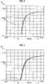
- the drain current versus gate voltage I-V characteristics for an SOI device without the neutrality impurity implant is shown in Figure 2. It is seen that at a drain bias of around 3 volts the gate begins to lose control of the device current (self latch-up begins). For a device of the same dimensions processed identically except for the neutral impurity implant, self latch-up occurs at about 4 volts as seen in Figure 3. Additional results are shown in Figure 4 in which the latch-up voltage was measured for both n and p-channel devices on two device wafers, with and without the neutral impurity implant.
- the germanium implant was applied to a single lot of wafers with one half of the wafers being implanted and the other half being without neutral impurity implantation. Measurements were taken on 147 devices. The use of the implant was seen to improve latch-up on an average of 1.04 volts.
Landscapes
- Engineering & Computer Science (AREA)
- Power Engineering (AREA)
- Microelectronics & Electronic Packaging (AREA)
- Physics & Mathematics (AREA)
- General Physics & Mathematics (AREA)
- Condensed Matter Physics & Semiconductors (AREA)
- Computer Hardware Design (AREA)
- Manufacturing & Machinery (AREA)
- High Energy & Nuclear Physics (AREA)
- Ceramic Engineering (AREA)
- Toxicology (AREA)
- Health & Medical Sciences (AREA)
- Thin Film Transistor (AREA)
- Metal-Oxide And Bipolar Metal-Oxide Semiconductor Integrated Circuits (AREA)
Abstract
Description
- This invention relates to semiconductor device processing, and more particularly, to latch-up prevention and increased breakdown voltage in SOI devices.
- Circuits and devices built in SOI substrates have been shown to have many advantages over identical circuits built in bulk silicon substrates. SOI (silicon-on-insulator) technology has been touted as a promising approach for fabricating advanced integrated circuits because of its faster speed and improved radiation tolerance. However, one of the disadvantages of SOI devices is the parasitic bipolar induced latch-up/breakdown voltage, which severely limits the maximum power supply voltage at which SOI circuits and devices can operate. When the parasitic device turns on, the SOI device cannot be switched off by changing its gate bias. This single transistor latch-up also manifests itself as a very low breakdown voltage. The SOI device self latch-up effect is caused by a positive feedback mechanism generated by the steady-state balancing between the minority and majority carriers in the body of the transistor. For a given gate voltage, as the drain voltage is increased, the electric field at the body/drain junction becomes high enough so that electron/hole pairs are generated by impact ionization. The majority carriers (carriers of the same dopant type as the source and drain) are collected at the drain while minority carriers travel into the body of the transistor. In SOI devices, the body of the transistor is separated from the substrate by a buried oxide. The minority carriers thus collect in the body of the transistor. At sufficiently high drain bias, the concentration of minority carriers in the body disturbs the normal steady state potential of the body. To compensate, majority carriers are injected from the source. These carriers then diffuse to the high field region of the drain/body junction, creating even more electron/hole pairs by impact ionization, and cause a run-away current in the device.
- Several approaches have been discussed in the known art for increasing the voltage at the drain for onset of the device self latch-up/breakdown effect. The known approaches are based on reducing the drain electric field for a given drain bias (LDD approaches) or adding an extra contact to the body of the transistor to keep it at a constant potential and to act as a sink for the excess carriers (body tie approaches).
- In the body tie approach, either an extra contact is attached to the body of the transistor to keep the voltage potential from floating, or highly doped straps are used to short the body to the source. However, body ties are useful only for thick-film SOI devices. As the film becomes thinner, the sheet resistance of the body increases, and the body tie collects a lower percentage of the excess current. As a result, extra ties/straps are needed, greatly increasing the required device area. In addition, implementing body ties requires significant design changes from bulk silicon transistor technology. Thus, circuits implementing body ties must be designed for SOI from the start, thereby increasing cost.
- The LDD approach aims to decrease the electric field at the body/drain junction by reducing the dopant gradient (from the very highly doped drain to the low doped body) in this region. This is accomplished by the use of a spacer to explicitly separate the drain from the body. An additional implant is used to decrease the resistance of the spacer region. This approach can be used to easily increase the operating voltage.
- However, a price is paid in terms of slower circuit speed. It is difficult to optimize the circuit speed versus the maximum operating voltage. In addition, the LDD process requires many process steps to be added to the transistor fabrication process.
- Another approach is to reduce the lifetime of minority carriers in the transistor body. When carriers quickly recombine, a larger influx of carriers is needed to disturb the body potential sufficiently to induce the positive feedback mechanism. Thus, the voltage at which the positive feedback mechanism occurs is increased. However, it is difficult to decrease the recombination lifetime without increasing the generation lifetime. The generation lifetime refers to the generation of carriers by thermal effects. Thermally generated carriers contribute to the off-state device leakage. As devices are made with shorter gates, shorter recombination lifetimes are required to increase the maximum drain voltage. However, the generation lifetime decreases proportionally, so that the submicron devices would be excessively leaky. In addition, the minimum acceptable leakage decreases as devices are shrunk.
- What is needed is a method whereby the operating voltage at which the latch-up occurs is significantly increased thus allowing circuit operation at reasonable power supply voltages.
- The present invention is a method to improve the device operating voltage via implantation of neutral impurity ions into the silicon transistor devices. The implants are used to generate scattering centers in the high field region of the drain/body junction. These scattering centers reduce the mean free path of electrons, thus reducing the energy they acquire. Since the carriers have less energy, less impact ionization occurs. The neutral impurities include group VIII atoms such as Krypton and Xenon. Germanium may also be used, since it is electrically neutral in silicon. It is key that the size of the impurity atom be much larger then the size of the silicon atom. The size difference generates the scattering.
- The objects, features and advantages of the invention will be fully understood with reference to the description of the preferred embodiment and the drawings wherein:
- Figure 1
- is a cross sectional view of a semiconductor device built in SOI technology.
- Figure 2
- is a graph of the latch-up voltage for a device without the implant.
- Figure 3
- is a latch-up voltage graph of a germanium implanted device according to the present invention.
- Figure 4
- is a comparison of latch-up voltages for transistors with and without a germanium implant.
- The present invention employs neutral impurities to generate scattering centers in the high field region of a transistor. Neutral impurities include group VIII atoms such as krypton and xenon and also germanium. Because of the increased size of these atoms and with the disturbance in the band structure, high energy carriers within the transistor see more scattering centers. The amount of energy that an electron or hole accumulates in a high field region depends upon how far it travels before it encounters a scattering center. Thus, for a given drain field having neutral impurity centers the impact ionization current is reduced, this reducing the parasitic bipolar effects.
- A typical SOI device is shown in Figure 1 wherein the
device 10 has asubstrate 12, an insulating buriedoxide 14, a drain andsource region gate oxide 20, and a gate electrode 22. Thebody region 24 is the channel region under the gate between the source and drain regions of the device. The process prescribes the implantation of a neutral species followed by an anneal to eliminate implant induced damage. The implant can be done at several different points in the process. For example, the implant can be done after the formation of the lateral isolation (through a dummy gate oxide), or after the definition of the gate. - This invention was demonstrated by the implantation of germanium. The optimum energy for the implantation depends in part whether the transistor is a surface channel or buried channel device. However, an implant energy window exists, below which one excessively damages the surface and above which one amorphizes the film. In the sent process an energy of 60 KeV was used. The implant dose should be in the order of 1E14 to 1E16 cm-2 range.
- It is important to follow the implantation by an anneal of the wafer to remove implant induced damage. The anneal should be at a temperature of approximately 900 °C for at least 30 minutes to remove the implant damage and to avoid leaky transistor characteristics.
- The present invention avoids the problems of the approaches described in the background art. For example, unlike the body tie approach, the neutral impurity implant approach is compatible with bulk designs. Again, unlike the LDD approach, the neutral impurity implant process is very simple and does not degrade device performance. Finally, unlike the lifetime killing approach, the present method does not increase the device leakage currents.
- The inventive process was implemented using a germanium implantation. The drain current versus gate voltage I-V characteristics for an SOI device without the neutrality impurity implant is shown in Figure 2. It is seen that at a drain bias of around 3 volts the gate begins to lose control of the device current (self latch-up begins). For a device of the same dimensions processed identically except for the neutral impurity implant, self latch-up occurs at about 4 volts as seen in Figure 3. Additional results are shown in Figure 4 in which the latch-up voltage was measured for both n and p-channel devices on two device wafers, with and without the neutral impurity implant. To further demonstrate the validity of the technique, the germanium implant was applied to a single lot of wafers with one half of the wafers being implanted and the other half being without neutral impurity implantation. Measurements were taken on 147 devices. The use of the implant was seen to improve latch-up on an average of 1.04 volts.
- While the invention has been shown with reference to a preferred embodiment, it would be obvious to ones skilled in the art that the process could be modified and expanded for various species of implantation, energy and dose levels without departing from the spirit of the scope of the invention.
Claims (9)
- A method of fabricating integrated circuits having reduced parasitic latch-up and increase breakdown voltage comprising the steps of:a) providing a semiconductor substrate;b) growing an oxide layer on said substrate;c) blanket implanting the substrate with large diameter neutral atoms;d) forming active devices (10) on said substrate; ande) forming electrical conductors on said substrate to interconnect said devices.
- The method of claim 1, wherein the order of the steps of the blanket implantation and the formation of active devices (10) is reversed.
- The method of claim 1 or 2, wherein the substrate is silicon.
- The method of claim 1 or 2, wherein the substrate is silicon-on-insulator (24, 14).
- The method of one of claims 1 to 4, wherein said integrated circuits are MOSFETs (10).
- The method of one of claims 1 to 5, wherein said large diameter neutral atoms are selected from the group consisting of krypton, argon, and germanium.
- The method of one of claims 1 to 6, wherein said large diameter neutral atom is germanium implanted at 50 to 60 KeV with a dose in the range of 1E14 to 1E16 cm-2.
- In an integrated circuit including a substrate, semiconductor devices formed on said substrate, and electrical conductors interconnecting said semiconductor devices, the improvement comprising the addition of a blanket implant of large diameter neutral atoms into said substrate.
- The method as claimed in claim 8, wherein said neutral atom is selected from the group consisting of krypton, argon, and germanium.
Applications Claiming Priority (2)
| Application Number | Priority Date | Filing Date | Title |
|---|---|---|---|
| US5604293A | 1993-04-30 | 1993-04-30 | |
| US56042 | 1993-04-30 |
Publications (2)
| Publication Number | Publication Date |
|---|---|
| EP0622834A2 true EP0622834A2 (en) | 1994-11-02 |
| EP0622834A3 EP0622834A3 (en) | 1998-02-11 |
Family
ID=22001790
Family Applications (1)
| Application Number | Title | Priority Date | Filing Date |
|---|---|---|---|
| EP94102414A Ceased EP0622834A3 (en) | 1993-04-30 | 1994-02-17 | Method to prevent latch-up and improve breakdown voltage in SOI MOSFETS |
Country Status (3)
| Country | Link |
|---|---|
| US (1) | US5527724A (en) |
| EP (1) | EP0622834A3 (en) |
| JP (1) | JP2891321B2 (en) |
Cited By (4)
| Publication number | Priority date | Publication date | Assignee | Title |
|---|---|---|---|---|
| EP0735592A2 (en) * | 1995-03-31 | 1996-10-02 | Nippon Telegraph And Telephone Corporation | MOS thin film transistor and method of fabricating the same |
| US5585286A (en) * | 1995-08-31 | 1996-12-17 | Lsi Logic Corporation | Implantation of a semiconductor substrate with controlled amount of noble gas ions to reduce channeling and/or diffusion of a boron dopant subsequently implanted into the substrate to form P- LDD region of a PMOS device |
| US6657241B1 (en) | 1998-04-10 | 2003-12-02 | Cypress Semiconductor Corp. | ESD structure having an improved noise immunity in CMOS and BICMOS semiconductor devices |
| EP1320897B1 (en) * | 2000-09-29 | 2012-12-05 | Infineon Technologies AG | Method for producing a semiconductor device consisting of semiconductor material having a reduced mean free path length and semiconductor device fabricated thereby |
Families Citing this family (24)
| Publication number | Priority date | Publication date | Assignee | Title |
|---|---|---|---|---|
| US5514902A (en) * | 1993-09-16 | 1996-05-07 | Mitsubishi Denki Kabushiki Kaisha | Semiconductor device having MOS transistor |
| JP3361922B2 (en) * | 1994-09-13 | 2003-01-07 | 株式会社東芝 | Semiconductor device |
| US5985703A (en) | 1994-10-24 | 1999-11-16 | Banerjee; Sanjay | Method of making thin film transistors |
| US5773328A (en) * | 1995-02-28 | 1998-06-30 | Sgs-Thomson Microelectronics, Inc. | Method of making a fully-dielectric-isolated fet |
| US5985728A (en) * | 1995-09-01 | 1999-11-16 | Elantec Semiconductor, Inc. | Silicon on insulator process with recovery of a device layer from an etch stop layer |
| US5789310A (en) * | 1996-12-10 | 1998-08-04 | Advanced Micro Devices, Inc. | Method of forming shallow junctions by entrapment of interstitial atoms |
| US6337500B1 (en) | 1997-06-19 | 2002-01-08 | Matsushita Electric Industrial Co., Ltd. | Semiconductor device and method for fabricating the same |
| US5915199A (en) * | 1998-06-04 | 1999-06-22 | Sharp Microelectronics Technology, Inc. | Method for manufacturing a CMOS self-aligned strapped interconnection |
| US6482725B1 (en) | 1999-08-18 | 2002-11-19 | Advanced Micro Devices, Inc. | Gate formation method for reduced poly-depletion and boron penetration |
| US6633066B1 (en) * | 2000-01-07 | 2003-10-14 | Samsung Electronics Co., Ltd. | CMOS integrated circuit devices and substrates having unstrained silicon active layers |
| JP3504212B2 (en) | 2000-04-04 | 2004-03-08 | シャープ株式会社 | Semiconductor device with SOI structure |
| US6495887B1 (en) | 2000-06-09 | 2002-12-17 | Advanced Micro Devices, Inc. | Argon implantation after silicidation for improved floating-body effects |
| DE10030381B4 (en) * | 2000-06-21 | 2005-04-14 | eupec Europäische Gesellschaft für Leistungshalbleiter mbH & Co. KG | Power semiconductor device comprising a body of semiconductor material with transition between mutually opposite conductivity types |
| DE10048345A1 (en) * | 2000-09-29 | 2002-05-16 | Eupec Gmbh & Co Kg | Bodies made of semiconductor material with a reduced mean free path |
| US6638832B2 (en) | 2000-12-21 | 2003-10-28 | Bae Systems Information And Electronic Systems Integration, Inc. | Elimination of narrow device width effects in complementary metal oxide semiconductor (CMOS) devices |
| US6509613B1 (en) * | 2001-05-04 | 2003-01-21 | Advanced Micro Devices, Inc. | Self-aligned floating body control for SOI device through leakage enhanced buried oxide |
| US7122863B1 (en) | 2001-05-07 | 2006-10-17 | Advanced Micro Devices, Inc. | SOI device with structure for enhancing carrier recombination and method of fabricating same |
| US6624037B2 (en) * | 2001-08-01 | 2003-09-23 | Advanced Micro Devices, Inc. | XE preamorphizing implantation |
| US6506654B1 (en) * | 2002-03-26 | 2003-01-14 | Advanced Micro Devices, Inc. | Source-side stacking fault body-tie for partially-depleted SOI MOSFET hysteresis control |
| JP3873012B2 (en) * | 2002-07-29 | 2007-01-24 | 株式会社東芝 | Manufacturing method of semiconductor device |
| US6803270B2 (en) * | 2003-02-21 | 2004-10-12 | International Business Machines Corporation | CMOS performance enhancement using localized voids and extended defects |
| CN100416839C (en) * | 2003-10-13 | 2008-09-03 | 联华电子股份有限公司 | Portion lacked SOI VMOS element |
| US20050090067A1 (en) * | 2003-10-27 | 2005-04-28 | Dharmesh Jawarani | Silicide formation for a semiconductor device |
| US8748285B2 (en) | 2011-11-28 | 2014-06-10 | International Business Machines Corporation | Noble gas implantation region in top silicon layer of semiconductor-on-insulator substrate |
Citations (4)
| Publication number | Priority date | Publication date | Assignee | Title |
|---|---|---|---|---|
| JPH01235276A (en) * | 1988-03-15 | 1989-09-20 | Sony Corp | Thin film semiconductor device |
| EP0419128A1 (en) * | 1989-09-22 | 1991-03-27 | AT&T Corp. | Silicon MOSFET doped with germanium to increase lifetime of operation |
| JPH04313242A (en) * | 1991-04-10 | 1992-11-05 | Sony Corp | Manufacture of thin-film semiconductor device |
| JPH04367219A (en) * | 1991-06-14 | 1992-12-18 | Canon Inc | Semiconductor element and its manufacture |
Family Cites Families (11)
| Publication number | Priority date | Publication date | Assignee | Title |
|---|---|---|---|---|
| US4160984A (en) * | 1977-11-14 | 1979-07-10 | Hughes Aircraft Company | Schottky-gate field-effect transistor and fabrication process therefor |
| JPS5891682A (en) * | 1981-11-27 | 1983-05-31 | Hitachi Ltd | Semiconductor device |
| JPS60246195A (en) * | 1984-05-22 | 1985-12-05 | Fuji Photo Film Co Ltd | Recording and reproducing system of line sequential video signal |
| US4603471A (en) * | 1984-09-06 | 1986-08-05 | Fairchild Semiconductor Corporation | Method for making a CMOS circuit having a reduced tendency to latch by controlling the band-gap of source and drain regions |
| US4634473A (en) * | 1985-09-09 | 1987-01-06 | Rca Corporation | Method for fabricating a radiation hardened oxide having structural damage |
| US4946735A (en) * | 1986-02-10 | 1990-08-07 | Cornell Research Foundation, Inc. | Ultra-thin semiconductor membranes |
| US4766482A (en) * | 1986-12-09 | 1988-08-23 | General Electric Company | Semiconductor device and method of making the same |
| US5053353A (en) * | 1988-11-21 | 1991-10-01 | Harris Corporation | Fabricating dielectric isolation of SOI island side wall for reducing leakage current |
| US5102810A (en) * | 1990-03-13 | 1992-04-07 | General Instrument Corp. | Method for controlling the switching speed of bipolar power devices |
| US5156994A (en) * | 1990-12-21 | 1992-10-20 | Texas Instruments Incorporated | Local interconnect method and structure |
| JPH04337625A (en) * | 1991-05-15 | 1992-11-25 | Kawasaki Steel Corp | Semiconductor device fabricating method |
-
1994
- 1994-02-17 EP EP94102414A patent/EP0622834A3/en not_active Ceased
- 1994-04-18 JP JP6078654A patent/JP2891321B2/en not_active Expired - Lifetime
- 1994-09-12 US US08/304,639 patent/US5527724A/en not_active Expired - Lifetime
Patent Citations (4)
| Publication number | Priority date | Publication date | Assignee | Title |
|---|---|---|---|---|
| JPH01235276A (en) * | 1988-03-15 | 1989-09-20 | Sony Corp | Thin film semiconductor device |
| EP0419128A1 (en) * | 1989-09-22 | 1991-03-27 | AT&T Corp. | Silicon MOSFET doped with germanium to increase lifetime of operation |
| JPH04313242A (en) * | 1991-04-10 | 1992-11-05 | Sony Corp | Manufacture of thin-film semiconductor device |
| JPH04367219A (en) * | 1991-06-14 | 1992-12-18 | Canon Inc | Semiconductor element and its manufacture |
Non-Patent Citations (4)
| Title |
|---|
| PATENT ABSTRACTS OF JAPAN vol. 013, no. 564 (E-860), 14 December 1989 -& JP 01 235276 A (SONY CORP), 20 September 1989, * |
| PATENT ABSTRACTS OF JAPAN vol. 017, no. 148 (E-1338), 24 March 1993 -& JP 04 313242 A (SONY CORP), 5 November 1992, * |
| PATENT ABSTRACTS OF JAPAN vol. 017, no. 241 (E-1364), 14 May 1993 -& JP 04 367219 A (CANON INC), 18 December 1992, * |
| WEI H F ET AL: "IMPROVEMENT OF BREAKDOWN VOLTAGE AND OFF-STATE LEAKAGE IN GE-IMPLANTED SOI N-MOSFETS" PROCEEDINGS OF THE INTERNATIONAL ELECTRON DEVICES MEETING, WASHINGTON, DEC. 5 - 8, 1993, 5 December 1993, INSTITUTE OF ELECTRICAL AND ELECTRONICS ENGINEERS, pages 739-742, XP000481719 * |
Cited By (6)
| Publication number | Priority date | Publication date | Assignee | Title |
|---|---|---|---|---|
| EP0735592A2 (en) * | 1995-03-31 | 1996-10-02 | Nippon Telegraph And Telephone Corporation | MOS thin film transistor and method of fabricating the same |
| EP0735592A3 (en) * | 1995-03-31 | 1997-11-05 | Nippon Telegraph And Telephone Corporation | MOS thin film transistor and method of fabricating the same |
| US5585286A (en) * | 1995-08-31 | 1996-12-17 | Lsi Logic Corporation | Implantation of a semiconductor substrate with controlled amount of noble gas ions to reduce channeling and/or diffusion of a boron dopant subsequently implanted into the substrate to form P- LDD region of a PMOS device |
| US6657241B1 (en) | 1998-04-10 | 2003-12-02 | Cypress Semiconductor Corp. | ESD structure having an improved noise immunity in CMOS and BICMOS semiconductor devices |
| EP1320897B1 (en) * | 2000-09-29 | 2012-12-05 | Infineon Technologies AG | Method for producing a semiconductor device consisting of semiconductor material having a reduced mean free path length and semiconductor device fabricated thereby |
| US9608128B2 (en) | 2000-09-29 | 2017-03-28 | Infineon Technologies Ag | Body of doped semiconductor material having scattering centers of non-doping atoms of foreign matter disposed between two layers of opposing conductivities |
Also Published As
| Publication number | Publication date |
|---|---|
| JP2891321B2 (en) | 1999-05-17 |
| JPH0715015A (en) | 1995-01-17 |
| US5527724A (en) | 1996-06-18 |
| EP0622834A3 (en) | 1998-02-11 |
Similar Documents
| Publication | Publication Date | Title |
|---|---|---|
| US5527724A (en) | Method to prevent latch-up and improve breakdown volatge in SOI mosfets | |
| US5420055A (en) | Reduction of parasitic effects in floating body MOSFETs | |
| KR100863921B1 (en) | Semiconductor device and its manufacturing method | |
| US5358879A (en) | Method of making gate overlapped lightly doped drain for buried channel devices | |
| EP1225622B1 (en) | Semiconductor device | |
| EP0419128B1 (en) | Silicon MOSFET doped with germanium to increase lifetime of operation | |
| US5726459A (en) | GE-SI SOI MOS transistor and method of fabricating same | |
| WO1996029733A1 (en) | Self-aligned edge control in silicon on insulator | |
| US5963813A (en) | Integrated circuitry and method of forming a field effect transistor | |
| US5352914A (en) | Field-effect transistor with structure for suppressing hot-electron effects, and method of fabricating the transistor | |
| US6933572B2 (en) | Field-shielded SOI-MOS structure free from floating body effect, and method of fabrication therefor | |
| US6528846B1 (en) | Asymmetric high voltage silicon on insulator device design for input output circuits | |
| Ohno et al. | Suppression of parasitic bipolar action in ultra-thin-film fully-depleted CMOS/SIMOX devices by Ar-ion implantation into source/drain regions | |
| US8835997B2 (en) | Low extension dose implants in SRAM fabrication | |
| JPH05218415A (en) | Semiconductor device | |
| US6420767B1 (en) | Capacitively coupled DTMOS on SOI | |
| US5422510A (en) | MOS transistor with non-uniform channel dopant profile | |
| US5925915A (en) | Semiconductor on insulator devices | |
| KR980006490A (en) | Semiconductor device and manufacturing method thereof | |
| JP3454752B2 (en) | SOI semiconductor device stabilization method and SOI semiconductor device | |
| US20020155686A1 (en) | Fabrication method for suppressing a hot carrier effect and leakage currents of I/O devices | |
| JPH0552069B2 (en) | ||
| EP0735592A2 (en) | MOS thin film transistor and method of fabricating the same | |
| JPH1012886A (en) | Semiconductor device | |
| KR0129580B1 (en) | Fabrication method of tft |
Legal Events
| Date | Code | Title | Description |
|---|---|---|---|
| PUAI | Public reference made under article 153(3) epc to a published international application that has entered the european phase |
Free format text: ORIGINAL CODE: 0009012 |
|
| AK | Designated contracting states |
Kind code of ref document: A2 Designated state(s): DE FR GB |
|
| 17P | Request for examination filed |
Effective date: 19950227 |
|
| PUAL | Search report despatched |
Free format text: ORIGINAL CODE: 0009013 |
|
| AK | Designated contracting states |
Kind code of ref document: A3 Designated state(s): DE FR GB |
|
| RIC1 | Information provided on ipc code assigned before grant |
Free format text: 7H 01L 29/772 A, 7H 01L 21/336 B, 7H 01L 21/265 B |
|
| 17Q | First examination report despatched |
Effective date: 19991229 |
|
| RAP1 | Party data changed (applicant data changed or rights of an application transferred) |
Owner name: LOCKHEED MARTIN FEDERAL SYSTEMS, INC |
|
| RAP1 | Party data changed (applicant data changed or rights of an application transferred) |
Owner name: BAE SYSTEMS INFORMATION AND ELECTRONIC SYSTEM INTE |
|
| STAA | Information on the status of an ep patent application or granted ep patent |
Free format text: STATUS: THE APPLICATION HAS BEEN REFUSED |
|
| 18R | Application refused |
Effective date: 20021015 |