EP0419128B1 - Silicon MOSFET doped with germanium to increase lifetime of operation - Google Patents
Silicon MOSFET doped with germanium to increase lifetime of operation Download PDFInfo
- Publication number
- EP0419128B1 EP0419128B1 EP90310018A EP90310018A EP0419128B1 EP 0419128 B1 EP0419128 B1 EP 0419128B1 EP 90310018 A EP90310018 A EP 90310018A EP 90310018 A EP90310018 A EP 90310018A EP 0419128 B1 EP0419128 B1 EP 0419128B1
- Authority
- EP
- European Patent Office
- Prior art keywords
- germanium
- region
- junction
- transistor
- drain
- Prior art date
- Legal status (The legal status is an assumption and is not a legal conclusion. Google has not performed a legal analysis and makes no representation as to the accuracy of the status listed.)
- Expired - Lifetime
Links
- GNPVGFCGXDBREM-UHFFFAOYSA-N germanium atom Chemical compound [Ge] GNPVGFCGXDBREM-UHFFFAOYSA-N 0.000 title claims description 34
- 229910052710 silicon Inorganic materials 0.000 title claims description 14
- 239000010703 silicon Substances 0.000 title claims description 14
- XUIMIQQOPSSXEZ-UHFFFAOYSA-N Silicon Chemical compound [Si] XUIMIQQOPSSXEZ-UHFFFAOYSA-N 0.000 title claims description 13
- 229910052732 germanium Inorganic materials 0.000 title description 38
- 239000012535 impurity Substances 0.000 claims description 11
- 239000000758 substrate Substances 0.000 claims 4
- 238000000137 annealing Methods 0.000 description 12
- 239000004065 semiconductor Substances 0.000 description 12
- 230000015556 catabolic process Effects 0.000 description 11
- 238000006731 degradation reaction Methods 0.000 description 11
- 238000000034 method Methods 0.000 description 10
- 230000015572 biosynthetic process Effects 0.000 description 9
- 238000002513 implantation Methods 0.000 description 8
- -1 germanium ions Chemical class 0.000 description 7
- 230000007935 neutral effect Effects 0.000 description 7
- 239000002800 charge carrier Substances 0.000 description 6
- 229910052785 arsenic Inorganic materials 0.000 description 5
- RQNWIZPPADIBDY-UHFFFAOYSA-N arsenic atom Chemical compound [As] RQNWIZPPADIBDY-UHFFFAOYSA-N 0.000 description 5
- 230000009467 reduction Effects 0.000 description 5
- 239000000969 carrier Substances 0.000 description 4
- 230000000295 complement effect Effects 0.000 description 4
- 229910021420 polycrystalline silicon Inorganic materials 0.000 description 4
- 238000010586 diagram Methods 0.000 description 3
- 229910052751 metal Inorganic materials 0.000 description 3
- 239000002184 metal Substances 0.000 description 3
- 229920005591 polysilicon Polymers 0.000 description 3
- 230000005684 electric field Effects 0.000 description 2
- 239000002784 hot electron Substances 0.000 description 2
- 238000005468 ion implantation Methods 0.000 description 2
- OKTJSMMVPCPJKN-UHFFFAOYSA-N Carbon Chemical compound [C] OKTJSMMVPCPJKN-UHFFFAOYSA-N 0.000 description 1
- 239000008186 active pharmaceutical agent Substances 0.000 description 1
- 229910021417 amorphous silicon Inorganic materials 0.000 description 1
- 238000010420 art technique Methods 0.000 description 1
- 230000008901 benefit Effects 0.000 description 1
- 229910052799 carbon Inorganic materials 0.000 description 1
- 230000008859 change Effects 0.000 description 1
- 230000010485 coping Effects 0.000 description 1
- 230000001627 detrimental effect Effects 0.000 description 1
- 238000010893 electron trap Methods 0.000 description 1
- 238000002474 experimental method Methods 0.000 description 1
- 150000002290 germanium Chemical class 0.000 description 1
- 239000012212 insulator Substances 0.000 description 1
- 150000002500 ions Chemical class 0.000 description 1
- 229910044991 metal oxide Inorganic materials 0.000 description 1
- 150000004706 metal oxides Chemical class 0.000 description 1
- 238000012986 modification Methods 0.000 description 1
- 230000004048 modification Effects 0.000 description 1
- 238000000059 patterning Methods 0.000 description 1
- 239000001955 polyclycerol esters of fatty acids Substances 0.000 description 1
- 230000002265 prevention Effects 0.000 description 1
- 230000001681 protective effect Effects 0.000 description 1
- 230000008439 repair process Effects 0.000 description 1
- 229910021332 silicide Inorganic materials 0.000 description 1
- FVBUAEGBCNSCDD-UHFFFAOYSA-N silicide(4-) Chemical compound [Si-4] FVBUAEGBCNSCDD-UHFFFAOYSA-N 0.000 description 1
Images
Classifications
-
- H—ELECTRICITY
- H01—ELECTRIC ELEMENTS
- H01L—SEMICONDUCTOR DEVICES NOT COVERED BY CLASS H10
- H01L21/00—Processes or apparatus adapted for the manufacture or treatment of semiconductor or solid state devices or of parts thereof
- H01L21/02—Manufacture or treatment of semiconductor devices or of parts thereof
- H01L21/04—Manufacture or treatment of semiconductor devices or of parts thereof the devices having at least one potential-jump barrier or surface barrier, e.g. PN junction, depletion layer or carrier concentration layer
- H01L21/18—Manufacture or treatment of semiconductor devices or of parts thereof the devices having at least one potential-jump barrier or surface barrier, e.g. PN junction, depletion layer or carrier concentration layer the devices having semiconductor bodies comprising elements of Group IV of the Periodic System or AIIIBV compounds with or without impurities, e.g. doping materials
- H01L21/26—Bombardment with radiation
- H01L21/263—Bombardment with radiation with high-energy radiation
- H01L21/265—Bombardment with radiation with high-energy radiation producing ion implantation
- H01L21/26506—Bombardment with radiation with high-energy radiation producing ion implantation in group IV semiconductors
-
- H—ELECTRICITY
- H01—ELECTRIC ELEMENTS
- H01L—SEMICONDUCTOR DEVICES NOT COVERED BY CLASS H10
- H01L29/00—Semiconductor devices adapted for rectifying, amplifying, oscillating or switching, or capacitors or resistors with at least one potential-jump barrier or surface barrier, e.g. PN junction depletion layer or carrier concentration layer; Details of semiconductor bodies or of electrodes thereof ; Multistep manufacturing processes therefor
- H01L29/02—Semiconductor bodies ; Multistep manufacturing processes therefor
- H01L29/06—Semiconductor bodies ; Multistep manufacturing processes therefor characterised by their shape; characterised by the shapes, relative sizes, or dispositions of the semiconductor regions ; characterised by the concentration or distribution of impurities within semiconductor regions
- H01L29/08—Semiconductor bodies ; Multistep manufacturing processes therefor characterised by their shape; characterised by the shapes, relative sizes, or dispositions of the semiconductor regions ; characterised by the concentration or distribution of impurities within semiconductor regions with semiconductor regions connected to an electrode carrying current to be rectified, amplified or switched and such electrode being part of a semiconductor device which comprises three or more electrodes
- H01L29/0843—Source or drain regions of field-effect devices
- H01L29/0847—Source or drain regions of field-effect devices of field-effect transistors with insulated gate
-
- H—ELECTRICITY
- H01—ELECTRIC ELEMENTS
- H01L—SEMICONDUCTOR DEVICES NOT COVERED BY CLASS H10
- H01L29/00—Semiconductor devices adapted for rectifying, amplifying, oscillating or switching, or capacitors or resistors with at least one potential-jump barrier or surface barrier, e.g. PN junction depletion layer or carrier concentration layer; Details of semiconductor bodies or of electrodes thereof ; Multistep manufacturing processes therefor
- H01L29/02—Semiconductor bodies ; Multistep manufacturing processes therefor
- H01L29/06—Semiconductor bodies ; Multistep manufacturing processes therefor characterised by their shape; characterised by the shapes, relative sizes, or dispositions of the semiconductor regions ; characterised by the concentration or distribution of impurities within semiconductor regions
- H01L29/10—Semiconductor bodies ; Multistep manufacturing processes therefor characterised by their shape; characterised by the shapes, relative sizes, or dispositions of the semiconductor regions ; characterised by the concentration or distribution of impurities within semiconductor regions with semiconductor regions connected to an electrode not carrying current to be rectified, amplified or switched and such electrode being part of a semiconductor device which comprises three or more electrodes
- H01L29/1025—Channel region of field-effect devices
- H01L29/1029—Channel region of field-effect devices of field-effect transistors
- H01L29/1033—Channel region of field-effect devices of field-effect transistors with insulated gate, e.g. characterised by the length, the width, the geometric contour or the doping structure
-
- H—ELECTRICITY
- H01—ELECTRIC ELEMENTS
- H01L—SEMICONDUCTOR DEVICES NOT COVERED BY CLASS H10
- H01L29/00—Semiconductor devices adapted for rectifying, amplifying, oscillating or switching, or capacitors or resistors with at least one potential-jump barrier or surface barrier, e.g. PN junction depletion layer or carrier concentration layer; Details of semiconductor bodies or of electrodes thereof ; Multistep manufacturing processes therefor
- H01L29/02—Semiconductor bodies ; Multistep manufacturing processes therefor
- H01L29/12—Semiconductor bodies ; Multistep manufacturing processes therefor characterised by the materials of which they are formed
- H01L29/16—Semiconductor bodies ; Multistep manufacturing processes therefor characterised by the materials of which they are formed including, apart from doping materials or other impurities, only elements of Group IV of the Periodic System
- H01L29/167—Semiconductor bodies ; Multistep manufacturing processes therefor characterised by the materials of which they are formed including, apart from doping materials or other impurities, only elements of Group IV of the Periodic System further characterised by the doping material
Definitions
- This invention relates to semiconductor devices and more particularly to transistor device structures in integrated circuits and to methods for making such structures.
- Each such device subject to this degradation is incorporated in a semiconductor body, typically silicon; and the device comprises a p-n junction, formed by the interface of two regions of the semiconductor body, one of the regions having a relatively high concentration of (conductivity-type determining) donor or acceptor impurities, the other having a relatively low concentration of acceptor or donor impurities, respectively--i.e., a p+n or an n+p junction, respectively.
- the p-n junction intersects the surface of the body at a location where the body is coated with an insulating layer.
- Degradation is believed to be caused by damage produced in the insulating layer by "hot" (fast-moving) charge carriers which are created in the region of relatively low impurity concentration, particularly in the neighborhood of the intersection of the p-n junction with the surface of the body. Accordingly, because of the higher electric fields which are ordinarily present in smaller sized devices and which cause a more severe hot charge carrier problem, smaller sized devices tend to have lower operational lifetimes.
- LDD lightly doped drain
- the concentration of conductivity-type determining impurities is reduced in a neighborhood of the drain.
- unwanted added series resistance in the drain outside the transistor channel is unavoidable, whereby the switching speed of the transistor is undesirably reduced, especially when the added resistance is comparable to the resistance of the channel itself, as is the case where the channel length is approximately 0.5 micrometer or less.
- BiCMOS Bipolar Complementary MOS
- EP-A-0419256 which forms part of the state of the art by virtue of Article 54(3)EPC, discloses a MOSFET doped with carbon in the channel region at the interface with the gate oxide to suppress hot electron trapping.
- the concentration is in the range 1016 - 1020cm ⁇ 3.
- Patent Abstracts of Japan, vol.11, no.31 (E-475) (2478) 29th January 1987 (JP-A-61-198681) discloses a MOS device with Ne, Ar, Kr or Xe implanted into the portions of the source and drain regions adjacent to the channel, to prevent hot electrons from being trapped in the gate oxide layer.
- US-A-4837173 discloses implantation of Ge ions near the location of the source and drain regions at a dose of 1015cm ⁇ 2.
- this decrease in degradation is attributable--for example, in MOS transistors--to a prevention of the formation of hot charge carriers at or near the drain, or both, by virtue of scattering of the carriers by the germanium atoms. It is theorized that this scattering reduces the number of hot charge carriers that can penetrate to the insulating layer, where the hot carriers damage the insulating layer and degrade device performance. Because they are neutral, moreover, the added germanium atoms apparently do not significantly reduce the desirable mobility of charge carriers in the channel. However, it should be understood that the successful results obtained in this invention do not depend upon the correctness of any theory.
- any required relatively high temperature annealing of the neutral germanium region can be (but not necessarily) performed prior to implanting the conductivity-type determining impurity required to form the p-n junction (which thereafter generally requires a relatively low-temperature annealing).
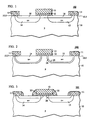
- an n-channel MOS transistor device structure 100 includes a portion 10 of a p-type silicon semiconductor body. Upon a top major surface 10.5 of this body 10 are located a relatively thick field oxide layer 11 and a thin gate oxide layer 12. Typically this gate oxide layer 12 has a thickness of about 12 nanometer or less for a channel length (gate oxide length) of about 0.8 micrometer or less. Upon the gate oxide layer 12 is located an n+ polycrystalline silicon gate electrode 13, as known in the art. Source and drain regions 14 and 15, respectively, are of n+ type conductivity, typically as formed by ion implantation of 80 keV arsenic followed by annealing, typically at about 900 degrees C for about 10 minutes. Metal or metal silicide source and drain electrodes (not shown) are typically attached to the respective surfaces of the source and drain regions, to complete the transistor device 100 and to supply it with electrical access to the rest of the circuit (not shown) integrated in the silicon body.
- the transistor device structure 100 is quite conventional.
- the device structure 100 further comprises a neutral impurity region in the form of a germanium doped region 16 formed prior to definition or formation of the gate electrode 13 but subsequent to the formation and patterning of the field oxide 11.
- the germanium region is formed, by example, by implantation with two doses of germanium ions, one having an energy of 25 keV and the other having an energy of 110 keV, using a standard source of germanium ions. Annealing is then performed at a temperature of about 950 degrees C, typically for approximately 30 to 60 minutes.
- this annealing of the germanium region which is performed advantageously for a longer time or at a higher temperature (or both) than the annealing of the arsenic at the source and drain, is performed prior to formation--as by the arsenic implantation--of the source and drain region. Because of the relatively low diffusivity of germanium in silicon, this annealing does not significantly change the depth of the germanium doped region 16.
- an MOS transistor device structure 200 has a similar structure to that of the previously described transistor device 100 except the germanium is implanted subsequent to the formation of the gate, and either prior or subsequent to the formation of the source and drain regions 14 and 15; and, in addition to the 25 keV and 110 keV doses of germanium used for the previously described structure 100, a dose of 160 keV (or higher) germanium is implanted into the body 10 in order to ensure that a portion of the germanium region 26 extends outside the metallurgical p-n junction 25 of the drain region 15 laterally into and substantially all the way across the width of the channel (at the surface 10.5 underneath the gate oxide layer 12), where it can suppress hot charge carrier formation.
- an annealing of the germanium region preferably is performed prior to source and drain implantation.
- an MOS transistor device structure 300 has a similar structure to that of the previously described device structure 200 except for the presence of a side-wall oxide (or other insulator) layer 32.
- the implantation of arsenic to form the source and drain regions is performed subsequent to side-wall oxide formation; whereas the implantation of the germanium to form the germanium doped region 36 is performed prior to side-wall oxide layer formation, in order to ensure that a portion of the germanium region 36 extends outside the drain region 15 laterally into (and across) the channel.
- Transistor devices of the kind shown in FIGS. 1,2, and 3 have been fabricated and successfully tested, and the implantations of germanium to concentration in the approximate range of 3x10¹⁷ to 1x10²⁰ (3E17 to 1E20) per cubic centimeter have resulted in significant improvements (reductions) in the rate of degradation of the transconductance. More specifically, to obtain the germanium concentration of 3E17 per cubic centimeter, a dose of 1E12 per square centimeter of 25 keV germanium ions plus a dose of 3E12 per square centimeter of 110 keV germanium ions (plus a dose of 3E12 per square centimeter of 160 keV germanium ions in the case of the structure 200) can be used.
- germanium concentration of 1E20 per cubic centimeter a dose of 3E14 per square centimeter of 25 keV germanium ions plus a dose of 1E15 per square centimeter of 110 keV germanium ions can be used. It should be noted that doses of germanium in an amount above about 3E19 per cubic centimeter produce amorphous silicon; doses below that amount produce damaged silicon. Higher germanium concentration than 1E20 per cubic centimeter may prove to be useful in conjunction with higher annealing temperatures. It should be noted, however, that experiments performed thus far on structures of the kind shown in FIG. 1 have indicated that the germanium concentration in this kind of structure (but not in structures like 200 and 300) should be limited to not more than 1E19 per cubic centimeter.
- the polysilicon gate can be a p+ polysilicon or a metal gate, instead of a n+ polysilicon gate.
- p-channel silicon MOS transistors similarly can benefit from neutral germanium regions in the neighborhood of the drain junction.
- both p-channel and n-channel transistor devices can be interconnected and integrated in the same silicon body, as known in the complementary MOS (CMOS) integrated circuit art, with either or both of these types of devices having the neutral germanium impurity regions described above, to reduce the rate of device degradation.
- CMOS complementary MOS
- MOS transistor devices of this invention can be interconnected and integrated with bipolar transistors in the same semiconductor body.
- a single annealing step can be used to repair simultaneously both the germanium and the arsenic damage at a temperature and for a time sufficient for repairing the damage due to the germanium implantation.
- the parameters of such a single annealing step must be carefully adjusted to ensure that in the device 200 the germanium region 26 extends beyond the metallurgical p-n junction 25 into the p-type silicon body 10 everywhere in a neighborhood of at least one-half the intersection of the metallurgical p-n junction 25 with the surface 10.5, such neighborhood thus extending laterally beyond the junction into the channel for a distance advantageously equal to at least approximately 0.01 micrometer.
- the neutral impurity region encompasses the regions of the devices where detrimental hot carriers are formed, particularly at or near (or both) an intersection of a p-n junction with a semiconductor surface.
Description
- This invention relates to semiconductor devices and more particularly to transistor device structures in integrated circuits and to methods for making such structures.
- It is known in the art that semiconductor devices, particularly both bipolar and MOS (metal oxide semiconductor) transistor devices, tend to degrade with use. That is, for example, the transconductances GM of these devices undesirably continue to decrease after continued operation in the circuits. More specifically, for a given MOS transistor, a higher drain-to-source voltage VDS causes a higher rate of undesirable reduction of GM and hence a lower lifetime of useful operation (operational lifetime) of the transistor.
- Each such device subject to this degradation is incorporated in a semiconductor body, typically silicon; and the device comprises a p-n junction, formed by the interface of two regions of the semiconductor body, one of the regions having a relatively high concentration of (conductivity-type determining) donor or acceptor impurities, the other having a relatively low concentration of acceptor or donor impurities, respectively--i.e., a p⁺n or an n⁺p junction, respectively. The p-n junction intersects the surface of the body at a location where the body is coated with an insulating layer. Degradation is believed to be caused by damage produced in the insulating layer by "hot" (fast-moving) charge carriers which are created in the region of relatively low impurity concentration, particularly in the neighborhood of the intersection of the p-n junction with the surface of the body. Accordingly, because of the higher electric fields which are ordinarily present in smaller sized devices and which cause a more severe hot charge carrier problem, smaller sized devices tend to have lower operational lifetimes.
- In U.S. Patent No. 4,704,547 issued to H. Kirsch on November 3, 1987, entitled "IGFET Gating Circuit Having Reduced Electric Field Degradation," it was taught that the degradation of MOS transistors due to hot carriers could be alleviated in complementary transistor logic gates by the technique of inserting an extra (protective) transistor between the p-channel and n-channel transistors. However, the technique of that patent requires the added transistor, which may be undesirable from the standpoints of speed performance and of consuming precious semiconductor surface area, particularly in complex logic circuits; and the technique may not be convenient to use in the context of circuits other than complementary transistor logic gates and the like.
- Another technique for reducing MOS transistor degradation is the lightly doped drain (LDD), in which the concentration of conductivity-type determining impurities is reduced in a neighborhood of the drain. However, in this technique unwanted added series resistance in the drain outside the transistor channel is unavoidable, whereby the switching speed of the transistor is undesirably reduced, especially when the added resistance is comparable to the resistance of the channel itself, as is the case where the channel length is approximately 0.5 micrometer or less.
- Yet another technique for coping with the hot carrier problem is a reduction in drain-source operating voltages. This technique, however, entails not only loss of speed but also a reduction in tolerable noise margins. Moreover, in case the channel length goes to approximately 0.5 micrometer or less, the reduction in drain-source operating voltages would present a serious obstacle to the use of Bipolar Complementary MOS (BiCMOS) circuits because of the higher minimum operating voltage requirements of the bipolar transistors in such circuits.
- It would therefore be desirable to have a technique for reducing the rate of degradation (increase the operational lifetime) of MOS transistors, which does not suffer from the aforementioned problems.
- EP-A-0419256, which forms part of the state of the art by virtue of Article 54(3)EPC, discloses a MOSFET doped with carbon in the channel region at the interface with the gate oxide to suppress hot electron trapping. The concentration is in the range 10¹⁶ - 10²⁰cm⁻³.
- Patent Abstracts of Japan, vol.11, no.31 (E-475) (2478) 29th January 1987 (JP-A-61-198681) discloses a MOS device with Ne, Ar, Kr or Xe implanted into the portions of the source and drain regions adjacent to the channel, to prevent hot electrons from being trapped in the gate oxide layer.
- US-A-4837173 discloses implantation of Ge ions near the location of the source and drain regions at a dose of 10¹⁵cm⁻².
- The aforementioned problems in the prior art techniques for increasing the operating lifetime (reducing the rate of degradation) of a semiconductor device, incorporated in a semiconductor body at a major surface thereof and having a p-n junction which intersects the major surface, are alleviated in a transistor as set out in claim 1.
- It is believed that this decrease in degradation is attributable--for example, in MOS transistors--to a prevention of the formation of hot charge carriers at or near the drain, or both, by virtue of scattering of the carriers by the germanium atoms. It is theorized that this scattering reduces the number of hot charge carriers that can penetrate to the insulating layer, where the hot carriers damage the insulating layer and degrade device performance. Because they are neutral, moreover, the added germanium atoms apparently do not significantly reduce the desirable mobility of charge carriers in the channel. However, it should be understood that the successful results obtained in this invention do not depend upon the correctness of any theory.
- Advantageously, in order to ensure p-n junctions that are shallow, any required relatively high temperature annealing of the neutral germanium region can be (but not necessarily) performed prior to implanting the conductivity-type determining impurity required to form the p-n junction (which thereafter generally requires a relatively low-temperature annealing).
-
- FIG. 1 is a cross-section diagram of an MOS transistor device in accordance with a specific embodiment of the invention;
- FIG. 2 is a cross-section diagram of an MOS transistor device in accordance with another specific embodiment of the invention; and
- FIG. 3 is a cross-section diagram of an MOS transistor device in accordance with yet another specific embodiment of the invention.
- Only for the sake of clarity, none of the drawings is to scale. Elements in different FIGURES which are substantially the same are denoted by the same reference numerals.
- As shown in FIG. 1 an n-channel MOS
transistor device structure 100 includes aportion 10 of a p-type silicon semiconductor body. Upon a top major surface 10.5 of thisbody 10 are located a relatively thickfield oxide layer 11 and a thingate oxide layer 12. Typically thisgate oxide layer 12 has a thickness of about 12 nanometer or less for a channel length (gate oxide length) of about 0.8 micrometer or less. Upon thegate oxide layer 12 is located an n⁺ polycrystallinesilicon gate electrode 13, as known in the art. Source anddrain regions transistor device 100 and to supply it with electrical access to the rest of the circuit (not shown) integrated in the silicon body. - As thus far described, the
transistor device structure 100 is quite conventional. In accordance with this embodiment (FIG. 1) of the invention, however, thedevice structure 100 further comprises a neutral impurity region in the form of a germanium dopedregion 16 formed prior to definition or formation of thegate electrode 13 but subsequent to the formation and patterning of thefield oxide 11. At that stage, the germanium region is formed, by example, by implantation with two doses of germanium ions, one having an energy of 25 keV and the other having an energy of 110 keV, using a standard source of germanium ions. Annealing is then performed at a temperature of about 950 degrees C, typically for approximately 30 to 60 minutes. Preferably, however, to ensure shallow source and drain junctions, this annealing of the germanium region, which is performed advantageously for a longer time or at a higher temperature (or both) than the annealing of the arsenic at the source and drain, is performed prior to formation--as by the arsenic implantation--of the source and drain region. Because of the relatively low diffusivity of germanium in silicon, this annealing does not significantly change the depth of the germanium dopedregion 16. - In another embodiment (FIG. 2) of the invention, an MOS
transistor device structure 200 has a similar structure to that of the previously describedtransistor device 100 except the germanium is implanted subsequent to the formation of the gate, and either prior or subsequent to the formation of the source anddrain regions structure 100, a dose of 160 keV (or higher) germanium is implanted into thebody 10 in order to ensure that a portion of thegermanium region 26 extends outside themetallurgical p-n junction 25 of thedrain region 15 laterally into and substantially all the way across the width of the channel (at the surface 10.5 underneath the gate oxide layer 12), where it can suppress hot charge carrier formation. Again, an annealing of the germanium region preferably is performed prior to source and drain implantation. - In yet another embodiment (FIG. 3) of the invention an MOS
transistor device structure 300 has a similar structure to that of the previously describeddevice structure 200 except for the presence of a side-wall oxide (or other insulator)layer 32. The implantation of arsenic to form the source and drain regions is performed subsequent to side-wall oxide formation; whereas the implantation of the germanium to form the germanium dopedregion 36 is performed prior to side-wall oxide layer formation, in order to ensure that a portion of thegermanium region 36 extends outside thedrain region 15 laterally into (and across) the channel. In view of the offset of thedrain region 15 relative to the germanium dopedregion 36 caused by the side-wall oxide formation, there is no need for a 160 keV germanium dose in addition to the 25 and 110 keV doses. Again, preferably an annealing of the germanium region is performed prior to the implantation of the source and drain regions. - Transistor devices of the kind shown in FIGS. 1,2, and 3 have been fabricated and successfully tested, and the implantations of germanium to concentration in the approximate range of 3x10¹⁷ to 1x10²⁰ (3E17 to 1E20) per cubic centimeter have resulted in significant improvements (reductions) in the rate of degradation of the transconductance. More specifically, to obtain the germanium concentration of 3E17 per cubic centimeter, a dose of 1E12 per square centimeter of 25 keV germanium ions plus a dose of 3E12 per square centimeter of 110 keV germanium ions (plus a dose of 3E12 per square centimeter of 160 keV germanium ions in the case of the structure 200) can be used. To obtain the germanium concentration of 1E20 per cubic centimeter, a dose of 3E14 per square centimeter of 25 keV germanium ions plus a dose of 1E15 per square centimeter of 110 keV germanium ions can be used. It should be noted that doses of germanium in an amount above about 3E19 per cubic centimeter produce amorphous silicon; doses below that amount produce damaged silicon. Higher germanium concentration than 1E20 per cubic centimeter may prove to be useful in conjunction with higher annealing temperatures. It should be noted, however, that experiments performed thus far on structures of the kind shown in FIG. 1 have indicated that the germanium concentration in this kind of structure (but not in structures like 200 and 300) should be limited to not more than 1E19 per cubic centimeter.
- Although the invention has been described in terms of specific embodiments, various modifications can be made without departing from the scope of the invention. For example, the polysilicon gate can be a p⁺ polysilicon or a metal gate, instead of a n⁺ polysilicon gate. Moreover, in addition to n-channel transistors, p-channel silicon MOS transistors similarly can benefit from neutral germanium regions in the neighborhood of the drain junction. Also both p-channel and n-channel transistor devices can be interconnected and integrated in the same silicon body, as known in the complementary MOS (CMOS) integrated circuit art, with either or both of these types of devices having the neutral germanium impurity regions described above, to reduce the rate of device degradation. In addition, MOS transistor devices of this invention can be interconnected and integrated with bipolar transistors in the same semiconductor body.
- Also, a single annealing step can be used to repair simultaneously both the germanium and the arsenic damage at a temperature and for a time sufficient for repairing the damage due to the germanium implantation. However, in the case of fabricating a device of the kind shown in FIG. 2, the parameters of such a single annealing step must be carefully adjusted to ensure that in the
device 200 thegermanium region 26 extends beyond the metallurgicalp-n junction 25 into the p-type silicon body 10 everywhere in a neighborhood of at least one-half the intersection of the metallurgicalp-n junction 25 with the surface 10.5, such neighborhood thus extending laterally beyond the junction into the channel for a distance advantageously equal to at least approximately 0.01 micrometer. - Instead of ion implantation, other methods can be used for obtaining a germanium region in silicon, such as epitaxially growing germanium-doped-silicon (silicon doped with germanium). Finally instead of silicon MOS transistors, other semiconductor devices, such as bipolar transistors, or diodes that suffer from hot carrier degradation can be used in conjunction with the neutral impurity regions of this invention. In the case of such bipolar transistors or diodes, advantageously the neutral impurity region encompasses the regions of the devices where detrimental hot carriers are formed, particularly at or near (or both) an intersection of a p-n junction with a semiconductor surface.
Claims (3)
- A MOS transistor formed in a device region of a first conductivity type in a silicon substrate, said transistor comprising a drain region (15) in a surface region of said device region forming a pn-junction with the device region and having a higher impurity concentration than the device region, a channel contiguous with the drain region, a portion (16, 26, 36) of the device region containing germanium atoms, the concentration of germanium atoms in the portion being at least 3×10¹⁷ atoms/cm³ and also being at least as high as the impurity concentration of the device region at the intersection of the pn-junction with the surface of the substrate, the portion being contiguous with at least one-half the intersection of said pn-junction with the surface (10.5) of the substrate, said portion extending laterally beyond the drain region into the channel for a distance of at least 0.01 »m.
- The transistor of claim 1 in which an insulating layer (11, 12) overlies the surface of the substrate where the pn-junction intersects it.
- An integrated circuit comprising the transistor recited in in claim 1 or 2.
Applications Claiming Priority (2)
| Application Number | Priority Date | Filing Date | Title |
|---|---|---|---|
| US41106189A | 1989-09-22 | 1989-09-22 | |
| US411061 | 1989-09-22 |
Publications (2)
| Publication Number | Publication Date |
|---|---|
| EP0419128A1 EP0419128A1 (en) | 1991-03-27 |
| EP0419128B1 true EP0419128B1 (en) | 1995-04-19 |
Family
ID=23627399
Family Applications (1)
| Application Number | Title | Priority Date | Filing Date |
|---|---|---|---|
| EP90310018A Expired - Lifetime EP0419128B1 (en) | 1989-09-22 | 1990-09-13 | Silicon MOSFET doped with germanium to increase lifetime of operation |
Country Status (5)
| Country | Link |
|---|---|
| US (1) | US5134447A (en) |
| EP (1) | EP0419128B1 (en) |
| JP (1) | JPH03119732A (en) |
| DE (1) | DE69018744T2 (en) |
| HK (1) | HK100396A (en) |
Families Citing this family (27)
| Publication number | Priority date | Publication date | Assignee | Title |
|---|---|---|---|---|
| US5245208A (en) * | 1991-04-22 | 1993-09-14 | Mitsubishi Denki Kabushiki Kaisha | Semiconductor device and manufacturing method thereof |
| US5137838A (en) * | 1991-06-05 | 1992-08-11 | National Semiconductor Corporation | Method of fabricating P-buried layers for PNP devices |
| JPH0521762A (en) * | 1991-07-10 | 1993-01-29 | Mitsubishi Electric Corp | Semiconductor device with fet and manufacture method |
| US5192712A (en) * | 1992-04-15 | 1993-03-09 | National Semiconductor Corporation | Control and moderation of aluminum in silicon using germanium and germanium with boron |
| DE4223914C2 (en) * | 1992-06-30 | 1996-01-25 | Fraunhofer Ges Forschung | Method for producing a vertical power component with a reduced minority carrier lifetime in its drift path |
| EP0622834A3 (en) * | 1993-04-30 | 1998-02-11 | International Business Machines Corporation | Method to prevent latch-up and improve breakdown voltage in SOI MOSFETS |
| JP3830541B2 (en) * | 1993-09-02 | 2006-10-04 | 株式会社ルネサステクノロジ | Semiconductor device and manufacturing method thereof |
| US5514902A (en) * | 1993-09-16 | 1996-05-07 | Mitsubishi Denki Kabushiki Kaisha | Semiconductor device having MOS transistor |
| JP3361922B2 (en) * | 1994-09-13 | 2003-01-07 | 株式会社東芝 | Semiconductor device |
| US6331458B1 (en) * | 1994-10-11 | 2001-12-18 | Advanced Micro Devices, Inc. | Active region implant methodology using indium to enhance short channel performance of a surface channel PMOS device |
| EP0717435A1 (en) * | 1994-12-01 | 1996-06-19 | AT&T Corp. | Process for controlling dopant diffusion in a semiconductor layer and semiconductor layer formed thereby |
| US5634001A (en) * | 1995-06-07 | 1997-05-27 | International Business Machines Corporation | Method to calculate hot-electron test voltage differential for assessing microprocessor reliability |
| US5650350A (en) * | 1995-08-11 | 1997-07-22 | Micron Technology, Inc. | Semiconductor processing method of forming a static random access memory cell and static random access memory cell |
| US5821147A (en) * | 1995-12-11 | 1998-10-13 | Lucent Technologies, Inc. | Integrated circuit fabrication |
| US5770485A (en) * | 1997-03-04 | 1998-06-23 | Advanced Micro Devices, Inc. | MOSFET device with an amorphized source and fabrication method thereof |
| US6225151B1 (en) | 1997-06-09 | 2001-05-01 | Advanced Micro Devices, Inc. | Nitrogen liner beneath transistor source/drain regions to retard dopant diffusion |
| EP0926739A1 (en) | 1997-12-24 | 1999-06-30 | Texas Instruments Incorporated | A structure of and method for forming a mis field effect transistor |
| US6030863A (en) * | 1998-09-11 | 2000-02-29 | Taiwan Semiconductor Manufacturing Company | Germanium and arsenic double implanted pre-amorphization process for salicide technology |
| US6124627A (en) * | 1998-12-03 | 2000-09-26 | Texas Instruments Incorporated | Lateral MOSFET having a barrier between the source/drain region and the channel region using a heterostructure raised source/drain region |
| DE10030381B4 (en) * | 2000-06-21 | 2005-04-14 | eupec Europäische Gesellschaft für Leistungshalbleiter mbH & Co. KG | Power semiconductor device comprising a body of semiconductor material with transition between mutually opposite conductivity types |
| US6777275B1 (en) * | 2000-11-15 | 2004-08-17 | Advanced Micro Devices, Inc. | Single anneal for dopant activation and silicide formation |
| US6638802B1 (en) * | 2002-06-20 | 2003-10-28 | Intel Corporation | Forming strained source drain junction field effect transistors |
| US20050104092A1 (en) * | 2003-11-19 | 2005-05-19 | International Business Machiness Corportion | Method of reducing dislocation-induced leakage in a strained-layer field-effect transistor |
| DE102005042827A1 (en) | 2005-09-09 | 2007-03-22 | Atmel Germany Gmbh | High-voltage FET with source drain gate and channel has doped drift region having potential barrier spaced from the body region |
| WO2007126807A1 (en) * | 2006-04-28 | 2007-11-08 | Advanced Micro Devices, Inc. | An soi transistor having a reduced body potential and a method of forming the same |
| DE102006019935B4 (en) | 2006-04-28 | 2011-01-13 | Advanced Micro Devices, Inc., Sunnyvale | Reduced body potential SOI transistor and method of manufacture |
| US8101489B2 (en) * | 2008-01-28 | 2012-01-24 | Taiwan Semiconductor Manufacturing Company, Ltd. | Approach to reduce the contact resistance |
Citations (1)
| Publication number | Priority date | Publication date | Assignee | Title |
|---|---|---|---|---|
| EP0419256A1 (en) * | 1989-09-21 | 1991-03-27 | Hewlett-Packard Company | Carbon doping MOSFET substrate to suppress hot electron trapping |
Family Cites Families (9)
| Publication number | Priority date | Publication date | Assignee | Title |
|---|---|---|---|---|
| US4636822A (en) * | 1984-08-27 | 1987-01-13 | International Business Machines Corporation | GaAs short channel lightly doped drain MESFET structure and fabrication |
| US4603471A (en) * | 1984-09-06 | 1986-08-05 | Fairchild Semiconductor Corporation | Method for making a CMOS circuit having a reduced tendency to latch by controlling the band-gap of source and drain regions |
| US4680603A (en) * | 1985-04-12 | 1987-07-14 | General Electric Company | Graded extended drain concept for reduced hot electron effect |
| US4613882A (en) * | 1985-04-12 | 1986-09-23 | General Electric Company | Hybrid extended drain concept for reduced hot electron effect |
| CA1216962A (en) * | 1985-06-28 | 1987-01-20 | Hussein M. Naguib | Mos device processing |
| US4843023A (en) * | 1985-09-25 | 1989-06-27 | Hewlett-Packard Company | Process for forming lightly-doped-drain (LDD) without extra masking steps |
| US4837173A (en) * | 1987-07-13 | 1989-06-06 | Motorola, Inc. | N-channel MOS transistors having source/drain regions with germanium |
| JPH01112772A (en) * | 1987-10-27 | 1989-05-01 | Fujitsu Ltd | Mis-type semiconductor device |
| US4835112A (en) * | 1988-03-08 | 1989-05-30 | Motorola, Inc. | CMOS salicide process using germanium implantation |
-
1990
- 1990-08-27 US US07/574,564 patent/US5134447A/en not_active Expired - Lifetime
- 1990-09-13 EP EP90310018A patent/EP0419128B1/en not_active Expired - Lifetime
- 1990-09-13 DE DE69018744T patent/DE69018744T2/en not_active Expired - Fee Related
- 1990-09-21 JP JP2250429A patent/JPH03119732A/en active Pending
-
1996
- 1996-06-06 HK HK100396A patent/HK100396A/en unknown
Patent Citations (1)
| Publication number | Priority date | Publication date | Assignee | Title |
|---|---|---|---|---|
| EP0419256A1 (en) * | 1989-09-21 | 1991-03-27 | Hewlett-Packard Company | Carbon doping MOSFET substrate to suppress hot electron trapping |
Also Published As
| Publication number | Publication date |
|---|---|
| DE69018744D1 (en) | 1995-05-24 |
| EP0419128A1 (en) | 1991-03-27 |
| HK100396A (en) | 1996-06-14 |
| US5134447A (en) | 1992-07-28 |
| DE69018744T2 (en) | 1996-01-11 |
| JPH03119732A (en) | 1991-05-22 |
Similar Documents
| Publication | Publication Date | Title |
|---|---|---|
| EP0419128B1 (en) | Silicon MOSFET doped with germanium to increase lifetime of operation | |
| US5510279A (en) | Method of fabricating an asymmetric lightly doped drain transistor device | |
| JP4708563B2 (en) | Method for reducing the effective channel length of a lightly doped drain transistor and method for forming a transistor | |
| US5548143A (en) | Metal oxide semiconductor transistor and a method for manufacturing the same | |
| US6531739B2 (en) | Radiation-hardened silicon-on-insulator CMOS device, and method of making the same | |
| JP3164076B2 (en) | Method for manufacturing semiconductor device | |
| US5041885A (en) | Surface field effect transistor with depressed source and/or drain areas for ULSI integrated devices | |
| KR20000069811A (en) | Well boosting threshold voltage rollup | |
| US5536959A (en) | Self-aligned charge screen (SACS) field effect transistors and methods | |
| JPH08330587A (en) | Method for manufacturing integrated circuit, and method for replenishing both diffusion and segregation of boron from channel and field regions to source and drain regions adjacent thereto | |
| EP0718892A2 (en) | Semiconductor device including insulated gate bipolar transistor and method of fabricating the same | |
| US6297098B1 (en) | Tilt-angle ion implant to improve junction breakdown in flash memory application | |
| US5021851A (en) | NMOS source/drain doping with both P and As | |
| US4839301A (en) | Blanket CMOS channel stop implant employing a combination of n-channel and p-channel punch-through implants | |
| US4851360A (en) | NMOS source/drain doping with both P and As | |
| US20040041170A1 (en) | Low dose super deep source/drain implant | |
| US7524710B2 (en) | Radiation-hardened silicon-on-insulator CMOS device, and method of making the same | |
| KR19980050121A (en) | Transistor and manufacturing method | |
| US5963809A (en) | Asymmetrical MOSFET with gate pattern after source/drain formation | |
| US6476430B1 (en) | Integrated circuit | |
| JPS5893279A (en) | Manufacture of semiconductor device | |
| US5399514A (en) | Method for manufacturing improved lightly doped diffusion (LDD) semiconductor device | |
| US5422510A (en) | MOS transistor with non-uniform channel dopant profile | |
| JP3144385B2 (en) | Semiconductor device and manufacturing method thereof | |
| JPH04127537A (en) | Manufacture of mosfet |
Legal Events
| Date | Code | Title | Description |
|---|---|---|---|
| PUAI | Public reference made under article 153(3) epc to a published international application that has entered the european phase |
Free format text: ORIGINAL CODE: 0009012 |
|
| AK | Designated contracting states |
Kind code of ref document: A1 Designated state(s): DE FR GB |
|
| 17P | Request for examination filed |
Effective date: 19910918 |
|
| 17Q | First examination report despatched |
Effective date: 19930730 |
|
| RAP3 | Party data changed (applicant data changed or rights of an application transferred) |
Owner name: AT&T CORP. |
|
| GRAA | (expected) grant |
Free format text: ORIGINAL CODE: 0009210 |
|
| AK | Designated contracting states |
Kind code of ref document: B1 Designated state(s): DE FR GB |
|
| ET | Fr: translation filed | ||
| REF | Corresponds to: |
Ref document number: 69018744 Country of ref document: DE Date of ref document: 19950524 |
|
| PGFP | Annual fee paid to national office [announced via postgrant information from national office to epo] |
Ref country code: GB Payment date: 19950717 Year of fee payment: 6 |
|
| PGFP | Annual fee paid to national office [announced via postgrant information from national office to epo] |
Ref country code: DE Payment date: 19950823 Year of fee payment: 6 |
|
| PGFP | Annual fee paid to national office [announced via postgrant information from national office to epo] |
Ref country code: FR Payment date: 19950824 Year of fee payment: 6 |
|
| PLBE | No opposition filed within time limit |
Free format text: ORIGINAL CODE: 0009261 |
|
| STAA | Information on the status of an ep patent application or granted ep patent |
Free format text: STATUS: NO OPPOSITION FILED WITHIN TIME LIMIT |
|
| 26N | No opposition filed | ||
| PG25 | Lapsed in a contracting state [announced via postgrant information from national office to epo] |
Ref country code: GB Effective date: 19960913 |
|
| PG25 | Lapsed in a contracting state [announced via postgrant information from national office to epo] |
Ref country code: FR Effective date: 19960930 |
|
| GBPC | Gb: european patent ceased through non-payment of renewal fee |
Effective date: 19960913 |
|
| PG25 | Lapsed in a contracting state [announced via postgrant information from national office to epo] |
Ref country code: DE Effective date: 19970603 |
|
| REG | Reference to a national code |
Ref country code: FR Ref legal event code: ST |
|
| REG | Reference to a national code |
Ref country code: FR Ref legal event code: ST |