EP1265216A2 - Operationelle Verstärkerschaltung, Treiberschaltung und -Verfahren - Google Patents
Operationelle Verstärkerschaltung, Treiberschaltung und -Verfahren Download PDFInfo
- Publication number
- EP1265216A2 EP1265216A2 EP02012195A EP02012195A EP1265216A2 EP 1265216 A2 EP1265216 A2 EP 1265216A2 EP 02012195 A EP02012195 A EP 02012195A EP 02012195 A EP02012195 A EP 02012195A EP 1265216 A2 EP1265216 A2 EP 1265216A2
- Authority
- EP
- European Patent Office
- Prior art keywords
- voltage level
- operational amplifier
- data line
- counter electrode
- power source
- Prior art date
- Legal status (The legal status is an assumption and is not a legal conclusion. Google has not performed a legal analysis and makes no representation as to the accuracy of the status listed.)
- Granted
Links
Images


Classifications
-
- G—PHYSICS
- G09—EDUCATION; CRYPTOGRAPHY; DISPLAY; ADVERTISING; SEALS
- G09G—ARRANGEMENTS OR CIRCUITS FOR CONTROL OF INDICATING DEVICES USING STATIC MEANS TO PRESENT VARIABLE INFORMATION
- G09G3/00—Control arrangements or circuits, of interest only in connection with visual indicators other than cathode-ray tubes
- G09G3/20—Control arrangements or circuits, of interest only in connection with visual indicators other than cathode-ray tubes for presentation of an assembly of a number of characters, e.g. a page, by composing the assembly by combination of individual elements arranged in a matrix no fixed position being assigned to or needed to be assigned to the individual characters or partial characters
- G09G3/34—Control arrangements or circuits, of interest only in connection with visual indicators other than cathode-ray tubes for presentation of an assembly of a number of characters, e.g. a page, by composing the assembly by combination of individual elements arranged in a matrix no fixed position being assigned to or needed to be assigned to the individual characters or partial characters by control of light from an independent source
- G09G3/36—Control arrangements or circuits, of interest only in connection with visual indicators other than cathode-ray tubes for presentation of an assembly of a number of characters, e.g. a page, by composing the assembly by combination of individual elements arranged in a matrix no fixed position being assigned to or needed to be assigned to the individual characters or partial characters by control of light from an independent source using liquid crystals
-
- G—PHYSICS
- G09—EDUCATION; CRYPTOGRAPHY; DISPLAY; ADVERTISING; SEALS
- G09G—ARRANGEMENTS OR CIRCUITS FOR CONTROL OF INDICATING DEVICES USING STATIC MEANS TO PRESENT VARIABLE INFORMATION
- G09G3/00—Control arrangements or circuits, of interest only in connection with visual indicators other than cathode-ray tubes
- G09G3/20—Control arrangements or circuits, of interest only in connection with visual indicators other than cathode-ray tubes for presentation of an assembly of a number of characters, e.g. a page, by composing the assembly by combination of individual elements arranged in a matrix no fixed position being assigned to or needed to be assigned to the individual characters or partial characters
- G09G3/2007—Display of intermediate tones
- G09G3/2011—Display of intermediate tones by amplitude modulation
-
- G—PHYSICS
- G09—EDUCATION; CRYPTOGRAPHY; DISPLAY; ADVERTISING; SEALS
- G09G—ARRANGEMENTS OR CIRCUITS FOR CONTROL OF INDICATING DEVICES USING STATIC MEANS TO PRESENT VARIABLE INFORMATION
- G09G3/00—Control arrangements or circuits, of interest only in connection with visual indicators other than cathode-ray tubes
- G09G3/20—Control arrangements or circuits, of interest only in connection with visual indicators other than cathode-ray tubes for presentation of an assembly of a number of characters, e.g. a page, by composing the assembly by combination of individual elements arranged in a matrix no fixed position being assigned to or needed to be assigned to the individual characters or partial characters
- G09G3/34—Control arrangements or circuits, of interest only in connection with visual indicators other than cathode-ray tubes for presentation of an assembly of a number of characters, e.g. a page, by composing the assembly by combination of individual elements arranged in a matrix no fixed position being assigned to or needed to be assigned to the individual characters or partial characters by control of light from an independent source
- G09G3/36—Control arrangements or circuits, of interest only in connection with visual indicators other than cathode-ray tubes for presentation of an assembly of a number of characters, e.g. a page, by composing the assembly by combination of individual elements arranged in a matrix no fixed position being assigned to or needed to be assigned to the individual characters or partial characters by control of light from an independent source using liquid crystals
- G09G3/3611—Control of matrices with row and column drivers
- G09G3/3685—Details of drivers for data electrodes
- G09G3/3688—Details of drivers for data electrodes suitable for active matrices only
-
- H—ELECTRICITY
- H03—ELECTRONIC CIRCUITRY
- H03K—PULSE TECHNIQUE
- H03K5/00—Manipulating of pulses not covered by one of the other main groups of this subclass
- H03K5/01—Shaping pulses
- H03K5/08—Shaping pulses by limiting; by thresholding; by slicing, i.e. combined limiting and thresholding
- H03K5/082—Shaping pulses by limiting; by thresholding; by slicing, i.e. combined limiting and thresholding with an adaptive threshold
- H03K5/086—Shaping pulses by limiting; by thresholding; by slicing, i.e. combined limiting and thresholding with an adaptive threshold generated by feedback
-
- H—ELECTRICITY
- H03—ELECTRONIC CIRCUITRY
- H03K—PULSE TECHNIQUE
- H03K5/00—Manipulating of pulses not covered by one of the other main groups of this subclass
- H03K5/22—Circuits having more than one input and one output for comparing pulses or pulse trains with each other according to input signal characteristics, e.g. slope, integral
- H03K5/24—Circuits having more than one input and one output for comparing pulses or pulse trains with each other according to input signal characteristics, e.g. slope, integral the characteristic being amplitude
- H03K5/2472—Circuits having more than one input and one output for comparing pulses or pulse trains with each other according to input signal characteristics, e.g. slope, integral the characteristic being amplitude using field effect transistors
- H03K5/2481—Circuits having more than one input and one output for comparing pulses or pulse trains with each other according to input signal characteristics, e.g. slope, integral the characteristic being amplitude using field effect transistors with at least one differential stage
-
- G—PHYSICS
- G09—EDUCATION; CRYPTOGRAPHY; DISPLAY; ADVERTISING; SEALS
- G09G—ARRANGEMENTS OR CIRCUITS FOR CONTROL OF INDICATING DEVICES USING STATIC MEANS TO PRESENT VARIABLE INFORMATION
- G09G2330/00—Aspects of power supply; Aspects of display protection and defect management
- G09G2330/02—Details of power systems and of start or stop of display operation
- G09G2330/021—Power management, e.g. power saving
-
- G—PHYSICS
- G09—EDUCATION; CRYPTOGRAPHY; DISPLAY; ADVERTISING; SEALS
- G09G—ARRANGEMENTS OR CIRCUITS FOR CONTROL OF INDICATING DEVICES USING STATIC MEANS TO PRESENT VARIABLE INFORMATION
- G09G3/00—Control arrangements or circuits, of interest only in connection with visual indicators other than cathode-ray tubes
- G09G3/20—Control arrangements or circuits, of interest only in connection with visual indicators other than cathode-ray tubes for presentation of an assembly of a number of characters, e.g. a page, by composing the assembly by combination of individual elements arranged in a matrix no fixed position being assigned to or needed to be assigned to the individual characters or partial characters
- G09G3/34—Control arrangements or circuits, of interest only in connection with visual indicators other than cathode-ray tubes for presentation of an assembly of a number of characters, e.g. a page, by composing the assembly by combination of individual elements arranged in a matrix no fixed position being assigned to or needed to be assigned to the individual characters or partial characters by control of light from an independent source
- G09G3/36—Control arrangements or circuits, of interest only in connection with visual indicators other than cathode-ray tubes for presentation of an assembly of a number of characters, e.g. a page, by composing the assembly by combination of individual elements arranged in a matrix no fixed position being assigned to or needed to be assigned to the individual characters or partial characters by control of light from an independent source using liquid crystals
- G09G3/3611—Control of matrices with row and column drivers
- G09G3/3614—Control of polarity reversal in general
-
- G—PHYSICS
- G09—EDUCATION; CRYPTOGRAPHY; DISPLAY; ADVERTISING; SEALS
- G09G—ARRANGEMENTS OR CIRCUITS FOR CONTROL OF INDICATING DEVICES USING STATIC MEANS TO PRESENT VARIABLE INFORMATION
- G09G3/00—Control arrangements or circuits, of interest only in connection with visual indicators other than cathode-ray tubes
- G09G3/20—Control arrangements or circuits, of interest only in connection with visual indicators other than cathode-ray tubes for presentation of an assembly of a number of characters, e.g. a page, by composing the assembly by combination of individual elements arranged in a matrix no fixed position being assigned to or needed to be assigned to the individual characters or partial characters
- G09G3/34—Control arrangements or circuits, of interest only in connection with visual indicators other than cathode-ray tubes for presentation of an assembly of a number of characters, e.g. a page, by composing the assembly by combination of individual elements arranged in a matrix no fixed position being assigned to or needed to be assigned to the individual characters or partial characters by control of light from an independent source
- G09G3/36—Control arrangements or circuits, of interest only in connection with visual indicators other than cathode-ray tubes for presentation of an assembly of a number of characters, e.g. a page, by composing the assembly by combination of individual elements arranged in a matrix no fixed position being assigned to or needed to be assigned to the individual characters or partial characters by control of light from an independent source using liquid crystals
- G09G3/3611—Control of matrices with row and column drivers
- G09G3/3648—Control of matrices with row and column drivers using an active matrix
- G09G3/3655—Details of drivers for counter electrodes, e.g. common electrodes for pixel capacitors or supplementary storage capacitors
Definitions
- the present invention relates to an operational amplifier circuit, a driving circuit and a driving method.
- liquid crystal panel electro-optical device
- TFT thin film transistor
- the passive matrix type is advantageous compared to the active matrix type in that the lowering of power consumption can be easily obtained, the passive matrix type has a disadvantage that the multi-colorization and the moving picture display are difficult.
- a technique for lowering the power consumption in the passive matrix type there has been known a conventional technique disclosed in Japanese Laid-open Patent Publication 7-98577, for example.
- the active matrix type has an advantage that this type is suitable for the multi-colorization and the moving picture display, the active matrix type has a disadvantage that the lowering of the power consumption is difficult.
- the active matrix type liquid crystal panel is now popularly used.
- the present invention has been made in view of the above-mentioned technical problems, and according to the present invention, there are provided an operational amplifier circuit which can realize the reduction of power consumption of an electro-optical device using a simple circuit configuration and a driving circuit and a driving method using such an operational amplifier circuit.
- One aspect of the present invention provides an operational amplifier circuit which drives each of data lines of an electro-optical device having scan lines, data lines and pixel electrodes which are specified by the scan lines and the data lines, wherein an output of the operational amplifier circuit is set to a high impedance state in a given period including a transition between a first period in which a voltage level of a counter electrode becomes a first voltage level and a second period in which the voltage level of the counter electrode becomes a second voltage level, the counter electrode facing a pixel electrode with an electro-optical material interposed therebetween.
- the output of the operational amplifier circuit is set to the high impedance state (non-driving state).
- the output of the operational amplifier circuit is set to the high impedance state (non-driving state).
- the operational amplifier circuit may comprise:
- the operational amplifier circuit can drive the data line using the optimum operational amplifier corresponding to the change (inversion of polarity) of the voltage level of the counter electrode, and the lowering of the power consumption can be realized.
- the first operational amplifier may comprise:
- the data line can be driven by the first driving transistor of the first conductivity type during the first period and can be driven by the second driving transistor of the second conductivity type during the second period. Accordingly, it is possible to drive the data line with the proper driving transistor so that the lowering of power consumption of the operational amplifier circuit can be realized.
- a voltage level of a data line connected to an output of the operational amplifier circuit may be changed to a second power source side by setting an output of the operational amplifier circuit to the high impedance state and by using a capacitive coupling of a parasitic capacitance between the counter electrode and the data line, in a given period in which a voltage level of the counter electrode changes from a second voltage level of a first power source side to a first voltage level of a second power source side, and the voltage level of the data line connected to an output of the operational amplifier circuit may be changed to a first power source side by setting an output of the operational amplifier circuit to the high impedance state and by using the capacitive coupling of the parasitic capacitance between the counter electrode and the data line, in a given period in which a voltage level of the counter electrode changes from a first voltage level of a second power source side to a second voltage level of a first power source side.
- the operational amplifier circuit may include:
- the first or the second operational amplifier it is possible to use an operational amplifier having a high driving ability for only one of the first and the second power source sides so that an operational amplifier which exhibits a small power consumption can be used. Accordingly, the power consumption of the operational amplifier can be lowered.
- the operational amplifier circuit may include a clamp circuit which clamps an output of the operational amplifier circuit in a voltage range which is equal to or wider than a voltage range between first and second power sources of the operational amplifier circuits.
- a power source of the clamp circuit may be set to third and fourth power sources which have voltage ranges narrower than voltage ranges of the first and second power sources of the operational amplifier circuit.
- Another aspect of the present invention provides a driving circuit which drives an electro-optical device having scan lines, data lines and pixel electrodes which are specified by the scan lines and the data lines, the driving circuit comprising;
- a further aspect provides a method of driving an electro-optical device having scan lines, data lines and pixel electrodes which are specified by the scan lines and the data lines, the method comprising:
- the driving method may further comprise:
- the driving method may comprise:
- the driving method may comprise:
- Fig. 1 is a block diagram showing an example of a liquid crystal device to which an operational amplifier circuit of this embodiment is applied.
- the liquid crystal device 10 (display device in a broad sense) includes a display panel 12 (LCD (Liquid Crystal Display) panel in a narrow sense) , a data line driving circuit 20 (a source driver in a narrow sense), a scan line driving circuit 30 (gate driver in a narrow sense), a controller 40 and a power source circuit 42.
- the liquid crystal device 10 is not always required to include all of these circuit blocks and some circuit blocks may be omitted.
- the display panel 12 (electro-optical device in a broad sense) includes a plurality of scan lines (gate lines in a narrow sense), a plurality of data lines (source lines in a narrow sense) and pixel electrodes which are specified by the scan lines and the data lines.
- TFTs thin film transistors
- switching elements in a broad sense are connected to the data lines and the pixel electrodes are connected to the TFTs thus constituting an active matrix type liquid crystal device.
- the display panel 12 is formed as an active matrix substrate (glass substrate, for example).
- a plurality of scan lines G 1 to G M (M being a natural number of 2 or more) which are arranged in parallel in the Y direction in Fig. 1 and are respectively extended in the X direction in Fig. 1
- a plurality of data lines S 1 to S N (N being a natural number of 2 or more) which are arranged in parallel in the X direction in Fig. 1 and are respectively extended in the Y direction in Fig. 1 are arranged.
- a TFT KL switching element in a broad sense
- a gate electrode of the TFT KL is connected to the scan line G K , a source electrode of the TFT KL is connected to the data line S L , and a drain electrode of the TFT KL is connected to the pixel electrode PE KL .
- pixel electrode PE KL and a counter electrode VCOM common electrode which faces the pixel electrode PE KL with a liquid crystal element (electro-optical material in a broad sense) interposed therebetween.
- liquid crystal capacitance CL KL (liquid crystal element) and auxiliary capacitance CS KL are generated. Further, liquid crystal is filled between the active matrix substrate on which the TFT KL , pixel electrodes PE KL and the like are formed and a counter substrate on which the counter electrode VCOM is formed. The transmittance of the liquid crystal element is changed in response to a voltage applied between the pixel electrode PE KL and the counter electrode VCOM.
- the voltage levels (first and second voltage levels) applied to the counter electrode VCOM are generated by the power source circuit 42. Further, without forming the counter electrode VCOM in a matted manner on the counter substrate, it is possible to form counter electrodes VCOM in a strip shape such that they correspond to respective scan lines.
- the data line driving circuit 20 drives the data lines S 1 to S N of the display panel 12 based on the image data.
- the scan line driving circuit 30 sequentially performs the scanning driving of the scan lines G 1 to G M of the display panel 12.
- the controller 40 controls the data line driving circuit 20, the scan line driving circuit 30 and the power source circuit 42 in accordance with a content set by a host computer such as a central processing unit (hereinafter referred to as "CPU") not shown in the drawing. More specifically, the controller 40 performs the setting of operational modes and supplies vertical synchronous signals and horizontal synchronous signals which are generated in the inside of the controller 40 to the data line driving circuit 20 and the scan line driving circuit 30, while the controller 40 performs the control of polarity inversion timing of voltage level of the counter electrode VCOM.
- CPU central processing unit
- the power source circuit 42 generates various types of voltage levels (gray scale voltages) and the voltage level of the counter electrode VCOM necessary for driving the display panel 12 based on reference voltages supplied from the outside.
- the liquid crystal device 10 having such a configuration, under the control of the controller 40, based on the image data supplied from the outside, the data line driving circuit 20, the scan line driving circuit 30 and the power source circuit 42 drive the display panel 12 in a cooperative manner.
- the liquid crystal device 10 is configured to incorporate the controller 40 therein, the controller 40 maybe provided outside the liquid crystal device 10. Alternately, a host computer may be incorporated into the liquid crystal device 10 together with the controller 40. Further, a portion of or all of the data line driving circuit 20, the scan line driving circuit 30, the controller 40 and the power source circuit 42 may be formed on the display panel 12.
- Fig. 2 shows an example of the configuration of the data line driving circuit 20 shown in Fig. 1.
- the data line driving circuit 20 includes a shift register 22, line latches 24, 26, a DAC 28 (digital/analogue conversion circuit, data voltage generation circuit in a broad sense), and an output buffer 29 (operational amplifier circuits).
- the shift register 22 includes a plurality of flip-flops which are provided corresponding to respective data lines and are sequentially connected with each other.
- the shift register 22 holds enable input/output signals in synchronism with clock signals CLK and sequentially shifts the enable input/output signals EIO to neighboring flip-flops in synchronism with the clock signals CLK.
- the image data (DIO) is inputted to the line latch 24 per a unit of 18 bits (6 bits (gray scale data) ⁇ 3 (respective colors R, G, B)) from the controller 40, for example.
- the line latch 24 latches the image data (DIO) in synchronism with the enable input/output signals EIO which are sequentially shifted by respective flip-flops of the shift register 22.
- the line latch 26 latches the image data for 1 horizontal scanning unit which is latched by the line latch 24 in synchronism with horizontal synchronous signals LP supplied from the controller 40.
- the DAC 28 generates analogue data voltages to be supplied to respective data lines. More specifically, the DAC 28, based on digital image data from the line latch 26, selects any one of gray scale voltages from the power source circuit 42 shown in Fig. 1 and outputs the analogue data voltages corresponding to the digital image data.
- the output buffer 29 outputs the data voltages from the DAC 28 to the data lines after buffering them and drives the data lines. More specifically, the output buffer 29 includes operational amplifier circuits OPC in voltage follower connection provided for respective data lines and these operational amplifier circuits OPC output the data voltages from the DAC 28 to respective data lines after performing the impedance conversion.
- the data line driving circuit is configured such that the data line driving circuit 20 is configured such that the digital image data is subjected to the digital/analogue conversion and the analogue data is outputted to the data lines through the output buffer 29.
- the analogue video signals may be subjected to a sample holding and may be outputted to the data lines through the output buffer 29.
- Fig. 3 shows an example of the configuration of the scan line driving circuit 30 shown in Fig. 1.
- the scan line driving circuit 30 includes a shift register 32, a level shifter 34 and an output buffer 36.
- the shift register 32 includes a plurality of flip-flops which are provided corresponding to respective scan lines and are sequentially connected to each other.
- the shift register 32 when enable input/output signals EIO are held by the flip-flops in synchronism with clock signals CLK, sequentially shifts the enable input/output signals EIO to neighboring flip-flops in synchronism with the clock signals CLK.
- the inputted enable input/output signals EIO are vertical synchronous signals which are supplied from the controller 40.
- the level shifter 34 shifts the voltage levels outputted from the shift register 32 to the voltage levels corresponding to the capacities of the liquid crystal element of the display panel 12 and the TFTs.
- the high voltage level of 20V to 50V, for example, is necessary as the voltage level and hence, the high dielectric strength process different from that of the other logic circuit parts is used.
- the output buffer 36 outputs the scanning voltage which is shifted by the level shifter 34 after buffering the scanning voltage and drives the scan lines.
- the liquid crystal element has a property that when the direct current voltage is applied to the liquid crystal element for a long time, the liquid crystal element is deteriorated.
- a driving method which inverts the polarity of the voltage applied to the liquid crystal element every given period become necessary.
- a frame inversion driving there have been known a scanning (gate) line inversion driving, a data (source) line inversion driving method, a dot inversion driving and the like.
- the frame inversion driving method exhibits the lowering of power consumption
- the method has a disadvantage that the image quality is not so good.
- the data line inversion driving and the dot inversion driving exhibit the good image quality, these methods have a disadvantage that the high voltage is necessary for driving the display panel.
- this embodiment adopts the scan line inversion driving shown in Fig. 4.
- the voltage applied to the liquid crystal element has the polarity thereof inverted every scanning period (every scan line).
- the voltage of positive polarity is applied to the liquid crystal element during the first scanning period (scan line)
- the voltage of negative polarity is applied to the liquid crystal element during the second scanning period
- the voltage of positive polarity is applied to the liquid crystal element during the third scanning period.
- the voltage of negative polarity is applied to the liquid crystal element during the first scanning period
- the voltage of positive polarity is applied to the liquid crystal element during the second scanning period
- the voltage of negative polarity is applied to the liquid crystal element during the third scanning period.
- the voltage level of the counter electrode VCOM has the polarity thereof inverted every scanning period.
- the voltage level of the counter electrode VCOM becomes VC1 (first voltage level) during the period T1 of positive polarity (first period) and becomes VC2 (second voltage level) during the period T2 of negative polarity(second period).
- the period T1 of positive polarity is a period in which the voltage level of the data line S (pixel electrode) becomes higher than the voltage level of the counter electrode VCOM. During this period T1, the voltage of positive polarity is applied to the liquid crystal element.
- the period T2 of negative polarity is a period in which the voltage level of the data line S (pixel electrode) becomes lower than the voltage level of the counter electrode VCOM. During this period T2, the voltage of negative polarity is applied to the liquid crystal element.
- VC2 is the voltage level which is obtained by performing the inversion of polarity of VC1 with respect to a given voltage level.
- the voltage necessary for driving the display panel can be lowered. Accordingly, the dielectric strength of the driving circuit can be lowered leading to the simplifying of the manufacturing process and the reduction of the manufacturing cost.
- the voltage level of the data line S is changed to the low potential side as indicated by A1 in Fig. 5.
- the gray scale of the data line S during the period T1 is 0 and the gray scale of the data line S during the period T2 is also 0, the voltage level of the data line S is changed to the high potential side.
- an operational amplifier circuit including the output buffer 29 shown in Fig. 2 for driving the data line
- an AB class (push-pull method) operational amplifier circuit shown in Fig. 6 has been used.
- This AB class operational amplifier circuit includes a differential section 300 and an output section 310 which has a P-type (first conductivity type in a broad sense) driving transistor PT53 and an N-type (second conductivity type in a broad sense) driving transistor NT55.
- the differential section 300 includes P-type transistors PT51 and PT52 which have gate electrodes thereof connected to an output DQ of the differential section 300 in common, N-type transistors NT51 and NT52 which have gate electrodes thereof connected to inputs I and XI of the differential section 300, and a current source IS51.
- the output section 310 includes an inversion circuit which is constituted of an N-type transistor NT53 which has a gate electrode thereof connected to an output XDQ (inversion output) of the differential section 300 and a current source IS52. Further, the output section 310 includes the P-type driving transistor PT53 which has a gate electrode thereof connected to the output XDQ of the differential section 300, the N-type driving transistor NT55 which has a gate electrode thereof connected to an output BQ of the inversion circuit, an N-type transistor NT54 which has a gate electrode thereof connected to a VSS, and capacitance CC for phase compensation.
- an output Q of the output section 310 is connected to the input XI (inversion input) of the differential section 300 thus establishing a voltage follower connection.
- the current sources IS51 and IS52 are constituted of N-type transistors which have gate electrodes thereof connected to the reference voltage (constant voltage) , for example.
- the output section 310 includes both of the P-type driving transistor PT53 and the N-type driving transistor NT55. Accordingly, in the case of A1 and A4 in Fig. 5, the N-type driving transistor NT55 is operated so that the voltage level of the data line S can be rapidly lowered to the low potential side. On the other hand, in the case of A2 and A3 in Fig. 5, the P-type driving transistor PT53 is operated so that the voltage level of the data line S can be rapidly elevated to the high potential side. Accordingly, in the liquid crystal device which performs the scan line inversion driving while inverting the polarity of the counter electrode VCOM, in most cases, the AB class operational amplifier circuit shown in Fig. 6 has been used as an operational amplifier circuit which an output buffer of a data line driving circuit includes.
- the AB class operational amplifier circuit shown in Fig. 6 includes three paths in which an electric current flows, that is, the paths for electric currents I51, I52, I53 and hence, the electric current which is consumed uselessly is increased thus giving rise to a problem that the power consumption is increased.
- a circuit having a configuration which uses four or more current paths is used in many cases.
- the power consumption is further increased.
- the electric currents I51, I52 and I53 are reduced in amount to lower the power consumption, this brings about the lowering of response speed and the deterioration of frequency characteristics.
- this embodiment adopts a method which will be described hereinafter.
- the operational amplifiers for driving the data line are changed over corresponding to the changeover of the voltage level of the counter electrode VCOM.
- the data line is driven using the operational amplifier OP1.
- the data line is driven using the operational amplifier OP2 which is different from the operational amplifier OP1.
- the operational amplifier circuit includes the operational amplifier OP1 (P-type first operational amplifier), the operational amplifier OP2 (N-type second operational amplifier) and a selection circuit 70.
- the operational amplifier OP1 (P-type) includes, as shown in Fig. 7B, a differential section 50 and an output section 52 which has a P-type driving transistor PT13 and a current source IS12, for example.
- the P-type driving transistor PT13 has a gate electrode thereof controlled based on an output (inversion output) of the differential section 50.
- the operational amplifier OP2 (N-type) includes, as shown in Fig. 7B, a differential section 60 and an output section 62 which has an N-type driving transistor NT23 and a current source IS22, for example.
- the N-type driving transistor NT23 has a gate electrode thereof controlled based on an output (inversion output) of the differential section 60.
- the current sources IS12 and IS22 are served for supplying constant currents and each current source can be constituted of an N- type transistor which connects a gate electrode thereof to a reference voltage, a depression-type transistor or a resistance element. Further, in Fig. 7B, the operational amplifier circuit may be constituted without using the current sources IS12 and IS22.
- the selection circuit 70 when the counter electrode VCOM becomes VC1 (during the period T1), selects the output Q1 of the operational amplifier OP1 and connects the output Q1 with the data line S.
- the selection circuit 70 when the counter electrode VCOM becomes VC2 (during the period T2), selects the output Q2 of the operational amplifier OP2 and connects the output Q2 with the data line S. Due to such an operation, the data line S can be driven by the operational amplifier OP1 during the period T1 and can be driven by the operational amplifier OP2 during the period T2.
- Fig. 8 shows an example of the configuration of the operational amplifier OP1.
- This operational amplifier OP1 is a P-type operational amplifier whose output section 52 includes a P-type driving transistor PT13 while eliminating an N-type driving transistor.
- a differential section 50 of the operational amplifier OP1 includes P-type transistors PT11 and PT12 which have gate electrodes thereof connected in common to an output DQ1 of the differential section 50, N-type transistors NT11 and NT12 which have gate electrodes thereof connected to inputs I1 and XI1 of the differential section 50 and a current source IS11 which is provided at the VSS (second power source) side.
- the output section 52 of the operational amplifier OP1 includes the P-type transistor PT13 which has a gate electrode thereof connected to an output XDQ1 (inversion output) of the differential section 50, a current source IS12 which is provided at the VSS side and capacitance CC1 for phase compensation.
- the operational amplifier OP1 shown in Fig. 8 has an output Q1 thereof connected to an input XI1 (inversion input) of the differential section 50 thus establishing a voltage follower connection.
- Fig. 9 shows an example of the configuration of the operational amplifier OP2.
- This operational amplifier OP2 is an N-type operational amplifier whose output section 62 includes an N-type driving transistor NT23 while eliminating a P-type driving transistor.
- a differential section 60 of the operational amplifier OP2 includes a current source IS21 which is provided at the VDD (first power source) side, P-type transistors PT21 and PT22 which have gate electrodes thereof connected to inputs I2 and XI2 of the differential section 60, and N-type transistors NT21 and NT22 which have gate electrodes thereof connected in common to an output DQ2 of the differential section 60.
- a current source IS21 which is provided at the VDD (first power source) side
- P-type transistors PT21 and PT22 which have gate electrodes thereof connected to inputs I2 and XI2 of the differential section 60
- N-type transistors NT21 and NT22 which have gate electrodes thereof connected in common to an output DQ2 of the differential section 60.
- the output section 62 of the operational amplifier OP2 includes a current source IS22 which is provided at the VDD side, the N-type transistor NT23 which has a gate electrode thereof connected to an output XDQ2 (inversion output) of the differential section 60, and capacitance CC2 for phase compensation.
- the operational amplifier OP2 shown in Fig. 9 has an output Q2 thereof connected to an input XI2 (inversion input) of the differential section 60 thus establishing a voltage follower connection.
- the paths in which the electric current flows are constituted of only two paths I11 and I12.
- the operational amplifier OP2 shown in Fig. 9 paths in which the electric current flows are constituted of only two paths I21 and I22. Accordingly, compared to the AB class operational amplifier circuit shown in Fig. 6 which uses three or more electric current paths, these operational amplifiers OP1 and OP2 can reduce the current which flows uselessly so that the lowering of power consumption can be achieved.
- the operational amplifiers OP1 and OP2 shown in Fig. 8 and Fig. 9 can make the currents I12 and I22 which flow in the output sections 52 and 62 sufficiently small so that the power consumption can be extremely reduced.
- the operational amplifier circuits are provided corresponding to respective data lines as shown in Fig. 2 and hence are provided corresponding to the number of data lines whereby the number of operational amplifier circuits is extremely large. Accordingly, when the power consumption of each operational amplifier circuit can be decreased, the power consumption of the liquid crystal device can be reduced corresponding to the number of operational amplifier circuits so that the power consumption of the liquid crystal device can be drastically reduced.
- the output of the operational amplifier circuits can be set to the high impedance state.
- this embodiment adopts a driving method in which in a given period during a transition (including the transition timing) between the period T1 (first period) in which the voltage level of the counter electrode VCOM becomes VC1 (first voltage level) and the period T2 (second period) in which the voltage level of the counter electrode VCOM becomes VC2 (second voltage level), the output of the operational amplifier circuit is set to the high impedance state (HIZ).
- This operational amplifier circuit includes an operational amplifier OP1 (P-type), an operational amplifier OP2 (N-type) and a selection circuit 70.
- an output of the selection circuit 70 is set to the high impedance state in a given period during the transition between the period T1 and the period T2.
- the selection circuit 70 includes transfer gates TG1 and TG2 (path transistors, switching elements in a broad sense) where a P-type transistor and an N-type transistor are connected in parallel.
- the transfer gate TG1 is subjected to an ON/OFF control in response to a signal SEL1 and the transfer gate TG2 is subjected to an ON/OFF control in response to a signal SEL2.
- Fig. 11B shows timing waveforms of the ON/OFF control of the transfer gates TG1 and TG2 using the signals SEL1 and SEL2.
- the transfer gate TG2 is turned on. Then, the operational amplifier OP2 is selected and the output Q2 of the operational amplifier OP2 is connected to the data line S. Accordingly, the data line S is driven by the N-type operational amplifier OP2.
- both of the signals SEL1 and SEL2 become non-active (L level)
- both of the transfer gates TG1 and TG2 are turned off (non-conductive state).
- the data line S is driven by neither the operational amplifier OP1 nor the operational amplifier OP2 and the data line S is in the high impedance state (HIZ). Due to such operations, it is possible to set the data line S to the high impedance state at the time of the transition between the periods T1 and T2.
- the ON/OFF control of the transfer gates TG1 and TG2 switching elements
- the changeover driving of the data line S using the operational amplifiers OP1 and OP2 and the setting of the data line S to the high impedance can be realized with the simple circuit configuration and the simple circuit control.
- the high impedance control of the outputs of the operational amplifiers are realized by using the method which sets the output of the selection circuit 70 to the high impedance state in Fig. 11A and Fig. 11B
- the high impedance control may be realized by a method which sets the outputs Q1 and Q2 of the operational amplifiers OP1 and OP2 to the high impedance state.
- the auxiliary capacitance is connected to the pixel electrode for assisting the liquid crystal capacitance.
- a storage capacitance method shown in Fig. 12A and an addition capacitance method shown in Fig. 12B.
- the auxiliary capacitance CS is formed between the pixel electrode and the counter electrode VCOM. This can be realized by separately forming wiring of the counter electrode VCOM on the active matrix substrate, for example.
- the auxiliary capacitance CS is formed between the pixel electrode and the scan line (gate line) of the preceding stage. This can be realized by a layout which overlaps the pattern of the pixel electrode with the pattern of the scan line of the preceding stage.
- the power consumption lowering method of this embodiment is applicable to both the storage capacitance method shown in Fig. 12A and the addition capacitance method shown in Fig. 12B, to simplify the explanation, a case in which the power consumption lowering method is applied to the storage capacitance method shown in Fig. 12A is described by way of an example.
- the parasitic capacitance between the gate and the drain of the TFT and the parasitic capacitance between the gate and the source of the TFT act in the direction to suppress the change of the voltage level of the data line.
- the voltage level of the scan line of the preceding stage is also changed at the time of changing of the voltage level of the counter electrode VCOM. Accordingly, the change of the voltage level of the scan line acts in the direction to assist the change of the voltage level of the data line.
- the addition capacitance method shown in Fig. 12B is more effective.
- Fig. 13 conceptually shows an example of signal waveforms of the data line S, the counter electrode VCOM and the scanning signal lines G in the case of the storage capacitance method.
- the voltage levels of the data line S and the counter electrode VCOM are subjected to the inversion of polarity with reference to a given voltage level every scanning period. Then, when the voltage level of the data line S has a potential higher than that of the counter electrode VCOM, the voltage applied to the liquid crystal element has the positive polarity, while when the voltage level of the counter electrode VCOM has a potential higher than that of the data line S, the voltage applied to the liquid crystal element has the negative polarity. In this manner, by inverting the polarity of the voltage applied to the liquid crystal element every scanning period, it is possible to prevent the direct voltage from being applied to the liquid crystal element for a long time so that the life of the liquid crystal element can be prolonged.
- CPA PIX ⁇ 1/CDS + 1/(CL + CS) ⁇ -1
- CDS is the parasitic capacitance between the drain and the source of the TFT
- CL is the liquid crystal capacitance
- CS is the auxiliary capacitance.
- M indicates the number of scan lines.
- CPA is not calculated as CPA PIX ⁇ M but is calculated as CPA PIX ⁇ (M - 1) is that there is no influence of the parasitic capacitance CPAPIX with respect to the pixel selected by the scan line.
- the parasitic capacitance of a level which cannot be ignored is formed between the counter electrode VCOM and the data line. Accordingly, as shown in Fig. 16, when the voltage level of the counter electrode VCOM is changed with the data line S held in the non-driven state, the voltage level of the data line S is also changed due to the capacitive coupling derived from the parasitic capacitance CPA.
- the voltage level of the counter electrode VCOM when the voltage level of the counter electrode VCOM is changed from VC1 to VC2 or from VC2 to VC1, the voltage level of the data line S is changed from VS1 to VS2 or from VS2 to VS1.
- the parasitic capacitance since the parasitic capacitance is present between the data line S and the substrate as well as between the data line S and the atmosphere, the relationship among the voltage levels becomes VS2 - VS1 ⁇ VC2 - VC1.
- the lowering of power consumption of the liquid crystal device is realized by positively utilizing such a change of the voltage level of the data line S derived from the parasitic capacitance CPA.
- the voltage level of the counter electrode VCOM is changed from VC1 at the VSS (second power source) side to VC2 at the VDD (first power source) side.
- the data line S (output of the operational amplifier circuit) is set to the high impedance state as indicated by B2 (see Fig. 10 to Fig. 11B).
- the data line S By setting the data line S to the high impedance state in this manner, the data line S is in the non-driven state. Accordingly, due to the parasitic capacitance CPA between the counter electrode VCOM and the data line S (see Fig. 14 to Fig. 16), the voltage level of the data line S is changed to the VDD side (high potential side) as indicated by B3 in Fig. 17.
- the data line S is driven by the N-type operational amplifier OP2 (see Fig. 7A to Fig. 9). Accordingly, the voltage level of the data line which is changed to the VDD side as indicated by B3 in Fig. 17 is changed to the VSS side (low potential side) by driving the operational amplifier OP2 as indicated by B5 and is set to the voltage level as indicated by B6 corresponding to the gray scale level (see Fig. 5).
- OP2 is the N-type operational amplifier having the N-type driving transistor NT 23 as shown in Fig. 9. Accordingly, by utilizing the driving ability of the driving transistor NT23 provided at the VSS side, the voltage level of the data line S can be easily changed to the VSS side (low potential side) as indicated by B5 shown in Fig. 5. In other words, since it is unnecessary to change the voltage level of the data line S to the VDD side (high potential side), the electric current which flows in the current source IS22 in Fig. 9 can be reduced (or eliminated). Accordingly, the power consumption of the operational amplifier circuit can be lowered so that the power consumption of the liquid crystal device can be lowered.
- the voltage level of the counter electrode VCOM is changed from VC2 of the VDD side to VC1 of the VSS side.
- the data line S is set to the high impedance state as indicated by B12 at the timing of the changeover of the voltage level.
- the data line S When the data line S is set to the high impedance state, the data line S is in the non-driven state. Accordingly, as indicated by B13 in Fig. 17, the voltage level of the data line S is changed to the VSS side due to the parasitic capacitance CPA generated between the counter electrode VCOM and the data line S.
- the data line S is driven by the P-type operational amplifier OP1. Accordingly, the voltage level of the data line S which is changed to the VSS side as indicated by B13 shown in Fig. 17 is changed to the VDD side by driving the operational amplifier OP1 as indicated by B15 and is set to the voltage level as indicated by B16 corresponding to the gray scale level.
- OP1 is the P-type operational amplifier having the P-type driving transistor PT13 as shown in Fig. 8. Accordingly, by utilizing the driving ability of the driving transistor PT13 provided at the VDD side, the voltage level of the data line S can be easily changed to the VDD side as indicated by B15 shown in Fig. 17. In other words, since it is unnecessary to change the voltage level of the data line S to the VSS side, the electric current which flows in the current source IS12 in Fig. 8 can be reduced (or eliminated) . Accordingly, the power consumption of the operational amplifier circuit can be lowered so that the power consumption of the liquid crystal device can be lowered.
- the data line S is always in the driving state due to the operational amplifier circuit. Accordingly, even when the voltage level of the counter electrode VCOM is changed, the capacitive coupling derived from the parasitic capacitance CPA does not bring about the changes of the voltage level of the data line S as indicated by B3 and B13 in Fig. 17. Accordingly, as has been described previously in conjunction with A1 to A4 in Fig. 5, the direction that the voltage level of the data line S is changed depends on the gray scale level and it is difficult to specify the changing direction to one direction.
- this embodiment has succeeded in changing the voltage level of the data line S to the VDD side as well as to the VSS side before driving the data line S as indicated by B3 and B13 in Fig. 17.
- the operational amplifier which drives the data line S it is possible to use the N-type operational amplifier OP2 which exhibits the weak driving force at the VDD side but the strong driving force at the VSS side.
- both of P-type and N-type operational amplifiers OP1 and OP2 exhibit the small power consumption. In this manner, this embodiment can drastically lower the power consumption compared to the method which uses the AB class operational amplifier circuit shown in Fig. 6.
- the change width of the voltage level of the data line S at B3 and B13 in Fig. 17 is small when parasitic capacitance (parasitic capacitance between the data line S and the atmosphere, for example) other than the parasitic capacitance CPA is large. Then, when the change width of the voltage level of the data line S is small, depending on the gray scale level, there may arise a state in which the voltage level of the data line S is to be inversely changed to the VDD side at B5 or to the VSS side at B15 in Fig. 17.
- the change of the voltage level at B3 assists the driving of the N-type operational amplifier OP2. That is, the time which the current source IS22 (see Fig. 9) of the operational amplifier OP2 needs to change the voltage level of the data line S to the VDD side can be shortened.
- the change of the voltage level at B13 also assists the driving of the P-type operational amplifier OP1. That is, the time which the current source IS12 (see Fig. 8) of the operational amplifier OP1 needs to change the voltage level of the data line S to the VSS side can be shortened.
- the voltage level of the data line S is changed as indicated by B3 and B13 in Fig. 17 by setting the output of the operational amplifier circuit to the high impedance state
- the voltage level of the data line S may be changed at the time of the changeover of the counter electrode VCOM by other method which uses an additional transistor (pre-charge transistor, for example) for changing the voltage level, for example.
- the method which sets the output of the operational amplifier circuit to the high impedance state shown in Fig. 17 it is possible to change the voltage level of the data line S as indicated by B3 and B13 by effectively utilizing the charging/discharging of the display panel which is generated by the counter electrode VCOM. Accordingly, the method can enhance the lowering of power consumption compared to the above-mentioned method using the additional transistor.
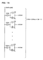
- Fig. 18 shows an example of a detailed configuration of the operational amplifier circuit.
- the operational amplifier circuit shown in Fig. 18 differs from the operational amplifier circuit which has been described in conjunction with Fig. 7A to Fig. 11B with respect to a point that the operational amplifier OP1 includes the N-type transistors NT14 and NT16 and the P-type transistor PT14, while the operational amplifier OP2 includes the P-type transistors PT24 and PT26 and the N-type transistor PT24.
- the N-type transistors NT13 and NT15 having the reference voltage (bias voltage) VB1 connected to gate electrodes thereof and the P-type transistors PT23 and PT25 having the reference voltage (bias voltage) VB2 connected to gate electrodes thereof respectively correspond to the current sources IS11, IS12, IS21 and IS22 in Fig. 8 and Fig. 9.
- RP indicates a resistance for protecting an output of the operational amplifier circuit from static electricity.
- the ON/OFF control of the current sources IS11(NT13), IS12(NT15), IS21(PT23) and IS22(PT25) of the operational amplifiers OP1 and OP2 is performed so as to realize the ON/OFF control of the operations of the operational amplifiers.
- signals OFF1D and OFF1Q are connected to the gate electrodes of the N-type transistors NT14 and NT16, while signals XOFF2D and XOFF2Q are connected to the gate electrodes of the P-type transistors PT24 and PT26. Then, these signals OFF1D, OFF1Q, XOFF2D and XOFF2Q are subjected to a signal control as shown in a timing waveform chart in Fig. 19A, for example.
- 'X' of the signals XOFF2D and XOFF2Q means "negative logic".
- the signals OFF1D and OFF1Q become H level (active) and the N-type transistors NT14 and NT16 in Fig. 18 are turned on. Accordingly, the current flows into the current sources IS11 (NT13) and IS12 (NT15) of the operational amplifier OP1 so that the operational amplifier OP1 is in the operable state.
- the signals XOFF2D and XOFF2Q become H level (non-active) and the P-type transistors PT24 and PT26 are turned off. Accordingly, the current which flows into the current sources IS21(PT23) and IS22(PT25) of the operational amplifier OP2 is cut off so that the operational amplifier OP2 is in the inoperable state.
- the operational amplifier OP2 is set to the inoperable state and hence, the power consumption can be lowered. That is, compared to a case in which both of the operational amplifiers OP1 and OP2 are set to the operable state, the power consumption can be halved. Then, during the period T1, only the output of the operational amplifier OP1 is selected by the selection circuit 70 and the data line S is driven only by the operational amplifier OP1. Accordingly, even when the operational amplifier OP2 becomes the inoperable state during the period T1, there arises no problem with respect to the driving of the data line S.
- the signals OFF1D and OFF1Q become L level (non-active) and the N-type transistors NT14 and NT16 in Fig. 18 are cut off. Accordingly, the current flows into the current sources IS11 and IS12 of the operational amplifier OP1 so that the operational amplifier OP2 becomes the inoperable state.
- the signals XOFF2D and XOFF2Q become L level (active) and the P-type transistors PT24 and PT26 are turned on. Accordingly, the current flows into the current sources IS21 and IS22 of the operational amplifier OP2 so that the operational amplifier OP2 are in the operable state.
- the operational amplifier OP1 is set to the inoperable state and hence, the power consumption can be lowered. That is, compared to a case in which both of the operational amplifiers OP1 and OP2 are set to the operable state, the power consumption can be halved. Then, during the period T2, only the output of the operational amplifier OP2 is selected by the selection circuit 70 and the data line S is driven only by the operational amplifier OP2. Accordingly, even when the operational amplifier OP1 becomes the inoperable state during the period T2, there arises no problem with respect to the driving of the data line S.
- the current sources of the operational amplifier which is not used can be turned off thus succeeding in the lowering of the power consumption of the operational amplifier circuit.
- the signals OFF1D, OFF1Q, XOFF2D and XOFF2Q may be subjected to a signal control shown in a timing waveform chart in Fig. 19B.
- the response speed and the frequency characteristics of the operational amplifier can be enhanced so that the current is large in general. Accordingly, by performing the ON/OFF control of the current which flows in the current sources IS11 and IS21, the more effective lowering of power consumption can be realized.
- the current supply ability (driving ability) is not required so much with respect to the current sources IS12 and IS22 of the output section of the operational amplifier. Accordingly, even when the current which flows in the current sources IS12 and IS22 is not subjected to the ON/OFF control but is always allowed to flow into the current sources IS12 and IS22, the transistors PT13 and NT23 are turned off through the transistors PT14 and NT24 in response to the signals SEL1, SEL2 and hence, the power consumption is not increased so much.
- the voltage levels of the outputs Q1 and Q2 of the operational amplifiers OP1 and OP2 can be made stable and the voltage levels of the outputs Q1 and Q2 can be set to L level (VSS) and H level (VDD) when the driving transistors PT13 and NT23 are in the OFF state. Accordingly, as will be described later, a problem which may arise due to a phenomenon that the voltage level of the outputs Q1, Q2 becomes unstable can be effectively prevented.
- control is performed so as to cut off the electric current which flows in the current sources IS11, IS12, IS21 and IS22 in Fig. 19A and Fig. 19B
- control may be performed so as to restrict or decrease the electric current without completely cutting off the current.
- the ON/OFF control of the driving transistors PT13 and NT23 of the operational amplifiers OP1 and OP2 is performed using the transistors PT14 and NT24 shown in Fig. 18 thus preventing the outputs Q1 and Q2 of the operational amplifiers OP1 and OP2 from becoming unstable.
- the signal SEL1 is connected to the gate electrode of the P-type transistor PT14.
- This signal SEL1 is a signal which is also used for the ON/OFF control of the transfer gate TG1 and instructs the selection/non-selection of the operational amplifier OP1 (see Fig. 11A and Fig. 11B).
- an inversion signal of the signal SEL2 is connected to the gate electrode of the N-type transistor NT24.
- This signal SEL2 is a signal which is also used for the ON/OFF control of the transfer gate TG2 and instructs the selection/non-selection of the operational amplifier OP2.
- the signal SEL1 becomes H level (active) and the transfer gate TG1 in Fig. 18 is turned on. Accordingly, the operational amplifier OP1 is selected and the output Q1 is connected to the data line S.
- the signal SEL2 becomes L level (non-active) and the N-type transistor NT24 to which the inversion signal of the signal SEL2 is inputted is turned on. Accordingly, the signal XDQ2 which is connected to the gate electrode of the driving transistor NT23 becomes L level so that the driving transistor NT23 is turned off. Accordingly, the voltage level of the output Q2 of the operational amplifier OP2 is pulled toward the VDD side due to the current source IS22 and is set to H level. That is, during the period T1 during which the operational amplifier OP2 is in the inoperable state, it is possible to prevent the voltage level of the output Q2 of the operational amplifier OP2 from becoming unstable.
- the signal SEL2 becomes H level (active) and the transfer gate TG2 in Fig. 18 is turned on. Accordingly, the operational amplifier OP2 is selected and the output Q2 is connected to the data line S.
- the signal SEL1 becomes L level (non-active) and the P-type transistor NT14 to which the signal SEL1 is inputted is turned on. Accordingly, the signal XDQ1 which is connected to the gate electrode of the driving transistor PT13 becomes H level so that the driving transistor PT23 is turned off. Accordingly, the voltage level of the output Q1 of the operational amplifier OP1 is pulled toward the VSS side due to the current source IS12 and is set to L level. That is, during the period T2 in which the operational amplifier OP1 is in the inoperable state, it is possible to prevent the voltage level of the output Q1 of the operational amplifier OP1 from becoming unstable.
- the gate electrode of the driving transistor NT23 which the operational amplifier OP2 includes becomes L level so that the driving transistor NT23 is turned off. Since the current source IS22 is always in the ON state at this point of time, the voltage level of the output Q2 of the operational amplifier OP2 is changed to the VDD side and becomes H level.
- the data line S (output of the operational amplifier circuit) is set to the high impedance state as indicated by E3 in Fig. 20. Then, by changing the counter electrode VCOM from VC1 to VC2 in this high impedance state, the voltage level of the data line S is elevated as described in conjunction with B3 in Fig. 17.
- the driving transistor NT23 of the operational amplifier OP2 is turned off as indicated by E1 in Fig. 20 and the output Q2 of the operational amplifier OP2 becomes H level and hence, the adverse influence caused by the redistribution of charge can be minimized thus preventing the above-mentioned phenomenon.
- the gate electrode of the driving transistor PT13 which the operational amplifier OP1 includes becomes H level so that the driving transistor PT13 is turned off. Since the current source IS12 is always in the ON state at this point of time, the voltage level of the output Q1 of the operational amplifier OP1 is changed to the VSS side and becomes L level.
- the data line S before driving the data line S using the operational amplifier OP1, the data line S is set to the high impedance state as indicated by E13 in Fig. 20. Then, by changing the voltage level of the counter electrode VCOM from VC2 to VC1 in this high impedance state, the voltage level of the data line S is lowered as described in conjunction with B13 in Fig. 17.
- the driving transistor PT13 of the operational amplifier OP1 is turned off as indicated by E11 in Fig. 20 and the output Q2 of the operational amplifier OP1 becomes L level and hence, the adverse influence caused by the redistribution of charge can be minimized thus preventing the above-mentioned phenomenon.
- this embodiment performs a high impedance control of the output Q of the operational amplifier circuit and provides a clamp circuit 80 to the output Q.
- this clamp circuit 80 the output Q (data line S) of the operational amplifier circuit is clamped in a voltage range equal to or wider than a voltage range between the power sources VDD, VSS of the operational amplifier circuit. Accordingly, it is possible to return the excessive charge to the power source VDD side or the power source VSS side so that the power consumption of the liquid crystal device can be lowered.
- the clamp circuit 80 includes a diode DI1 (clamp element) which is inserted between the power source VSS (second power source) and the data line S and a diode DI2 which is inserted between the data line S and the power source VDD (first power source).
- the diode DI1 is a diode which sets the direction advancing from the power source VSS to the data line S as the forward direction
- the diode DI2 is a diode which sets the direction advancing from the data line S to the power source VDD as the forward direction.
- Fig. 21B shows an example of the element structure of the diode DI1 provided to the VSS side.
- the diode DI1 uses a p well region p - which is connected to the power source VSS through an active region p + as a positive-polarity-side electrode and an active region n + as a negative-polarity-side electrode.
- Fig. 21C shows an example of the element structure of the diode DI2 provided to the VDD side.
- the diode DI2 uses an active region p + as a positive-polarity-side electrode and an n well region n - which is connected to the power source VDD through an active region n + as a negative-polarity-side electrode.
- diodes DI1 and DI2 can be also used as protective circuits for the operational amplifier circuit. More specifically, these diodes DI1 and DI2 may be incorporated into an I/O circuit (I/O pad) of a semiconductor device in which the operational amplifier circuit (driving circuit) is formed.
- the diode may be provided to only one side.
- the output transistors (transfer gates TG1 and TG2 in Fig. 18, for example) of the operational amplifier circuit may be used as the diodes DI1 and DI2 (clamp circuit).
- the written voltage VS (gray scale voltage) of the data line S is 3V when the counter electrode VCOM is 0V as indicated by F1 in Fig. 22A.
- the counter electrode VCOM is changed from 0V (VC1) to 5V(VC2) as indicated by F1 and F2 in Fig. 22A in this state.
- the output of the operational amplifier circuit is set to the high impedance state (see Fig. 10 to Fig. 11B)
- the parasitic capacitance CPA generated between the counter electrode VCOM and the data line S see Fig. 16
- 0.6V is the forward direction voltage of PN junction of the diode.
- the power source for the operational amplifier circuit and the power source for the clamp circuit are provided as circuits different from each other.
- the power sources of the operational amplifier circuit are constituted of power sources VDD and VSS (first and second power sources) and the power sources of the clamp circuit are constituted of power sources VDD' and VSS' (third and fourth power sources)
- VDD - VSS > VDD' - VSS' is established. That is, the voltage range of the power sources VDD' and VSS' of the clamp circuit is set narrower than the voltage range of the power sources VDD and VSS of the operational amplifier circuit. For example, when the voltage range of VDD and VSS is 5V to 0V, the voltage range of VDD' and VSS' is set to 4.4V to 0.6V.
- the power sources VDD' and VSS' of the clamp circuit can be generated by utilizing the voltage generation function (gray scale voltage generation function) of the power source circuit 42 in Fig. 1.
- VDD' ⁇ VDD - VBD, VSS' ⁇ VSS + VBD is established.
- VDD' > 4.4V, VSS' ⁇ 0.6V is established.
- the power consumption lowering method which includes setting the output of the operational amplifier circuit to the high impedance state when the voltage level of the counter electrode VCOM is changed over and providing the clamp circuit to the output of the operational amplifier circuit is also effectively applicable to the AB class operational amplifier circuit shown in Fig. 6. That is, also with respect to the AB class operational amplifier circuit, the excessive charge can be returned to the power source side and the power consumption can be lowered by an amount corresponding to the excessive charge.
- the polarity of voltage applied to the liquid crystal element is inverted every scanning period (scan line) and is also inverted every frame. Accordingly, it is possible to prevent the phenomenon that the direct current voltage is applied to the liquid display element for a long time so that the deterioration of the liquid crystal element can be prevented.
- the (M - 1) th scanning period (the period in which the (M - 1) th scan line is selected) as shown in Fig. 24, VCOM becomes VC1 and VC1 is lower than the gray scale voltage and hence, the (M - 1) th scanning period becomes the period T1 in which the voltage applied to the liquid crystal element has the positive polarity.
- the final Mth scanning period (the period in which the Mth scan line is selected)
- VCOM becomes VC2 and VC2 is higher than the gray scale voltage and hence, the Mth scanning period becomes the period T2 in which the voltage applied to the liquid crystal element has the negative polarity.
- the first scanning period (the period in which the first scan line is selected) of the next frame, VCOM becomes VC1 and hence, the first scanning period becomes the period T2 in which the voltage applied to the liquid crystal element has the negative polarity.
- both of the Mth scanning period and the first scanning period of the next frame are periods T of negative polarity and hence, even when the scanning period is changed from the Mth scanning period to the first scanning period, VCOM is held at VC2 as indicated by K1 and the polarity is not inverted. Further, in the Mth scanning period as well as in the first scanning period, the data line is driven by the N-type operational amplifier OP2.
- the direction that the voltage level of the data line is changed depends on the gray scale level (see A1 to A4 in Fig. 5) and it is difficult to specify the direction to one direction. Accordingly, when the data line is driven by the N-type operational amplifier OP2 as indicated by K3 in Fig. 24 in the first scanning period, there arises a case in which it is necessary to spend a long time until the voltage level of the data line is set to the voltage level corresponding to the gray scale level. This is because that when the direction that the voltage level of the data line is changed is set to the VDD side, it is necessary to drive the data line using the current source IS22 in Fig. 9 which exhibits the low current supply ability.
- the display panel (electro-optical device) is driven by the scan line inversion driving (inversion driving which sets the voltage level of the counter electrode VCOM during the scanning period to the voltage level which is different from the voltage level of the preceding scanning period) shown in Fig. 23.
- the scan line inversion driving inversion driving which sets the voltage level of the counter electrode VCOM during the scanning period to the voltage level which is different from the voltage level of the preceding scanning period
- the driving is performed while setting VCOM to VC2 (either one voltage level of VC1 and VC2 in a broad sense).
- the virtual (dummy) scanning period is provided next to the Mth scanning period.
- the driving is performed while setting VCOM to VC1 (the other voltage level different from the above-mentioned one voltage level in a broad sense). That is, the counter electrode VCOM is subjected to the inversion of polarity.
- the operational amplifier is changed over from the operational amplifier OP1 (P type) to the operational amplifier OP2 (N type), from the operational amplifier OP2 to the operational amplifier OP1, and from the operational amplifier OP1 (P type) to the operational amplifier OP2 (N type) sequentially. That is, the driving is performed during the scanning period using the operational amplifier different from the operational amplifier used in the preceding scanning period.
- the output (data line) of the operational amplifier circuit is set to the high impedance state.
- the data line is driven using the operational amplifier corresponding to the polarity of the period.
- the virtual scanning period is the period T1 of positive polarity at L2 in Fig. 25 and hence, the data line is driven using the P-type operational amplifier OP1 which has the high ability to change the voltage level to the VDD side.
- the virtual scanning period is the period T2 of negative polarity
- the data line is driven using the N-type operational amplifier OP2 having the high ability to change the voltage level to the VSS side.
- the scan line driving circuit 30 shown in Fig. 1 does not drive the scan lines G1 to GM but performs the virtual driving of virtual scan lines.
- the controller 40 shown in Fig. 1 inputs the enable input/output signal EIO shown in Fig. 3 to the shift resister 32 not every 228 scanning period but every 229 scanning period. Due to such an operation, during the virtual scanning period which comes next to the Mth scanning period, the enable input/output signal EIO is not present in the shift resister 32 so that the driving of the actual scan lines is not performed.
- the method which provides the virtual scanning periods as shown in Fig. 25 is also applicable to a driving method in which one frame is divided into a plurality of driving fields.
- the method shown in Fig. 25 is also applicable to a driving method in which an additional transistor (pre-charge transistor, for example) is provided to the output of the operational amplifier circuit and the voltage level of the data line is changed before driving.
- an additional transistor pre-charge transistor, for example
- the liquid crystal device to which the present invention is applicable is not limited to such a liquid crystal device.
- the configuration of the operational amplifier circuit is not limited to the configuration which has been described in this embodiment.
- the present invention is not limited to the liquid crystal device (LCD panel) and is also applicable to an electro-luminescence (EL) device, an organic EL device and a plasma display device.
- EL electro-luminescence
- the present invention is not limited to the scan line inversion driving and is also applicable to other inversion driving methods.
Applications Claiming Priority (2)
| Application Number | Priority Date | Filing Date | Title |
|---|---|---|---|
| JP2001168519A JP3820918B2 (ja) | 2001-06-04 | 2001-06-04 | 演算増幅回路、駆動回路、及び駆動方法 |
| JP2001168519 | 2001-06-04 |
Publications (3)
| Publication Number | Publication Date |
|---|---|
| EP1265216A2 true EP1265216A2 (de) | 2002-12-11 |
| EP1265216A3 EP1265216A3 (de) | 2004-01-02 |
| EP1265216B1 EP1265216B1 (de) | 2007-03-14 |
Family
ID=19010737
Family Applications (1)
| Application Number | Title | Priority Date | Filing Date |
|---|---|---|---|
| EP02012195A Expired - Fee Related EP1265216B1 (de) | 2001-06-04 | 2002-06-03 | Operationelle Verstärkerschaltung, Treiberschaltung und -Verfahren |
Country Status (7)
| Country | Link |
|---|---|
| US (1) | US7006070B2 (de) |
| EP (1) | EP1265216B1 (de) |
| JP (1) | JP3820918B2 (de) |
| KR (1) | KR100523884B1 (de) |
| CN (1) | CN1183405C (de) |
| DE (1) | DE60218781T2 (de) |
| TW (1) | TWI231468B (de) |
Cited By (3)
| Publication number | Priority date | Publication date | Assignee | Title |
|---|---|---|---|---|
| EP1265217A2 (de) * | 2001-06-04 | 2002-12-11 | Seiko Epson Corporation | Operationelle Verstärkerschaltung, Treiberschaltung und -Verfahren |
| DE102004050392B4 (de) * | 2003-12-29 | 2008-08-07 | Lg. Philips Lcd Co., Ltd. | Treibersystem für eine Flüssigkristallanzeige |
| EP2075790A2 (de) * | 2007-12-27 | 2009-07-01 | BYD Company Limited | TFT-LCD-Treiberschaltung und LCD-Vorrichtungen |
Families Citing this family (25)
| Publication number | Priority date | Publication date | Assignee | Title |
|---|---|---|---|---|
| JP3871659B2 (ja) * | 2003-06-25 | 2007-01-24 | ローム株式会社 | 電源回路 |
| JP4049140B2 (ja) * | 2004-09-03 | 2008-02-20 | セイコーエプソン株式会社 | インピーダンス変換回路、駆動回路及び制御方法 |
| CN100389449C (zh) * | 2005-02-18 | 2008-05-21 | 奇景光电股份有限公司 | 源极驱动器及其驱动方法 |
| JP4419897B2 (ja) * | 2005-03-30 | 2010-02-24 | エプソンイメージングデバイス株式会社 | 液晶表示装置の駆動法、液晶表示装置及び電子機器 |
| JP4887657B2 (ja) * | 2005-04-27 | 2012-02-29 | 日本電気株式会社 | アクティブマトリクス型表示装置及びその駆動方法 |
| JP4840908B2 (ja) * | 2005-12-07 | 2011-12-21 | ルネサスエレクトロニクス株式会社 | 表示装置駆動回路 |
| KR100806122B1 (ko) | 2006-05-02 | 2008-02-22 | 삼성전자주식회사 | 소스 구동회로, 데이터 라인 구동 방법 및 액정 표시 장치 |
| KR101361083B1 (ko) * | 2006-10-23 | 2014-02-13 | 삼성디스플레이 주식회사 | 데이터 구동 장치와 이를 포함하는 액정 표시 장치 및 액정표시 장치의 구동 방법 |
| TWI345093B (en) * | 2006-11-10 | 2011-07-11 | Chimei Innolux Corp | Method of manufacturing liquid crystal display |
| JP4873760B2 (ja) * | 2007-03-16 | 2012-02-08 | シャープ株式会社 | 液晶表示装置およびその駆動方法 |
| US9196206B2 (en) * | 2007-04-26 | 2015-11-24 | Sharp Kabushiki Kaisha | Liquid crystal display |
| CN101329484B (zh) * | 2007-06-22 | 2010-10-13 | 群康科技(深圳)有限公司 | 液晶显示装置之驱动电路及其驱动方法 |
| WO2010001590A1 (ja) * | 2008-07-04 | 2010-01-07 | パナソニック株式会社 | 表示装置及びその制御方法 |
| JP5266084B2 (ja) * | 2009-02-17 | 2013-08-21 | ルネサスエレクトロニクス株式会社 | 過電流保護回路 |
| JP4883113B2 (ja) * | 2009-03-06 | 2012-02-22 | セイコーエプソン株式会社 | 集積回路装置、電気光学装置及び電子機器 |
| JP5775357B2 (ja) * | 2010-05-21 | 2015-09-09 | 株式会社半導体エネルギー研究所 | 液晶表示装置 |
| JP5679172B2 (ja) | 2010-10-29 | 2015-03-04 | 株式会社ジャパンディスプレイ | 液晶表示装置 |
| US8878608B2 (en) * | 2011-11-03 | 2014-11-04 | Mediatek Inc. | Comparator and amplifier |
| KR102052644B1 (ko) * | 2013-05-27 | 2020-01-09 | 삼성디스플레이 주식회사 | 표시 장치 및 그 구동 방법 |
| TWI508049B (zh) * | 2013-07-29 | 2015-11-11 | Himax Tech Ltd | 源極驅動器 |
| CN107507588A (zh) * | 2017-08-28 | 2017-12-22 | 惠科股份有限公司 | 显示面板的驱动电路及驱动方法 |
| US10878738B1 (en) | 2019-07-30 | 2020-12-29 | Wuhan China Star Optoelectronics Semiconductor Display Technology Co., Ltd. | Display product and drive chip for driving display panel |
| CN110491344B (zh) * | 2019-07-30 | 2020-11-06 | 武汉华星光电半导体显示技术有限公司 | 用于驱动显示面板的驱动芯片及显示产品 |
| US11196397B2 (en) * | 2019-12-31 | 2021-12-07 | Novatek Microelectronics Corp. | Current integrator for OLED panel |
| KR20220012546A (ko) * | 2020-07-23 | 2022-02-04 | 주식회사 엘엑스세미콘 | 디스플레이 구동 장치 |
Citations (6)
| Publication number | Priority date | Publication date | Assignee | Title |
|---|---|---|---|---|
| GB2188471A (en) * | 1986-03-19 | 1987-09-30 | Sharp Kk | L C D devices |
| EP0548051A2 (de) * | 1986-09-25 | 1993-06-23 | The Board of Trustees of the University of Illinois | Verfahren und Schaltung zur Erhaltung von Zellen und Bildelementen von Plasma-Anzeigen, Elektrolumineszenz-Anzeigen, Flüssigkristall- oder ähnlichen Anzeigen |
| EP0711033A1 (de) * | 1994-10-31 | 1996-05-08 | STMicroelectronics S.r.l. | In verschiedene Konfigurationen umschaltbarer Operationsverstärker |
| US6172663B1 (en) * | 1995-03-14 | 2001-01-09 | Sharp Kabushiki Kaisha | Driver circuit |
| EP1265215A2 (de) * | 2001-06-04 | 2002-12-11 | Seiko Epson Corporation | Schaltung und Verfahren zur Ansteuerung der Gegenelektrode einer Flüssigkristallanzeigetafel |
| EP1265217A2 (de) * | 2001-06-04 | 2002-12-11 | Seiko Epson Corporation | Operationelle Verstärkerschaltung, Treiberschaltung und -Verfahren |
Family Cites Families (24)
| Publication number | Priority date | Publication date | Assignee | Title |
|---|---|---|---|---|
| US5898762A (en) | 1985-07-10 | 1999-04-27 | Ronald A. Katz Technology Licensing, L.P. | Telephonic-interface statistical analysis system |
| US5059921A (en) | 1990-07-27 | 1991-10-22 | Motorola Inc. | Amplifier having two operating modes |
| JP2695981B2 (ja) * | 1990-10-05 | 1998-01-14 | 株式会社東芝 | 液晶表示器駆動電源回路 |
| JPH0523676A (ja) | 1991-07-25 | 1993-02-02 | Konica Corp | 廃液の処理方法および装置 |
| JP3088821B2 (ja) | 1992-03-18 | 2000-09-18 | 沖電気工業株式会社 | パワーオンリセット回路 |
| JP2872511B2 (ja) * | 1992-12-28 | 1999-03-17 | シャープ株式会社 | 表示装置の共通電極駆動回路 |
| US5361041A (en) * | 1993-06-17 | 1994-11-01 | Unitrode Corporation | Push-pull amplifier |
| JP3329077B2 (ja) | 1993-07-21 | 2002-09-30 | セイコーエプソン株式会社 | 電源供給装置、液晶表示装置及び電源供給方法 |
| JPH07281639A (ja) | 1994-04-11 | 1995-10-27 | Oki Electric Ind Co Ltd | アクティブマトリクス型液晶ディスプレイの階調駆動方法及びアクティブマトリクス型液晶ディスプレイ |
| JPH07281640A (ja) | 1994-04-11 | 1995-10-27 | Oki Electric Ind Co Ltd | アクティブマトリクス型液晶ディスプレイの階調駆動方法及びアクティブマトリクス型液晶ディスプレイ |
| US5528256A (en) * | 1994-08-16 | 1996-06-18 | Vivid Semiconductor, Inc. | Power-saving circuit and method for driving liquid crystal display |
| JPH08272339A (ja) * | 1995-04-04 | 1996-10-18 | Hitachi Ltd | 液晶表示装置 |
| JPH09230829A (ja) | 1996-02-26 | 1997-09-05 | Oki Electric Ind Co Ltd | ソースドライバの出力回路 |
| JP3435292B2 (ja) * | 1996-08-29 | 2003-08-11 | 富士通株式会社 | オペアンプ回路 |
| US5850139A (en) * | 1997-02-28 | 1998-12-15 | Stmicroelectronics, Inc. | Load pole stabilized voltage regulator circuit |
| KR100284024B1 (ko) | 1997-07-29 | 2001-03-02 | 윤종용 | 저전압 씨모오스 연산 증폭기 회로 및 그것을 구비한 샘플 앤드 홀드 회로 |
| JP3613940B2 (ja) * | 1997-08-29 | 2005-01-26 | ソニー株式会社 | ソースフォロワ回路、液晶表示装置および液晶表示装置の出力回路 |
| JP3228411B2 (ja) | 1998-03-16 | 2001-11-12 | 日本電気株式会社 | 液晶表示装置の駆動回路 |
| JP3622516B2 (ja) | 1998-07-10 | 2005-02-23 | カシオ計算機株式会社 | 液晶駆動装置 |
| JP3914639B2 (ja) * | 1998-07-13 | 2007-05-16 | 株式会社アドバンスト・ディスプレイ | 液晶表示装置 |
| JP3317263B2 (ja) * | 1999-02-16 | 2002-08-26 | 日本電気株式会社 | 表示装置の駆動回路 |
| JP3527168B2 (ja) * | 1999-06-02 | 2004-05-17 | シャープ株式会社 | 液晶表示装置 |
| JP2001004974A (ja) * | 1999-06-18 | 2001-01-12 | Sanyo Electric Co Ltd | 液晶駆動回路 |
| JP2001125543A (ja) * | 1999-10-27 | 2001-05-11 | Nec Corp | 液晶駆動回路 |
-
2001
- 2001-06-04 JP JP2001168519A patent/JP3820918B2/ja not_active Expired - Fee Related
-
2002
- 2002-05-29 US US10/155,972 patent/US7006070B2/en not_active Expired - Fee Related
- 2002-05-31 TW TW091111762A patent/TWI231468B/zh not_active IP Right Cessation
- 2002-06-03 DE DE60218781T patent/DE60218781T2/de not_active Expired - Lifetime
- 2002-06-03 EP EP02012195A patent/EP1265216B1/de not_active Expired - Fee Related
- 2002-06-04 KR KR10-2002-0031277A patent/KR100523884B1/ko not_active IP Right Cessation
- 2002-06-04 CN CNB021222576A patent/CN1183405C/zh not_active Expired - Fee Related
Patent Citations (6)
| Publication number | Priority date | Publication date | Assignee | Title |
|---|---|---|---|---|
| GB2188471A (en) * | 1986-03-19 | 1987-09-30 | Sharp Kk | L C D devices |
| EP0548051A2 (de) * | 1986-09-25 | 1993-06-23 | The Board of Trustees of the University of Illinois | Verfahren und Schaltung zur Erhaltung von Zellen und Bildelementen von Plasma-Anzeigen, Elektrolumineszenz-Anzeigen, Flüssigkristall- oder ähnlichen Anzeigen |
| EP0711033A1 (de) * | 1994-10-31 | 1996-05-08 | STMicroelectronics S.r.l. | In verschiedene Konfigurationen umschaltbarer Operationsverstärker |
| US6172663B1 (en) * | 1995-03-14 | 2001-01-09 | Sharp Kabushiki Kaisha | Driver circuit |
| EP1265215A2 (de) * | 2001-06-04 | 2002-12-11 | Seiko Epson Corporation | Schaltung und Verfahren zur Ansteuerung der Gegenelektrode einer Flüssigkristallanzeigetafel |
| EP1265217A2 (de) * | 2001-06-04 | 2002-12-11 | Seiko Epson Corporation | Operationelle Verstärkerschaltung, Treiberschaltung und -Verfahren |
Cited By (4)
| Publication number | Priority date | Publication date | Assignee | Title |
|---|---|---|---|---|
| EP1265217A2 (de) * | 2001-06-04 | 2002-12-11 | Seiko Epson Corporation | Operationelle Verstärkerschaltung, Treiberschaltung und -Verfahren |
| EP1265217A3 (de) * | 2001-06-04 | 2004-01-28 | Seiko Epson Corporation | Operationelle Verstärkerschaltung, Treiberschaltung und -Verfahren |
| DE102004050392B4 (de) * | 2003-12-29 | 2008-08-07 | Lg. Philips Lcd Co., Ltd. | Treibersystem für eine Flüssigkristallanzeige |
| EP2075790A2 (de) * | 2007-12-27 | 2009-07-01 | BYD Company Limited | TFT-LCD-Treiberschaltung und LCD-Vorrichtungen |
Also Published As
| Publication number | Publication date |
|---|---|
| US7006070B2 (en) | 2006-02-28 |
| DE60218781D1 (de) | 2007-04-26 |
| TWI231468B (en) | 2005-04-21 |
| JP2002366105A (ja) | 2002-12-20 |
| JP3820918B2 (ja) | 2006-09-13 |
| DE60218781T2 (de) | 2007-12-06 |
| EP1265216A3 (de) | 2004-01-02 |
| KR100523884B1 (ko) | 2005-10-26 |
| CN1389842A (zh) | 2003-01-08 |
| US20020180717A1 (en) | 2002-12-05 |
| KR20020092825A (ko) | 2002-12-12 |
| EP1265216B1 (de) | 2007-03-14 |
| CN1183405C (zh) | 2005-01-05 |
Similar Documents
| Publication | Publication Date | Title |
|---|---|---|
| EP1265215A2 (de) | Schaltung und Verfahren zur Ansteuerung der Gegenelektrode einer Flüssigkristallanzeigetafel | |
| EP1265216B1 (de) | Operationelle Verstärkerschaltung, Treiberschaltung und -Verfahren | |
| EP1265217B1 (de) | Operationelle Verstärkerschaltung, Treiberschaltung und -Verfahren | |
| US8125432B2 (en) | Common voltage generation circuit employing a charge-pump operation to generate low-potential-side voltage | |
| JP3520418B2 (ja) | 演算増幅回路、駆動回路及び演算増幅回路の制御方法 | |
| TWI386897B (zh) | 源極驅動器、光電裝置、及電子機器 | |
| KR100894188B1 (ko) | 구동 회로, 전기 광학 장치 및 전자 기기 | |
| US20070290979A1 (en) | Source drive amplifier for flat panel display | |
| US8558852B2 (en) | Source driver, electro-optical device, and electronic instrument | |
| JP4543964B2 (ja) | コモン電圧生成回路、電源回路、表示ドライバ及び表示装置 | |
| JP3888350B2 (ja) | 演算増幅器及びこれを用いた駆動回路 | |
| US8605070B2 (en) | Operational amplifier and display panel driving device | |
| JP4858250B2 (ja) | コモン電圧生成回路、電源回路、表示ドライバ及びコモン電圧生成方法 | |
| KR20050096999A (ko) | 감마회로 및 이를 내장한 액정표시장치 |
Legal Events
| Date | Code | Title | Description |
|---|---|---|---|
| PUAI | Public reference made under article 153(3) epc to a published international application that has entered the european phase |
Free format text: ORIGINAL CODE: 0009012 |
|
| AK | Designated contracting states |
Kind code of ref document: A2 Designated state(s): AT BE CH CY DE DK ES FI FR GB GR IE IT LI LU MC NL PT SE TR |
|
| AX | Request for extension of the european patent |
Free format text: AL;LT;LV;MK;RO;SI |
|
| PUAL | Search report despatched |
Free format text: ORIGINAL CODE: 0009013 |
|
| AK | Designated contracting states |
Kind code of ref document: A3 Designated state(s): AT BE CH CY DE DK ES FI FR GB GR IE IT LI LU MC NL PT SE TR |
|
| AX | Request for extension of the european patent |
Extension state: AL LT LV MK RO SI |
|
| 17P | Request for examination filed |
Effective date: 20040604 |
|
| 17Q | First examination report despatched |
Effective date: 20040719 |
|
| AKX | Designation fees paid |
Designated state(s): DE GB |
|
| GRAP | Despatch of communication of intention to grant a patent |
Free format text: ORIGINAL CODE: EPIDOSNIGR1 |
|
| GRAS | Grant fee paid |
Free format text: ORIGINAL CODE: EPIDOSNIGR3 |
|
| GRAA | (expected) grant |
Free format text: ORIGINAL CODE: 0009210 |
|
| AK | Designated contracting states |
Kind code of ref document: B1 Designated state(s): DE GB |
|
| REG | Reference to a national code |
Ref country code: GB Ref legal event code: FG4D |
|
| REF | Corresponds to: |
Ref document number: 60218781 Country of ref document: DE Date of ref document: 20070426 Kind code of ref document: P |
|
| PLBE | No opposition filed within time limit |
Free format text: ORIGINAL CODE: 0009261 |
|
| STAA | Information on the status of an ep patent application or granted ep patent |
Free format text: STATUS: NO OPPOSITION FILED WITHIN TIME LIMIT |
|
| 26N | No opposition filed |
Effective date: 20071217 |
|
| GBPC | Gb: european patent ceased through non-payment of renewal fee |
Effective date: 20070614 |
|
| PG25 | Lapsed in a contracting state [announced via postgrant information from national office to epo] |
Ref country code: GB Free format text: LAPSE BECAUSE OF NON-PAYMENT OF DUE FEES Effective date: 20070614 |
|
| PGFP | Annual fee paid to national office [announced via postgrant information from national office to epo] |
Ref country code: DE Payment date: 20130529 Year of fee payment: 12 |
|
| REG | Reference to a national code |
Ref country code: DE Ref legal event code: R119 Ref document number: 60218781 Country of ref document: DE |
|
| REG | Reference to a national code |
Ref country code: DE Ref legal event code: R119 Ref document number: 60218781 Country of ref document: DE Effective date: 20150101 |
|
| PG25 | Lapsed in a contracting state [announced via postgrant information from national office to epo] |
Ref country code: DE Free format text: LAPSE BECAUSE OF NON-PAYMENT OF DUE FEES Effective date: 20150101 |