EP1237307A2 - Récepteur et méthode pour détecter, mesurer et compenser la dégradation de la forme d'onde d'un signal reçu - Google Patents
Récepteur et méthode pour détecter, mesurer et compenser la dégradation de la forme d'onde d'un signal reçu Download PDFInfo
- Publication number
- EP1237307A2 EP1237307A2 EP01120687A EP01120687A EP1237307A2 EP 1237307 A2 EP1237307 A2 EP 1237307A2 EP 01120687 A EP01120687 A EP 01120687A EP 01120687 A EP01120687 A EP 01120687A EP 1237307 A2 EP1237307 A2 EP 1237307A2
- Authority
- EP
- European Patent Office
- Prior art keywords
- waveform
- received signal
- sampling
- received
- data
- Prior art date
- Legal status (The legal status is an assumption and is not a legal conclusion. Google has not performed a legal analysis and makes no representation as to the accuracy of the status listed.)
- Ceased
Links
Images


Classifications
-
- H—ELECTRICITY
- H04—ELECTRIC COMMUNICATION TECHNIQUE
- H04B—TRANSMISSION
- H04B10/00—Transmission systems employing electromagnetic waves other than radio-waves, e.g. infrared, visible or ultraviolet light, or employing corpuscular radiation, e.g. quantum communication
- H04B10/25—Arrangements specific to fibre transmission
- H04B10/2507—Arrangements specific to fibre transmission for the reduction or elimination of distortion or dispersion
- H04B10/2513—Arrangements specific to fibre transmission for the reduction or elimination of distortion or dispersion due to chromatic dispersion
-
- H—ELECTRICITY
- H04—ELECTRIC COMMUNICATION TECHNIQUE
- H04B—TRANSMISSION
- H04B2210/00—Indexing scheme relating to optical transmission systems
- H04B2210/25—Distortion or dispersion compensation
- H04B2210/252—Distortion or dispersion compensation after the transmission line, i.e. post-compensation
Definitions
- the present invention relates to a receiving apparatus and a method of compensating for waveform degradation of received signals, and further to an apparatus and method for detecting waveform degradation, and an apparatus and method for measuring waveforms. More particularly, the invention relates to a technique suitable for use in compensation for waveform degradation an optical signal suffers due to an optical transmission line.
- FIG. 20 is a block diagram showing one example of the existing optical transmitting system.
- an optical transmission system 100 is made up of an optical transmission apparatus 200, an optical repeater (optical amplifier) 300, and an optical receiving apparatus 400, with an optical signal sent from the optical transmitting apparatus 200 being transmitted through an optical transmission line 500 to the optical receiving apparatus 400 while being repeated/amplified properly in the optical repeater 300.
- an optical repeater 300 exists in the illustration of FIG. 20, naturally, two or more optical repeaters are employable, or no need therefor arises, depending on an optical signal transmission distance.
- the optical transmission line 500 there has frequently been used a single-mode optical fiber (SMF) of a wavelength (referred to as "zero dispersion wavelength") at which chromatic dispersion becomes almost zero being in a 1.3- ⁇ m (micrometer) band (see a chromatic dispersion characteristic 600 in FIG. 22).
- the "chromatic dispersion” signifies the property that the propagation speed in an optical fiber varies with optical wavelength, stemming from material dispersion (see a broken line 800 in FIG. 22) or structure (waveguide) dispersion (see a chain line 900 in FIG. 22) of the optical fiber itself (that is, with respect to the zero dispersion wavelength, the long wavelength side delays while the short wavelength side advances).
- the zero dispersion wavelength means a wavelength at which no advance nor delay occurs while light (wavelength) propagates in an optical fiber.
- the reason for the frequent use of SMF as the optical transmission line 500 is because its transmission loss is at a minimum in an optical transmission band (1.55- ⁇ m band) put frequently to use for the WDM optical transmission, and long-distance transmission is feasible.
- the employment of SMF causes the waveform degradation arising from the chromatic dispersion to occur remarkably at high-speed transmission of an optical signal.
- the waveform degradation arising from the chromatic dispersion includes a case (see FIG. 21B) in which the eye aperture in the amplitude direction becomes smaller (waveform is rounded) as compared with the original transmission waveform (see FIG. 21A) and a case (see FIG. 21C) in which the eye aperture in the phase direction decreases (phase is compressed) with respect to the original transmission waveform.
- the difference therebetween depends upon the designs (type of the optical transmission line 500, optical transmission band, chirping setting, and others) on the optical transmission system.
- the chirping setting is made such that the rise of the waveform is at the short-wavelength side (the fall is at the long-wavelength side)
- the long-wavelength side intensively receives the effect of the chromatic dispersion so that the waveform tends to be rounded. If the chirping setting is made conversely, then the adverse tendency arises.
- the optical transmission line 500 suffers, has been put at the former stage of the optical receiver 402 as shown in FIG. 20 for compensating for the waveform degradation and enlarging the eye aperture.
- DCF dispersion compensation fiber
- the degree of deterioration of the eye aperture acceptable to the optical receiver 402, i.e., the range of chromatic dispersion value permissible to the optical receiver 402, is restricted by the reception sensitivity characteristic of the optical receiver 402, and the chromatic dispersion value increases in proportion to the transmission distance (see FIG. 22) ; therefore, in the above-mentioned existing optical transmission system 100, there is a need to place the dispersion compensation fiber 401 having a different chromatic dispersion characteristic according to optical transmission distance (repeating distance) to show the range of chromatic dispersion value acceptable to the optical receiver 402.
- the system sacrifices the flexibility and the needed type of dispersion compensation fiber 401 increases, which raises the cost at the system construction and the management cost after the system construction.
- the improvement of the reception sensitivity characteristic of the optical receiver 402 by compensating fixedly for the chromatic dispersion through the use of the dispersion compensation fiber 401 as mentioned above encounters limitation even from the viewpoint of ultra-high speed and vary-large capacity required in the recent WDM transmission technology, and the difficulty of coping with the further increase in speed and capacity in the future is easily predictable.
- the present invention has been developed with a view to eliminating the above-mentioned problems, and it is therefore an object of the invention to achieve secure compensation for the waveform degradation of a received signal arising from chromatic dispersion or the like without using a dispersion compensation fiber.
- a receiving apparatus is characterized by comprising the following means:
- received waveform data is measured and the compensation characteristic of the waveform degradation compensating means is controlled so that the difference between the frequency data obtained by converting the measured received waveform data into a frequency domain and the frequency data on the reference waveform shows a minimum; therefore, for example, without the use of a waveform degradation compensator having a different compensation characteristic according to transmission distance of a reception signal, one type of receiving apparatus can cope with the waveform degradation because of the enlargement of the allowable range of the waveform degradation in the receiving apparatus.
- the frequency data in the frequency domain of the received signal is compared with the frequency data on the reference waveform to calculate a difference therebetween, which can cope with every waveform degradation.
- the present invention provides the following advantages.
- the aforesaid received waveform measuring means is composed of an equivalent-time sampling section for equivalent-time-sampling a received signal to acquire a plurality of wave-height data on the received signal and a wave-height data recording section for recording, as received waveform data, the wave-height data acquired by the equivalent-time sampling section. This can securely record/measure the received waveform data through the equivalent-time sampling even if the received signal is a high-speed signal.
- the recording/measurement of the received waveform data is surely feasible regardless of whether or not the received signal is a high-speed signal, so a receiving apparatus is realizable which is capable of implementing sufficient compensation control on a high-speed signal.
- the aforesaid equivalent-time sampling section is composed of a sampling timing generating circuit for generating a sampling timing on the basis of a reference clock synchronized with the received signal to output the sampling timing while shifting a timing of output thereof periodically, and a sampling circuit for sampling the received signal in accordance with the sampling timing generated in the sampling timing generating circuit to acquire the aforesaid wave-height data. This can surely realize the waveform measurement according to the equivalent-time sampling.
- the sampling timing generating circuit includes a divider for dividing the reference clock down and a delay control circuit for supplying the output of the divider to the sampling circuit while delaying periodically. This can generate the sampling timing with a proper operating clock at all times in the apparatus irrespective of the rate (frequency) of the reference clock. Moreover, even in the case of the employment of a divider designed to perform the dividing down into integer (N) times, the sampling timing can be outputted at an arbitrary timing through the delay control by the delay control circuit.
- control means includes the following sections:
- the aforesaid waveform degradation compensating means is constructed with an equalization amplifier having a variable frequency/phase characteristic as the aforesaid compensation characteristic, then it is possible to surely realize the waveform degradation compensation of a received signal (enlargement of the waveform degradation allowable range of the receiving apparatus), which contributes greatly to the realization of this receiving apparatus.
- the equalization amplifier is made up of a plurality of band-pass filters having different pass bands with respect to the received signal, a plurality of phase shifters and a plurality of gain-variable amplifiers, then it is possible to provide an equalization amplifier capable of adjusting the frequency characteristic (amplitude and phase) at every pass band, thus realizing the waveform degradation compensation based on the equalization amplifier with high accuracy.
- the received signal is a signal which is received through an optical transmission line and undergoes waveform degradation based on a chromatic dispersion characteristic of the optical transmission line as the aforesaid waveform degradation
- the waveform degradation compensating means is constructed with a variable dispersion compensator having a variable dispersion compensation characteristic as the aforesaid compensation characteristic while the aforesaid control means is designed to control the dispersion compensation characteristic of this variable dispersion compensator, it is possible to compensate for the waveform degradation due to the chromatic dispersion characteristic for enlarging the waveform degradation allowable range of the receiving apparatus (optical receiving apparatus) without using a different chromatic dispersion compensating fiber according to length of the optical transmission line (that is, transmission distance on a signal to be received).
- one type of receiving apparatus can deal flexibly with the waveform degradation based on the dispersion characteristic according to a plurality of optical transmission lines or transmission distances without using different chromatic dispersion compensating fibers according to types of optical transmission lines or lengths thereof, which can realize a low-priced receiving apparatus and considerably reduce the cost at the construction of an optical transmission system and the management cost after the construction thereof.
- a receiving apparatus is characterized by comprising the following components:
- the difference of at least one received signal with a specified wavelength in frequency data from a reference waveform which does not suffer waveform degradation is obtained through calculation to control the compensation characteristic of the waveform degradation compensating means on the basis of the difference therebetween for compensating for the wave form degradation of the WDM signal; therefore, without employing a dispersion compensation fiber having a different dispersion compensation characteristic according to WDM signal transmission distance, one receiving apparatus can cope with the waveform degradation owing to the enlargement of the allowable range of the waveform degradation of the received signal.
- the compensation control since the compensation control is implemented on the basis of the difference in frequency data calculated, it can cope with the wave form degradation the optical signal undergoes due to not only the chromatic dispersion but also the polarization mode dispersion or nonlinear optical effects. In consequence, it can deal sufficiently with the transmission of an ultra-high-speed optical signal, such as 10 Gb/s (gigabit per second) or 40 Gb/s.
- the aforesaid waveform degradation compensating means is constructed as a dispersion characteristic variable type variable optical dispersion compensator placed at the former stage of the demultiplexing section, while the control means is constructed as a batch compensation control section made to batch-control a dispersion characteristic of the variable optical dispersion compensator in common with respect to the aforesaid wavelengths.
- the received signal waveform degradation allowable range is further enlargeable, thus lengthening the optical transmission distance one type of receiving apparatus can deal with. This further reduce the cost at the construction of the optical transmission system and the management cost after the construction thereof.
- the aforesaid waveform degradation compensating means is constructed with a plurality of dispersion characteristic variable type variable optical dispersion compensators each provided for each of optical signals before photoelectric conversion at the latter stage of the aforesaid demultiplexing section while the control means is constructed as an individual compensation control section for calculating differences on all wavelengths on the basis of the aforesaid difference with respect to the aforesaid specified wavelength to control dispersion compensation characteristics of the variable optical dispersion compensators individually so that each of the differences reaches a minimum.
- the compensation control is implemented with respect to each of the wavelengths, as compared with the batch compensation control, it is possible to realize the compensation with higher accuracy.
- the compensation is made at the stage of the optical signal to enlarge the received signal waveform degradation allowable range, thereby further lengthening the optical transmission distance one type of receiving apparatus can deal with.
- the aforesaid received waveform degradation detecting means is provided with respect to each of the wavelengths and the aforesaid waveform degradation compensating means is composed of a dispersion characteristic variable type variable optical dispersion compensator placed at the former stage of the aforesaid demultiplexing section and a plurality of frequency/phase characteristic variable type equalization amplifiers placed with respect to each of electric signals after the photoelectric conversion of the demultiplexed optical signals from the aforesaid demultiplexing section, while the aforesaid control means is composed of variable optical dispersion compensators each for controlling a frequency/phase characteristic of the corresponding equalization amplifier according to wavelength so that the difference detected by the corresponding received waveform degradation detecting means reaches a minimum and a batch compensation control section for batch-controlling the dispersion characteristics of the variable optical dispersion compensators on the basis of the differences on the aforesaid specified wavelength in common with respect to the wavelengths.
- this configuration performs the compensation at two stages, that is, the batch compensation by the variable optical dispersion compensator at the stage of the optical signal (WDM signal) in common with respect to the respective wavelengths and the compensation by the equalization amplifier at the stage of the electric signal with respect to each wavelength after the photoelectric conversion, it is possible to enhance the waveform degradation compensation ability as a whole, and further to additionally enlarge the received signal waveform degradation allowable range.
- the aforesaid received waveform degradation detecting means is composed of received waveform measuring means for measuring waveform data (received waveform data) of the received signal and calculating means for calculating a difference between frequency data obtained by converting the received waveform data, measured by the received waveform measuring means, into a frequency domain and frequency data on the aforesaid reference waveform. This ensures acquisition of the difference in frequency data between the received signal and the reference waveform.
- the aforesaid received waveform degradation detecting means acts as a received signal waveform degradation detecting device and the aforesaid received waveform measuring means serves as a received signal waveform measuring unit, with they being applicable to any type of receiving apparatus.
- a received signal waveform degradation detecting device measures waveform data (received waveform data) of a received signal received through a transmission line in a state subjected to waveform degradation (received waveform measuring process) and calculates a difference between frequency data on the received signal obtained by converting the received waveform data into a frequency domain and frequency data on the reference waveform free from the waveform degradation (calculating process), thereby detecting the degree of waveform degradation of the received signal; therefore, this enables the detection of the waveform degradation of a received signal in every receiving apparatus with high accuracy.
- the received signal waveform measuring unit equivalent-time-samples a received signal, received through a transmission line in a state where subjected to waveform degradation, to acquire a plurality of wave-height data on the received signal (equivalent-time sampling process) and records the acquired wave-height data as the waveform data on the received signal to be converted into a frequency domain for the calculation of the difference with respect to the frequency data on the reference waveform free from the waveform degradation (waveform data recording process); therefore, this ensures the measurement of the waveform data needed for the calculation in frequency data between the received signal and the reference waveform in any receiving apparatus.
- FIG. 1 is a block diagram showing a basic mode of an essential part of an optical receiving apparatus according to an embodiment of the present invention.
- an optical receiving apparatus 1 is made up of a photo-detecting device 2 for receiving an optical signal transmitted through an optical transmission line 30 to convert it into a current signal, a preamplifier 3 for amplifying the output of the photo-detecting device 2 to convert the current signal into a voltage signal, and an optical receiver 4 for identifying/regenerating the received signal while compensating (equalizing) for waveform degradation on the output of the preamplifier 3.
- the signal data (DATA) identified/regenerated by the optical receiver 4 and a clock (CLK) are outputted to a signal processing section (for example, see reference numeral 403 in FIG. 20) for digital signal processing.
- a signal processing section for example, see reference numeral 403 in FIG. 20
- either SMF or DSF is applicable to the optical transmission line 30.
- the optical receiver 4 further includes an equalization amplifier 5, a CLK extractor (CLK recovery unit) 6, a decision unit 7, an equalization-amplified waveform monitor circuit 8 and a control circuit 9.
- an equalization amplifier 5 a CLK extractor (CLK recovery unit) 6
- a decision unit 7 a decision unit 7
- an equalization-amplified waveform monitor circuit 8 a control circuit 9.
- the equalization amplifier (compensation characteristic variable type waveform degradation compensating means) 5 has a variable frequency characteristic as the compensation characteristic for the waveform degradation of the received signal made by the optical transmission line 30, and this frequency characteristic is controlled by the control circuit 9 so that the output (received signal) of the preamplifier 3 is amplified while its waveform degradation made due to the chromatic dispersion in the optical transmission line 30 is equalized (compensated) adaptively.
- the "frequency characteristic” in this embodiment includes both amplitude components and phase components in a frequency domain in a wide sense (signifies frequency/phase characteristic), and the "frequency data” includes both data on the amplitude components in the frequency domain and data on the phase components therein.
- this equalization amplifier 5 comprises a plurality of band-pass filters (BPF) 51 having, as the pass bands, a plurality of bands resulting from the division of the frequency band of the received signal, respectively, a plurality of phase shifters 52 each capable of implementing phase shift (group delay) control on each of the outputs (input signals) of these BPFs 51, and a plurality of gain variable type amplifiers 53 (variable attenuators are also acceptable) connected in series to the outputs of these phase shifters 52, respectively, and capable of amplifying the outputs (input signals) thereof.
- BPF band-pass filters
- phase shifters 52 each capable of implementing phase shift (group delay) control on each of the outputs (input signals) of these BPFs 51
- gain variable type amplifiers 53 variable attenuators are also acceptable
- each of the phase shifters 52 and each of the amplifiers 53 functions as a phase/gain control circuit capable of implementing the phase control and the gain control on each of the outputs of the BPFs 51, and therefore, the equalization amplifier 5 in this embodiment individually controls the phase of each of the phase shifters 52 and the gain of each of the amplifiers 53 (or variable attenuator) to give a different group delay and a different gain to the received signal according to pass band (which sometimes will be referred to hereinafter as "divided band") of the BPF 51, thereby adjusting the frequency characteristic (compensation characteristic) thereof properly.
- pass band which sometimes will be referred to hereinafter as "divided band
- the equalization amplifier 5 capable of individually controlling the frequency characteristics (amplitude and phase) according to pass band of the received signal is obtainable in this way, so high-accuracy waveform degradation compensation is realizable by the equalization amplifier 5, which contributes greatly to the realization of this optical receiving apparatus 1.
- a digital filter designed to perform the filtering through logic, is used for the BPF 51.
- the clock recovery unit 6 is for regenerating a clock from the aforesaid received signal, with the clock regenerated being supplied to the equalization-amplified waveform monitor circuit 8 (divider 11, which will be described later) , the decision unit 7 and the above-mentioned signal processing section.
- the decision unit 7 is for identifying/regenerating the output of the equalization amplifier 5 in accordance with the clock regenerated by the clock recovery unit 6 to output signal data to the signal processing section, and the equalization amplification waveform monitor circuit (received waveform measuring means; received signal waveform measuring unit) 8 monitors the output waveform of the equalization amplifier 5, that is, a waveform (eye pattern) of the received signal, to measure waveform data thereof (which will equally be referred to hereinafter as "received waveform data").
- control circuit (equalization amplifier control section; control means) 9 is for controlling the frequency characteristic of the equalization amplifier 5 to minimize the difference between frequency data on the received signal obtained by converting the eye pattern data on the received signal undergoing waveform degradation in the optical transmission line 30, measured by the equalization-amplified waveform monitor circuit 8 (which will hereinafter be referred to simply as a "monitor circuit 8"), into a frequency domain through the use of FFT (Fast Fourier Transform) and frequency data on a basic waveform free from waveform degradation.
- FFT Fast Fourier Transform
- the monitor circuit 8 further includes a divider 11, a delay controller 12, a sampler 13, an analog/digital (A/D) converter 14 and a waveform recording memory 15, while the control circuit 9 is composed of a processor 21 comprising a CPU (Central Processing Unit), DSP (Digital Signal Processor) or the like, a reference data memory 22 and a digital/analog (D/A) converter 23.
- a processor 21 comprising a CPU (Central Processing Unit), DSP (Digital Signal Processor) or the like, a reference data memory 22 and a digital/analog (D/A) converter 23.
- the divider 11 divides down a high-speed (reference) clock (for example, 10 GHz or 40 GHz) synchronized with the received signal, regenerated by the clock extractor 6 to generate a clock suitable as an operational clock for the monitor circuit 8 (clock for facilitating equivalent-time sampling which will be described later), and the delay controller 12 controls the delay time of the reference clock divided down in the divider 11 to supply the output of the divider 11 as a trigger output (sampling timing) to the sampler 13 while delaying periodically. At this time, the delay time (delay value) is outputted to the A/D converter 14.
- a high-speed (reference) clock for example, 10 GHz or 40 GHz
- the delay controller 12 controls the delay time of the reference clock divided down in the divider 11 to supply the output of the divider 11 as a trigger output (sampling timing) to the sampler 13 while delaying periodically.
- the delay time (delay value) is outputted to the A/D converter 14.
- the sampler (sampling circuit) 13 samples the output of the equalization amplifier 5 at a trigger (sampling) timing from the delay controller 12 to acquire wave-height (amplitude) data, while the A/D converter 14 A/D-converts the wave-height data acquired through the sampling in the sampler 13 and the delay value from the delay controller 14.
- the waveform recording memory (waveform data recording section) 15 stores a combination of the wave-height data and delay value A/D-converted in the A/D converter 14 to record the wave-height data corresponding to each delay time as waveform data on the received signal to be converted (FFT) into a frequency domain for the calculation of a difference with respect to the frequency data on a reference waveform which will be described later.
- this waveform recording memory 15 is realizable with a RAM or the like.
- the delay controller 12 increases the aforesaid delay time consecutively (periodically) to shift (delay) the sampling timing consecutively, for example, as shown illustratively in FIG. 3 so that wave-height data is recorded in the waveform recording memory 15 at each timing.
- the recorded wave-height data corresponding to each delay time is reconstructed at a period according to a bit rate of the received signal, thereby providing a waveform (eye pattern) of the received signal.
- a section comprising the divider 11, the delay controller 12, the sampler 13 and the A/D converter 14 functions as an equivalent-time sampling section 10 for equivalent-time-sampling a received signal to acquire a plurality of wave-height data on the received signal
- a section comprising the divider 11 and the delay controller 12 functions as a sampling timing generating circuit for generating a sampling time on the basis of a reference clock synchronized with the received signal to shift the output timing periodically and output it.
- the reference data memory 22 is for previously storing reference data (frequency data of a reference waveform which is not subjected to waveform degradation) to be referred to (to be compared) in obtaining a difference in frequency characteristic in the processor 21.
- the processor 21 has functions to, as mentioned above, reconstructs the wave-height data recorded in the waveform recording memory 15 according to the delay time for regenerating the eye pattern of the received signal and further to calculate, on the basis of the frequency data on the received signal obtained by the FFT of that eye pattern and the reference data in the reference data memory 22, a difference between the frequency data [difference in amplitude component and difference in group delay (phase) component] for controlling the frequency characteristic (the group delay quantity of the phase shifter 52, the gain of the amplifier 53) of the equalization amplifier 5 so that the difference therebetween reaches a minimum.
- this processor 21 additionally has the following features:
- the FFT section 211 and the difference calculating section 212 function as a calculating (arithmetic processing) means 210 to perform the FFT and the difference calculation.
- the calculating means 210 and the monitor circuit 8 realizes a function as a received signal waveform degradation detecting unit (received waveform degradation detecting means) for detecting waveform degradation (difference between received waveform data and reference waveform data) of the received signal.
- the D/A converter 23 is for converting a control signal (analog signal) for controlling the frequency characteristic of the equalization amplifier 5, produced in the processor 21 (control signal generating section 214), into a digital signal which in turn, is supplied to the equalization amplifier 5.
- a received signal is a 10-Gb/s NRZ (Non Return to Zero) signal
- NRZ Non Return to Zero
- FIG. 4 a waveform, shown in FIG. 4, to be obtained by passing a square wave with 10 Gb/s and with DUTY:100% through a fourth-order Bessel-Tomson filter with a cutoff frequency of 7 GHz.
- the frequency data before the FFT or the frequency data after the FFT is stored as the "reference data" in the aforesaid reference data memory 22.
- the "reference data” is also required to undergo the FFT before the aforesaid difference calculation.
- an optical signal transmitted through the optical transmission line 30 is converted into a current signal by the photo-detecting device 2 and current/voltage-converted by the preamplifier 3, and then inputted to the equalization amplifier 5.
- the equalization amplifier 5 amplifies the received signal (electric signal) and then outputs it to the clock recovery unit 6, the decision unit 7 and the monitor circuit 8.
- the clock recovery unit 6 regenerates, from the received signal inputted from the equalization amplifier 5, a reference clock synchronized with the received waveform thereof.
- the reference clock regenerated is fed to the decision unit 7, the monitor circuit 8 (divider 11) and the signal processing section (not shown).
- the decision unit 7 identifies/regenerates the output of the equalization amplifier 5 on the basis of the reference clock fed from the clock recovery unit 6 in this way, then outputting it to the aforesaid signal processing section.
- the reference clock from the clock recovery unit 6 is divided down by the divider 11 (dividing process), thereby generating an operational clock (which will equally be referred to hereinafter as a "division clock") producing a frequency which facilitates easy equivalent time sampling control (step S1; sampling timing generating process).
- This division clock is inputted to the delay controller 12 (step S2), and the delay controller 12 changes the output timing of the division clock (delays by very short time) [step S3; sampling timing shift (delay control) process], and supplies it as a trigger output (sampling timing; which will equally be referred to hereinafter as "sampling trigger”) to the sampler 13 (step S4), and outputs the delay value at that time as sampling timing information (an internal control signal which has controlled the delay time of the sampling trigger) to the A/D converter 14 (step S5).
- sampling timing sampling timing
- sampling timing information an internal control signal which has controlled the delay time of the sampling trigger
- the sampler 13 opens a sampling gate (not shown), that is, conducts the output (which sometimes will be referred to hereinafter as an "equalization amplification output") of the equalization amplifier 5, for only a very short time in response to each sampling trigger from the delay controller 12 to sample the wave-height data (sampling point; voltage value) on the equalization amplification output [step S6; (equivalent-time) sampling process] and output the wave-height data to the A/D converter 14 (step S7).
- the A/D converter 14 converts the aforesaid delay time (sampling timing information) inputted from the delay controller 12 and the wave-height data inputted from the sampler 13 into digital signals and records them in the waveform recording memory 15 [steps S8 and S9; waveform data recording process (the above description relates to a received waveform measuring process) .
- waveform data recording process the above description relates to a received waveform measuring process
- the processor 21 statistically processes the wave-height data at each sampling timing (delay time) recorded in the waveform recording memory 15 to acquire (reconstruct) received waveform data by connecting the wave-height data at the respective timings (see FIG. 8; step S10).
- the processor 21 (FFT section 211) obtains the frequency data [(amplitude) component and group delay (phase) component] of the received waveform by performing the FFT of the acquired received waveform data (step S11).
- the received waveform reconstructed as mentioned above shows a waveform shown in FIG. 9D
- the waveform shown in FIG. 9D is FFT-processed in the processor 21
- an amplitude component shown in FIG. 9E and a group delay component shown in FIG. 9F are obtainable [in other words, the waveform shown in FIG. 9D has the amplitude component shown in FIG. 9E and the group delay component shown in FIG. 9F].
- the processor 21 makes a comparison between the amplitude component and group delay component of the received waveform thus obtained and an amplitude component (see FIG. 9B) and group delay component (see FIG. 9C) of a reference waveform (see FIG. 9A) previously stored in the reference data memory 22 at every divided band stated above, thus calculating a difference between the amplitude components and a difference between the group delay components according to divided band (step S12, step S13 in FIG. 11; difference calculating process). This calculation of each difference corresponds to the detection of a degradation degree of the eye aperture of the received signal.
- the processor 21 obtains correction characteristics (for example, see FIGs. 10A and 10B) on the amplitude component and the group delay component to minimize the differences in amplitude component and in group delay component, calculated according to divided band as mentioned above (compensation characteristic determining process), and generates a control signal (digital signal) for controlling the frequency characteristic of the equalization amplifier 5, i.e., the group delay quantity of the phase shifter 52 and the gain of the amplifier 53, individually (step S14; control signal generating process).
- correction characteristics for example, see FIGs. 10A and 10B
- the processor 21 obtains correction characteristics (for example, see FIGs. 10A and 10B) on the amplitude component and the group delay component to minimize the differences in amplitude component and in group delay component, calculated according to divided band as mentioned above (compensation characteristic determining process), and generates a control signal (digital signal) for controlling the frequency characteristic of the equalization amplifier 5, i.e., the group delay quantity of the phase shifter 52 and the gain of the amplifier 53, individually (
- control signal generated as mentioned above is converted into an analog signal by the D/A converter 23 and inputted to the corresponding (control-needed) phase shifter 52 and/or amplifier 53 of the equalization amplifier 5 (step S15), thereby controlling the frequency characteristic of the equalization amplifier 5 for compensating for the waveform degradation of the received signal stemming from the optical transmission line 30 as shown in FIGs. 10C to 10E (enlarging the eye aperture of the received signal; control process).
- FIG. 10C shows a received waveform after the compensation for waveform degradation
- FIG. 10D shows an amplitude component of the waveform degradation compensated received waveform shown in FIG. 10C
- FIG. 10E illustrates a group delay component of the waveform degradation compensated received waveform shown in FIG. 10C.
- the receiving apparatus 1 it is possible to compensate for (enlarge) the waveform degradation (eye aperture) of a received signal by detecting the waveform degradation degree (eye aperture) and controlling the frequency characteristic of the equalization amplifier 5, which enlarges the range of chromatic dispersion value allowable to the optical receiver 4 (that is, improving the reception sensitivity characteristic to lengthen the acceptable optical transmission distance), thus realizing and providing a low-priced and high-performance optical receiving apparatus 1 without using a dispersion compensation fiber (DCF).
- DCF dispersion compensation fiber
- one type of optical receiver 4 can cope flexibly with a plurality of types of optical transmission lines (for example, SMF, DSF and others) and with the waveform degradation (dispersion compensation quantity) according to transmission distance, which leads to considerably lowering the cost at the construction of an optical transmission system and the maintenance/management cost after the construction thereof.
- types of optical transmission lines for example, SMF, DSF and others
- waveform degradation disersion compensation quantity
- the above-described optical receiving apparatus 1 can detect and compensate for the actual waveform degradation degree of a received signal in real time, in the case of ultra-high-speed optical transmission exceeding 10 Gb/s, even if the waveform degradation stemming from the chromatic dispersion, a received signal suffers, varies due to variations of the chromatic dispersion characteristic of the optical transmission line 30 originating from microscopic external factors such as temperature variations, the apparatus 1 is followable to the variations.
- the processor 21 can univocally determine the optimum frequency characteristic of the equalization amplifier 5 which minimizes the differences in frequency characteristic (amplitude and group delay), for example, as compared with a case in which the quality of a received signal is monitored on the basis of a bit error rate (BER) of a received signal so that compensation control is executed to bring the quality to a predetermined degree, there is no need to conduct a sweeping operation for obtaining the optimum frequency characteristic of the equalization amplifier 5, and for this reason, fast and certain compensation control becomes possible.
- BER bit error rate
- the monitor circuit 8 acquires a plurality of wave-height data through equivalent-time sampling (a reference clock synchronized with a received signal is divided down in the divider 11 and the divided clock is fed as a sampling timing to the sampler 13 while being shifted (delayed) periodically in the delay controller 12) of a received signal (equalization amplification output) and records the acquired wave-height data as received waveform data (eye pattern of the received signal) in the waveform recording memory 15; therefore, irrespective of the reference clock rate (frequency), it is possible to generate a sampling timing on the basis of an appropriate operational clock in the apparatus at all times.
- equivalent-time sampling a reference clock synchronized with a received signal is divided down in the divider 11 and the divided clock is fed as a sampling timing to the sampler 13 while being shifted (delayed) periodically in the delay controller 12
- a received signal equalization amplification output
- the divider 11 and the delay controller 12 are used as mentioned above, although a divider capable of dividing down into integer (N) times is put to use, it is possible to output a sampling timing at an arbitrary timing owing to the delay control in the delay controller 12; whereupon, an equivalent-time sampling section 10 having an extremely high flexibility is realizable with a simple arrangement.
- the frequency characteristic variable equalization amplifier 5 is used as the compensation characteristic variable type waveform degradation compensating means and the frequency characteristic thereof is controlled to compensate for waveform degradation arising from chromatic dispersion of a received signal, although it is also possible to construct an optical receiving apparatus 1 for the compensation for the waveform degradation in a manner that, for example, as shown in FIG. 12, a variable optical dispersion compensator 5A having a variable chromatic dispersion characteristic is provided in the former stage of the aforesaid photo-detecting device 2 so that the chromatic dispersion characteristic thereof is controlled by the control circuit 9.
- variable optical dispersion compensator 5A a well-known device is available, for example, it can be of a type using a diffraction grating, an AWG (Arrayed Wave-Guide) filter, a Bragg reflection filter (fiber grating) or the like. This is also valid for the following description.
- AWG Arrayed Wave-Guide
- Bragg reflection filter fiber grating
- the waveform recording processing (steps S1 to S9 in FIG. 5) in the monitor circuit 9 and the difference detecting processing (steps S10 to S12 in FIG. 6) in the control circuit 9 are similar to those in the basic mode.
- a reference clock inputted from the clock recovery unit 6 is divided down by the divider 11 and the divided clock is delay-controlled to shift the sampling trigger to be fed to the sampler 13.
- the sampler 13 samples the equalization amplification output according to input of the sampling trigger to acquire wave-height data.
- the acquired wave-height data, together with the delay value, is converted into a digital signal in the A/D converter 14 and then recorded in the waveform recording memory 15.
- the processor 21 (FFT section 211) reads out wave-height data from the waveform recording memory 15 to reconstruct the eye pattern of the received signal through statistical processing for obtaining an amplitude component and group delay component of the received signal according to divided band mentioned above, through the FFT.
- the processor 21 (difference calculating section 212) compares each of the obtained components and the frequency data (amplitude component and group delay component) on the reference waveform recorded previously in the reference data memory 22 for calculating a difference therebetween (step S13').
- the processor 21 calculates a dispersion compensation quantity or degree on the basis of the tendency of the differences. For example, with respect to a received signal whose bit rate is 10 Gb/s, a chromatic dispersion quantity correction value (dispersion compensation characteristic of the variable dispersion compensator 5A), which compensates optimally for a waveform degradation the received signal suffers, is calculated on the basis of the ratio of the difference in low-frequency (for example, below several hundreds MHz) component less susceptible to the effect of the chromatic dispersion and the difference in high-frequency (for example, several hundreds MHz or more) component susceptible to the effect of the chromatic dispersion (step S14').
- the processor 21 determines a compensation quantity (correction value) accordingly.
- the dispersion compensation quantity is set as a plus correction value.
- the chirping setting is made conversely, it assumes a minus correction value.
- the processor 21 (control signal generating section 214) generates a dispersion compensation control signal on the basis of the dispersion compensation quantity correction value (digital value) obtained (determined) as mentioned above, with this control signal being converted into an analog signal by the D/A converter 23 to be inputted as a dispersion compensation control signal to the variable dispersion compensator 5A (step S15').
- the waveform degradation of an optical signal received through the optical transmission line 30, stemming from the chromatic dispersion can be compensated for in the variable dispersion compensator 5A at the optical stage before the photoelectric conversion in the photo-detecting device 2.
- the advantages and effects similar to those of the optical receiving apparatus 1 according to the above-described basic mode are obtainable, and in this case, since the compensation is made before the conversion of a received optical signal into an electric signal in the photo-detecting device 2, the eye aperture of an optical waveform inputted to the photo-detecting device 2 is maintainable in a large condition and as compared with the above-described basic mode, the chromatic dispersion value range allowable to the optical receiver 4 is further enlargeable. In consequence, the reception sensitivity characteristic of the optical receiver 4 is further improvable.
- FIG. 14 is a block diagram showing a configuration of an essential part of an optical receiving apparatus according to a first embodiment of the present invention.
- At least one [the optical receiving section 32-1 for the wavelength ⁇ 1 (specified wavelength)] of the optical receiving sections 32-1 to 32-n includes an equalization-amplified waveform monitor circuit 8a (which will hereinafter be referred to simply as a "monitor circuit 8a") comprising a divider 11, a delay controller 12, a sampler 13, an A/D converter 14, a waveform recording memory 15 and a processor 21a such as a CPU or DSP, while only components (a photo-detecting device 2, a preamplifier 3, an equalization amplifier 5, a clock recovery unit 6 and a decision unit 7) other than the monitor circuit 8a of this optical receiving section 32-1 are provided in each of the remaining optical receiving sections 32-2 to 32-n (however, in FIG. 14, the internal components of the optical receiving section 32-n are omitted from the illustration).
- an equalization-amplified waveform monitor circuit 8a (which will hereinafter be referred to simply as a "monitor circuit 8a") comprising a divider 11, a delay controller
- the processor 21a is for taking charge of the reconstruction (step S10) of a received waveform (eye pattern), the FFT arithmetic processing (step S11) and the comparison processing with a reference waveform (step S12), for example, mentioned above with reference to FIG. 6. That is, in the monitor circuit 8a, the section other than this processor 21a corresponds to the aforesaid monitor circuit (received waveform measuring means; received signal waveform measuring unit) 8.
- the multi-channel dispersion compensation control circuit 33 is composed of a processor 33a, an inter-channel data memory (which will hereinafter be referred to simply as a "memory") 33b such as a RAM, a control section 33c and a plurality of digital/analog (D/A) converters 33d-1 to 33d-n respectively provided with respect to wavelengths ⁇ i.
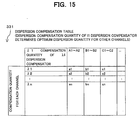
- the memory 33b, as well as the aforesaid reference data memory 22, is for previously storing reference data (frequency data on a reference waveform) to be compared with a received waveform after FFT-processed, and is further for a dispersion compensation table 331 (see FIG. 15) showing the relationship in dispersion compensation quantity among channels.
- the dispersion compensation table 331 is made out on the basis of information (type or the like) of an optical fiber for the optical transmission line 30, or information such as a transmission distance or wavelength spacing.
- information type or the like
- the chromatic dispersion quantity each optical signal with a wavelength ⁇ i undergoes depends upon the type (SMF, DSF or the like) of the optical fiber, transmission distance and wavelength spacing and, hence, if these information are known in advance, when only a chromatic dispersion quantity corresponding to one wave is obtained (actually measured), the chromatic dispersion quantity on another channel is naturally determined therefrom.
- the dispersion compensation table 331 is made to retain, as data in a table format, the relationship between a chromatic dispersion quantity correction value for one wave and chromatic dispersion quantity correction values (or offset values) for other channels, acquired through simulation (or actual measurement) or the like.
- dispersion compensation table 331 data made out previously through the use of a system managing unit such as a maintenance terminal is stored as the dispersion compensation table 331 in the memory 33b, or that the aforesaid information on the optical fiber and information on transmission distance and wavelength spacing are inputted to the processor 33a so that the processor 33a makes out the dispersion compensation table 331 and puts it in the memory 33b.
- the aforesaid processor 33a takes over the processing from the processor 21a on the monitor circuit 8a side and conducts the difference detection (difference calculation; step S13') and dispersion compensation quantity correction value determination (step S14') mentioned above with reference to FIG. 13, and further sees the aforesaid dispersion compensation table 331 on the basis of that correction value to obtain the dispersion compensation quality correction values on other wavelengths (channels) ⁇ 2 to ⁇ n for generating a multi-channel control signal including correction value information on all the wavelengths ⁇ 1 to ⁇ n.
- this function of the processor 33a and the function of the processor 21a is unified to one side.
- control section 33c is for generating, on the basis of the dispersion compensation quantity correction value information on each wavelength ⁇ i included in the multi-channel control signal generated by the processor 33a, a dispersion compensation control signal (CONT1-n; digital signal) for making the variable dispersion compensator 5A-i have a dispersion compensation characteristic corresponding to the correction value.
- Each of the D/A converters 33d-i is for converting the dispersion compensation control signal from this control section 33c into an analog signal, then supplying it to the corresponding variable dispersion compensator 5A-i.
- the processor 21a and the processor 33a take charge of realizing the functions of the aforesaid FFT section 211, difference calculating section 212, compensation characteristic determining section 213 and control signal generating section 214, while the monitor circuit 8a and the processor 33a [calculating means 210 (FFT section 211 and the difference calculating section 212) realize the functions of the aforesaid received signal waveform degradation detecting unit (received waveform degradation detecting means).
- the processor 21a and the multi-channel dispersion compensation control circuit 33 function as an individual compensation control section (control means) to calculate the differences on all the wavelengths ⁇ 1 to ⁇ n on the basis of the difference on a specified wavelength (in this case, wavelength ⁇ 1) for individually controlling the chromatic dispersion compensation characteristic of each variable optical dispersion compensator 5A-i so as to minimize each of the differences.
- this optical recording apparatus 1A as described in the basicmode, with respect to, of the respective wavelengths ⁇ 1 to ⁇ n, only one optical signal with one wave (in this case, ⁇ 1), the equalization amplification output is monitored through the equivalent-time sampling, and the eye pattern of the received signal is recorded (see steps S1 to S9 in FIG. 5), and further the difference relative to the reference waveform is calculated through the FFT calculation to control the dispersion compensation characteristic of the variable dispersion compensator 5A-1 for all the wavelengths ⁇ 1 to ⁇ n on the basis of the calculated difference for individually compensating for the waveform degradation on all the wavelengths ⁇ 1 to ⁇ n (see steps S10 to S12 in FIG. 6 and Steps S13' to S15' in FIG. 13).
- the advantages and effects similar to those of the above-mentioned modification according to the basic mode are obtainable, and in this case, the difference (waveform degradation) detecting system (monitor circuit 8a and dispersion compensation control circuit 33) is required only for one channel, thus realizing and providing a smaller-sized and lower-priced optical receiving apparatus 1A.
- the aforesaid monitor circuit 8a is provided in any one of the optical receiving sections 32-2 to 32-n for the wavelengths ⁇ 2 to ⁇ n other than the wavelength ⁇ 1.
- the monitor circuit 8a is not provided only for one channel, but it is used for each of two or more channels or for each of all the channels.
- the apparatus scale becomes larger, but since the number of channels for the dispersion compensation quantity correction values to be estimated through the use of the dispersion compensation table 331 decreases (that is, it leads to an increase in the number of channels for which correction values are determined on the basis of the actual values) , the compensation accuracy is improvable.
- the reference data memory 22 and the memory for storing the dispersion compensation table 331 are unified as the memory 33b, it is naturally possible that they are designed as separate memories.
- the reference data memory 22 is placed on the monitor circuit 8a side and the processor 21a makes a comparison between a received waveform and a reference waveform.
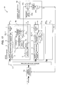
- FIG. 17 is a block diagram showing a configuration of an essential part of an optical receiving apparatus according to a second embodiment of the present invention.
- an optical receiving apparatus 1B is made up of a variable dispersion compensator 5A whose chromatic dispersion characteristic is variable, a WDM coupler (demultiplexer) 31 for demultiplexing a WDM signal from an optical transmission line 30 according to wavelength ⁇ i, a plurality of optical receiving sections 32-1 to 32-n respectively provided with respect to optical signals with the wavelengths ⁇ i after demultiplexed, and a dispersion compensation control circuit 34 for controlling a chromatic dispersion characteristic of the variable dispersion compensator 5A in common with respect to the wavelengths ⁇ i.
- a WDM coupler (demultiplexer) 31 for demultiplexing a WDM signal from an optical transmission line 30 according to wavelength ⁇ i
- a plurality of optical receiving sections 32-1 to 32-n respectively provided with respect to optical signals with the wavelengths ⁇ i after demultiplexed
- the optical receiving section 32-1 for one channel includes an equalization amplified waveform monitor circuit 8b (which will hereinafter be referred to simply as a "monitor circuit 8b") comprising a divider 11, a delay controller 12, a sampler 13, an A/D converter 14, a waveform recording memory 15 and a processor 21b such as a CPU or DSP, and components (a photo-detecting device 2, a preamplifier 3, an equalization amplifier 5, a clock extractor 6 and a decision unit 7) other than the monitor circuit 8b of the optical receiving section 32-1 are provided in each of the remaining optical receiving sections 32-2 to 32-n (in FIG. 17, the internal components of the optical receiving section 32-n are omitted from the illustration).
- an equalization amplified waveform monitor circuit 8b (which will hereinafter be referred to simply as a "monitor circuit 8b") comprising a divider 11, a delay controller 12, a sampler 13, an A/D converter 14, a waveform recording memory 15 and a processor 21b such as a CPU
- the processor 21b takes charge of the reconstruction (step S10) of a received waveform (eye pattern), the FFT arithmetic processing (step S11) and the comparison (step S12) with a reference waveform, mentioned above with reference to FIG. 6. That is, also in this case, in the monitor circuit 8b, the section other than this processor 21b corresponds to the monitor circuit (received waveform measuring means; received signal waveform measuring unit) 8.
- the dispersion compensation control circuit 34 includes a processor 34a, a reference data memory 34b, a control section 34c and a digital/analog (D/A) converter 34d.
- the reference data memory 34b is for storing reference data (frequency data on a reference waveform) to be compared with a received waveform after FFT-processed, and in this case, it is made to record, as reference waveform data, waveform data for the wavelength ⁇ 1 when batch compensation is made for all the channels to accomplish the optimum dispersion compensation.
- the processor 34a takes over the processing from the processor 21b and fulfills the functions to conduct the difference detection (step S13') and the correction value determination on the dispersion compensation quantity of the variable dispersion compensator 5A (step S14') mentioned above with reference to FIG. 13. Also in this case, the function of the processor 34a and the function of the processor 21b can be placed unitarily in one side.
- the control section 34c is for generating a dispersion compensation control signal (digital signal) corresponding to the dispersion compensation quantity correction value obtained in the processor 34a, and the D/A converter 34d converts the dispersion compensation control signal generated in the control section 34c into an analog signal, then supplying it to the variable dispersion compensator 5A.
- the processor 21b and the processor 34a realize the functions of the above-mentioned calculating means 210 (FFT section 211, difference calculating section 212), the compensation characteristic determining section 213 and the control signal generating section 214, while the monitor 8b and the processor 34a [calculating means 210 (FFT section 211 and difference calculating section 212)] realizes the function of the aforesaid received signal waveform degradation detecting unit (received waveform degradation detecting means).
- the processor 21b and the dispersion compensation control circuit 34 function as a batch compensation control section (control means) for batch-controlling the chromatic dispersion characteristic of the variable dispersion compensator 5A in common with respect to the wavelengths ⁇ 1 to ⁇ n.
- the function of the dispersion compensation control circuit 34 it is also possible to incorporate the function of the dispersion compensation control circuit 34 into the monitor circuit 8b and place the incorporated function in the optical receiving section 32-1.
- the equalization amplification output is monitored through the equivalent-time sampling, as described in the basic mode, with respect to, of optical signals having the wavelengths ⁇ 1 to ⁇ n, only an optical signal of one wave (in this case, ⁇ 1) to record an eye pattern of a received signal (see steps S1 to S9 in FIG. 5), and a difference from a reference waveform is obtained through the use of the FFT arithmetic processing to control the dispersion compensation characteristic of the variable dispersion compensator 5A on the basis of the obtained difference for compensating for the waveform degradation on all the wavelengths ⁇ 1 to ⁇ n (see steps S10 to S12 in FIG. 6 and steps S13' to S15' in FIG. 13).
- variable dispersion compensator 5A required is one in number, and the scale of the dispersion compensation control circuit 34 itself is reducible because the D/A converters 34d-i for the respective wavelengths and others become unnecessary, which can realize an optical receiving apparatus 1B reduced in size as a whole and lowered in cost.
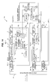
- FIG. 18 is a block diagram showing a configuration of an essential part of an optical receiving apparatus according to a third embodiment of the present invention.
- an optical receiving apparatus 1C is made up of a variable dispersion compensator 5A whose chromatic dispersion characteristic is variable, a WDM coupler (demultiplexer) 31 for demultiplexing a received WDM signal according to wavelength ⁇ i, a plurality of optical receiving sections 32-1 to 32-n respectively provided with respect to the wavelengths ⁇ i after demultiplexed, and a dispersion compensation control circuit 35.
- each of the optical receiving sections 32-1 to 32-n includes a monitor circuit 8 (a divider 11, a delay controller 12, a sampler 13, an A/D converter 14, a waveform recording memory 15 and a processor 21 such as a CPU or DSP) and a control circuit 9 [a processor 21 (an FFT section 211, a difference calculating section 212, a compensation characteristic determining section 213, a control signal generating section 214), a reference data memory 22, a D/A converter 23], shown in FIG. 1, (in FIG. 18, the internal components of the optical receiving section 32-2 are omitted from the illustration).
- a monitor circuit 8 a divider 11, a delay controller 12, a sampler 13, an A/D converter 14, a waveform recording memory 15 and a processor 21 such as a CPU or DSP
- a control circuit 9 [a processor 21 (an FFT section 211, a difference calculating section 212, a compensation characteristic determining section 213, a control signal generating section 214), a reference data memory 22, a D/A
- the dispersion compensation control circuit 35 is composed of a processor 35a such as a CPU or DSP, a control section 35c and a digital/analog (D/A) converter 35d.
- the processor 35a receives information on a difference between a received waveform and a reference waveform, obtained in the processor 21 of each of the control circuits 9 of the optical receiving sections 32-1 and 32-n for two channels (wavelengths ⁇ 1 and ⁇ n), existing at both ends, of the optical receiving sections 32-1 to 32-n for performing a function to obtain the optimum (difference minimizing) dispersion compensation characteristic (correction value) of the variable dispersion compensator 5A on the basis of these information.
- the processor 35a can detect the slope of the chromatic dispersion characteristic additionally. Accordingly, when a device capable of changing not only the chromatic dispersion quantity but also the slope of the chromatic dispersion characteristic is applied to the variable dispersion compensator 5A, it is possible to additionally compensate for the slope of the chromatic dispersion characteristic (called "slope compensation"), thus realizing finer chromatic dispersion compensation.
- slope compensation the slope of the chromatic dispersion characteristic
- the control section 35c is for generating a dispersion compensation control signal (digital signal) corresponding to a correction value of the chromatic dispersion quantity obtained by the processor 35a and the slope of the chromatic dispersion characteristic, while the D/A converter 35d is for converting the dispersion compensation control signal generated by the control section 35c into an analog signal, then supplying it to the variable dispersion compensator 5A.
- the monitor circuit 8 and the processor 21 functioning as the aforesaid received signal waveform degradation detecting unit, are provided for each of all the wavelengths ⁇ 1 to ⁇ n, while the variable dispersion compensator 5A placed at the former stage of the WDM coupler 31 and the frequency characteristic variable type equalization amplifier 5 placed in conjunction with each of electric signals after the photoelectric conversion of demultiplexed optical signals by the WDM coupler 31 made in the photo-detecting device 2 realize a waveform degradation compensating means capable of compensating for the waveform degradation the received WDM signal suffers.
- each of the control circuits 9 performs the function as an equalization amplifier control section to control the frequency characteristic of the corresponding equalization amplifier 5 to minimize the difference between a received waveform and a reference waveform detected by the corresponding waveform degradation detecting unit
- the dispersion compensation control circuit 35 fulfills the function as a batch compensation control section to batch-control the chromatic dispersion characteristic of the variable dispersion compensator 5A in common with respect to the wavelengths ⁇ 1 to ⁇ n on the basis of the differences on the specified wavelengths ⁇ 1 and ⁇ n.
- these control circuits 9 and 35 realize a control means for controlling the compensation characteristics (chromatic dispersion characteristic and frequency characteristic) of the aforesaid variable dispersion compensator 5A and equalization amplifier 5 functioning as the waveform degradation compensating means.
- the function of the dispersion compensation control circuit 35 can be placed unitarily in the function of the control circuit 9 so that the optical receiving section 32-1 or 32-2 has that function additionally.
- the equalization amplification output is monitored through the equivalent-time sampling in the monitor circuit 8 to record the eye pattern of a received signal (see steps S1 to S9 in FIG. 5), and a difference from the frequency data of the reference waveform is obtained through the use of FFT to control the frequency characteristic of the equalization amplifier 5 on the basis of the obtained difference for electrically compensating individually for the waveform degradation of the wavelengths ⁇ 1 to ⁇ n (see steps S10 to S12 in FIG. 6 and steps S13 to S15 in FIG. 7).
- the dispersion compensation control circuit 35 detects a correction value of the dispersion compensation quantity and a slope of the dispersion compensation characteristic so as to minimize the aforesaid difference, and supplies the corresponding dispersion compensation control signal to the variable dispersion compensator 5A, thereby optically conducting the batch dispersion compensation with respect to the optical signals with the wavelengths ⁇ 1 to ⁇ n.
- this optical receiving apparatus 1C is designed to make the compensation at two stages, that is, the variable dispersion compensator 5A performs the optical dispersion compensation in batches with respect to all the channels and the equalization amplifier 5 conducts the electrical dispersion compensation with respect to each of the channels. Therefore, even if the optical batch dispersion compensation cannot achieve the compensation for the waveform degradation, owing to the electrical dispersion compensation according to channel at the latter stage, it is possible to achieve the compensation for received waveform degradation more certainly.
- the electrical dispersion compensation quantity in the equalization amplifier 5 is further reducible as compared with no execution of the optical dispersion compensation. Accordingly, it is possible to lighten the characteristics (compensation capability) such as phase variable width and gain variable width needed for the phase shifter 52, the amplifier 53 and others constituting the equalization amplifier 5, thus realizing this optical receiving apparatus 1C at a lower cost.
- the differences on the both-end wavelengths ⁇ 1 and ⁇ n from the reference waveform are used for obtaining the slope of the chromatic dispersion characteristic in the dispersion compensation control circuit 35, as a matter of course, it is not always necessary to use both end wavelengths, but it is also possible to employ the differences on arbitrary two wavelengths (however, two wavelengths separated as much as possible from each other are more preferable than two wavelengths adjacent to each other). Moreover, naturally, it is also possible to obtain the slope of a chromatic dispersion characteristic through the use of the differences on three or more wavelengths.
- variable dispersion compensator 5A if a device capable of additionally changing the slope of the chromatic dispersion characteristic is applied to the variable dispersion compensator 5A, it is effective to obtain the slope of the chromatic dispersion characteristic using the differences on two or more wavelengths as mentioned above, while in other cases, it is not always necessary to obtain the slope of the chromatic dispersion characteristic.
- a dispersion compensation quantity correction value is acquired on the basis of a difference on one wavelength to control the variable dispersion compensator 5A.
- FIG. 19 is a block diagram showing a configuration of an essential part of an optical receiving apparatus according to a fourth embodiment of the present invention.
- an optical receiving apparatus 1D is made up of an optical dispersion compensator (which will hereinafter be referred to simply as a "dispersion compensator") 5B whose chromatic dispersion characteristic is fixed, a WDM coupler (demultiplexer) 31 for demultiplexing a received WDM signal according to wavelength ⁇ i, and a plurality of optical receiving sections 32-1 to 32-n respectively provided with respect to wavelengths ⁇ i after demultiplexed.
- an optical dispersion compensator which will hereinafter be referred to simply as a "dispersion compensator”
- WDM coupler demultiplexer
- Each of the optical receiving sections 32-i includes a monitor circuit 8 (a divider 11, a delay controller 12, a sampler 13, an A/D converter 14, a waveform recording memory 15 and a processor 21 such as a CPU or DSP) and a control circuit 9 (a processor 21, a reference data memory 22 and a D/A converter 23) shown in FIG. 1 (in FIG. 19, the internal components of the monitor circuit 8 and the optical receiving sections 32-2 to 32-n are omitted from the illustration).
- a monitor circuit 8 a divider 11, a delay controller 12, a sampler 13, an A/D converter 14, a waveform recording memory 15 and a processor 21 such as a CPU or DSP
- a control circuit 9 a processor 21, a reference data memory 22 and a D/A converter 23
- the optical receiving apparatus 1 shown in FIG. 1 is provided a number of wavelengths multiplexed in a WDM signal.
- the monitor circuit 8 and the processor 21 (calculating means 210) functioning as the aforesaid waveform degradation detecting unit, is provided with respect to each of the wavelengths ⁇ i, while the aforesaid dispersion compensator 5B and a plurality of frequency characteristic variable type equalization amplifiers 5 provided with respect to each of the electric signals after the photoelectric conversion of the demultiplexed optical signals by the WDM coupler 31 in the photo-detecting device 2 constitute a waveform degradation compensating means.
- each of the control circuits 9 functions as an equalization amplifier control section for each wavelength ⁇ i to control the frequency characteristic of the corresponding equalization amplifier 5 for minimizing the difference between a received waveform detected by the corresponding waveform degradation detecting unit and a reference waveform, and these control circuits 9 realize a control means for controlling the compensation characteristic of the aforesaid waveform degradation compensating means.
- the dispersion compensator 5B compensates optically for the waveform degradation arising from the chromatic dispersion of a WDM signal to some extent, and each of the optical receiving sections 32-i conducts the monitor/recording of an eye pattern of a received signal, the difference detection from a reference waveform and the frequency characteristic control of the equalization amplifier 5 for minimizing the detected difference, mentioned above in the basic mode, thereby accomplishing the electrical waveform degradation compensation according to wavelength ⁇ i.
- the above-mentioned compensation by the equalization amplifier 5 is similarly feasible with respect to the waveform degradation stemming from the polarization mode dispersion, and when a well-known movable polarization mode dispersion compensator is used in place of the variable dispersion compensator 5A or 5A-i, the compensation at the optical signal stage is also feasible.
- the compensation for the waveform degradation stemming from both the chromatic dispersion and polarization mode dispersion is also feasible through the use of a combination of the variable dispersion compensator 5A (5A-1) and the variable polarization mode dispersion compensator.
- the difference detecting system and the compensation control system are used in common with respect to the chromatic dispersion and the polarization mode dispersion, the size reduction of the apparatus is achievable.
- a section [monitor circuit 8 (8a, 8b)] or a section functioning as a waveform degradation detecting unit functioning as a received signal waveform measuring unit is applicable to any apparatus if it is capable of receiving a signal subjected to waveform degradation, and it is possible to conduct the waveform monitor and detection of the waveform degradation quantity with high accuracy.
- the FFT is used for the conversion of received waveform data into a frequency domain
- the present invention is not limited to this, but it is also possible to employ another method for the conversion into a frequency domain.
Landscapes
- Physics & Mathematics (AREA)
- Electromagnetism (AREA)
- Engineering & Computer Science (AREA)
- Computer Networks & Wireless Communication (AREA)
- Signal Processing (AREA)
- Optical Communication System (AREA)
- Spectrometry And Color Measurement (AREA)
- Photometry And Measurement Of Optical Pulse Characteristics (AREA)
- Cable Transmission Systems, Equalization Of Radio And Reduction Of Echo (AREA)
- Digital Transmission Methods That Use Modulated Carrier Waves (AREA)
- Monitoring And Testing Of Transmission In General (AREA)
Applications Claiming Priority (2)
| Application Number | Priority Date | Filing Date | Title |
|---|---|---|---|
| JP2001059171 | 2001-03-02 | ||
| JP2001059171A JP3798640B2 (ja) | 2001-03-02 | 2001-03-02 | 受信装置及び受信信号の波形劣化補償方法並びに波形劣化検出装置及び方法並びに波形測定装置及び方法 |
Publications (2)
| Publication Number | Publication Date |
|---|---|
| EP1237307A2 true EP1237307A2 (fr) | 2002-09-04 |
| EP1237307A3 EP1237307A3 (fr) | 2006-08-23 |
Family
ID=18918773
Family Applications (1)
| Application Number | Title | Priority Date | Filing Date |
|---|---|---|---|
| EP01120687A Ceased EP1237307A3 (fr) | 2001-03-02 | 2001-09-03 | Récepteur et méthode pour détecter, mesurer et compenser la dégradation de la forme d'onde d'un signal reçu |
Country Status (3)
| Country | Link |
|---|---|
| US (1) | US6694273B2 (fr) |
| EP (1) | EP1237307A3 (fr) |
| JP (1) | JP3798640B2 (fr) |
Cited By (14)
| Publication number | Priority date | Publication date | Assignee | Title |
|---|---|---|---|---|
| WO2004088883A1 (fr) * | 2003-04-03 | 2004-10-14 | Nortel Networks Limited | Compensation de domaine electrique d'effets non lineaires dans un systeme de communications optiques |
| US7023601B2 (en) | 2002-12-02 | 2006-04-04 | Nortel Networks Limited | Optical E-field modulation using a Mach-Zehnder interferometer |
| GB2428169A (en) * | 2005-07-07 | 2007-01-17 | Agilent Technologies Inc | Method and apparatus for providing diagnostic features for an optical transceiver |
| US7200339B1 (en) | 2003-04-11 | 2007-04-03 | Nortel Networks Limited | Method and apparatus for laser line-width compensation |
| WO2007071104A1 (fr) | 2005-12-20 | 2007-06-28 | Zte Corporation | Appareil et procede de compensation de dispersion auto-adaptative |
| US7266306B1 (en) | 2003-10-03 | 2007-09-04 | Nortel Networks Limited | Method for optical carrier suppression and quadrature control |
| US7321734B2 (en) | 2004-07-29 | 2008-01-22 | Nortel Networks Limited | Digital synthesis of readily compensated optical signals |
| US7376358B2 (en) | 2002-10-03 | 2008-05-20 | Nortel Networks Limited | Location specific optical monitoring |
| US7382985B2 (en) | 2002-12-02 | 2008-06-03 | Nortel Networks Limited | Electrical domain mitigation of polarization dependent effects in an optical communications system |
| WO2009152863A1 (fr) | 2008-06-20 | 2009-12-23 | Nokia Siemens Networks Oy | Système de multiplexage de sous-porteuse |
| US7672595B1 (en) | 2003-12-23 | 2010-03-02 | Nortel Networks Limited | Optical transmission system architecture supporting migration to electronic compensation of link impairments |
| US7676161B2 (en) | 2004-12-10 | 2010-03-09 | Nortel Networks Limited | Modulation E-field based control of a non-linear transmitter |
| US7680420B1 (en) | 2003-10-03 | 2010-03-16 | Nortel Networks Limited | Optical E-field modulation using a directly driven laser |
| US7787778B2 (en) | 2004-12-10 | 2010-08-31 | Ciena Corporation | Control system for a polar optical transmitter |
Families Citing this family (66)
| Publication number | Priority date | Publication date | Assignee | Title |
|---|---|---|---|---|
| AU2002324305A1 (en) * | 2001-08-28 | 2003-03-10 | Igor Anatolievich Abrosimov | Adaptive equaliser for reducing distortion in a communication channel |
| JP3856101B2 (ja) * | 2001-09-03 | 2006-12-13 | 日本電気株式会社 | 受信波形整形機能を有する光受信装置 |
| US7116851B2 (en) * | 2001-10-09 | 2006-10-03 | Infinera Corporation | Optical signal receiver, an associated photonic integrated circuit (RxPIC), and method improving performance |
| US7058311B1 (en) * | 2002-03-15 | 2006-06-06 | Xtera Communications, Inc. | System and method for dispersion compensation in an optical communication system |
| US7123788B2 (en) * | 2002-05-06 | 2006-10-17 | Korea Advanced Institute Of Science And Technology | Apparatus for monitoring optical frequencies of WDM signals |
| JP2004032411A (ja) * | 2002-06-26 | 2004-01-29 | Sumitomo Electric Ind Ltd | 光受信器および光通信システム |
| US7668459B2 (en) * | 2002-07-23 | 2010-02-23 | Nippon Telegraph And Telephone Corporation | Dispersion monitoring method and apparatus and dispersion slope temperature dependency compensation method and apparatus |
| JP3990228B2 (ja) | 2002-08-15 | 2007-10-10 | 富士通株式会社 | 光送信装置 |
| JP3880906B2 (ja) | 2002-08-22 | 2007-02-14 | 富士通株式会社 | 波形劣化補償機能を有する受信装置 |
| JP4082992B2 (ja) * | 2002-11-21 | 2008-04-30 | 富士通株式会社 | 光分散モニタ装置および方法、並びに、それを用いた光伝送システム |
| US6990418B2 (en) * | 2002-12-19 | 2006-01-24 | International Business Machines Corporation | Method and systems for optimizing high-speed signal transmission |
| JP2004222240A (ja) * | 2002-12-25 | 2004-08-05 | Nec Corp | 光信号監視方法、及び光信号監視装置 |
| JP3983766B2 (ja) * | 2003-01-10 | 2007-09-26 | 富士通株式会社 | 秘匿性を有する光通信システムおよび光通信方法 |
| WO2004077111A2 (fr) * | 2003-02-27 | 2004-09-10 | Oplink Communications, Inc. | Transpondeur optique adaptatif |
| CA2818683C (fr) | 2003-03-14 | 2015-04-28 | Nippon Telegraph And Telephone Corporation | Dispositif de noeud optique, dispositif de commande de reseau, dispositif associe a du personnel d'entretien, reseau optique et procede de decision associe au noeud de mise en service d'un relais 3r |
| EP1460788B1 (fr) * | 2003-03-20 | 2006-01-25 | Lucent Technologies Inc. | Egaliseur optique à canaux multiples pour la réduction d'interférence intersymbole |
| US20040218701A1 (en) * | 2003-04-29 | 2004-11-04 | Prashant Singh | Protocol agnostic method for adaptive equalization |
| JP4468656B2 (ja) * | 2003-05-27 | 2010-05-26 | 株式会社日立製作所 | 信号波形劣化補償器 |
| US8750725B2 (en) * | 2003-11-18 | 2014-06-10 | Finisar Corporation | Digital optical receiving module, and a method for monitoring the signal quality of a transmitted, modulated optical signal |
| US20050191059A1 (en) * | 2004-01-12 | 2005-09-01 | Clariphy | Use of low-speed components in high-speed optical fiber transceivers |
| JP4091027B2 (ja) | 2004-03-19 | 2008-05-28 | 富士通株式会社 | 光変調器の駆動方法、並びに、それを用いた光送信機および光伝送システム |
| WO2005101703A1 (fr) * | 2004-04-13 | 2005-10-27 | Nec Corporation | Système de surveillance de signal optique |
| US7492816B1 (en) * | 2004-05-25 | 2009-02-17 | Altera Corporation | Adaptive equalization methods and apparatus |
| US7308371B2 (en) * | 2004-06-15 | 2007-12-11 | Intel Corporation | Bit error rate testing for high-speed devices |
| JP4554298B2 (ja) * | 2004-08-20 | 2010-09-29 | 富士通株式会社 | 波長分割多重光伝送システム |
| US20060067699A1 (en) * | 2004-09-24 | 2006-03-30 | Sethumadhavan Chandrasekhar | Equalizer having tunable optical and electronic dispersion compensation |
| JP2006304170A (ja) * | 2005-04-25 | 2006-11-02 | Mitsubishi Electric Corp | Ponシステムおよびponシステムの分散補償方法 |
| US7570889B2 (en) * | 2005-04-28 | 2009-08-04 | Lightwire, Inc. | Common electronic dispersion compensation arrangement for use with multiple optical communication channels |
| JP4820984B2 (ja) * | 2005-06-03 | 2011-11-24 | 国立大学法人 東京大学 | 波形劣化補償方法及び装置 |
| US7606498B1 (en) * | 2005-10-21 | 2009-10-20 | Nortel Networks Limited | Carrier recovery in a coherent optical receiver |
| US7692598B1 (en) | 2005-10-26 | 2010-04-06 | Niitek, Inc. | Method and apparatus for transmitting and receiving time-domain radar signals |
| JP4774103B2 (ja) * | 2006-05-30 | 2011-09-14 | 富士通株式会社 | 分散補償装置 |
| JP4620642B2 (ja) * | 2006-07-31 | 2011-01-26 | 富士通株式会社 | 多値変調受信装置 |
| US7962046B2 (en) * | 2006-11-09 | 2011-06-14 | Newport Corporation | Automated dispersion compensation over a broad wavelength range for coherent optical pulses |
| JP5012811B2 (ja) | 2006-11-30 | 2012-08-29 | 日本電気株式会社 | 分散検出装置およびそれを用いた自動分散補償システム |
| WO2008075548A1 (fr) * | 2006-12-19 | 2008-06-26 | Nec Corporation | Filtre d'égalisation et méthode de compensation de la distorsion |
| JP4303760B2 (ja) | 2007-02-16 | 2009-07-29 | 富士通株式会社 | Ad変換制御装置、光受信装置および光受信方法 |
| IL182937A (en) * | 2007-05-02 | 2011-08-31 | Eci Telecom Ltd | Technique for compensating undesired effects in optical links of an optical communication network |
| US9316729B2 (en) * | 2007-05-25 | 2016-04-19 | Niitek, Inc. | Systems and methods for providing trigger timing |
| US7652619B1 (en) * | 2007-05-25 | 2010-01-26 | Niitek, Inc. | Systems and methods using multiple down-conversion ratios in acquisition windows |
| US7649492B2 (en) * | 2007-05-25 | 2010-01-19 | Niitek, Inc. | Systems and methods for providing delayed signals |
| JP4833157B2 (ja) * | 2007-06-16 | 2011-12-07 | 日本電信電話株式会社 | 光通信装置および光通信システム |
| JP4916387B2 (ja) * | 2007-06-16 | 2012-04-11 | 日本電信電話株式会社 | センタ側光通信装置および光通信システム |
| US7675454B2 (en) * | 2007-09-07 | 2010-03-09 | Niitek, Inc. | System, method, and computer program product providing three-dimensional visualization of ground penetrating radar data |
| US8207885B2 (en) * | 2007-09-19 | 2012-06-26 | Niitek, Inc. | Adjustable pulse width ground penetrating radar |
| US8095005B2 (en) * | 2007-10-26 | 2012-01-10 | Cisco Technology, Inc. | Multimode fiber link probe |
| JP2009117921A (ja) * | 2007-11-01 | 2009-05-28 | Sumitomo Electric Ind Ltd | 光受信器、及び、光受信器の制御方法 |
| WO2009123572A1 (fr) * | 2008-03-31 | 2009-10-08 | Agency For Science, Technology And Research | Noeud distant pour un réseau optique passif multiplexé en longueur d'onde |
| US20100150562A1 (en) * | 2008-12-11 | 2010-06-17 | Electronics And Telecommunications Research Institute | Optical transmission system |
| JP5358486B2 (ja) * | 2010-03-01 | 2013-12-04 | 京セラドキュメントソリューションズ株式会社 | 画像形成装置 |
| WO2011118370A1 (fr) * | 2010-03-26 | 2011-09-29 | 日本電気株式会社 | Dispositif de conversion a/d à procédé à entrelacement dans le temps |
| US9176275B2 (en) | 2010-09-03 | 2015-11-03 | Ofs Fitel, Llc | Dispersion-compensating system and dispersion-compensating fiber with improved figure of merit |
| WO2015000100A1 (fr) * | 2013-07-01 | 2015-01-08 | 华为技术有限公司 | Procédé de compensation de turbo-égalisation, turbo-égaliseur et système |
| JP6131831B2 (ja) | 2013-11-06 | 2017-05-24 | 富士通株式会社 | 光受信器および光受信方法 |
| EP3132548B1 (fr) * | 2014-04-15 | 2021-06-02 | ARRIS Enterprises LLC | Récepteurs et émetteurs intelligents pour réseaux de catv |
| JP6661263B2 (ja) * | 2014-09-03 | 2020-03-11 | 富士通株式会社 | 光伝送装置、非線形歪み補償方法及び非線形歪み予等化方法 |
| US9800348B2 (en) * | 2014-11-18 | 2017-10-24 | Huawei Technologies Co., Ltd. | Chromatic dispersion estimation for digital coherent optical receivers |
| JP6378649B2 (ja) * | 2015-06-29 | 2018-08-22 | 日本電信電話株式会社 | 波長分散推定装置及び光伝送システム |
| US10491299B2 (en) * | 2016-03-15 | 2019-11-26 | Oe Solutions America, Inc. | Electronic dispersion compensation methods and implementations using RLC filter synthesis |
| JP2017175236A (ja) * | 2016-03-18 | 2017-09-28 | 富士通株式会社 | 受信装置、分散補償値制御方法 |
| JP6759742B2 (ja) * | 2016-06-16 | 2020-09-23 | 富士通株式会社 | 受信装置及び設定方法 |
| WO2018053820A1 (fr) * | 2016-09-24 | 2018-03-29 | Huawei Technologies Co., Ltd. | Système et procédé de reconstitution du rythme dans un système de communication optique cohérent |
| JP6376211B2 (ja) * | 2016-11-30 | 2018-08-22 | Nttエレクトロニクス株式会社 | 波長分散補償装置、波長分散補償方法及び通信装置 |
| DE102018107822B3 (de) * | 2018-04-03 | 2019-06-19 | Kathrein Automotive Gmbh | Mobilfunkkompensator zum Einsatz in Kraftfahrzeugen und ein solches Kraftfahrzeug |
| US11962345B2 (en) * | 2022-01-21 | 2024-04-16 | Precision Optical Technologies, Inc. | Configurable dispersion compensation in a pluggable optical transceiver |
| CN115913841B (zh) * | 2022-11-25 | 2024-06-04 | 中北大学 | 一种用于等效时间采样信号的数据均衡方法 |
Family Cites Families (13)
| Publication number | Priority date | Publication date | Assignee | Title |
|---|---|---|---|---|
| JP3010805B2 (ja) | 1991-07-25 | 2000-02-21 | 富士通株式会社 | 受信装置 |
| JPH06268555A (ja) | 1993-03-10 | 1994-09-22 | Oki Electric Ind Co Ltd | 分散等化器 |
| US6307868B1 (en) * | 1995-08-25 | 2001-10-23 | Terayon Communication Systems, Inc. | Apparatus and method for SCDMA digital data transmission using orthogonal codes and a head end modem with no tracking loops |
| DE69735660T2 (de) * | 1996-06-07 | 2006-08-24 | Nortel Networks Ltd. | Faseroptische Übertragungssysteme mit Dispersionsmessung und -kompensation |
| US5935068A (en) * | 1996-11-01 | 1999-08-10 | The Trustees Of The University Of Pennsylvania | System and method for improving ultrasound image contrast by amplitude compression of ultrasonic wavefront signals |
| US6140822A (en) * | 1997-05-29 | 2000-10-31 | Williams; Thomas H. | System for signal path characterization with a reference signal using stepped-frequency increments |
| DE19733764A1 (de) | 1997-08-05 | 1999-02-18 | Alsthom Cge Alcatel | Verfahren und Vorrichtung zum Entzerren eines aufgrund von Störungen im optischen Bereich verzerrten elektrischen Signals |
| JP3649556B2 (ja) * | 1997-08-20 | 2005-05-18 | 富士通株式会社 | 波長分散制御のための方法と装置及び分散量検出方法 |
| JP3476662B2 (ja) * | 1997-10-17 | 2003-12-10 | 富士通株式会社 | ディジタル移動無線通信装置 |
| JPH11122173A (ja) | 1997-10-20 | 1999-04-30 | Fujitsu Ltd | 波長分散による波形変化の検出及びその補償のための方法と装置 |
| EP0954126A1 (fr) * | 1998-04-28 | 1999-11-03 | Lucent Technologies Inc. | Compensation de la dispersion optique |
| CA2400091A1 (fr) * | 2000-02-18 | 2001-08-23 | Corning Incorporated | Detecteur electrique pour commande adaptative de dispersion chromatique dans des systemes optiques |
| JP4671478B2 (ja) * | 2000-08-08 | 2011-04-20 | 富士通株式会社 | 波長多重光通信システムおよび波長多重光通信方法 |
-
2001
- 2001-03-02 JP JP2001059171A patent/JP3798640B2/ja not_active Expired - Fee Related
- 2001-08-22 US US09/933,769 patent/US6694273B2/en not_active Expired - Fee Related
- 2001-09-03 EP EP01120687A patent/EP1237307A3/fr not_active Ceased
Cited By (27)
| Publication number | Priority date | Publication date | Assignee | Title |
|---|---|---|---|---|
| US7382984B2 (en) | 2002-10-03 | 2008-06-03 | Nortel Networks Limited | Electrical domain compensation of optical dispersion in an optical communications system |
| US9853725B2 (en) | 2002-10-03 | 2017-12-26 | Ciena Corporation | Optical dispersion compensation in the electrical domain in an optical communications system |
| US10574352B2 (en) | 2002-10-03 | 2020-02-25 | Ciena Corporation | Compensation of transmitter or receiver defects in an optical communications system |
| US9559778B2 (en) | 2002-10-03 | 2017-01-31 | Ciena Corporation | Optical dispersion compensation in the electrical domain in an optical communications system |
| US10164707B2 (en) | 2002-10-03 | 2018-12-25 | Ciena Corporation | Optical dispersion compensation in the electrical domain in an optical communications system |
| EP1563619B1 (fr) * | 2002-10-03 | 2017-06-07 | Ciena Luxembourg S.a.r.l. | Compensation de la dispersion optique dans le domaine electrique dans un systeme de communication optique |
| EP3211809A1 (fr) * | 2002-10-03 | 2017-08-30 | Ciena Luxembourg S.a.r.l. | Compensation de dispersion optique dans le domaine électrique dans un système de communication optique |
| US7376358B2 (en) | 2002-10-03 | 2008-05-20 | Nortel Networks Limited | Location specific optical monitoring |
| US7756421B2 (en) | 2002-10-03 | 2010-07-13 | Ciena Corporation | Electrical domain compensation of non-linear effects in an optical communications system |
| US7382985B2 (en) | 2002-12-02 | 2008-06-03 | Nortel Networks Limited | Electrical domain mitigation of polarization dependent effects in an optical communications system |
| US7023601B2 (en) | 2002-12-02 | 2006-04-04 | Nortel Networks Limited | Optical E-field modulation using a Mach-Zehnder interferometer |
| WO2004088883A1 (fr) * | 2003-04-03 | 2004-10-14 | Nortel Networks Limited | Compensation de domaine electrique d'effets non lineaires dans un systeme de communications optiques |
| US7200339B1 (en) | 2003-04-11 | 2007-04-03 | Nortel Networks Limited | Method and apparatus for laser line-width compensation |
| US7266306B1 (en) | 2003-10-03 | 2007-09-04 | Nortel Networks Limited | Method for optical carrier suppression and quadrature control |
| US7680420B1 (en) | 2003-10-03 | 2010-03-16 | Nortel Networks Limited | Optical E-field modulation using a directly driven laser |
| US7672595B1 (en) | 2003-12-23 | 2010-03-02 | Nortel Networks Limited | Optical transmission system architecture supporting migration to electronic compensation of link impairments |
| US7321734B2 (en) | 2004-07-29 | 2008-01-22 | Nortel Networks Limited | Digital synthesis of readily compensated optical signals |
| US7787778B2 (en) | 2004-12-10 | 2010-08-31 | Ciena Corporation | Control system for a polar optical transmitter |
| US7676161B2 (en) | 2004-12-10 | 2010-03-09 | Nortel Networks Limited | Modulation E-field based control of a non-linear transmitter |
| GB2428169B (en) * | 2005-07-07 | 2010-05-05 | Agilent Technologies Inc | Method and apparatus for providing diagnostic features for an optical transceiver |
| US7567760B2 (en) | 2005-07-07 | 2009-07-28 | Avago Technologies General Ip (Singapore) Pte. Ltd. | Method and apparatus for providing diagnostic features for an optical transceiver |
| GB2428169A (en) * | 2005-07-07 | 2007-01-17 | Agilent Technologies Inc | Method and apparatus for providing diagnostic features for an optical transceiver |
| EP1971051A4 (fr) * | 2005-12-20 | 2012-08-01 | Zte Corp | Appareil et procede de compensation de dispersion auto-adaptative |
| WO2007071104A1 (fr) | 2005-12-20 | 2007-06-28 | Zte Corporation | Appareil et procede de compensation de dispersion auto-adaptative |
| CN102124676A (zh) * | 2008-06-20 | 2011-07-13 | 诺基亚西门子通信公司 | 子载波复用系统 |
| US8676056B2 (en) | 2008-06-20 | 2014-03-18 | Xieon Networks S.A.R.L. | Subcarrier multiplex system |
| WO2009152863A1 (fr) | 2008-06-20 | 2009-12-23 | Nokia Siemens Networks Oy | Système de multiplexage de sous-porteuse |
Also Published As
| Publication number | Publication date |
|---|---|
| JP2002261692A (ja) | 2002-09-13 |
| JP3798640B2 (ja) | 2006-07-19 |
| US20020123851A1 (en) | 2002-09-05 |
| EP1237307A3 (fr) | 2006-08-23 |
| US6694273B2 (en) | 2004-02-17 |
Similar Documents
| Publication | Publication Date | Title |
|---|---|---|
| US6694273B2 (en) | Receiving apparatus, method of compensating for waveform degradation of received signal, apparatus and method for detecting waveform degradation, and apparatus and method for measuring waveform | |
| EP1392012B1 (fr) | Dispositif de réception avec une fonction de compensation de la dégradation de forme d'onde | |
| US7751706B2 (en) | Chromatic dispersion compensating apparatus | |
| JP4011290B2 (ja) | 分散補償方法、分散補償装置および光伝送システム | |
| CN100539472C (zh) | 信号波形劣化补偿器 | |
| US7489880B2 (en) | Apparatus and method for measuring the dispersion of a fiber span | |
| US8781317B1 (en) | Monitoring phase non-linearities in an optical communication system | |
| US20100239260A1 (en) | Optical transmission apparatus, optical communication method, and optical communication system | |
| EP1614239A1 (fr) | Compensation de domaine electrique d'effets non lineaires dans un systeme de communications optiques | |
| US20090175617A1 (en) | Apparatus and Method for Commissioning an Optical Transmission System | |
| JP2004515186A (ja) | 性能監視方法、光増幅器、光伝送リンク | |
| CN1689255A (zh) | 用于在存在信号失真时测定信号衰减的方法和装置 | |
| JP3960299B2 (ja) | 分散補償方法、wdm光伝送システム、光伝送システム及び光伝送装置 | |
| JP3771755B2 (ja) | 光自動等化器 | |
| JP4175904B2 (ja) | フィルタデバイスの調整方法と装置 | |
| JP3771830B2 (ja) | 自動分散補償回路付き光波長多重伝送システム | |
| JP2001094510A (ja) | 光伝送システム、光伝送路及び光送信装置 | |
| US20040247319A1 (en) | Characterization of a transmission path of an optical signal having an optical communication signal | |
| AU3550700A (en) | Device for channel-specific dispersion compensation of a wavelength multiplex signal | |
| CN1863028B (zh) | 传输光信号的方法和实现该方法的光传输系统 | |
| JP4038656B2 (ja) | 波形歪み検出システム | |
| Zhu et al. | Eight-channel 40 Gb/s RZ transmission over four 80 km spans (328 km) of NDSF with a net dispersion tolerance in excess of 180 ps/nm |
Legal Events
| Date | Code | Title | Description |
|---|---|---|---|
| PUAI | Public reference made under article 153(3) epc to a published international application that has entered the european phase |
Free format text: ORIGINAL CODE: 0009012 |
|
| AK | Designated contracting states |
Kind code of ref document: A2 Designated state(s): AT BE CH CY DE DK ES FI FR GB GR IE IT LI LU MC NL PT SE TR |
|
| AX | Request for extension of the european patent |
Free format text: AL;LT;LV;MK;RO;SI |
|
| PUAL | Search report despatched |
Free format text: ORIGINAL CODE: 0009013 |
|
| AK | Designated contracting states |
Kind code of ref document: A3 Designated state(s): AT BE CH CY DE DK ES FI FR GB GR IE IT LI LU MC NL PT SE TR |
|
| AX | Request for extension of the european patent |
Extension state: AL LT LV MK RO SI |
|
| 17P | Request for examination filed |
Effective date: 20061205 |
|
| AKX | Designation fees paid |
Designated state(s): DE FR GB |
|
| 17Q | First examination report despatched |
Effective date: 20070731 |
|
| STAA | Information on the status of an ep patent application or granted ep patent |
Free format text: STATUS: THE APPLICATION HAS BEEN REFUSED |
|
| 18R | Application refused |
Effective date: 20090406 |