EP1229510B1 - Flüssigkristallanzeigeeinrichtung und Steuerungsverfahren dafür mit Übergang von einem Anfangszustand in einen Anzeigezustand - Google Patents
Flüssigkristallanzeigeeinrichtung und Steuerungsverfahren dafür mit Übergang von einem Anfangszustand in einen Anzeigezustand Download PDFInfo
- Publication number
- EP1229510B1 EP1229510B1 EP02009150A EP02009150A EP1229510B1 EP 1229510 B1 EP1229510 B1 EP 1229510B1 EP 02009150 A EP02009150 A EP 02009150A EP 02009150 A EP02009150 A EP 02009150A EP 1229510 B1 EP1229510 B1 EP 1229510B1
- Authority
- EP
- European Patent Office
- Prior art keywords
- liquid crystal
- transition
- voltage
- alignment
- crystal layer
- Prior art date
- Legal status (The legal status is an assumption and is not a legal conclusion. Google has not performed a legal analysis and makes no representation as to the accuracy of the status listed.)
- Expired - Lifetime
Links
- 239000004973 liquid crystal related substance Substances 0.000 title claims description 236
- 230000007704 transition Effects 0.000 title claims description 176
- 238000000034 method Methods 0.000 title claims description 32
- 239000000758 substrate Substances 0.000 claims description 17
- 239000000463 material Substances 0.000 claims description 16
- 239000011159 matrix material Substances 0.000 claims description 4
- 230000003287 optical effect Effects 0.000 claims description 4
- 230000005236 sound signal Effects 0.000 claims 6
- 238000005401 electroluminescence Methods 0.000 claims 2
- 239000007788 liquid Substances 0.000 claims 1
- 239000007921 spray Substances 0.000 description 11
- 230000001360 synchronised effect Effects 0.000 description 7
- 208000019901 Anxiety disease Diseases 0.000 description 6
- 230000036506 anxiety Effects 0.000 description 6
- 230000007547 defect Effects 0.000 description 6
- 238000010586 diagram Methods 0.000 description 4
- 239000004988 Nematic liquid crystal Substances 0.000 description 3
- 239000005262 ferroelectric liquid crystals (FLCs) Substances 0.000 description 3
- 230000001131 transforming effect Effects 0.000 description 3
- 101100172892 Caenorhabditis elegans sec-8 gene Proteins 0.000 description 2
- 239000004642 Polyimide Substances 0.000 description 2
- 230000003247 decreasing effect Effects 0.000 description 2
- 229920001721 polyimide Polymers 0.000 description 2
- 239000002699 waste material Substances 0.000 description 2
- 101100065878 Caenorhabditis elegans sec-10 gene Proteins 0.000 description 1
- 101100172886 Caenorhabditis elegans sec-6 gene Proteins 0.000 description 1
- 230000005540 biological transmission Effects 0.000 description 1
- 230000004397 blinking Effects 0.000 description 1
- 230000007423 decrease Effects 0.000 description 1
- 230000002950 deficient Effects 0.000 description 1
- 230000001419 dependent effect Effects 0.000 description 1
- 230000008034 disappearance Effects 0.000 description 1
- 230000000694 effects Effects 0.000 description 1
- 230000005611 electricity Effects 0.000 description 1
- 229920005575 poly(amic acid) Polymers 0.000 description 1
- 230000002250 progressing effect Effects 0.000 description 1
- 230000002035 prolonged effect Effects 0.000 description 1
- 230000035939 shock Effects 0.000 description 1
- 125000006850 spacer group Chemical group 0.000 description 1
- 239000000126 substance Substances 0.000 description 1
Images


Classifications
-
- G—PHYSICS
- G09—EDUCATION; CRYPTOGRAPHY; DISPLAY; ADVERTISING; SEALS
- G09G—ARRANGEMENTS OR CIRCUITS FOR CONTROL OF INDICATING DEVICES USING STATIC MEANS TO PRESENT VARIABLE INFORMATION
- G09G3/00—Control arrangements or circuits, of interest only in connection with visual indicators other than cathode-ray tubes
- G09G3/20—Control arrangements or circuits, of interest only in connection with visual indicators other than cathode-ray tubes for presentation of an assembly of a number of characters, e.g. a page, by composing the assembly by combination of individual elements arranged in a matrix no fixed position being assigned to or needed to be assigned to the individual characters or partial characters
- G09G3/34—Control arrangements or circuits, of interest only in connection with visual indicators other than cathode-ray tubes for presentation of an assembly of a number of characters, e.g. a page, by composing the assembly by combination of individual elements arranged in a matrix no fixed position being assigned to or needed to be assigned to the individual characters or partial characters by control of light from an independent source
- G09G3/36—Control arrangements or circuits, of interest only in connection with visual indicators other than cathode-ray tubes for presentation of an assembly of a number of characters, e.g. a page, by composing the assembly by combination of individual elements arranged in a matrix no fixed position being assigned to or needed to be assigned to the individual characters or partial characters by control of light from an independent source using liquid crystals
- G09G3/3611—Control of matrices with row and column drivers
-
- G—PHYSICS
- G02—OPTICS
- G02F—OPTICAL DEVICES OR ARRANGEMENTS FOR THE CONTROL OF LIGHT BY MODIFICATION OF THE OPTICAL PROPERTIES OF THE MEDIA OF THE ELEMENTS INVOLVED THEREIN; NON-LINEAR OPTICS; FREQUENCY-CHANGING OF LIGHT; OPTICAL LOGIC ELEMENTS; OPTICAL ANALOGUE/DIGITAL CONVERTERS
- G02F1/00—Devices or arrangements for the control of the intensity, colour, phase, polarisation or direction of light arriving from an independent light source, e.g. switching, gating or modulating; Non-linear optics
- G02F1/01—Devices or arrangements for the control of the intensity, colour, phase, polarisation or direction of light arriving from an independent light source, e.g. switching, gating or modulating; Non-linear optics for the control of the intensity, phase, polarisation or colour
- G02F1/13—Devices or arrangements for the control of the intensity, colour, phase, polarisation or direction of light arriving from an independent light source, e.g. switching, gating or modulating; Non-linear optics for the control of the intensity, phase, polarisation or colour based on liquid crystals, e.g. single liquid crystal display cells
- G02F1/133—Constructional arrangements; Operation of liquid crystal cells; Circuit arrangements
- G02F1/1333—Constructional arrangements; Manufacturing methods
- G02F1/1343—Electrodes
- G02F1/134309—Electrodes characterised by their geometrical arrangement
- G02F1/134336—Matrix
-
- G—PHYSICS
- G02—OPTICS
- G02F—OPTICAL DEVICES OR ARRANGEMENTS FOR THE CONTROL OF LIGHT BY MODIFICATION OF THE OPTICAL PROPERTIES OF THE MEDIA OF THE ELEMENTS INVOLVED THEREIN; NON-LINEAR OPTICS; FREQUENCY-CHANGING OF LIGHT; OPTICAL LOGIC ELEMENTS; OPTICAL ANALOGUE/DIGITAL CONVERTERS
- G02F1/00—Devices or arrangements for the control of the intensity, colour, phase, polarisation or direction of light arriving from an independent light source, e.g. switching, gating or modulating; Non-linear optics
- G02F1/01—Devices or arrangements for the control of the intensity, colour, phase, polarisation or direction of light arriving from an independent light source, e.g. switching, gating or modulating; Non-linear optics for the control of the intensity, phase, polarisation or colour
- G02F1/13—Devices or arrangements for the control of the intensity, colour, phase, polarisation or direction of light arriving from an independent light source, e.g. switching, gating or modulating; Non-linear optics for the control of the intensity, phase, polarisation or colour based on liquid crystals, e.g. single liquid crystal display cells
- G02F1/137—Devices or arrangements for the control of the intensity, colour, phase, polarisation or direction of light arriving from an independent light source, e.g. switching, gating or modulating; Non-linear optics for the control of the intensity, phase, polarisation or colour based on liquid crystals, e.g. single liquid crystal display cells characterised by the electro-optical or magneto-optical effect, e.g. field-induced phase transition, orientation effect, guest-host interaction or dynamic scattering
- G02F1/139—Devices or arrangements for the control of the intensity, colour, phase, polarisation or direction of light arriving from an independent light source, e.g. switching, gating or modulating; Non-linear optics for the control of the intensity, phase, polarisation or colour based on liquid crystals, e.g. single liquid crystal display cells characterised by the electro-optical or magneto-optical effect, e.g. field-induced phase transition, orientation effect, guest-host interaction or dynamic scattering based on orientation effects in which the liquid crystal remains transparent
- G02F1/1393—Devices or arrangements for the control of the intensity, colour, phase, polarisation or direction of light arriving from an independent light source, e.g. switching, gating or modulating; Non-linear optics for the control of the intensity, phase, polarisation or colour based on liquid crystals, e.g. single liquid crystal display cells characterised by the electro-optical or magneto-optical effect, e.g. field-induced phase transition, orientation effect, guest-host interaction or dynamic scattering based on orientation effects in which the liquid crystal remains transparent the birefringence of the liquid crystal being electrically controlled, e.g. ECB-, DAP-, HAN-, PI-LC cells
- G02F1/1395—Optically compensated birefringence [OCB]- cells or PI- cells
-
- G—PHYSICS
- G09—EDUCATION; CRYPTOGRAPHY; DISPLAY; ADVERTISING; SEALS
- G09G—ARRANGEMENTS OR CIRCUITS FOR CONTROL OF INDICATING DEVICES USING STATIC MEANS TO PRESENT VARIABLE INFORMATION
- G09G3/00—Control arrangements or circuits, of interest only in connection with visual indicators other than cathode-ray tubes
- G09G3/20—Control arrangements or circuits, of interest only in connection with visual indicators other than cathode-ray tubes for presentation of an assembly of a number of characters, e.g. a page, by composing the assembly by combination of individual elements arranged in a matrix no fixed position being assigned to or needed to be assigned to the individual characters or partial characters
- G09G3/34—Control arrangements or circuits, of interest only in connection with visual indicators other than cathode-ray tubes for presentation of an assembly of a number of characters, e.g. a page, by composing the assembly by combination of individual elements arranged in a matrix no fixed position being assigned to or needed to be assigned to the individual characters or partial characters by control of light from an independent source
- G09G3/3406—Control of illumination source
-
- G—PHYSICS
- G09—EDUCATION; CRYPTOGRAPHY; DISPLAY; ADVERTISING; SEALS
- G09G—ARRANGEMENTS OR CIRCUITS FOR CONTROL OF INDICATING DEVICES USING STATIC MEANS TO PRESENT VARIABLE INFORMATION
- G09G3/00—Control arrangements or circuits, of interest only in connection with visual indicators other than cathode-ray tubes
- G09G3/20—Control arrangements or circuits, of interest only in connection with visual indicators other than cathode-ray tubes for presentation of an assembly of a number of characters, e.g. a page, by composing the assembly by combination of individual elements arranged in a matrix no fixed position being assigned to or needed to be assigned to the individual characters or partial characters
- G09G3/34—Control arrangements or circuits, of interest only in connection with visual indicators other than cathode-ray tubes for presentation of an assembly of a number of characters, e.g. a page, by composing the assembly by combination of individual elements arranged in a matrix no fixed position being assigned to or needed to be assigned to the individual characters or partial characters by control of light from an independent source
- G09G3/36—Control arrangements or circuits, of interest only in connection with visual indicators other than cathode-ray tubes for presentation of an assembly of a number of characters, e.g. a page, by composing the assembly by combination of individual elements arranged in a matrix no fixed position being assigned to or needed to be assigned to the individual characters or partial characters by control of light from an independent source using liquid crystals
- G09G3/3611—Control of matrices with row and column drivers
- G09G3/3648—Control of matrices with row and column drivers using an active matrix
-
- G—PHYSICS
- G09—EDUCATION; CRYPTOGRAPHY; DISPLAY; ADVERTISING; SEALS
- G09G—ARRANGEMENTS OR CIRCUITS FOR CONTROL OF INDICATING DEVICES USING STATIC MEANS TO PRESENT VARIABLE INFORMATION
- G09G2300/00—Aspects of the constitution of display devices
- G09G2300/04—Structural and physical details of display devices
- G09G2300/0469—Details of the physics of pixel operation
- G09G2300/0478—Details of the physics of pixel operation related to liquid crystal pixels
- G09G2300/0491—Use of a bi-refringent liquid crystal, optically controlled bi-refringence [OCB] with bend and splay states, or electrically controlled bi-refringence [ECB] for controlling the color
-
- G—PHYSICS
- G09—EDUCATION; CRYPTOGRAPHY; DISPLAY; ADVERTISING; SEALS
- G09G—ARRANGEMENTS OR CIRCUITS FOR CONTROL OF INDICATING DEVICES USING STATIC MEANS TO PRESENT VARIABLE INFORMATION
- G09G2310/00—Command of the display device
- G09G2310/02—Addressing, scanning or driving the display screen or processing steps related thereto
- G09G2310/024—Scrolling of light from the illumination source over the display in combination with the scanning of the display screen
-
- G—PHYSICS
- G09—EDUCATION; CRYPTOGRAPHY; DISPLAY; ADVERTISING; SEALS
- G09G—ARRANGEMENTS OR CIRCUITS FOR CONTROL OF INDICATING DEVICES USING STATIC MEANS TO PRESENT VARIABLE INFORMATION
- G09G2310/00—Command of the display device
- G09G2310/06—Details of flat display driving waveforms
-
- G—PHYSICS
- G09—EDUCATION; CRYPTOGRAPHY; DISPLAY; ADVERTISING; SEALS
- G09G—ARRANGEMENTS OR CIRCUITS FOR CONTROL OF INDICATING DEVICES USING STATIC MEANS TO PRESENT VARIABLE INFORMATION
- G09G2310/00—Command of the display device
- G09G2310/06—Details of flat display driving waveforms
- G09G2310/061—Details of flat display driving waveforms for resetting or blanking
- G09G2310/063—Waveforms for resetting the whole screen at once
-
- G—PHYSICS
- G09—EDUCATION; CRYPTOGRAPHY; DISPLAY; ADVERTISING; SEALS
- G09G—ARRANGEMENTS OR CIRCUITS FOR CONTROL OF INDICATING DEVICES USING STATIC MEANS TO PRESENT VARIABLE INFORMATION
- G09G2310/00—Command of the display device
- G09G2310/06—Details of flat display driving waveforms
- G09G2310/065—Waveforms comprising zero voltage phase or pause
-
- G—PHYSICS
- G09—EDUCATION; CRYPTOGRAPHY; DISPLAY; ADVERTISING; SEALS
- G09G—ARRANGEMENTS OR CIRCUITS FOR CONTROL OF INDICATING DEVICES USING STATIC MEANS TO PRESENT VARIABLE INFORMATION
- G09G2310/00—Command of the display device
- G09G2310/08—Details of timing specific for flat panels, other than clock recovery
-
- G—PHYSICS
- G09—EDUCATION; CRYPTOGRAPHY; DISPLAY; ADVERTISING; SEALS
- G09G—ARRANGEMENTS OR CIRCUITS FOR CONTROL OF INDICATING DEVICES USING STATIC MEANS TO PRESENT VARIABLE INFORMATION
- G09G2320/00—Control of display operating conditions
- G09G2320/04—Maintaining the quality of display appearance
- G09G2320/041—Temperature compensation
-
- G—PHYSICS
- G09—EDUCATION; CRYPTOGRAPHY; DISPLAY; ADVERTISING; SEALS
- G09G—ARRANGEMENTS OR CIRCUITS FOR CONTROL OF INDICATING DEVICES USING STATIC MEANS TO PRESENT VARIABLE INFORMATION
- G09G2330/00—Aspects of power supply; Aspects of display protection and defect management
- G09G2330/02—Details of power systems and of start or stop of display operation
- G09G2330/021—Power management, e.g. power saving
- G09G2330/022—Power management, e.g. power saving in absence of operation, e.g. no data being entered during a predetermined time
-
- G—PHYSICS
- G09—EDUCATION; CRYPTOGRAPHY; DISPLAY; ADVERTISING; SEALS
- G09G—ARRANGEMENTS OR CIRCUITS FOR CONTROL OF INDICATING DEVICES USING STATIC MEANS TO PRESENT VARIABLE INFORMATION
- G09G2330/00—Aspects of power supply; Aspects of display protection and defect management
- G09G2330/02—Details of power systems and of start or stop of display operation
- G09G2330/026—Arrangements or methods related to booting a display
-
- G—PHYSICS
- G09—EDUCATION; CRYPTOGRAPHY; DISPLAY; ADVERTISING; SEALS
- G09G—ARRANGEMENTS OR CIRCUITS FOR CONTROL OF INDICATING DEVICES USING STATIC MEANS TO PRESENT VARIABLE INFORMATION
- G09G3/00—Control arrangements or circuits, of interest only in connection with visual indicators other than cathode-ray tubes
- G09G3/20—Control arrangements or circuits, of interest only in connection with visual indicators other than cathode-ray tubes for presentation of an assembly of a number of characters, e.g. a page, by composing the assembly by combination of individual elements arranged in a matrix no fixed position being assigned to or needed to be assigned to the individual characters or partial characters
- G09G3/34—Control arrangements or circuits, of interest only in connection with visual indicators other than cathode-ray tubes for presentation of an assembly of a number of characters, e.g. a page, by composing the assembly by combination of individual elements arranged in a matrix no fixed position being assigned to or needed to be assigned to the individual characters or partial characters by control of light from an independent source
- G09G3/36—Control arrangements or circuits, of interest only in connection with visual indicators other than cathode-ray tubes for presentation of an assembly of a number of characters, e.g. a page, by composing the assembly by combination of individual elements arranged in a matrix no fixed position being assigned to or needed to be assigned to the individual characters or partial characters by control of light from an independent source using liquid crystals
- G09G3/3611—Control of matrices with row and column drivers
- G09G3/3648—Control of matrices with row and column drivers using an active matrix
- G09G3/3651—Control of matrices with row and column drivers using an active matrix using multistable liquid crystals, e.g. ferroelectric liquid crystals
Definitions
- the present invention relates to liquid crystal display apparatuses which require a transition of liquid crystal molecules in a liquid crystal layer from an initial alignment to a predetermined displayable alignment in advance of displaying. More particularly, this invention relates to an improvement in methods of driving such apparatuses with the transition of the alignment of liquid crystal molecules.
- Widely used twisted nematic mode liquid crystal display apparatuses which employ nematic liquid crystals have shortcomings such as a slow response and a narrow viewing angle.
- Ferroelectric liquid crystal mode liquid crystal display apparatuses exhibit a quick response and have a wide viewing angle, but also have great shortcomings in shock resistance, temperature property and the like.
- optically compensated bend mode (or optically compensated birefringence mode) liquid crystal display apparatuses (hereinafter, referred to as "OCB mode liquid crystal display apparatuses"), which were proposed in Japanese Unexamined Patent Publications No. Hei 7-84254 or Shingaku Technical Reports (ED198-144, on page 19, published by the Corporation of Electricity Communication Institute) exhibit a quick response and have a wide viewing angle. The apparatuses, therefore, will be expected to be applied to liquid crystal televisions and the like as transmission or reflection type liquid crystal display apparatuses hereafter.
- EP 854 465 relates to another known driving method for liquid crystal displays with a bend alignment.
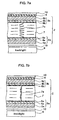
- FIG. 7a shows an example of OCB mode liquid crystal display apparatuses.
- a liquid crystal panel 2 includes an array substrate 3a with transparent pixel electrodes 4a provided thereon, a counter substrate 3b with transparent counter electrodes 4b provided thereon and a liquid crystal layer 7 sandwiched between the array substrate 3a and the counter substrate 3b.
- Liquid crystal alignment layers 6a and 6b of polyimide are formed on internal surfaces of the array substrate 3a and the counter substrate 3b, on which the pixel electrodes 4a and the counter electrodes 4b are provided, respectively. Both the liquid crystal alignment layers 6a and 6b had been treated with rubbing, and the substrates 3a and 3b are disposed so that the rubbing directions of the liquid crystal alignment layers 6a and 6b are parallel to each other.
- the liquid crystal layer 7 is filled with a nematic liquid crystal material having a positive dielectric anisotropy.
- pretilt angles of liquid crystal molecules 7a on both of the array substrate 3a and the counter substrate 3b are approximately several to 10 degrees in reverse directions.
- the liquid crystal molecules 7a offers an alignment such as to be inclined symmetrically and outwardly on a plane or a splay alignment.
- a voltage pulse for transition a voltage pulse with a comparatively high voltage between the pixel electrode 4a and the counter electrode 4b in a short time when a main power is switched on
- the liquid crystal molecules 7a having a spray alignment as shown in Fig. 7a locally rise and a micro area of bend alignment or bend alignment including twisted alignment (hereinafter, referred to as "a transition core") is generated as shown in Fig. 7b .
- the transition core is spread by repeatedly applying the voltage pulse for transition.
- the transition of the whole liquid crystal material in the liquid crystal layer 7 to bend alignment enables an OCB mode liquid crystal display apparatus to display.
- An OCB mode liquid crystal display apparatus can display by utilizing a change in retardation resulting from a change in bend alignment of the liquid crystal molecule 7a, which is caused by applying display signal driving voltage.
- phase-compensation plate 8 for optically compensating in order to enable a low voltage driving of the liquid crystal panel 2 as well as widen a viewing angle, with an optical axis thereof being fixed in a predetermined direction.
- An FLC type liquid crystal display apparatus and a phase transition type liquid crystal display apparatus involve similar requirements before being shifted to an ordinary display-driving mode.
- a fine display can not be obtained when shifted to a display-driving mode.
- an OCB mode liquid crystal display apparatus when the transition to bend alignment is not completed and an area of splay alignment remains locally, the remaining area becomes a bright point in display driving and looks like a point defect. The image is displayed dimly and unstably for several seconds to several minutes after starting display driving. Consequently, the transition to bend alignment must be certainly completed before being shifted to the display-driving mode.
- the transition core is accidentally generated or not generated in the same place even if the voltage pulse for transition is applied on the same conditions, leading to the difficulty in certainly completing the transition in a short time.
- a backlight is turned on when a main power of the apparatus is switched on.
- an output of voice from a speaker starts simultaneously.
- liquid crystal display apparatuses for carrying out the transition of the alignment of liquid crystal molecules in the liquid crystal layer to a predetermined alignment in advance of displaying it occasionally takes a long time to be shifted to the ordinary display-driving mode. It is a waste of energy to switch on the backlight for the shift period to the display-driving mode or the transition period.
- the display having many point alignment defects and plane alignment defects due to pixels with no transition or under transition as well as the blinking of the whole screen due to the application of the voltage pulse for transition are the causes of users' discomfort and anxiety. Disappearance of the above-mentioned defects due to alignment transition can delete such sense of incongruity thereby realizing liquid crystal display apparatuses which can display images with high quality and are excellent in commercial view
- the object of the present invention is to solve the above-mentioned problems thereby to provide methods of driving liquid crystal display apparatuses of which an initial alignment of liquid crystal molecules is different from the displayable alignment such as an OCB mode liquid crystal display apparatus, enabling a certainly completion of a transition of the liquid crystal molecules to the displayable alignment in a short time and avoiding the display of unwanted images.
- a method for driving a liquid crystal display apparatus in the present invention is a method for driving a liquid crystal display as set out in claim 1, and an apparatus for driving such a liquid crystal display as set out in claim 18.
- Preferrable implementations are set out in the attached dependent claims.
- OCB mode liquid crystal display apparatuses are described as examples in the following embodiments.
- a method for certainly carrying out a transition of a liquid crystal layer from an initial alignment to a displayable alignment, in advance of displaying a panel is detailed referring to the drawings in the present example, not forming part of the invention.
- a pair of substrates 3a and 3b are basically disposed so that rubbing directions of the liquid crystal alignment layers 6a and 6b formed on surfaces contacting the liquid crystal layer 7 are parallel to each other.
- the liquid crystal molecules 7a in the liquid crystal layer 7 are arrayed approximately in parallel, namely, spray alignment as shown in Fig. 7a .
- the transition from the spray alignment to bend alignment as shown in Fig. 7b is required for displaying a panel.
- transition cores An application of the voltage pulse for transition locally generates micro areas of bend alignment (hereinafter, referred to as "transition cores"), thereafter the transition core is gradually growing. If the transition core generates in a pixel, the transition to bend alignment is started therefrom.
- a forming portion of the transition core is provided in auxiliary capacity provided near a gate line in a pixel. It is possible to generate the transition core in a desirable place by providing a projection at an electrode or by providing on a liquid crystal alignment layer an area such that a pretilt angle of a liquid crystal molecule thereon is different from that of a liquid crystal molecule on another area, for example.
- Rubbing Direction 415 750 910 1,320 1,636 2,829 3,039 4,000 Vertical Direction 162 427 585 720 1,034 1,618 1,798 2,247 0°C Rubbing Direction 145 236 327 400 591 727 818 955 Vertical Direction 87 140 191 243 348 435 478 522 -10°C Rubbing Direction 64 109 164 164 236 318 333 500 Vertical Direction 35 61 87 96 130 163 202 240 ( ⁇ m/sec)
- the growth rate of the transformed area of bend alignment depends on each of temperature and applied voltage.
- the growth rate in the rubbing direction of the liquid crystal alignment layer is faster than that in a vertical direction to the rubbing direction. Accordingly, the area of bend alignment can be formed in a short time by equalizing a longitudinal direction of a rectangular pixel to the rubbing direction.
- the voltage application time of 0.04 sec and 0.12 sec were sufficient for a liquid crystal panel having a pixel area of 160 ⁇ m ⁇ 50 ⁇ m and having that of 450 ⁇ m ⁇ 150 ⁇ m, respectively, at a room temperature of 25°C where a growth rate is 4,000 ⁇ m /sec.
- the growth rate varies with temperature as described above. If the application time of the voltage pulse for transition to bend alignment is excessive, a normal display can not be performed for the excessive time resulting in a waste of time to users. On the other hand, if the transition to bend alignment is insufficient, a normal display can not occasionally be performed.
- a temperature sensor therefore, is installed in a liquid crystal panel so that the time for applying voltage is determined on the basis of the measured panel temperature. This method makes it possible to set as much time as is necessary for the transition and to prevent excess and insufficiency in the transition.
- the voltage application time of 0.16 second or more was sufficient for a liquid crystal panel having a pixel area of 160 ⁇ m ⁇ 50 ⁇ m, and that of 0.45 second or more was sufficient for a pixel area of 450 ⁇ m ⁇ 150 ⁇ m at the lowest temperature for assuring the operations (0°C) where a growth rate is 1,000 ⁇ m /sec.
- the voltage pulse for transition is applied intermittently or continuously.
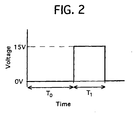
- the sum of the application time corresponds to T 1 shown in Fig. 2 in the case of applying intermittently.
- a pause period To representing the applied voltage of 0 V was set before the voltage application time represented by T 1 in Fig. 2 .
- the pause period To enables the transition core to be generated stably and the transition to be progressed stably.
- the transition can be progressed more stably with the longer pause period
- the pause period of approximately 0.2 second enables a stable transition.
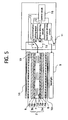
- Fig. 3 shows a schematic constitution of a liquid crystal display apparatus in this embodiment.
- the liquid crystal display apparatus is an OCB mode liquid crystal display apparatus.
- a liquid crystal display apparatus 1 includes a 7-inch model active matrix type liquid crystal panel 2, a pair of film-shaped retardation plates 8 for optically compensating in order to enable a low voltage driving as well as widen a viewing angle, a pair of polarizers 10 and a backlight 9 for projecting lights to the liquid crystal panel 2.
- the liquid crystal panel 2 has the same structure as that shown in Fig. 7a .
- a control unit 11 includes a display-driving circuit 12 for outputting a driving signal for displaying in display driving, a transition-driving circuit 13 for outputting a voltage pulse for performing the transition of a liquid crystal layer to bend alignment, a backlight-driving circuit 14 for ON/OFF-controlling the backlight 9 and a control circuit 16 for controlling these circuits.
- the transition-driving circuit 13 intermittently applies a voltage pulse with a high voltage such as 15 V for performing a liquid crystal layer 7 from spray alignment to bend alignment between the pixel electrode 4a and the counter electrode 4b of the same liquid crystal panel 2 as shown in Fig. 7a for a certain time.
- a voltage pulse with a high voltage such as 15 V for performing a liquid crystal layer 7 from spray alignment to bend alignment between the pixel electrode 4a and the counter electrode 4b of the same liquid crystal panel 2 as shown in Fig. 7a for a certain time.
- This liquid crystal display apparatus requires 2 seconds of the voltage pulse application in order to transform the liquid crystal layer 7 in all pixels of the liquid crystal panel 2 from spray alignment to bend alignment at room temperature.
- the control circuit 16 When a main power of the liquid crystal display apparatus 1 is switched on, the control circuit 16 connects a switch 15 to a terminal "A" and the transition-driving circuit 13 applies the high voltage pulse for transition to the liquid crystal panel 2 for 2 seconds.
- the application of the voltage pulse for transition can carry out a transition of the liquid crystal molecule 7a in the liquid crystal layer 7 from spray alignment to bend alignment.
- the control circuit 16 When the application of the voltage pulse for transition is finished, the control circuit 16 connects the switch 15 to a terminal "B" and connects the display-driving circuit 12 with the liquid crystal panel 2.
- the control circuit 16 is synchronized with the connection between the display-driving circuit 12 and the liquid crystal panel 2 to operate the backlight-driving circuit 14 and switch on the backlight 9.
- the liquid crystal display apparatus 1 is shifted to a display-driving mode.
- the liquid crystal display apparatus 1 in this embodiment does not offer a defective display such that the screen blinks intermittently, and point defect and plane defect appear on the whole surface of a liquid crystal panel during the transition as in conventional liquid crystal display in which the voltage pulse for transition is applied after switching on a backlight. Consequently, users' discomfort and anxiety about troubles can be prevented from being caused.
- An OCB mode liquid crystal display apparatus in which the display is performed after carrying out the transition of the liquid crystal molecules in a liquid crystal layer from spray alignment to bend alignment is described in the present embodiment, as one example.
- the transition can be induced by providing a projection at an electrode or providing on a liquid crystal alignment layer a specific area such that a pretilt angle of a liquid crystal molecule thereon is different from that of a liquid crystal molecule on another area, resulting in the completion of transforming within a predetermined time.
- a higher voltage such as approximately 25 V
- driving-signals for displaying is applied between electrodes as the voltage pulse for the transition.
- the application of so high voltage requires great power consumption in transforming.
- a voltage value of the voltage pulse for transition is approximately equal to the driving-signal for displaying of 5 to 6 V
- the liquid crystal molecules in the liquid crystal layer were transformed from spray alignment to bend alignment under the low voltage despite approximately 30 seconds. That is, an electric power supply system for the transition does not always have to be provided separately from the system for displaying. Accordingly, the equalization of a voltage signal of the voltage pulse for transition to that of the driving signal for displaying decreases the power consumption and reduces the costs of the apparatus.
- control circuit 16 can also connect the liquid crystal panel 2 with the transition-driving circuit 13 or the display-driving circuit 12, being synchronized with the open and close of the cover 17.
- the control circuit 16 judges whether to apply the voltage pulse for transition to the liquid crystal panel 2 or not.
- control circuit 16 determines to apply the voltage pulse for transition, the control circuit 16 operates the switch 15 to connect the liquid crystal panel 2 with the transition-driving circuit 13 and the voltage pulse for transition is applied to the liquid crystal panel 2 for 1 second, for example. After applying the voltage pulse for transition, the control circuit 16 operates the switch 15 to connect the liquid crystal panel 2 with the display-driving circuit 12 and the backlight 9 is turned on, being synchronized with the connection. As a result, the apparatus is shifted to an ordinary display-driving mode.
- control circuit 16 judges not to apply the voltage pulse for transition, the control circuit 16 operates the switch 15 to connect the liquid crystal panel 2 with the display-driving circuit 12 and the backlight 9 is turned on, being synchronized with the connection. As a result, the apparatus is shifted to an ordinary display-driving mode.
- control circuit 16 When the cover 17 is closed with the main power on, the control circuit 16 operates the switch 15 to connect the liquid crystal panel 2 with the transition-driving circuit 13 and thereafter apply the voltage pulse for transition to the liquid crystal panel 2 in order to maintain the bend alignment. In addition, the control circuit 16 switches off the backlight 9, being synchronized with the application.
- control circuit 16 When an input from the user is not recognized for a predetermined time, the control circuit 16 similarly operates the switch 15 to connect the liquid crystal panel 2 with the transition-driving circuit 13 and the voltage pulse for transition is applied to the liquid crystal panel 2 in order to maintain the bend alignment. In addition, the control circuit 16 switches off the backlight 9, being synchronized with the application.
- control circuit 16 When an input from the user is recognized, the control circuit 16 operates the switch 15 to connect the liquid crystal panel 2 with the display-driving circuit 12 and thereafter switch on the backlight 9, being synchronized with the connection. As a result, the apparatus is shifted to an ordinary display-driving mode.
- control circuit 16 These operations of the control circuit 16 are useful for the driving of a notebook type personal computer, a mobile computer, a folding portable phone and the like.
- liquid crystal display apparatuses having a speaker such as liquid crystal televisions
- the speaker is employed as a means of notifying the progress or completion of the transition.
- the voltage pulse for transition is applied for a predetermined time (2 seconds, for example).
- aural signal for notifying the progress of the transition is output from the speaker during the transition driving. That is, since the aural signal is output from the speaker before the transition is completed and the backlight is switched on, the user can be relieved during the transition-driving to recognize that the apparatus is starting up.
- an output of a voice for broadcasting from a speaker is started at the moment with a main power switched on, and a voice signal for notifying a progressional state of the transition is superposed on a voice signal for broadcasting.
- the time lag from switching on to the start of image display and voice output can be a cause of users' anxiety. It, therefore, is desirable to prevent such users' anxiety by starting voice output previous to image display after switching on.
- the transition driving is completed, the backlight is switched on and the apparatus is shifted to a display-driving mode, then the aural signal for notifying the completion of the transition is output from the speaker. Needless to say, the aural signal may be output after switching on the backlight.
- a small-sized lamp, a light-emitting diode, an EL element and the like may be switched on as a sign for notifying the progress or completion of the transition to the user until the backlight is switched on, and after the transition is completed, the backlight may be switched on.
- the user can be relieved from anxiety about troubles.
- the transition-driving circuit instead of predetermining the time for completing the transition in the transition-driving circuit, there may be provided a means of visually observing the liquid crystal panel and judging the completion of the transition to bend alignment although the constitution becomes complicated.
- the backlight is switched on after the transition driving is completed. Furthermore, the backlight does not always have to be switched on immediately after the transition-driving is completed, and the backlight may be switched on only while the liquid crystal panel is in the display-driving mode.
- a transmission-type liquid crystal display apparatus is described in the present invention.
- a constitution of substituting a frontlight for the backlight makes no troubles for driving a reflection type liquid crystal display apparatus.
- a liquid crystal display apparatus which can complete the above-mentioned transition more certainly in a short time to be shifted to the display-driving mode, is described in this example, not forming part of the invention.
- the liquid crystal display apparatus has an active matrix type liquid crystal panel 2 in which a switching element is provided at each pixel, a pair of polarizers 10 and a phase-compensation plate 8 for optically compensating.
- the liquid crystal panel 2 includes a pair of opposite substrates 3a and 3b.
- the array substrate 3a is provided with a pixel electrode 4a and the switching element 18 made from TFT or the like.
- the counter substrate 3b is provided with a counter electrode 4b.
- liquid crystal alignment layers 6a and 6b Surfaces of the pixel electrode 4a and the counter electrode 4b are coated with liquid crystal alignment layers 6a and 6b, respectively
- a polyamic acid type polyimide material for alignment layers SE-7492, available from NISSAN CHEMICAL INDUSTRIES, LTD.
- SE-7492 available from NISSAN CHEMICAL INDUSTRIES, LTD.
- the liquid crystal layer 7 is filled with a nematic liquid crystal material having a positive dielectric anisotropy to be provided with a spacer of approximately 5 ⁇ m in diameter for maintaining a certain gap between the substrates (not shown).
- liquid crystal alignment layers 6a and 6b are disposed with parallel rubbing directions so that liquid crystal molecules on each surface thereof offer a pretilt angle of approximately 5 to 6 ° to form spray alignment such as to be inclined symmetrically and outwardly with the molecular axes on a plane.
- a temperature sensor 19 disposed close to the liquid crystal panel 2 detects a temperature of the liquid crystal panel 2 to output temperature sensing signal to the transition-driving circuit 13.
- the temperature sensor 19 is disposed near the liquid crystal panel 2. That is, the surrounding temperature may be substituted for a temperature of the liquid crystal panel 2.
- the transition-driving circuit 13 determines the conditions of the voltage pulse for transition applied between the pixel electrode 4a and the counter electrode 4b of the liquid crystal panel 2 on the basis of the temperature-sensing signal.
- the transition-driving circuit 13 applies the voltage pulse for transition having a duty cycle of 50% as shown in Fig. 6 between the pixel electrode 4a and the counter electrode 4b.
- An initial period in which an initial voltage between both of the electrodes is approximately 0 V(0 ⁇ 0.5 V) is set immediately after the transition driving is started.
- the voltage in a voltage pulse interval period is also set to be approximately 0 V(0 ⁇ 0.5V) similarly to the initial voltage.
- the transition time for completing to transform all pixels in display area of the liquid crystal panel was evaluated on the following conditions: a temperature of -10°C, 0°C, 20°C, 40°C or 60°C; regarding a voltage pulse for transition with a voltage value of -15 V -20 V or -30 V, and a frequency of 0.5 Hz, 1 Hz, 3 Hz or 5 Hz.
- the liquid crystal display apparatus in the present example is described below on the basis of the resulting dependence of the transition time on temperature.
- the transition-driving circuit 13 determines a frequency of the voltage pulse for transition applied between the electrodes of the liquid crystal panel 2 on the basis of a temperature of the liquid crystal panel 2 (or the surrounding temperature) detected with the temperature sensor 19 and the following Table 5.
- the frequency of the voltage pulse for transition is continuously varied lower with a lower temperature of the panel.
- the transition to bend alignment can be completed within 2 seconds at the longest.
- the transition to bend alignment was completed in a shorter time than 1 second at a frequency of several cycles in a temperature range of 20 to 60°C, while the transition to bend alignment was completed in 2 seconds at a low frequency of 1 Hz or less in a temperature range of -10 to 0°C.
- a temperature of the liquid crystal panel 2 is detected so that a frequency of the voltage pulse for transition is determined on the basis of the detected temperature, leading to the completion of the transition to bend alignment in a shorter time than 1 second in a wide range of room temperature to high temperature, while in as short a time as 2 seconds at a low temperature of 0°C or less.
- the transition can be completed in 1 second or less at a frequency of 2 to 5 Hz, desirably 2 to 4 Hz, in a high temperature range of 20 to 60°C, while in approximately 2 seconds at a low frequency of 0.2 to 1 Hz, desirably 0.4 to 0.6 Hz, in a low temperature range of -10 to 0°C.
- a voltage value of the voltage pulse does not have to be set -30 V but the voltage pulse having a different voltage value may be applied depending on the constitution of a liquid crystal panel such as used materials and cell gap.
- a voltage between both of the electrodes is ideally 0 V, but substantially 0 ⁇ 0.5 V
- a voltage between the electrodes in an interval between the repeated voltage pulses is set to be 0 ⁇ 0.5 V, preferably 0 V
- the effect is particularly exhibited at low temperature.
- the reason for setting is as follows: if electric potential differs by approximately -1 V between both of the electrodes immediately before the transition driving is started and in a voltage pulse interval period, the liquid crystal molecule remains a stable nonuniform spray alignment due to the potential difference; therefore an occurrence ratio of the transition core (that is, a micro area transformed to bend alignment) is remarkably decreased in applying the voltage pulse, leading to requiring more repetition of the voltage pulse as compared with the case of setting a period such that a voltage between both of the electrodes is approximately 0 V For such reason, it is preferable to sufficiently set the initial period and the voltage pulse interval period.
- the initial period is set to be 1 second for the voltage pulse having a duty cycle of 50% and a frequency of 0.5 Hz
- the initial period is set to be 0.5 second for the voltage pulse having a duty cycle of 50% and a frequency of 1 Hz
- the initial period is set to be 0.16 second for the voltage pulse having a duty cycle of 50% and a frequency of 3 Hz.
- An practical initial period varies approximately from 0.2 to 2 seconds with liquid crystal materials and the constitution of a liquid crystal panel; however it is more effective in stably progressing the transition to prolong the initial period to approximately 2 to 5 seconds.
- the initial period after starting the transition can be shortened by maintaining a voltage of 0 V between the electrodes in advance of starting the transition, for example, during switching off a main power of the apparatus.
- the transition in a short time is made possible by varying a voltage value of the voltage pulse for transition in accordance with a temperature of the liquid crystal panel 2.
- the transition-driving circuit 13 determines a voltage value of the voltage pulse for transition applied between the electrodes on condition that a frequency of the voltage pulse is set to be 0.5 Hz on the basis of the signal from the temperature sensor 19, namely, a temperature of the panel. That is, a voltage value of the voltage pulse for transition continuously is varied lower with a lower temperature of the panel.
- the transition was completed by applying sole of the voltage pulse for transition, namely, in 2 seconds in the whole temperature range; the application of a voltage value of -20 V or more in a temperature range of 20 to 60°C, while the application of a voltage value of -20 V or less in a temperature range of -10 to 20°C.
- a temperature of the panel is detected so that the voltage pulse for transition having a voltage value determined according to the detected temperature is applied, leading to the completion of the transition to bend alignment in as short a time as 2 seconds in a wide range from low temperature to high temperature, in other words a shift to the display-driving mode in an extremely short time even at low temperature.
- a voltage value and a frequency of the voltage pulse are determined depending on used liquid crystal materials, the constitution of a cell and the like.
- a frequency of the voltage pulse for transition is set to be 0.5 Hz and for practical use the initial period is set to be 1 second immediately after the transition driving is started However, it is effective to set the initial period to be approximately 0.2 to 5 seconds.
- An initial period varies approximately from 0.2 second to 5 seconds with the materials and the temperature.
- the initial period may be set in advance of starting the transition. In this case, a substantially sufficient initial period can be set before starting the transition, leading to a short initial period to be set after starting the transition.
- the initial voltage is set to be ideally 0 V, but 0 ⁇ approximately 0.5 V
- the transition can be completed in a short time in a range from low temperature to high temperature also by varying both a frequency and a voltage value of the voltage pulse for transition in accordance with the surrounding temperature. For example, both of the frequency and the voltage value are determined as shown in the following Table 7. TABLE 7 Temperature (°C) Frequency (Hz) Voltage Value (V) Transition Time (sec) -10 0.5 -30 2 0 0.5 -20 2 20 1 -20 1 40 3 -15 1 60 3 -15 0.6
- the transition time varies greatly with a duty cycle of the voltage pulse or pulsewidth.
- the duty cycle for the shortest transition time varies in accordance with a temperature of the panel. Consequently, the transition time can be shortened also by varying a pulsewidth instead of the above-mentioned frequency and voltage value in accordance with the temperature.
- a range of temperatures for assuring the operation may be divided into three portions or more.
- the transition time can be shortened in a wide temperature range by applying the voltage pulse for transition having a frequency, a voltage value, a pulsewidth or two or more of them determined in accordance with a temperature of the panel.
- the transition was completed by applying 1 pulse of the negative voltage pulse for transition, namely, in 2 seconds on condition that a frequency of the voltage pulse is set to be 0.5 Hz.
- a frequency of the voltage pulse is set to be 0.5 Hz.
- An appropriate frequency varies with liquid crystal materials and the constitution of a liquid crystal panel.
- the transition can be completed in a shorter time by selecting a frequency from a range of 0.2 to 1 Hz, desirably 0.4 to 0.6 Hz. 1 pulse or more of the voltage pulse for transition should be applied depending on the conditions.
- the lowest operable temperature was set to be -10°C in the above-mentioned examples, the lowest operable temperature varies with the constitution of the apparatus.
Landscapes
- Physics & Mathematics (AREA)
- Engineering & Computer Science (AREA)
- General Physics & Mathematics (AREA)
- Nonlinear Science (AREA)
- Chemical & Material Sciences (AREA)
- Crystallography & Structural Chemistry (AREA)
- Computer Hardware Design (AREA)
- Theoretical Computer Science (AREA)
- Optics & Photonics (AREA)
- Mathematical Physics (AREA)
- Geometry (AREA)
- Liquid Crystal (AREA)
- Control Of Indicators Other Than Cathode Ray Tubes (AREA)
- Liquid Crystal Display Device Control (AREA)
Claims (30)
- Verfahren zum Ansteuern eines Flüssigkristalldisplays mit einem Flüssigkristallsichtschirm, der ein Paar Substrate (3a, 3b), eine zwischen diesen angeordnete Flüssigkristallschicht (7) und einer Spannungsanschlusseinheit zur Zuführung einer Spannung an die Flüssigkristallschicht enthält, wobei die anfängliche Ausrichtung der Flüssigkristallschicht sich von einer Ausrichtung, in welcher ein Bild dargestellt werden kann, unterscheidet, mit dem Verfahrenschritt der Zuführung einer Spannung an die Flüssigkristallschicht, bis ein Darstellungsbereich des Flüssigkristallsichtschirms einen Übergang von der anfänglichen Ausrichtung in die Ausrichtung, in welcher ein Bild dargestellt werden kann, durchläuft und dieser Übergang vor der Darstellung eines Bildes auf dem Display auftritt, und wobei das Flüssigkristalldisplay eine Hintergrundbeleuchtung enthält,
dadurch gekennzeichnet, dass die Hintergrundbeleuchtung eingeschaltet wird, nachdem die Zuführung der Spannung zu der Flüssigkristallschicht zur Bewirkung von deren Übergang abgeschlossen ist. - Verfahren nach Anspruch 1, bei welchem der Flüssigkristallsichtschirm (2) ein optisch kompensierter Bend-Modus-Flüssigkristallsichtschirm ist und die Flüssigkristallschicht (7) einen Übergang von einer fächerförmigen Ausrichtung (splay alignment) als anfängliche Ausrichtung in eine Schwenkausrichtung (bend alignment) als Darstellungsausrichtung durchläuft, ehe sie die Darstellungsausrichtung zeigt.
- Verfahren nach Anspruch 1, bei welchem der Flüssigkristallsichtschirm (7) vom aktiven Matrixtyp mit einem Schaltelement bei jedem Pixel ist.
- Verfahren nach einem der Ansprüche 1-3, bei welchem zu einem vorbestimmten Zeitpunkt nach Beginn der Zuführung der Spannung die Spannungszuführung für den Übergang als beendet definiert wird und damit die Zuführung der Spannung unterbrochen und die Hintergrundbeleuchtung eingeschaltet wird.
- Verfahren nach einem der Ansprüche 1-4, bei welchem die Polarität des Spannungssignals zur Durchführung des Übergangs der Flüssigkristallschicht in die Darstellungsausrichtung die gleiche, wie die des Spannungssignals ist, welches für die Darstellung von Bildern auf dem Flüssigkristallbildschirm benutzt wird.
- Verfahren nach einem der Ansprüche 1-5, bei welchem das Flüssigkristalldisplay ferner einer Abdeckung für einen Darstellungsteil des Flüssigkristallsichtschirms aufweist und in einem weiteren Verfahrensschritt ein fortschreitender Zustand des Übergangs synchron mit dem Öffnen der Abdeckung ermittelt wird, ehe das Hintergrundlicht eingeschaltet wird.
- Verfahren nach einem der Ansprüche 1-5, bei welchem das Flüssigkristalldisplay ferner einer Abdeckung eines Darstellungsteils des Flüssigkristallsichtschirms aufweist, mit dem weiteren Verfahrensschritt des Beginns des Anlegens der Spannung für den Übergang des Flüssigkristallmaterials synchron mit dem Öffnen der Abdeckung.
- Verfahren nach einem der Ansprüche 1-4, bei welchem das Flüssigkristalldisplay ferner einer Abdeckung eines Darstellungsteils des Flüssigkristallsichtschirms aufweist, mit den weiteren Verfahrensschritten:Abschalten des Hintergrundlichtes und Beginn der Zuführung einer Spannung an die Flüssigkristallschicht zur Erhaltung einer Darstellungsausrichtung der Flüssigkristallschicht synchron mit dem Schließen der Abdeckung während eines Displayansteuermodus undEinschalten der Hintergrundbeleuchtung und Beenden des Anlegens einer Spannung an die Flüssigkristallschicht zur Erhaltung der Darstellungsausrichtung synchron mit dem Öffnen der Abdeckung während des Anlegens einer Spannung an die Flüssigkristallschicht zur Erhaltung der Darstellungsausrichtung.
- Verfahren nach einem der Ansprüche 1-8, mit dem weiteren Schritt des Meldens eines fortschreitenden Zustandes oder einer Beendigung des Übergangs der Flüssigkristallschicht an einen Benutzer.
- Verfahren nach Anspruch 9, bei welchem der fortschreitende Zustand oder die Beendigung des Übergangs des Flüssigkristallmaterials einem Benutzer durch ein Tonsignal gemeldet wird.
- Verfahrensanspruch 10, bei welchem das Flüssigkristalldisplay Teil eines Fernsehers ist und die Zuführung der Spannung an die Flüssigkristallschicht sowie die Wiedergabe eines Tonsignals für eine Sendung durch einen Lautsprecher beim Einschalten der Hauptstromzuführung beginnt und ein Tonsignal zum Melden eines fortschreitenden Zustandes des Übergangs einem Sendungstonsignal überlagert wird.
- Verfahren nach einem der Ansprüche 1-11, bei welchem das Flüssigkristalldisplay Teil eines Fernsehers ist und die Zuführung der Spannung zu der Flüssigkristallschicht und die Wiedergabe eines Sendungstonsignals durch einen Lautsprecher beim Einschalten der Hauptstromzuführung begonnen wird.
- Verfahren nach Anspruch 9, bei welchem ein fortschreitender Zustand oder eine Beendigung des Übergangs des Flüssigkristallmaterials dem Benutzer durch ein optisches Signal oder eine Darstellung gemeldet wird.
- Verfahren nach Anspruch 13, bei welchem der fortschreitende Zustand oder die Beendigung des Übergangs des Flüssigkristallmaterials dem Benutzer gemeldet wird durch eine Lampe- und/oder eine Leuchtdiode- und/oder ein Elektrolumineszenzelement.
- Verfahren nach einem der Ansprüche 1-14, mit dem weiteren Verfahrensschritt des Abschaltens der Hintergrundbeleuchtung und Beginn der Zuführung einer Spannung an die Flüssigkristallschicht zur Erhaltung der Darstellungsausrichtung der Flüssigkristallschicht, wenn ein Eingangssignal von einem Benutzer nicht innerhalb einer vorbestimmten Zeit während einer Darstellung in einem Darstellungsansteuermodus erkannt wird.
- Verfahren nach Anspruch 15, mit dem weiteren Verfahrensschritt der Beendigung der Zuführung der Spannung an die Flüssigkristallschicht zur Erhaltung der Darstellungsausrichtung des Flüssigkristallmaterials und Einschaltens der Hintergrundbeleuchtung, wenn ein Eingangssignalton vom Benutzer während der Zuführung der Spannung zur Erhaltung der Darstellungsausrichtung der Flüssigkristallschicht erkannt wird.
- Verfahren nach einem der Ansprüche 1-16, bei welchem die Hintergrundbeleuchtung nur eingeschaltet ist, während der Flüssigkristallsichtschirm die Darstellungsausrichtung zeigt.
- Flüssigkristalldisplay mit
einem Flüssigkristallsichtschirm (2), mit einer Flüssigkristallschicht (7), deren anfängliche Ausrichtung sich von einer Ausrichtung, in welcher ein Bild dargestellt werden kann unterscheidet, einem Paar Substrate (3 a, 3b) zwischen denen sich die Flüssigkristallschicht befindet, und einer Spannungszuführungseinheit zum Anlegen einer Spannung an die Flüssigkristallschicht;
einer Hintergrundbeleuchtung für den Flüssigkristallsichtschirm;
einer Übergangssteuereinheit zur Steuerung der Spannungszuführungseinheit im Sinne des Anlegens einer Spannung an die Flüssigkristallschicht zur Durchführung eines Übergangs der Flüssigkristallschicht in die Ausrichtung, in welcher ein Bild dargestellt werden kann,
dadurch gekennzeichnet, dass die Übergangssteuereinheit geeignet ist zur Bestimmung der Beendigung des Übergangs der Flüssigkristallschicht und, dass eine Hintergrundbeleuchtungssteuereinheit vorgesehen ist, welche die Hintergrundbeleuchtung nach Vollendung des Übergangs einschaltet. - Flüssigkristalldisplay nach Anspruch 18, bei welchem der Flüssigkristallsichtschirm ein optisch kompensierter Schwenkmodus(bendmode)-Flüssigkristallsichtschirm ist, bei welchem die Flüssigkristallschicht vor der Darstellung den Übergang von einer fächerförmigen Ausrichtung (splay alignment)als anfängliche Ausrichtung in eine Schwenkausrichtung (bend alignment) als Darstellungsausrichtung durchläuft.
- Flüssigkristalldisplay nach Anspruch 18, bei welcher der Flüssigkristallsichtschirm vom aktiven Matrixtyp mit einem Schaltelement bei jedem Pixel ist.
- Flüssigkristalldisplay nach einem der Ansprüche 18-20, bei welchem die Übergangssteuereinheit die Vollendung des Übergangs nach einer vorbestimmten Zeit nach Beginn des Anlegens der Spannung für den Übergang an die Flüssigkristallschicht definiert.
- Flüssigkristalldisplay nach einem der Ansprüche 18-21, weiterhin mit einer Abdeckung für den Flüssigkristallsichtschirm, bei welcher die Übergangssteuereinheit einen fortschreitenden Zustand des Übergangs synchron mit dem Öffnen der Abdeckung ermittelt.
- Flüssigkristalldisplay nach einem der Ansprüche 18-21, weiterhin mit einer Abdeckung für den Flüssigkristallsichtschirm, wobei die Übergangssteuereinheit mit dem Anlegen der Spannung für den Übergang der Flüssigkristallschicht synchron mit dem Öffnen der Abdeckung beginnt.
- Flüssigkristalldisplay nach einem der Ansprüche 18-23, weiterhin enthaltend:Eine Abdeckung für den Darstellungsteils des Flüssigkristallsichtschirms;einem Schalterelement zum Abschalten der Hintergrundbeleuchtung und zum Beginn einer Spannungszuführung an die Flüssigkristallschicht durch die Übergangssteuereinheit zur Erhaltung der Darstellungsausrichtung der Flüssigkristallschicht synchron mit dem Schließen der Abdeckung und zum Einschalten der Hintergrundbeleuchtung und Beenden der Spannungszuführung synchron mit dem Öffnen der Abdeckung.
- Flüssigkristalldisplay nach einem der Ansprüche 18-24, weiterhin mit einer Einheit zum Melden eines fortschreitenden Zustandes des Übergangs des Flüssigkristallmaterials an einem Benutzer.
- Flüssigkristalldisplay nach Anspruch 25, bei welchem die Meldeeinheit ein Lautsprecher ist, welcher den Benutzer mit einem Tonsignal aufmerksam macht.
- Flüssigkristalldisplay nach Anspruch 25, bei welchem die Meldeeinheit den Benutzer durch ein optisches Signal oder eine optische Darstellung aufmerksam macht.
- Flüssigkristalldisplay nach Anspruch 27, bei welchem die Meldeeinheit eine Lampe- und/oder eine Leuchtdiode- und/oder ein Elektrolumineszenzelement enthält.
- Flüssigkristalldisplay nach einem der Ansprüche 18-28, bei welchem die Übergangssteuereinheit die Spannungszuführungseinheit zur Erhaltung der Darstellungsausrichtung der Flüssigkristallschicht ansteuert, wenn ein Eingangssignal von einem Benutzer nicht innerhalb einer vorbestimmten Zeit während der Displayansteuerung erkannt wird, und die Hintergrundsteuereinheit das Hintergrundlicht abschaltet.
- Flüssigkristalldisplay nach einem der Ansprüche 18-29, ferner mit einem Schalterelement für den Beginn der Spannungszuführung durch die Spannungszuführungseinheit zur Durchführung des Übergangs der Flüssigkristallschicht.
Applications Claiming Priority (7)
| Application Number | Priority Date | Filing Date | Title |
|---|---|---|---|
| JP36983899 | 1999-12-27 | ||
| JP36983899 | 1999-12-27 | ||
| JP2000032908 | 2000-02-10 | ||
| JP2000032908 | 2000-02-10 | ||
| JP2000114869 | 2000-04-17 | ||
| JP2000114869 | 2000-04-17 | ||
| EP00311630.8A EP1113412B1 (de) | 1999-12-27 | 2000-12-22 | Flüssigkristallanzeigevorrichtung und Steuerverfahren dafür |
Related Parent Applications (3)
| Application Number | Title | Priority Date | Filing Date |
|---|---|---|---|
| EP00311630.8A Division EP1113412B1 (de) | 1999-12-27 | 2000-12-22 | Flüssigkristallanzeigevorrichtung und Steuerverfahren dafür |
| EP00311630.8A Division-Into EP1113412B1 (de) | 1999-12-27 | 2000-12-22 | Flüssigkristallanzeigevorrichtung und Steuerverfahren dafür |
| EP00311630.8 Division | 2000-12-22 |
Publications (3)
| Publication Number | Publication Date |
|---|---|
| EP1229510A2 EP1229510A2 (de) | 2002-08-07 |
| EP1229510A3 EP1229510A3 (de) | 2002-11-20 |
| EP1229510B1 true EP1229510B1 (de) | 2012-04-25 |
Family
ID=27341793
Family Applications (2)
| Application Number | Title | Priority Date | Filing Date |
|---|---|---|---|
| EP02009150A Expired - Lifetime EP1229510B1 (de) | 1999-12-27 | 2000-12-22 | Flüssigkristallanzeigeeinrichtung und Steuerungsverfahren dafür mit Übergang von einem Anfangszustand in einen Anzeigezustand |
| EP00311630.8A Expired - Lifetime EP1113412B1 (de) | 1999-12-27 | 2000-12-22 | Flüssigkristallanzeigevorrichtung und Steuerverfahren dafür |
Family Applications After (1)
| Application Number | Title | Priority Date | Filing Date |
|---|---|---|---|
| EP00311630.8A Expired - Lifetime EP1113412B1 (de) | 1999-12-27 | 2000-12-22 | Flüssigkristallanzeigevorrichtung und Steuerverfahren dafür |
Country Status (6)
| Country | Link |
|---|---|
| US (3) | US6476792B2 (de) |
| EP (2) | EP1229510B1 (de) |
| JP (4) | JP3349141B2 (de) |
| KR (2) | KR100457189B1 (de) |
| CN (1) | CN1203352C (de) |
| TW (1) | TW526378B (de) |
Cited By (1)
| Publication number | Priority date | Publication date | Assignee | Title |
|---|---|---|---|---|
| WO2024156108A1 (en) * | 2023-01-29 | 2024-08-02 | Microsoft Technology Licensing , LLC | Reducing screen flicker using a concealed rolling pattern |
Families Citing this family (72)
| Publication number | Priority date | Publication date | Assignee | Title |
|---|---|---|---|---|
| US7145536B1 (en) | 1999-03-26 | 2006-12-05 | Semiconductor Energy Laboratory Co., Ltd. | Liquid crystal display device |
| US6927825B1 (en) * | 1999-05-14 | 2005-08-09 | Sanyo Electric Co., Ltd. | Liquid crystal display using liquid crystal with bend alignment and driving method thereof |
| KR100666823B1 (ko) * | 2000-07-06 | 2007-01-09 | 엘지.필립스 엘시디 주식회사 | 박막 트랜지스터 액정표시장치의 액정 구동방법 |
| JP4895450B2 (ja) * | 2000-11-10 | 2012-03-14 | 三星電子株式会社 | 液晶表示装置及びその駆動装置と方法 |
| KR100381963B1 (ko) * | 2000-12-26 | 2003-04-26 | 삼성전자주식회사 | 감소된 플리커를 갖는 액정 표시 장치 및 그것의 플리커저감 방법 |
| TW546624B (en) * | 2001-03-30 | 2003-08-11 | Matsushita Electric Industrial Co Ltd | Display device |
| GB0121663D0 (en) * | 2001-09-07 | 2001-10-31 | Delphi Tech Inc | Control method for a liquid crystal display |
| KR100840311B1 (ko) * | 2001-10-08 | 2008-06-20 | 삼성전자주식회사 | 액정 표시 장치와 이의 구동 방법 |
| US7119785B2 (en) * | 2001-10-23 | 2006-10-10 | Matsushita Electric Industrial Co., Ltd | Liquid crystal display apparatus and drive method thereof |
| KR100843685B1 (ko) | 2001-12-27 | 2008-07-04 | 엘지디스플레이 주식회사 | 액정표시장치의 구동방법 및 장치 |
| EP1543488A1 (de) * | 2002-09-16 | 2005-06-22 | Koninklijke Philips Electronics N.V. | Aktivmatrixanzeige mit variablem tastverhältnis |
| KR100915232B1 (ko) * | 2002-11-06 | 2009-09-02 | 삼성전자주식회사 | 백라이트 온/오프 타이밍 발생 회로 |
| KR100923349B1 (ko) * | 2002-12-12 | 2009-10-22 | 엘지디스플레이 주식회사 | 강유전성 액정표시장치 |
| CN100399121C (zh) * | 2003-01-08 | 2008-07-02 | 东芝松下显示技术有限公司 | 液晶显示装置 |
| KR100732104B1 (ko) | 2003-01-08 | 2007-06-25 | 도시바 마쯔시따 디스플레이 테크놀로지 컴퍼니, 리미티드 | 액정 표시 장치 |
| JP4353942B2 (ja) * | 2003-08-04 | 2009-10-28 | 富士通株式会社 | 液晶表示装置 |
| WO2005081054A1 (ja) | 2004-02-20 | 2005-09-01 | Toshiba Matsushita Display Technology Co., Ltd. | 液晶表示装置 |
| CN100422801C (zh) * | 2004-02-20 | 2008-10-01 | 东芝松下显示技术有限公司 | 液晶显示装置 |
| US7163149B2 (en) * | 2004-03-02 | 2007-01-16 | Symbol Technologies, Inc. | System and method for illuminating and reading optical codes imprinted or displayed on reflective surfaces |
| KR100759457B1 (ko) * | 2004-05-18 | 2007-09-20 | 삼성에스디아이 주식회사 | 액정 표시 장치 및 그의 구동방법 |
| KR100623713B1 (ko) * | 2004-12-10 | 2006-09-19 | 삼성에스디아이 주식회사 | 액정 표시 장치 및 그의 구동방법 |
| TWI311301B (en) * | 2004-12-13 | 2009-06-21 | Chi Mei Optoelectronics Corporatio | Method for driving liquid crystal display |
| KR100700645B1 (ko) * | 2005-01-10 | 2007-03-27 | 삼성에스디아이 주식회사 | 액정 표시 장치 및 그의 구동방법 |
| JP2006349931A (ja) | 2005-06-15 | 2006-12-28 | Toshiba Matsushita Display Technology Co Ltd | 液晶表示装置 |
| KR101071262B1 (ko) | 2005-07-21 | 2011-10-10 | 삼성전자주식회사 | 액정 표시 장치 |
| TW200705005A (en) * | 2005-07-22 | 2007-02-01 | Ind Tech Res Inst | Liquid crystal display |
| CN100508008C (zh) * | 2005-09-08 | 2009-07-01 | 中华映管股份有限公司 | 液晶显示器状态转换的方法 |
| US20070057891A1 (en) * | 2005-09-09 | 2007-03-15 | Jung-Chieh Cheng | Method for the transition of liquid crystal display |
| JP4561557B2 (ja) * | 2005-09-22 | 2010-10-13 | 株式会社デンソー | 液晶表示装置および車両周辺監視装置 |
| KR100730175B1 (ko) | 2005-12-07 | 2007-06-19 | 삼성에스디아이 주식회사 | Ocb 액정표시패널의 전이구동방법 및 그 장치 |
| KR100751352B1 (ko) | 2005-12-07 | 2007-08-22 | 삼성에스디아이 주식회사 | Ocb 액정표시패널의 전이구동방법 및 그 장치 |
| KR100683801B1 (ko) | 2005-12-07 | 2007-02-15 | 삼성에스디아이 주식회사 | Ocb 액정표시패널의 전이구동장치 및 그 방법 |
| KR100751354B1 (ko) * | 2005-12-09 | 2007-08-22 | 삼성에스디아이 주식회사 | Ocb 액정표시패널의 전원공급장치 |
| EP1977412A1 (de) * | 2006-01-11 | 2008-10-08 | Tte Technology, Inc. | Kontrastverhältnis-verbesserungssystem mit asymmetrisch verzögernder beleuchtungssteuerung |
| JP4805701B2 (ja) * | 2006-03-17 | 2011-11-02 | シチズンホールディングス株式会社 | 液晶装置 |
| TWI327303B (en) * | 2006-03-17 | 2010-07-11 | Chimei Innolux Corp | Optically compensated bend liquid crystal display device |
| US20070273625A1 (en) * | 2006-05-26 | 2007-11-29 | Jung-Chieh Cheng | Method and apparatus for transiting display panel |
| CN100511355C (zh) * | 2006-06-12 | 2009-07-08 | 中华映管股份有限公司 | 显示面板状态转换的方法与装置 |
| CN101517470B (zh) * | 2006-09-20 | 2012-03-21 | 夏普株式会社 | 液晶显示装置及其驱动方法和液晶面板的驱动装置、液晶面板的驱动方法 |
| KR101272333B1 (ko) | 2006-09-27 | 2013-06-10 | 삼성디스플레이 주식회사 | 액정 표시 장치 및 그의 구동 방법 |
| TWI442368B (zh) | 2006-10-26 | 2014-06-21 | Semiconductor Energy Lab | 電子裝置,顯示裝置,和半導體裝置,以及其驅動方法 |
| US8390566B2 (en) * | 2006-11-03 | 2013-03-05 | Apple Inc. | Wallpaper for electronic devices |
| WO2008078252A1 (en) * | 2006-12-21 | 2008-07-03 | Koninklijke Philips Electronics N.V. | Micro-electro-mechanical system with actuators |
| US8199299B2 (en) * | 2007-03-23 | 2012-06-12 | Sharp Kabushiki Kaisha | Liquid crystal panel, liquid crystal display device, and display method of liquid crystal panel |
| WO2009031390A1 (ja) * | 2007-09-07 | 2009-03-12 | Sharp Kabushiki Kaisha | 液晶表示装置の駆動方法、及び、液晶表示装置 |
| US8436954B2 (en) | 2007-09-07 | 2013-05-07 | Sharp Kabushiki Kaisha | Method of driving liquid crystal display device, and liquid crystal display device |
| CN101828143B (zh) * | 2007-10-15 | 2012-12-26 | 富士通株式会社 | 具有点阵型显示元件的显示装置及其驱动方法 |
| JP2009158275A (ja) * | 2007-12-26 | 2009-07-16 | Toshiba Corp | 発光制御装置およびそれを備えた液晶表示装置 |
| CN101896857B (zh) | 2008-02-19 | 2012-02-15 | 三菱电机株式会社 | 车载显示装置 |
| US8698728B2 (en) * | 2009-11-02 | 2014-04-15 | Atmel Corporation | Apparatus for integrated backlight and dynamic gamma/VCOM control on silicon chips |
| JP2011215400A (ja) * | 2010-03-31 | 2011-10-27 | Toshiba Mobile Display Co Ltd | 液晶シャッタ、液晶シャッタの駆動方法及び画像表示システム |
| TW201216249A (en) * | 2010-10-07 | 2012-04-16 | Jasper Display Corp | Improved pixel circuit and display system comprising same |
| JP5315315B2 (ja) * | 2010-10-12 | 2013-10-16 | 群創光電股▲ふん▼有限公司 | 液晶ディスプレイ装置及びこれを有する電子機器 |
| JP6050054B2 (ja) | 2011-09-09 | 2016-12-21 | 株式会社半導体エネルギー研究所 | 半導体装置 |
| TWI470318B (zh) * | 2011-11-02 | 2015-01-21 | Himax Display Inc | 液晶顯示面板及其畫素驅動方法 |
| US10043794B2 (en) | 2012-03-22 | 2018-08-07 | Semiconductor Energy Laboratory Co., Ltd. | Semiconductor device and electronic device |
| JP6186781B2 (ja) * | 2013-03-19 | 2017-08-30 | セイコーエプソン株式会社 | 制御装置、電気光学装置、電子機器および制御方法 |
| JP6757629B2 (ja) * | 2016-08-30 | 2020-09-23 | 東京応化工業株式会社 | 基板加熱装置、基板加熱方法及び赤外線ヒータ |
| KR102628240B1 (ko) * | 2016-09-07 | 2024-01-25 | 삼성디스플레이 주식회사 | 입력 센서 및 이를 포함하는 표시 장치 |
| US11030942B2 (en) | 2017-10-13 | 2021-06-08 | Jasper Display Corporation | Backplane adaptable to drive emissive pixel arrays of differing pitches |
| US10951875B2 (en) | 2018-07-03 | 2021-03-16 | Raxium, Inc. | Display processing circuitry |
| CN109164618A (zh) * | 2018-11-09 | 2019-01-08 | 惠科股份有限公司 | 显示面板组件及显示装置 |
| US11710445B2 (en) | 2019-01-24 | 2023-07-25 | Google Llc | Backplane configurations and operations |
| US11637219B2 (en) | 2019-04-12 | 2023-04-25 | Google Llc | Monolithic integration of different light emitting structures on a same substrate |
| US11238782B2 (en) | 2019-06-28 | 2022-02-01 | Jasper Display Corp. | Backplane for an array of emissive elements |
| US11626062B2 (en) | 2020-02-18 | 2023-04-11 | Google Llc | System and method for modulating an array of emissive elements |
| CN115362491B (zh) | 2020-04-06 | 2025-04-08 | 谷歌有限责任公司 | 显示组件 |
| CN111601484B (zh) * | 2020-06-11 | 2021-08-27 | Oppo广东移动通信有限公司 | 同步装置、可折叠壳体组件及可折叠电子设备 |
| US11538431B2 (en) | 2020-06-29 | 2022-12-27 | Google Llc | Larger backplane suitable for high speed applications |
| EP4264359A4 (de) | 2020-12-21 | 2025-01-29 | Google LLC | Pixelarrays mit hoher dichte für 3d-anzeige mit automatischer ansicht |
| TW202303555A (zh) | 2021-07-14 | 2023-01-16 | 美商谷歌有限責任公司 | 用於脈寬調變的背板和方法 |
| CN114371577B (zh) * | 2021-12-23 | 2023-10-24 | 长沙惠科光电有限公司 | 侧入式液晶显示面板及其配向方法、液晶显示装置 |
Family Cites Families (28)
| Publication number | Priority date | Publication date | Assignee | Title |
|---|---|---|---|---|
| US3666947A (en) | 1971-01-06 | 1972-05-30 | Xerox Corp | Liquid crystal imaging system having an undisturbed image on a disturbed background and having a radiation absorptive material dispersed throughout the liquid crystal |
| US3666948A (en) | 1971-01-06 | 1972-05-30 | Xerox Corp | Liquid crystal thermal imaging system having an undisturbed image on a disturbed background |
| GB1426896A (en) * | 1972-05-30 | 1976-03-03 | Matsushita Electric Industrial Co Ltd | Liquid crystal display system |
| JPS60156048A (ja) * | 1984-01-25 | 1985-08-16 | Matsushita Electric Ind Co Ltd | 大型液晶表示装置 |
| US4923285A (en) * | 1985-04-22 | 1990-05-08 | Canon Kabushiki Kaisha | Drive apparatus having a temperature detector |
| JP2592958B2 (ja) * | 1989-06-30 | 1997-03-19 | キヤノン株式会社 | 液晶装置 |
| JPH03103427A (ja) | 1989-09-19 | 1991-04-30 | Furukawa Electric Co Ltd:The | プラズマ重合膜の製作方法 |
| US5414441A (en) * | 1991-01-11 | 1995-05-09 | Ncr Corporation | Temperature compensation apparatus for liquid crystal display |
| US5303171A (en) * | 1992-04-03 | 1994-04-12 | Zenith Data Systems Corporation | System suspend on lid close and system resume on lid open |
| US5648793A (en) * | 1992-01-08 | 1997-07-15 | Industrial Technology Research Institute | Driving system for active matrix liquid crystal display |
| JPH05264956A (ja) * | 1992-03-17 | 1993-10-15 | Casio Comput Co Ltd | 二層stn型液晶表示装置 |
| JP3103427B2 (ja) | 1992-04-01 | 2000-10-30 | ダイヤメディカルシステム株式会社 | 生体電気現象検出装置 |
| EP0604930B1 (de) * | 1992-12-25 | 1997-10-29 | Canon Kabushiki Kaisha | Flüssigkristallanzeigevorrichtung |
| JPH075427A (ja) | 1993-06-16 | 1995-01-10 | Sony Corp | 液晶表示装置 |
| JPH08500915A (ja) * | 1993-06-30 | 1996-01-30 | フィリップス エレクトロニクス ネムローゼ フェン ノートシャップ | マトリックス表示システムおよび、このようなシステムの動作方法 |
| JPH0784254A (ja) | 1993-09-18 | 1995-03-31 | Tatsuo Uchida | 広視野角・高速表示の液晶表示素子 |
| US5592193A (en) * | 1994-03-10 | 1997-01-07 | Chunghwa Picture Tubes, Ltd. | Backlighting arrangement for LCD display panel |
| US5668651A (en) * | 1994-03-18 | 1997-09-16 | Sharp Kabushiki Kaisha | Polymer-wall LCD having liquid crystal molecules having a plane-symmetrical bend orientation |
| US6115021A (en) * | 1994-07-04 | 2000-09-05 | Sharp Kabushiki Kaisha | Method and apparatus for driving a liquid crystal panel using a ferroelectric liquid crystal material having a negative dielectric anisotropy |
| JP3429387B2 (ja) * | 1995-03-31 | 2003-07-22 | 株式会社エンプラス | サイドライト型面光源装置 |
| JP3240367B2 (ja) * | 1995-11-13 | 2001-12-17 | シャープ株式会社 | アクティブマトリクス型液晶画像表示装置 |
| JP3074640B2 (ja) * | 1995-12-22 | 2000-08-07 | インターナショナル・ビジネス・マシーンズ・コーポレ−ション | 液晶表示装置の駆動方法 |
| US6005648A (en) * | 1996-06-25 | 1999-12-21 | Semiconductor Energy Laboratory Co., Ltd. | Display device |
| JPH10206822A (ja) * | 1997-01-20 | 1998-08-07 | Internatl Business Mach Corp <Ibm> | 電圧印加駆動方式 |
| WO1999053366A1 (en) * | 1998-04-08 | 1999-10-21 | Matsushita Electric Industrial Co., Ltd. | Liquid crystal display device and splay-bent transition time evaluating method |
| KR100293810B1 (ko) * | 1998-05-29 | 2001-10-26 | 박종섭 | 컬러쉬프트가없는아이피에스모드액정표시장치 |
| JP2000292776A (ja) * | 1999-04-09 | 2000-10-20 | Canon Inc | 液晶装置 |
| TW546624B (en) * | 2001-03-30 | 2003-08-11 | Matsushita Electric Industrial Co Ltd | Display device |
-
2000
- 2000-12-22 EP EP02009150A patent/EP1229510B1/de not_active Expired - Lifetime
- 2000-12-22 EP EP00311630.8A patent/EP1113412B1/de not_active Expired - Lifetime
- 2000-12-22 KR KR10-2000-0080139A patent/KR100457189B1/ko not_active Expired - Fee Related
- 2000-12-25 JP JP2000392075A patent/JP3349141B2/ja not_active Expired - Fee Related
- 2000-12-26 US US09/745,415 patent/US6476792B2/en not_active Expired - Lifetime
- 2000-12-26 TW TW089127841A patent/TW526378B/zh not_active IP Right Cessation
- 2000-12-27 CN CNB001380559A patent/CN1203352C/zh not_active Expired - Fee Related
-
2001
- 2001-09-25 JP JP2001291587A patent/JP4342129B2/ja not_active Expired - Fee Related
- 2001-09-25 JP JP2001291588A patent/JP4138285B2/ja not_active Expired - Fee Related
- 2001-09-25 JP JP2001291586A patent/JP4078054B2/ja not_active Expired - Fee Related
-
2002
- 2002-09-20 US US10/247,713 patent/US7202849B2/en not_active Expired - Fee Related
-
2003
- 2003-09-26 KR KR10-2003-0066848A patent/KR100505924B1/ko not_active Expired - Fee Related
-
2007
- 2007-03-27 US US11/727,585 patent/US20070176888A1/en not_active Abandoned
Cited By (1)
| Publication number | Priority date | Publication date | Assignee | Title |
|---|---|---|---|---|
| WO2024156108A1 (en) * | 2023-01-29 | 2024-08-02 | Microsoft Technology Licensing , LLC | Reducing screen flicker using a concealed rolling pattern |
Also Published As
| Publication number | Publication date |
|---|---|
| EP1113412A2 (de) | 2001-07-04 |
| KR100457189B1 (ko) | 2004-11-16 |
| EP1229510A2 (de) | 2002-08-07 |
| JP2002162616A (ja) | 2002-06-07 |
| TW526378B (en) | 2003-04-01 |
| JP2002156618A (ja) | 2002-05-31 |
| KR100505924B1 (ko) | 2005-08-03 |
| US20010020925A1 (en) | 2001-09-13 |
| US6476792B2 (en) | 2002-11-05 |
| JP3349141B2 (ja) | 2002-11-20 |
| CN1303022A (zh) | 2001-07-11 |
| KR20030086950A (ko) | 2003-11-12 |
| EP1113412B1 (de) | 2014-05-21 |
| US20030090442A1 (en) | 2003-05-15 |
| KR20010081976A (ko) | 2001-08-29 |
| JP4078054B2 (ja) | 2008-04-23 |
| US7202849B2 (en) | 2007-04-10 |
| EP1113412A3 (de) | 2002-07-17 |
| JP4342129B2 (ja) | 2009-10-14 |
| CN1203352C (zh) | 2005-05-25 |
| JP2002214611A (ja) | 2002-07-31 |
| JP2002006284A (ja) | 2002-01-09 |
| EP1229510A3 (de) | 2002-11-20 |
| US20070176888A1 (en) | 2007-08-02 |
| JP4138285B2 (ja) | 2008-08-27 |
Similar Documents
| Publication | Publication Date | Title |
|---|---|---|
| EP1229510B1 (de) | Flüssigkristallanzeigeeinrichtung und Steuerungsverfahren dafür mit Übergang von einem Anfangszustand in einen Anzeigezustand | |
| US6108058A (en) | Field sequential Pi cell LCD with compensator | |
| US7202864B2 (en) | Apparatus and method for driving a liquid crystal display | |
| JPH10253944A (ja) | 液晶装置及び液晶装置の駆動方法 | |
| JP3583265B2 (ja) | 液晶表示素子の駆動方法及び液晶表示装置 | |
| US20040070703A1 (en) | Ferroelectric liquid crystal display and fabricating method thereof | |
| KR20010012186A (ko) | 디스플레이 장치 | |
| EP0962804B1 (de) | Antiferroelektrische flüssigkristallanzeige | |
| JP2003280005A (ja) | Ocb型液晶表示装置およびその駆動方法 | |
| JP2977356B2 (ja) | アクティブマトリックス液晶表示装置の駆動方法 | |
| JP2000105364A (ja) | 液晶装置 | |
| JP2753928B2 (ja) | 液晶表示装置 | |
| JP2003287738A (ja) | 液晶表示装置の駆動方法 | |
| JPH0291614A (ja) | 液晶素子の駆動方法 | |
| JP2001051304A (ja) | 液晶表示素子及びその駆動方法 | |
| JP3486616B2 (ja) | 液晶素子の製造方法、及び液晶素子の駆動方法 | |
| JPH05203913A (ja) | 強誘電性液晶表示装置 | |
| JP2000028995A (ja) | 液晶表示装置およびその駆動方法 | |
| JPH0784240A (ja) | 強誘電性液晶表示装置 | |
| HK1024061B (en) | Anti-ferroelectric liquid crystal display | |
| JPH04215617A (ja) | 液晶表示装置 | |
| JP2002202492A (ja) | アクティブマトリクス型液晶表示装置 | |
| JPH09311325A (ja) | 液晶装置及びこの液晶装置を備えた情報伝達装置 |
Legal Events
| Date | Code | Title | Description |
|---|---|---|---|
| PUAI | Public reference made under article 153(3) epc to a published international application that has entered the european phase |
Free format text: ORIGINAL CODE: 0009012 |
|
| AC | Divisional application: reference to earlier application |
Ref document number: 1113412 Country of ref document: EP |
|
| AK | Designated contracting states |
Kind code of ref document: A2 Designated state(s): AT BE CH CY DE DK ES FI FR GB GR IE IT LI LU MC NL PT SE TR |
|
| AX | Request for extension of the european patent |
Free format text: AL;LT;LV;MK;RO;SI |
|
| PUAL | Search report despatched |
Free format text: ORIGINAL CODE: 0009013 |
|
| AK | Designated contracting states |
Kind code of ref document: A3 Designated state(s): AT BE CH CY DE DK ES FI FR GB GR IE IT LI LU MC NL PT SE TR |
|
| AX | Request for extension of the european patent |
Free format text: AL;LT;LV;MK;RO;SI |
|
| RIC1 | Information provided on ipc code assigned before grant |
Free format text: 7G 09G 3/36 A, 7G 02F 1/1362 B |
|
| 17P | Request for examination filed |
Effective date: 20030214 |
|
| AKX | Designation fees paid |
Designated state(s): DE FR GB |
|
| 17Q | First examination report despatched |
Effective date: 20050207 |
|
| RAP1 | Party data changed (applicant data changed or rights of an application transferred) |
Owner name: TOSHIBA MATSUSHITA DISPLAY TECHNOLOGY CO., LTD. |
|
| GRAP | Despatch of communication of intention to grant a patent |
Free format text: ORIGINAL CODE: EPIDOSNIGR1 |
|
| GRAC | Information related to communication of intention to grant a patent modified |
Free format text: ORIGINAL CODE: EPIDOSCIGR1 |
|
| GRAS | Grant fee paid |
Free format text: ORIGINAL CODE: EPIDOSNIGR3 |
|
| GRAA | (expected) grant |
Free format text: ORIGINAL CODE: 0009210 |
|
| RAP1 | Party data changed (applicant data changed or rights of an application transferred) |
Owner name: TOSHIBA MOBILE DISPLAY CO., LTD |
|
| AC | Divisional application: reference to earlier application |
Ref document number: 1113412 Country of ref document: EP Kind code of ref document: P |
|
| AK | Designated contracting states |
Kind code of ref document: B1 Designated state(s): DE FR GB |
|
| REG | Reference to a national code |
Ref country code: GB Ref legal event code: FG4D |
|
| REG | Reference to a national code |
Ref country code: DE Ref legal event code: R096 Ref document number: 60047129 Country of ref document: DE Effective date: 20120621 |
|
| PLBE | No opposition filed within time limit |
Free format text: ORIGINAL CODE: 0009261 |
|
| STAA | Information on the status of an ep patent application or granted ep patent |
Free format text: STATUS: NO OPPOSITION FILED WITHIN TIME LIMIT |
|
| 26N | No opposition filed |
Effective date: 20130128 |
|
| REG | Reference to a national code |
Ref country code: DE Ref legal event code: R097 Ref document number: 60047129 Country of ref document: DE Effective date: 20130128 |
|
| REG | Reference to a national code |
Ref country code: FR Ref legal event code: PLFP Year of fee payment: 16 |
|
| REG | Reference to a national code |
Ref country code: FR Ref legal event code: PLFP Year of fee payment: 17 |
|
| PGFP | Annual fee paid to national office [announced via postgrant information from national office to epo] |
Ref country code: GB Payment date: 20161222 Year of fee payment: 17 Ref country code: DE Payment date: 20161213 Year of fee payment: 17 |
|
| PGFP | Annual fee paid to national office [announced via postgrant information from national office to epo] |
Ref country code: FR Payment date: 20161222 Year of fee payment: 17 |
|
| REG | Reference to a national code |
Ref country code: DE Ref legal event code: R119 Ref document number: 60047129 Country of ref document: DE |
|
| GBPC | Gb: european patent ceased through non-payment of renewal fee |
Effective date: 20171222 |
|
| REG | Reference to a national code |
Ref country code: FR Ref legal event code: ST Effective date: 20180831 |
|
| PG25 | Lapsed in a contracting state [announced via postgrant information from national office to epo] |
Ref country code: FR Free format text: LAPSE BECAUSE OF NON-PAYMENT OF DUE FEES Effective date: 20180102 Ref country code: DE Free format text: LAPSE BECAUSE OF NON-PAYMENT OF DUE FEES Effective date: 20180703 |
|
| PG25 | Lapsed in a contracting state [announced via postgrant information from national office to epo] |
Ref country code: GB Free format text: LAPSE BECAUSE OF NON-PAYMENT OF DUE FEES Effective date: 20171222 |