EP1065568A2 - Appareil de projection lithographique à ultraviolets extrèmes comportant un élément optique avec une couche de recouvrement - Google Patents
Appareil de projection lithographique à ultraviolets extrèmes comportant un élément optique avec une couche de recouvrement Download PDFInfo
- Publication number
- EP1065568A2 EP1065568A2 EP00305432A EP00305432A EP1065568A2 EP 1065568 A2 EP1065568 A2 EP 1065568A2 EP 00305432 A EP00305432 A EP 00305432A EP 00305432 A EP00305432 A EP 00305432A EP 1065568 A2 EP1065568 A2 EP 1065568A2
- Authority
- EP
- European Patent Office
- Prior art keywords
- layer
- substrate
- optical element
- stack
- wavelength
- Prior art date
- Legal status (The legal status is an assumption and is not a legal conclusion. Google has not performed a legal analysis and makes no representation as to the accuracy of the status listed.)
- Granted
Links
- 230000003287 optical effect Effects 0.000 title claims abstract description 47
- 229910052707 ruthenium Inorganic materials 0.000 claims abstract description 21
- 229910052703 rhodium Inorganic materials 0.000 claims abstract description 16
- HBMJWWWQQXIZIP-UHFFFAOYSA-N silicon carbide Chemical compound [Si+]#[C-] HBMJWWWQQXIZIP-UHFFFAOYSA-N 0.000 claims abstract description 15
- INAHAJYZKVIDIZ-UHFFFAOYSA-N boron carbide Chemical compound B12B3B4C32B41 INAHAJYZKVIDIZ-UHFFFAOYSA-N 0.000 claims abstract description 13
- 229910052581 Si3N4 Inorganic materials 0.000 claims abstract description 12
- HQVNEWCFYHHQES-UHFFFAOYSA-N silicon nitride Chemical compound N12[Si]34N5[Si]62N3[Si]51N64 HQVNEWCFYHHQES-UHFFFAOYSA-N 0.000 claims abstract description 12
- PZNSFCLAULLKQX-UHFFFAOYSA-N Boron nitride Chemical compound N#B PZNSFCLAULLKQX-UHFFFAOYSA-N 0.000 claims abstract description 9
- 229910052763 palladium Inorganic materials 0.000 claims abstract description 9
- 239000011248 coating agent Substances 0.000 claims abstract description 8
- 238000000576 coating method Methods 0.000 claims abstract description 8
- PQXKHYXIUOZZFA-UHFFFAOYSA-M lithium fluoride Chemical compound [Li+].[F-] PQXKHYXIUOZZFA-UHFFFAOYSA-M 0.000 claims abstract description 6
- OKTJSMMVPCPJKN-UHFFFAOYSA-N Carbon Chemical compound [C] OKTJSMMVPCPJKN-UHFFFAOYSA-N 0.000 claims abstract description 5
- 229910045601 alloy Inorganic materials 0.000 claims abstract description 5
- 239000000956 alloy Substances 0.000 claims abstract description 5
- 229910052799 carbon Inorganic materials 0.000 claims abstract description 5
- 150000001875 compounds Chemical class 0.000 claims abstract description 5
- ATJFFYVFTNAWJD-UHFFFAOYSA-N Tin Chemical compound [Sn] ATJFFYVFTNAWJD-UHFFFAOYSA-N 0.000 claims abstract description 4
- 229910001635 magnesium fluoride Inorganic materials 0.000 claims abstract description 4
- BFKJFAAPBSQJPD-UHFFFAOYSA-N tetrafluoroethene Chemical compound FC(F)=C(F)F BFKJFAAPBSQJPD-UHFFFAOYSA-N 0.000 claims abstract description 4
- 229910052796 boron Inorganic materials 0.000 claims abstract description 3
- 229910052737 gold Inorganic materials 0.000 claims abstract description 3
- 239000000463 material Substances 0.000 claims description 69
- 239000000758 substrate Substances 0.000 claims description 59
- 230000005855 radiation Effects 0.000 claims description 24
- 238000000034 method Methods 0.000 claims description 18
- 229910052710 silicon Inorganic materials 0.000 claims description 16
- 238000005286 illumination Methods 0.000 claims description 13
- 229910052750 molybdenum Inorganic materials 0.000 claims description 11
- 229910010271 silicon carbide Inorganic materials 0.000 claims description 11
- 238000003384 imaging method Methods 0.000 claims description 10
- 229910052580 B4C Inorganic materials 0.000 claims description 9
- 230000008033 biological extinction Effects 0.000 claims description 9
- 238000004519 manufacturing process Methods 0.000 claims description 8
- 229910052712 strontium Inorganic materials 0.000 claims description 8
- 229910052790 beryllium Inorganic materials 0.000 claims description 6
- 229910052582 BN Inorganic materials 0.000 claims description 5
- 229910052758 niobium Inorganic materials 0.000 claims description 3
- 229910052701 rubidium Inorganic materials 0.000 claims description 3
- 229910052727 yttrium Inorganic materials 0.000 claims description 3
- -1 diamond-like C Chemical compound 0.000 claims description 2
- 230000001678 irradiating effect Effects 0.000 claims description 2
- 229910052726 zirconium Inorganic materials 0.000 claims description 2
- 230000001681 protective effect Effects 0.000 abstract description 5
- 239000010410 layer Substances 0.000 description 143
- 238000002310 reflectometry Methods 0.000 description 28
- VYPSYNLAJGMNEJ-UHFFFAOYSA-N Silicium dioxide Chemical compound O=[Si]=O VYPSYNLAJGMNEJ-UHFFFAOYSA-N 0.000 description 22
- FGDZQCVHDSGLHJ-UHFFFAOYSA-M rubidium chloride Inorganic materials [Cl-].[Rb+] FGDZQCVHDSGLHJ-UHFFFAOYSA-M 0.000 description 16
- 230000000052 comparative effect Effects 0.000 description 11
- 239000000377 silicon dioxide Substances 0.000 description 11
- KDLHZDBZIXYQEI-UHFFFAOYSA-N palladium Substances [Pd] KDLHZDBZIXYQEI-UHFFFAOYSA-N 0.000 description 10
- 229910052681 coesite Inorganic materials 0.000 description 8
- 229910052906 cristobalite Inorganic materials 0.000 description 8
- 230000008569 process Effects 0.000 description 8
- 229910052682 stishovite Inorganic materials 0.000 description 8
- 229910052905 tridymite Inorganic materials 0.000 description 8
- 239000000126 substance Substances 0.000 description 7
- 238000010521 absorption reaction Methods 0.000 description 6
- 230000003647 oxidation Effects 0.000 description 6
- 238000007254 oxidation reaction Methods 0.000 description 6
- 230000006872 improvement Effects 0.000 description 5
- 125000006850 spacer group Chemical group 0.000 description 5
- 230000003595 spectral effect Effects 0.000 description 5
- XUIMIQQOPSSXEZ-UHFFFAOYSA-N Silicon Chemical compound [Si] XUIMIQQOPSSXEZ-UHFFFAOYSA-N 0.000 description 4
- 239000004964 aerogel Substances 0.000 description 4
- 230000008901 benefit Effects 0.000 description 4
- 230000006870 function Effects 0.000 description 4
- 239000010955 niobium Substances 0.000 description 4
- 229910021426 porous silicon Inorganic materials 0.000 description 4
- 230000009467 reduction Effects 0.000 description 4
- 239000010703 silicon Substances 0.000 description 4
- 229910003526 Sr—Si Inorganic materials 0.000 description 3
- 238000000151 deposition Methods 0.000 description 3
- 230000008021 deposition Effects 0.000 description 3
- 238000005259 measurement Methods 0.000 description 3
- 229910052751 metal Inorganic materials 0.000 description 3
- 239000002184 metal Substances 0.000 description 3
- 238000005192 partition Methods 0.000 description 3
- 230000005469 synchrotron radiation Effects 0.000 description 3
- 239000010409 thin film Substances 0.000 description 3
- GWEVSGVZZGPLCZ-UHFFFAOYSA-N Titan oxide Chemical compound O=[Ti]=O GWEVSGVZZGPLCZ-UHFFFAOYSA-N 0.000 description 2
- 239000006094 Zerodur Substances 0.000 description 2
- 238000004364 calculation method Methods 0.000 description 2
- 230000000694 effects Effects 0.000 description 2
- 230000001747 exhibiting effect Effects 0.000 description 2
- 230000002349 favourable effect Effects 0.000 description 2
- 239000011521 glass Substances 0.000 description 2
- 238000010348 incorporation Methods 0.000 description 2
- 229910052747 lanthanoid Inorganic materials 0.000 description 2
- 150000002602 lanthanoids Chemical class 0.000 description 2
- 150000002739 metals Chemical class 0.000 description 2
- 239000002245 particle Substances 0.000 description 2
- 230000009257 reactivity Effects 0.000 description 2
- 230000004044 response Effects 0.000 description 2
- 239000004065 semiconductor Substances 0.000 description 2
- 238000007493 shaping process Methods 0.000 description 2
- 238000001228 spectrum Methods 0.000 description 2
- 238000003860 storage Methods 0.000 description 2
- 101800000268 Leader protease Proteins 0.000 description 1
- 239000004809 Teflon Substances 0.000 description 1
- 229920006362 Teflon® Polymers 0.000 description 1
- 238000001015 X-ray lithography Methods 0.000 description 1
- PNEYBMLMFCGWSK-UHFFFAOYSA-N aluminium oxide Inorganic materials [O-2].[O-2].[O-2].[Al+3].[Al+3] PNEYBMLMFCGWSK-UHFFFAOYSA-N 0.000 description 1
- 238000004458 analytical method Methods 0.000 description 1
- 238000013459 approach Methods 0.000 description 1
- ATBAMAFKBVZNFJ-UHFFFAOYSA-N beryllium atom Chemical compound [Be] ATBAMAFKBVZNFJ-UHFFFAOYSA-N 0.000 description 1
- 238000010205 computational analysis Methods 0.000 description 1
- 230000003247 decreasing effect Effects 0.000 description 1
- 230000001419 dependent effect Effects 0.000 description 1
- 238000013461 design Methods 0.000 description 1
- 238000001514 detection method Methods 0.000 description 1
- 238000011161 development Methods 0.000 description 1
- 238000010586 diagram Methods 0.000 description 1
- 238000006073 displacement reaction Methods 0.000 description 1
- 238000010894 electron beam technology Methods 0.000 description 1
- 238000005516 engineering process Methods 0.000 description 1
- 238000005530 etching Methods 0.000 description 1
- 239000010408 film Substances 0.000 description 1
- 229930195733 hydrocarbon Natural products 0.000 description 1
- 150000002430 hydrocarbons Chemical class 0.000 description 1
- 238000007689 inspection Methods 0.000 description 1
- 238000005468 ion implantation Methods 0.000 description 1
- 150000002500 ions Chemical class 0.000 description 1
- 229910052746 lanthanum Inorganic materials 0.000 description 1
- FZLIPJUXYLNCLC-UHFFFAOYSA-N lanthanum atom Chemical compound [La] FZLIPJUXYLNCLC-UHFFFAOYSA-N 0.000 description 1
- 239000004973 liquid crystal related substance Substances 0.000 description 1
- 230000007774 longterm Effects 0.000 description 1
- 230000005381 magnetic domain Effects 0.000 description 1
- 238000002844 melting Methods 0.000 description 1
- 230000008018 melting Effects 0.000 description 1
- 230000015654 memory Effects 0.000 description 1
- QSHDDOUJBYECFT-UHFFFAOYSA-N mercury Chemical compound [Hg] QSHDDOUJBYECFT-UHFFFAOYSA-N 0.000 description 1
- 229910052753 mercury Inorganic materials 0.000 description 1
- 238000001465 metallisation Methods 0.000 description 1
- GUCVJGMIXFAOAE-UHFFFAOYSA-N niobium atom Chemical compound [Nb] GUCVJGMIXFAOAE-UHFFFAOYSA-N 0.000 description 1
- 238000009304 pastoral farming Methods 0.000 description 1
- 238000005498 polishing Methods 0.000 description 1
- 239000011148 porous material Substances 0.000 description 1
- 230000037452 priming Effects 0.000 description 1
- 238000012545 processing Methods 0.000 description 1
- 239000011253 protective coating Substances 0.000 description 1
- 210000001747 pupil Anatomy 0.000 description 1
- 229910052761 rare earth metal Inorganic materials 0.000 description 1
- 150000002910 rare earth metals Chemical class 0.000 description 1
- 239000010948 rhodium Substances 0.000 description 1
- 230000035945 sensitivity Effects 0.000 description 1
- CIOAGBVUUVVLOB-UHFFFAOYSA-N strontium atom Chemical compound [Sr] CIOAGBVUUVVLOB-UHFFFAOYSA-N 0.000 description 1
- 239000002344 surface layer Substances 0.000 description 1
- 231100000331 toxic Toxicity 0.000 description 1
- 230000002588 toxic effect Effects 0.000 description 1
- 238000012546 transfer Methods 0.000 description 1
- 230000001131 transforming effect Effects 0.000 description 1
- 238000001771 vacuum deposition Methods 0.000 description 1
Images


Classifications
-
- G—PHYSICS
- G02—OPTICS
- G02B—OPTICAL ELEMENTS, SYSTEMS OR APPARATUS
- G02B5/00—Optical elements other than lenses
- G02B5/08—Mirrors
- G02B5/0891—Ultraviolet [UV] mirrors
-
- G—PHYSICS
- G03—PHOTOGRAPHY; CINEMATOGRAPHY; ANALOGOUS TECHNIQUES USING WAVES OTHER THAN OPTICAL WAVES; ELECTROGRAPHY; HOLOGRAPHY
- G03F—PHOTOMECHANICAL PRODUCTION OF TEXTURED OR PATTERNED SURFACES, e.g. FOR PRINTING, FOR PROCESSING OF SEMICONDUCTOR DEVICES; MATERIALS THEREFOR; ORIGINALS THEREFOR; APPARATUS SPECIALLY ADAPTED THEREFOR
- G03F7/00—Photomechanical, e.g. photolithographic, production of textured or patterned surfaces, e.g. printing surfaces; Materials therefor, e.g. comprising photoresists; Apparatus specially adapted therefor
- G03F7/20—Exposure; Apparatus therefor
-
- B—PERFORMING OPERATIONS; TRANSPORTING
- B82—NANOTECHNOLOGY
- B82Y—SPECIFIC USES OR APPLICATIONS OF NANOSTRUCTURES; MEASUREMENT OR ANALYSIS OF NANOSTRUCTURES; MANUFACTURE OR TREATMENT OF NANOSTRUCTURES
- B82Y10/00—Nanotechnology for information processing, storage or transmission, e.g. quantum computing or single electron logic
-
- G—PHYSICS
- G03—PHOTOGRAPHY; CINEMATOGRAPHY; ANALOGOUS TECHNIQUES USING WAVES OTHER THAN OPTICAL WAVES; ELECTROGRAPHY; HOLOGRAPHY
- G03F—PHOTOMECHANICAL PRODUCTION OF TEXTURED OR PATTERNED SURFACES, e.g. FOR PRINTING, FOR PROCESSING OF SEMICONDUCTOR DEVICES; MATERIALS THEREFOR; ORIGINALS THEREFOR; APPARATUS SPECIALLY ADAPTED THEREFOR
- G03F1/00—Originals for photomechanical production of textured or patterned surfaces, e.g., masks, photo-masks, reticles; Mask blanks or pellicles therefor; Containers specially adapted therefor; Preparation thereof
- G03F1/22—Masks or mask blanks for imaging by radiation of 100nm or shorter wavelength, e.g. X-ray masks, extreme ultraviolet [EUV] masks; Preparation thereof
- G03F1/24—Reflection masks; Preparation thereof
-
- G—PHYSICS
- G03—PHOTOGRAPHY; CINEMATOGRAPHY; ANALOGOUS TECHNIQUES USING WAVES OTHER THAN OPTICAL WAVES; ELECTROGRAPHY; HOLOGRAPHY
- G03F—PHOTOMECHANICAL PRODUCTION OF TEXTURED OR PATTERNED SURFACES, e.g. FOR PRINTING, FOR PROCESSING OF SEMICONDUCTOR DEVICES; MATERIALS THEREFOR; ORIGINALS THEREFOR; APPARATUS SPECIALLY ADAPTED THEREFOR
- G03F7/00—Photomechanical, e.g. photolithographic, production of textured or patterned surfaces, e.g. printing surfaces; Materials therefor, e.g. comprising photoresists; Apparatus specially adapted therefor
- G03F7/70—Microphotolithographic exposure; Apparatus therefor
- G03F7/70058—Mask illumination systems
-
- G—PHYSICS
- G03—PHOTOGRAPHY; CINEMATOGRAPHY; ANALOGOUS TECHNIQUES USING WAVES OTHER THAN OPTICAL WAVES; ELECTROGRAPHY; HOLOGRAPHY
- G03F—PHOTOMECHANICAL PRODUCTION OF TEXTURED OR PATTERNED SURFACES, e.g. FOR PRINTING, FOR PROCESSING OF SEMICONDUCTOR DEVICES; MATERIALS THEREFOR; ORIGINALS THEREFOR; APPARATUS SPECIALLY ADAPTED THEREFOR
- G03F7/00—Photomechanical, e.g. photolithographic, production of textured or patterned surfaces, e.g. printing surfaces; Materials therefor, e.g. comprising photoresists; Apparatus specially adapted therefor
- G03F7/70—Microphotolithographic exposure; Apparatus therefor
- G03F7/70216—Mask projection systems
- G03F7/70233—Optical aspects of catoptric systems, i.e. comprising only reflective elements, e.g. extreme ultraviolet [EUV] projection systems
-
- G—PHYSICS
- G03—PHOTOGRAPHY; CINEMATOGRAPHY; ANALOGOUS TECHNIQUES USING WAVES OTHER THAN OPTICAL WAVES; ELECTROGRAPHY; HOLOGRAPHY
- G03F—PHOTOMECHANICAL PRODUCTION OF TEXTURED OR PATTERNED SURFACES, e.g. FOR PRINTING, FOR PROCESSING OF SEMICONDUCTOR DEVICES; MATERIALS THEREFOR; ORIGINALS THEREFOR; APPARATUS SPECIALLY ADAPTED THEREFOR
- G03F7/00—Photomechanical, e.g. photolithographic, production of textured or patterned surfaces, e.g. printing surfaces; Materials therefor, e.g. comprising photoresists; Apparatus specially adapted therefor
- G03F7/70—Microphotolithographic exposure; Apparatus therefor
- G03F7/708—Construction of apparatus, e.g. environment aspects, hygiene aspects or materials
- G03F7/7095—Materials, e.g. materials for housing, stage or other support having particular properties, e.g. weight, strength, conductivity, thermal expansion coefficient
- G03F7/70958—Optical materials or coatings, e.g. with particular transmittance, reflectance or anti-reflection properties
-
- G—PHYSICS
- G03—PHOTOGRAPHY; CINEMATOGRAPHY; ANALOGOUS TECHNIQUES USING WAVES OTHER THAN OPTICAL WAVES; ELECTROGRAPHY; HOLOGRAPHY
- G03F—PHOTOMECHANICAL PRODUCTION OF TEXTURED OR PATTERNED SURFACES, e.g. FOR PRINTING, FOR PROCESSING OF SEMICONDUCTOR DEVICES; MATERIALS THEREFOR; ORIGINALS THEREFOR; APPARATUS SPECIALLY ADAPTED THEREFOR
- G03F7/00—Photomechanical, e.g. photolithographic, production of textured or patterned surfaces, e.g. printing surfaces; Materials therefor, e.g. comprising photoresists; Apparatus specially adapted therefor
- G03F7/70—Microphotolithographic exposure; Apparatus therefor
- G03F7/708—Construction of apparatus, e.g. environment aspects, hygiene aspects or materials
- G03F7/70983—Optical system protection, e.g. pellicles or removable covers for protection of mask
-
- G—PHYSICS
- G21—NUCLEAR PHYSICS; NUCLEAR ENGINEERING
- G21K—TECHNIQUES FOR HANDLING PARTICLES OR IONISING RADIATION NOT OTHERWISE PROVIDED FOR; IRRADIATION DEVICES; GAMMA RAY OR X-RAY MICROSCOPES
- G21K1/00—Arrangements for handling particles or ionising radiation, e.g. focusing or moderating
- G21K1/06—Arrangements for handling particles or ionising radiation, e.g. focusing or moderating using diffraction, refraction or reflection, e.g. monochromators
- G21K1/062—Devices having a multilayer structure
-
- G—PHYSICS
- G21—NUCLEAR PHYSICS; NUCLEAR ENGINEERING
- G21K—TECHNIQUES FOR HANDLING PARTICLES OR IONISING RADIATION NOT OTHERWISE PROVIDED FOR; IRRADIATION DEVICES; GAMMA RAY OR X-RAY MICROSCOPES
- G21K2201/00—Arrangements for handling radiation or particles
- G21K2201/06—Arrangements for handling radiation or particles using diffractive, refractive or reflecting elements
- G21K2201/061—Arrangements for handling radiation or particles using diffractive, refractive or reflecting elements characterised by a multilayer structure
-
- Y—GENERAL TAGGING OF NEW TECHNOLOGICAL DEVELOPMENTS; GENERAL TAGGING OF CROSS-SECTIONAL TECHNOLOGIES SPANNING OVER SEVERAL SECTIONS OF THE IPC; TECHNICAL SUBJECTS COVERED BY FORMER USPC CROSS-REFERENCE ART COLLECTIONS [XRACs] AND DIGESTS
- Y10—TECHNICAL SUBJECTS COVERED BY FORMER USPC
- Y10S—TECHNICAL SUBJECTS COVERED BY FORMER USPC CROSS-REFERENCE ART COLLECTIONS [XRACs] AND DIGESTS
- Y10S359/00—Optical: systems and elements
- Y10S359/90—Methods
-
- Y—GENERAL TAGGING OF NEW TECHNOLOGICAL DEVELOPMENTS; GENERAL TAGGING OF CROSS-SECTIONAL TECHNOLOGIES SPANNING OVER SEVERAL SECTIONS OF THE IPC; TECHNICAL SUBJECTS COVERED BY FORMER USPC CROSS-REFERENCE ART COLLECTIONS [XRACs] AND DIGESTS
- Y10—TECHNICAL SUBJECTS COVERED BY FORMER USPC
- Y10T—TECHNICAL SUBJECTS COVERED BY FORMER US CLASSIFICATION
- Y10T428/00—Stock material or miscellaneous articles
- Y10T428/24—Structurally defined web or sheet [e.g., overall dimension, etc.]
- Y10T428/24355—Continuous and nonuniform or irregular surface on layer or component [e.g., roofing, etc.]
Definitions
- the present invention relates to capping layers for optical elements, e.g. multilayer mirrors, for use with extreme ultraviolet (EUV) radiation. More particularly, the invention relates to the use of capping layers on optical elements in lithographic projection apparatus comprising:
- the projection system may hereinafter be referred to as the "lens"; however, this term should be broadly interpreted as encompassing various types of projection system, including refractive optics, reflective optics, catadioptric systems, and charged particle optics, for example.
- the illumination system may also include elements operating according to any of these principles for directing, shaping or controlling the projection beam, and such elements may also be referred to below, collectively or singularly, as a "lens".
- the first and second object tables may be referred to as the “mask table” and the "substrate table", respectively.
- Lithographic projection apparatus can be used, for example, in the manufacture of integrated circuits (ICs).
- the mask (reticle) may contain a circuit pattern corresponding to an individual layer of the IC, and this pattern can be imaged onto an exposure area (die) on a substrate (silicon wafer) which has been coated with a layer of photosensitive material (resist).
- a single wafer will contain a whole network of adjacent dies which are successively irradiated via the reticle, one at a time.
- each die is irradiated by exposing the entire reticle pattern onto the die in one go; such an apparatus is commonly referred to as a wafer stepper.
- each die is irradiated by progressively scanning the reticle pattern under the projection beam in a given reference direction (the "scanning " direction) while synchronously scanning the wafer table parallel or anti-parallel to this direction; since, in general, the projection system will have a magnification factor M (generally ⁇ 1), the speed V at which the wafer table is scanned will be a factor M times that at which the reticle table is scanned. More information with regard to lithographic devices as here described can be gleaned from International Patent Application WO97/33205, for example.
- lithographic apparatus contained a single mask table and a single substrate table.
- machines are now becoming available in which there are at least two independently moveable substrate tables; see, for example, the multi-stage apparatus described in International Patent Applications WO98/28665 and WO98/40791.
- the basic operating principle behind such multi-stage apparatus is that, while a first substrate table is at the exposure position underneath the projection system for exposure of a first substrate located on that table, a second substrate table can run to a loading position, discharge a previously exposed substrate, pick up a new substrate, perform some initial measurements on the new substrate and then stand ready to transfer the new substrate to the exposure position underneath the projection system as soon as exposure of the first substrate is completed; the cycle then repeats.
- the same principle could be used with just one substrate table which is moved between exposure and measurement positions.
- lithographic projection apparatus In a lithographic apparatus the size of features that can be imaged onto the wafer is limited by the wavelength of the projection radiation. To produce integrated circuits with a higher density of devices, and hence higher operating speeds, it is desirable to be able to image smaller features. Whilst most current lithographic projection apparatus employ ultraviolet light generated by mercury lamps or excimer lasers, it has been proposed to use shorter wavelength radiation of around 13nm. Such radiation is termed extreme ultraviolet (EUV) or soft x-ray and possible sources include laser plasma sources or synchrotron radiation from electron storage rings. An outline design of a lithographic projection apparatus using synchrotron radiation is described in "Synchrotron radiation sources and condensers for projection x-ray lithography", JB Murphy et al, Applied Optics Vol. 32 No. 24 pp 6920-6929 (1993).
- EUV extreme ultraviolet
- synchrotron radiation sources and condensers for projection x-ray lithography JB Murphy et al, Applied Optics Vol. 32 No. 24
- Optical elements for use in the EUV spectral region are especialy sensitive to physical and chemical damage which can significantly reduce their reflectivity and optical quality. Reflectivities at these wavelengths are already low compared to reflectors at longer wavelengths which is a particular problem since a typical EUV lithographic system may have nine mirrors; two in the illumination optics, six in the imaging optics plus the reflecting reticle. It is therefore evident that even a "small" decrease of 1-2% in the peak reflectivity of a single mirror will cause a significant light throughput reduction in the optical system.
- a further problem is that some sources of EUV radiation, e.g. plasma based sources, are "dirty" in that they also emit significant quantities of fast ions and other particles which can damage otical elements in the illumination system.
- EUV extreme ultraviolet radiation
- a lithographic projection apparatus comprising:
- the optical element may be a beam modifying element such as a reflector, e.g. a multilayer near-normal incidence mirror or a grazing incidence mirror, included in one of the illumination and projection systems: an integrator, such as a scattering plate: the mask itself, especially if a multilayer mask; or any other optical element involved in directing, focussing, shaping, controlling, etc. the projection beam.
- a beam modifying element such as a reflector, e.g. a multilayer near-normal incidence mirror or a grazing incidence mirror, included in one of the illumination and projection systems: an integrator, such as a scattering plate: the mask itself, especially if a multilayer mask; or any other optical element involved in directing, focussing, shaping, controlling, etc. the projection beam.
- the optical element may also be a sensor such as an image sensor or a spot sensor;
- the relatively inert material in particular should be resistant to oxidation and may be selected from the group comprising: diamond-like carbon (C), boron nitride (BN), boron carbide (B 4 C), silicon nitride (Si 3 N 4 ), silicon carbide (SiC), B, Pd, Ru, Rh, Au, MgF 2 , LiF, C 2 F 4 and TiN and compounds and alloys thereof.
- the capping layer should have a sufficient thickness to protect the underlying optical element from attack, so that the capping layer is effecively "chemically opaque", yet not be too thick so as to absorb too much of the incident radiation.
- the capping layer may have a thickness in the range of from 0.5 to 10nm, preferably from 0.5 to 6nm and most preferably from 0.5 to 3nm.
- the capping layer may itself have a multi-layer structure, e.g. of two layers, with the outermost layer chosen both for improved chemical resistance and low refractive index at the wavelength of the projection beam to improve reflectivity or transmissivity.
- a second aspect of the invention provides a device manufacturing method using a lithographic apparatus comprising
- a pattern in a mask is imaged onto a substrate which is at least partially covered by a layer of energy-sensitive material (resist).
- the substrate Prior to this imaging step, the substrate may undergo various procedures, such as priming, resist coating and a soft bake. After exposure, the substrate may be subjected to other procedures, such as a post-exposure bake (PEB), development, a hard bake and measurement/inspection of the imaged features.
- PEB post-exposure bake
- This array of procedures is used as a basis to pattern an individual layer of a device, e.g. an IC.
- Such a patterned layer may then undergo various processes such as etching, ion-implantation (doping) metallization, oxidation, chemo-mechanical polishing, etc., all intended to finish off an individual layer. If several layers are required, then the whole procedure, or a variant thereof, will have to be repeated for each new layer. Eventually, an array of devices will be present on the substrate (wafer). These devices are then separated from one another by a technique such as dicing or sawing, whence the individual devices can be mounted on a carrier, connected to pins, etc. Further information regarding such processes can be obtained, for example, from the book “Microchip Fabrication: A Practical Guide to Semiconductor Processing", Third Edition, by Peter van Zant, McGraw Hill Publishing Co., 1997, ISBN 0-07-067250-4.
- Figure 1 schematically depicts a lithographic projection apparatus according to the invention.
- the apparatus comprises:
- the radiation system comprises a source LA (e.g. an undulator or wiggler provided around the path of an electron beam in a storage ring or synchrotron or a laser-induced plasma source) which produces a beam of radiation.
- a source LA e.g. an undulator or wiggler provided around the path of an electron beam in a storage ring or synchrotron or a laser-induced plasma source
- This beam is passed along various optical components included in illumination system (“lens”) IL so that the resultant beam PB is collected in such a way as to give uniform illumination at the entrance pupil and the mask.
- the beam PB subsequently impinges upon the mask MA which is held in a mask holder on a mask table MT. Having been selectively reflected by the mask MA, the beam PB passes through the lens PL, which focuses the beam PB onto a target area C of the substrate W.
- the substrate table WT can be moved accurately, e.g. so as to position different target areas C in the path of the beam PB.
- the positioning means PM can be used to accurately position the mask MA with respect to the path of the beam PB, e.g. after mechanical retrieval of the mask MA from a mask library.
- movement of the object tables MT, WT will be realised with the aid of a long stroke module (course positioning) and a short stroke module (fine positioning), which are not explicitly depicted in Figure 1.
- the depicted apparatus can be used in two different modes:
- the illumination system IL may be constructed as described in copending European Patent Application 00300784.6 (applicant's ref P-0129), which is hereby incorporated by reference.
- the values of n and k for the materials used were downloaded as functions of wavelength from 6nm to 42nm and as such the wavelength dependence of n and k is implicit in all calculations.
- the values of n and k for various materials at some wavelengths of particular interest are tabulated in Table 1 below.
- Examples 2 to 23 according to the invention consist of variations on the stack of reference example 1 as detailed in Table 2 below.
- Table 2 column 2 gives the materials used in the layers of the stack;
- column 3 gives the optimisation applied: N indicates none, Y indicates global optimisation and Y(n) indicates needle optimisation (described further below);
- column 4 gives the capping layer applied;
- column 5 gives the peak reflectivity R;
- column 6 gives the R 9 peak reflectivity in relative units and colunm 7 gives the R 9 int (integrated) reflectivity in relative units.
- R 9 the net reflectivity of a series of nine reflectors.
- R 9 int is the area under the curve in the R 9 vs. ⁇ (wavelength) spectrum.
- the variation between R 9 peak and R 9 int for a given stack is an indication of the variation in the spectral half-width which is a function of the optimisation process, or the incorporated materials, or the capping layer material, or any combination of the three.
- the final surface layer of all of examples 2 to 20 is a 4.1-4.5nm Si layer on which the capping layer specified in column 4 is deposited, or grown in the case of SiO.
- Growing the SiO 2 consumes the surface Si layer so that in the case of Example 2 the top two layers are 2nm of Si, the remains of the approximately 4nm Si layer prior to oxidation and which may be regarded as the final layer of the multilayer, and 2nm SiO 2 .
- Examples 21 to 23 are terminated with a 4.0 to 4.4nm Rb layer upon which the capping layer specified in column 4 is deposited.
- Example 2 is an unoptimised Mo/Si stack in which a 2nm native oxide is allowed to grow on a 6nm Si top layer (compared to the 4nm top layer of comparative example 1), resulting in a 1% increase in R, a 13% increase in R 9 peak and a 7% increase in R 9 int.
- a 25% gain in R 9 int is achieved by deposition of a 2nm B capping layer.
- Further increases in examples 4 to 7 follow by selecting Rh or Ru as capping layers and optimising the stack.
- a gain of up to 36% for a two-component (Mo/Si) multilayer stack can be achieved by optimisation, as shown by example 7.
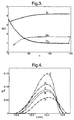
- Figure 2 shows the layer structure of a 51 period (102 layer) optimised Mo/Si stack with a 1.5nm capping layer.
- layer 0 is the substrate surface.
- the optimisation of the Mo/Si stack results in a gradual, smooth variation of the layer thicknesses through the stack while the period width remains nominally constant at about 6.8 to 7.0nm.
- d Mo ⁇ d Si ⁇ 3.5nm varying to d Mo ⁇ 2.7nm and d Si ⁇ 4.2nm near the surface.
- the three component system of examples 8 to 12 is set up initially as a two-component Mo/Si stack with the third material interleaved between the Mo and Si layers with its initial thickness set to zero.
- the global optimisation process then varies the thicknesses of all the layers until a pre-set reflectivity target is approached.
- Mo-Rh/Si and Mo-Ru/Si Mo is favoured near the surface and Rh or Ru near the substrate whereas, in the Mo-RbCl/Si system, RbCl (which is a single entity) partially substitutes for Si in the centre of the stack, i.e. the sum of the thicknesses of the adjacent RbCl and Si layers approaches the thickness of Si in a standard stack.
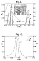
- the layer structure for the Mo-Ru/Si stack is shown in Figure 3.
- This stack has 50 Si layers, including the uppermost layer, and therefore has 148 layers in total, plus a 1.5nm Ru capping layer.
- layer 0 is the substrate surface.
- a 50% gain in computed throughput is observed for the Mo-Ru/Si system over the standard Mo/Si stack.
- Example 12 shows a further improvement in R 9 int for the Mo-Ru/Si system using needle optimisation.
- additional layers of designated materials in this case, Mo, Ru and Rh, with vanishingly small thicknesses, are periodically added to the stack. These layers are then allowed to grow or be rejected by a local optimisation process.
- the needle-optimised stack therefore also contains Rh and additional layers of Mo, the net result of which is a 59% increase in R 9 int compared to the standard stack. It is also worth noting that in this case R 9 int > R 9 peak with the peak reflectivity of 0.764 only marginally lower than for the standard optimised Mo-Ru/Si stack.
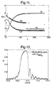
- Fig. 4 is a graph showing R 9 vs. wavelength in the 13.4nm region.
- Line A is for the standard Mo/Si stack, reference example 1; B is optimised Mo/Si, example 4; C is Mo-Ru/Si needle optimised, example 12; D is Mo-Ru-Sr/Si needle optimised, example 19, and E is Mo/Rb optimised, example 22.
- Rh-Mo/Si may be used instead of Mo-Rh/Si and Ru-Mo/Si instead of Mo-Ru/Si
- FIG. 5 shows the layer thicknesses (nm) of a 50 period Mo-Ru-Sr/Si stack with a Ru capping layer.
- layer 0 indicates the substrate surface.
- the spikes in the Mo layer thickness profile indicate layers where the Ru layer has been wholly replaced by Mo as suggested by the numerical optimisation technique. This is not essential to the gain in R 9 int and the relevant Mo layers can be replaced by pairs of Mo and Ru layers.
- Sr performs a similar function to Si in the stack as it has a high value of n and a low extinction coefficient, k , (see Table 1).
- k a low extinction coefficient
- the low absorption within the Sr layers makes it preferable in the top half of the stack.
- the sums of the thicknesses of Si and Sr and Ru and Mo approximate respectively to the optimised Si and Mo thicknesses shown in Figure 2.
- the preferred order of the elements is: Ru-Mo-Sr-Si.
- the grouping of layers may also be varied, e.g. Ru-Mo-Sr/Si may be regarded as Ru-Mo/Sr-Si for calculation purposes.
- Figure 6 shows the layer thicknesses of a needle-optimised 50 period (50 Si layers) Mo-Ru-Sr/Si stack. Rh is included only in the lower half of the stack and predominantly in the first 40 layers. In the lowest layers Rh is preferred over Ru because of its higher optical contrast with Si, in spite of its higher extinction coefficient.
- Sr and Y are less easily depositable owing to the complex chemistry of Y and the high reactivity of Sr, so are less preferred, but still show advantages over the conventional stack.
- Mo-Ru-Zr/Si and Mo-Ru-RbCl/Si show particular promise, as do the same layers in the order Ru-Mo-Zr/Si and Ru-Mo-RbCl/Si.
- Table 3 corresponds to Table 2 but gives data for examples 25 to 40 according to the invention which are reflector stacks tuned for use at 11.3nm.
- Ru and Rh are preferred to Mo for the 11.3nm window.
- the Ru/Be stack has a relative optical throughput greater by up to 70% compared to the Mo/Be reference example, whilst the throughput of the Rh/Be stack is 33% greater. Although this is significantly lower than for Ru/Be, this combination may be preferable in some applications of the invention due to factors such as Rh-Be interface chemistry.
- a particularly preferred embodiment of the invention is the "needle" optimised Rh/Be stack which exhibits a huge increase in reflectivity. This is due to the incorporation of Pd, Ru and Mo layers during the optimisation process effectively transforming it into a Rh-Ru-Pd-Mo/Be or Pd-Rh-Ru-Mo/Be multi-component stack.
- Fig. 8 Selected spectra of Be-based multilayers are shown in Fig. 8. This Figure shows plots of R 9 vs. wavelength in the 11.3nm region for five stacks.
- A is the reference Mo/Be stack
- B is an optimised Mo/Be stack with a Ru capping layer
- C is an optimised Ru/Be stack
- D is a needle optimised Rh/Be stack
- E is an optimised, Ru-capped Ru-Sr/Be stack.
- Examples 35 to 40 are strontium-containing three component systems which yield throughput enhancements of up to a factor of 2.
- Rh and Ru are optimum for this wavelength region and give an increase of 0.7- 1.0% in R.
- Rh(Ru) predominating over Mo near the substrate and vice-versa near the surface This may be because at 13.4nm Rh and Ru exhibit a higher optical contrast with Si than does Mo whereas the extinction coefficient k , and therefore the absorption within the layer, is lower for Mo than Rh and Ru.
- Near the surface of the stack it is important that there be low absorption so that the incident radiation penetrates as deep into the stack as possible so that the phasor addition is maximised. However, deep within the stack where the intensity is low, increased optical contrast is favoured for the reflected intensity to be maximised.
- Examples 41 to 44 are designed for use with a Xenon-jet laser-induced plasma source (Xe-Jet LPS) which has a peak output intensity at about 10.9nm, somewhat lower than the range for which the reflectors described above were designed.
- Xe-Jet LPS Xenon-jet laser-induced plasma source
- Figure 9 shows the R 9 reflectivities (left axis) of various reflectors and the relative Xe-jet LPS emission intensity (right axis) vs. wavelength in nm (X axis).
- Figure 9 shows the R 9 reflectivities (left axis) of various reflectors and the relative Xe-jet LPS emission intensity (right axis) vs. wavelength in nm (X axis).
- examples 44 to 43 have lower R 9 peak and R 9 int than other examples described above, they have the advantage of providing their peak reflectivity very close to the emission maximum of the Xe-Jet LPS. They are thus ideal for use with this source.
- examples 41(g), 42(h) and 43(i) provide relative throughputs of 3.0, 5.7, and 6.5 respectively. This also compares well with the throughput of the Mo/Be stack (d), which is 5.7 and avoids the use of Be, which is highly toxic.
- Figure 10 shows the full wavelength dependence of R (left axis) and R 9 (right axis) of example 44 in the 10 to 12nm range.
- Figure 11 shows layer thicknesses in this stack.
- Example 45 is a three layer stack of Ru-Nb/Si, which demonstrates that Niobium can also give improvements in an Si-based stack, but is otherwise the same as the examples 8 to 12 of Table 2.
- the lanthanides may provide good optical contrast with metals such as Mo, Ru and Rh and may be preferred in reflectors nearer the substrate. In this position, optical contrast is provided because the lanthanides have a refractive index n very close to unity which outweighs the disadvantage that their values of extinction coefficient k are not as low as some other materials in the 9-16nm region. Lanthanum is particularly preferred at or near 13nm.
- porous materials such as low density (porous) silica (aerogel) having a density about 1 tenth that of bulk silica.
- Figure 12 shows the wavelength sensitivity of a Rh-Ru/SiO 2 -aero stack using such porous silica. Its relatively broad reflectance peak below 11nm will be noted.
- Other low density materials include: titania and alumina aerogels; nano-porous silicon, meso-porous silicon, nanoclusters of silicon and other semiconductors. These materials may be used to manufacture reflectors tuned to specific wavelengths throughout the 8 to 20nm wavelength range. The materials are useful because the values on n and k are density dependent.
- n With decreasing density the refractive index, n , tends to unity and the extinction coefficient, k , tends to zero.
- the density of a typical Si aerogel is 0.2gcm -3 whilst that of porous Si is 1.63gcm 3 .
- 49 is a comparative example consisting of an optimised (for 13.4nm) 50 period Mo/Si stack whose outermost layer is 2nm of SiO 2 formed by natural oxidation of the final Si layer in the stack.
- This comparative example forms the reference for relative values of R 9 peak and R 9 int for Examples 50 to 57 of the invention.
- These examples differ from comparative example 49 only in the indicated capping layer, which is deposited on final Si layer of the stack before that layer can oxidise.
- each of palladium (Pd), boron carbide (B 4 C), boron nitride (BN), silicon carbide (SiC), silicon nitride (Si 3 N 4 ) and diamond-like carbon (dl-C) exhibit improved reflectance, or an acceptable reduction, whilst exhibiting a high degree of resistance to chamical attack.
- 58 is a comparative example consisting of an 80 period optimised (for 11.3nm) Mo/Be stack, similarly with an outermost layer of 2nm BeO formed by natural oxidation of the final Be layer.
- This comparative example forms the reference for the relative values of R 9 peak and R 9 int for Examples 59 to 65 of the invention.
- Examples 59 to 65 differ from comparative example 58 in the indicated capping layer which is deposited before the outer Be layer can oxidise. It will again be seen that the layers specified provide improved reflectivity, or an acceptable reduction, whilst exhibiting a high degree of resistance to chemical attack.
- the capping layer includes a modified final layer of the multilayer coating as well as a dedicated capping sub-layer so as to form a bi- or tri-layer protective structure thus increasing the overall thickness of the top layers and reducing the likelihood of incomplete coverage through multiple layer deposition. This is illustrated in Figure 13.
- the reflector of examples 66 to 76 of the invention comprises substrate 10 on which are deposited N periods of alternating layers of a first material 11 and a second material 12.
- first period 13 is shown however all periods save the last are similar.
- the final, N th period comprises a layer 15 of the first material, a layer 16 of a third material and a capping sub-layer 17 of a capping material.
- the first material is denoted X , the second material Y and the third material Z .
- the first material X is one or more of: Mo, Ru, Rh, Nb, Pd, Y and Zr
- the second material Y is one or more of: Be, Si, Sr, Rb, RbCl and P.
- the final period is constructed such that the substance X is chosen as previously, the third material Z on the other hand, is chosen from a set of materials with a moderately high value of refractive index n (>0.96), sufficiently low value of the extinction coefficient k ( ⁇ 0.01), and which are known for their chemical inertness and stability.
- the following materials are suitable: B 4 C, BN, diamond-like C, Si 3 N 4 and SiC.
- the reflectivity loss through absorption in layer 16 may be tolerated in favour of long-term chemical and structural integrity of the multilayer.
- the material of the capping layer 17 has low n such that a large optical contrast is maintained between layers 16 and 17.
- the boundary between layers 16 and 17 also serves to localise the node of the standing wave formed through the superposition of the incident and reflected waves. Suitable materials for capping layer 17 in this configuration are: Ru, Rh, Pd and diamond-like C.
- Table 7 shows layer materials and thicknesses for Examples 66 to 71 which comprise 79 periods of Mo/Be plus the additional period X/Z constructed as described above. These examples are intended for use at 11.3nm.
- Example 66 the whole of the Be layer is oxidized and a Ru capping layer is deposited. This is the reference example.
- Example 67 shows that SiC is not ideal for the 11.3 nm region.
- Examples 70 and 71 show clearly that values of R greater than 75.5% are still possible with such a configuration.
- Rh is used to replace the Mo layer on account of its inertness and C or B 4 C is deposited as layer 16 with an additional coating of Ru as layer 17. This gives a tri-layer of thickness of 7.7 nm forming the protective coating structure.
- Examples 68 and 69 are analogous to 70 and 71 respectively, with the important distinction that the thickness of the layer 17 is increased by 2QW resulting in lower, but still respectable, reflectivity values and with a substantially higher tri-layer thickness of 13.7 n
- Table 8 shows layer materials and thicknesses for Examples 72 to 76 which comprise 49 periods of Mo/Si with the additional period formed by the X/Z combination again terminated with a Ru capping layer.
- the reference example 72 represents a fully oxidised top Si layer upon which a Ru capping layer is applied.
- SiC and B 4 C are the most favorable materials for the Z layer 16.
- Mo cannot be replaced by the more inert metal Rh, therefore a bi-layer protective structure is formed where the combined thickness of layers 16 and 17 ( d Z + d CL ) is about 5.5-6.0 nm.
- the thickness of the SiC layer is increased by 2QW resulting in a 12.6 nm protective bi-layer thickness at the expense of reflectivity.
- capping layer Other suitable materials for the capping layer are Au, MgF 2 , LiF, C 2 F 4 (teflon) and TiN
Landscapes
- Physics & Mathematics (AREA)
- Engineering & Computer Science (AREA)
- General Physics & Mathematics (AREA)
- Chemical & Material Sciences (AREA)
- Nanotechnology (AREA)
- Environmental & Geological Engineering (AREA)
- Epidemiology (AREA)
- Public Health (AREA)
- Health & Medical Sciences (AREA)
- High Energy & Nuclear Physics (AREA)
- General Engineering & Computer Science (AREA)
- Spectroscopy & Molecular Physics (AREA)
- Mathematical Physics (AREA)
- Crystallography & Structural Chemistry (AREA)
- Optics & Photonics (AREA)
- Theoretical Computer Science (AREA)
- Exposure And Positioning Against Photoresist Photosensitive Materials (AREA)
- Exposure Of Semiconductors, Excluding Electron Or Ion Beam Exposure (AREA)
- Optical Elements Other Than Lenses (AREA)
- Surface Treatment Of Optical Elements (AREA)
- Surface Treatment Of Glass (AREA)
- Optical Filters (AREA)
Priority Applications (2)
| Application Number | Priority Date | Filing Date | Title |
|---|---|---|---|
| EP07005669.2A EP1801658B1 (fr) | 1999-07-02 | 2000-06-28 | Sous-couche pour éléments optiques EUV |
| EP00305432A EP1065568B1 (fr) | 1999-07-02 | 2000-06-28 | Appareil de projection lithographique à ultraviolets extrèmes comportant un élément optique avec une couche de recouvrement |
Applications Claiming Priority (5)
| Application Number | Priority Date | Filing Date | Title |
|---|---|---|---|
| EP99305283 | 1999-07-02 | ||
| EP99305283 | 1999-07-02 | ||
| EP99307932 | 1999-10-07 | ||
| EP99307932 | 1999-10-07 | ||
| EP00305432A EP1065568B1 (fr) | 1999-07-02 | 2000-06-28 | Appareil de projection lithographique à ultraviolets extrèmes comportant un élément optique avec une couche de recouvrement |
Related Child Applications (1)
| Application Number | Title | Priority Date | Filing Date |
|---|---|---|---|
| EP07005669.2A Division EP1801658B1 (fr) | 1999-07-02 | 2000-06-28 | Sous-couche pour éléments optiques EUV |
Publications (3)
| Publication Number | Publication Date |
|---|---|
| EP1065568A2 true EP1065568A2 (fr) | 2001-01-03 |
| EP1065568A3 EP1065568A3 (fr) | 2003-03-19 |
| EP1065568B1 EP1065568B1 (fr) | 2007-09-26 |
Family
ID=26153524
Family Applications (3)
| Application Number | Title | Priority Date | Filing Date |
|---|---|---|---|
| EP07005669.2A Expired - Lifetime EP1801658B1 (fr) | 1999-07-02 | 2000-06-28 | Sous-couche pour éléments optiques EUV |
| EP00305432A Expired - Lifetime EP1065568B1 (fr) | 1999-07-02 | 2000-06-28 | Appareil de projection lithographique à ultraviolets extrèmes comportant un élément optique avec une couche de recouvrement |
| EP00305434A Expired - Lifetime EP1065532B1 (fr) | 1999-07-02 | 2000-06-28 | Miroir multicouche à reflectivité ameliorée dans l'ultraviolet extrème et appareil de projection lithographique comportant ledit miroir |
Family Applications Before (1)
| Application Number | Title | Priority Date | Filing Date |
|---|---|---|---|
| EP07005669.2A Expired - Lifetime EP1801658B1 (fr) | 1999-07-02 | 2000-06-28 | Sous-couche pour éléments optiques EUV |
Family Applications After (1)
| Application Number | Title | Priority Date | Filing Date |
|---|---|---|---|
| EP00305434A Expired - Lifetime EP1065532B1 (fr) | 1999-07-02 | 2000-06-28 | Miroir multicouche à reflectivité ameliorée dans l'ultraviolet extrème et appareil de projection lithographique comportant ledit miroir |
Country Status (6)
| Country | Link |
|---|---|
| US (4) | US6449086B1 (fr) |
| EP (3) | EP1801658B1 (fr) |
| JP (2) | JP4068285B2 (fr) |
| KR (2) | KR100589240B1 (fr) |
| DE (2) | DE60018328T2 (fr) |
| TW (2) | TWI267704B (fr) |
Cited By (33)
| Publication number | Priority date | Publication date | Assignee | Title |
|---|---|---|---|---|
| EP1204002A2 (fr) | 2000-11-01 | 2002-05-08 | TRW Inc. | Système de lithographie à l'ultraviolet extrême avec revêtement en film mince pour protection contre le plasma produit par laser |
| WO2003005377A2 (fr) * | 2001-07-03 | 2003-01-16 | The Regents Of The University Of California | Bicouche de finition a l'etat passif |
| WO2003032329A1 (fr) * | 2001-10-04 | 2003-04-17 | Carl Zeiss Smt Ag | Element optique, procede de fabrication de celui-ci, appareil lithographique et procede de fabrication d'un dispositif a semi-conducteurs |
| EP1351258A1 (fr) * | 2002-03-04 | 2003-10-08 | Fraunhofer-Gesellschaft zur Förderung der angewandten Forschung e.V. | Système optique comprenant une source de rayonnement ultraviolet extrême et un élément réflectif |
| US6656575B2 (en) | 2000-03-31 | 2003-12-02 | Carl-Zeiss-Stiftung | Multilayer system with protecting layer system and production method |
| EP1394815A1 (fr) * | 2002-08-28 | 2004-03-03 | ASML Netherlands B.V. | Appareil de lithographie comprenant une multicouche Mo/Si couvert par une couche protectrice |
| US6780496B2 (en) | 2001-07-03 | 2004-08-24 | Euv Llc | Optimized capping layers for EUV multilayers |
| WO2005013003A2 (fr) * | 2003-07-31 | 2005-02-10 | Intel Corporation | Decoupes de masque reflechissant et multicouche de lithographie dans l'ultraviolet extreme |
| US6954257B2 (en) | 2002-08-28 | 2005-10-11 | Asml Netherlands B.V. | Lithographic apparatus and device manufacturing method |
| US7126671B2 (en) | 2003-04-04 | 2006-10-24 | Asml Netherlands B.V. | Lithographic apparatus and device manufacturing method |
| US7239443B2 (en) | 2004-01-16 | 2007-07-03 | Euv Llc | Condenser optic with sacrificial reflective surface |
| US7261957B2 (en) | 2000-03-31 | 2007-08-28 | Carl Zeiss Smt Ag | Multilayer system with protecting layer system and production method |
| WO2007129890A1 (fr) * | 2006-05-05 | 2007-11-15 | Asml Netherlands B.V. | Revêtement anti-réflexion pour masque euv |
| US7420653B2 (en) * | 2003-10-02 | 2008-09-02 | Asml Netherlands B.V. | Lithographic projection apparatus, mirror, method of supplying a protective cap layer, device manufacturing method and device manufactured accordingly |
| US7456932B2 (en) | 2003-07-25 | 2008-11-25 | Asml Netherlands B.V. | Filter window, lithographic projection apparatus, filter window manufacturing method, device manufacturing method and device manufactured thereby |
| US7492443B2 (en) | 2001-06-20 | 2009-02-17 | Asml Netherlands B.V. | Device manufacturing method, device manufactured thereby and a mask for use in the method |
| US7499149B2 (en) | 2003-06-24 | 2009-03-03 | Asml Netherlands B.V. | Holographic mask for lithographic apparatus and device manufacturing method |
| US7541603B2 (en) * | 2006-09-27 | 2009-06-02 | Asml Netherlands B.V. | Radiation system and lithographic apparatus comprising the same |
| WO2009106291A1 (fr) * | 2008-02-27 | 2009-09-03 | Asml Netherlands B V | Elément optique, appareil lithographique comprenant un tel élément optique, procédé de fabrication du dispositif et dispositif fabriqué selon ce procédé |
| US7592610B2 (en) | 2003-10-20 | 2009-09-22 | Asml Netherlands B.V. | Mirror for use in a lithographic apparatus, lithographic apparatus, device manufacturing method, and device manufactured thereby |
| US7598503B2 (en) | 2005-06-13 | 2009-10-06 | Asml Netherlands B.V. | Lithographic apparatus and cleaning method therefor |
| US7701554B2 (en) | 2004-12-29 | 2010-04-20 | Asml Netherlands B.V. | Lithographic apparatus, device manufacturing method, and optical component |
| US7948675B2 (en) | 2005-10-11 | 2011-05-24 | Nikon Corporation | Surface-corrected multilayer-film mirrors with protected reflective surfaces, exposure systems comprising same, and associated methods |
| WO2011068223A1 (fr) | 2009-12-04 | 2011-06-09 | 旭硝子株式会社 | Élément optique pour lithographie par extrême ultraviolet, et procédé de production d'un substrat auquel est fixée une couche réfléchissante pour lithographie par extrême ultraviolet |
| WO2011071086A1 (fr) | 2009-12-09 | 2011-06-16 | 旭硝子株式会社 | Élément optique pour lithographie par ultraviolet extrême (euv) |
| DE102011083461A1 (de) | 2011-09-27 | 2013-03-28 | Carl Zeiss Smt Gmbh | Verfahren zum Erzeugen einer Deckschicht aus Siliziumoxid an einem EUV-Spiegel |
| DE102011083462A1 (de) | 2011-09-27 | 2013-03-28 | Carl Zeiss Smt Gmbh | EUV-Spiegel mit einer Oxynitrid-Deckschicht mit stabiler Zusammensetzung |
| US8537460B2 (en) | 2003-03-03 | 2013-09-17 | Carl Zeiss Smt Gmbh | Reflective optical element and EUV lithography appliance |
| WO2014028483A1 (fr) * | 2012-08-14 | 2014-02-20 | Kla-Tencor Corporation | Systèmes de caractérisation optique utilisant des sources de rayonnement synchrotron compactes |
| WO2014064224A1 (fr) * | 2012-10-25 | 2014-05-01 | Carl Zeiss Smt Gmbh | Système d'exposition par projection s'appliquant à la lithographie euv et procédé de fonctionnement du système d'exposition par projection |
| WO2016168953A1 (fr) * | 2015-04-21 | 2016-10-27 | 中国科学院长春光学精密机械与物理研究所 | Film multicouche présentant une pureté de spectre de l'ultraviolet extrême et une résistance à la dégradation par rayonnement |
| WO2017202579A1 (fr) | 2016-05-24 | 2017-11-30 | Carl Zeiss Smt Gmbh | Élément optique et système de lithographique extrême ultraviolet |
| WO2021037515A1 (fr) * | 2019-08-28 | 2021-03-04 | Carl Zeiss Smt Gmbh | Élément optique et système de lithograhie euv |
Families Citing this family (121)
| Publication number | Priority date | Publication date | Assignee | Title |
|---|---|---|---|---|
| TWI267704B (en) * | 1999-07-02 | 2006-12-01 | Asml Netherlands Bv | Capping layer for EUV optical elements |
| US20070281109A1 (en) * | 2000-03-31 | 2007-12-06 | Carl Zeiss Smt Ag | Multilayer system with protecting layer system and production method |
| JP5371162B2 (ja) * | 2000-10-13 | 2013-12-18 | 三星電子株式会社 | 反射型フォトマスク |
| US6664554B2 (en) * | 2001-01-03 | 2003-12-16 | Euv Llc | Self-cleaning optic for extreme ultraviolet lithography |
| US6576912B2 (en) * | 2001-01-03 | 2003-06-10 | Hugo M. Visser | Lithographic projection apparatus equipped with extreme ultraviolet window serving simultaneously as vacuum window |
| CN1256628C (zh) * | 2001-04-17 | 2006-05-17 | 皇家菲利浦电子有限公司 | 远紫外线可透过的界面结构 |
| US7378673B2 (en) * | 2005-02-25 | 2008-05-27 | Cymer, Inc. | Source material dispenser for EUV light source |
| US7372056B2 (en) * | 2005-06-29 | 2008-05-13 | Cymer, Inc. | LPP EUV plasma source material target delivery system |
| US7439530B2 (en) * | 2005-06-29 | 2008-10-21 | Cymer, Inc. | LPP EUV light source drive laser system |
| US7843632B2 (en) * | 2006-08-16 | 2010-11-30 | Cymer, Inc. | EUV optics |
| US7405416B2 (en) * | 2005-02-25 | 2008-07-29 | Cymer, Inc. | Method and apparatus for EUV plasma source target delivery |
| KR100725859B1 (ko) * | 2001-05-23 | 2007-06-08 | 학교법인 한양학원 | 극자외선 노광 공정용 Ru/Mo/Si 반사형 다층 박막미러 |
| US20030064161A1 (en) * | 2001-06-06 | 2003-04-03 | Malinowski Michael E. | Method for reducing carbon contamination of multilayer mirrors |
| KR100454081B1 (ko) * | 2001-12-24 | 2004-10-20 | 학교법인 한양학원 | 반사형 다층 박막 미러 및 그 제조 방법 |
| US6920199B2 (en) * | 2002-02-20 | 2005-07-19 | Gkss-Forschungszentrum Geesthacht Gmbh | Mirror element for the reflection of x-rays |
| DE10208705B4 (de) | 2002-02-25 | 2008-10-30 | Fraunhofer-Gesellschaft zur Förderung der angewandten Forschung e.V. | Monochromatorspiegel für den EUV-Spektralbereich |
| US20050111083A1 (en) * | 2002-03-27 | 2005-05-26 | Yakshin Andrey E. | Optical broad band element and process for its production |
| KR100455383B1 (ko) * | 2002-04-18 | 2004-11-06 | 삼성전자주식회사 | 반사 포토마스크, 반사 포토마스크의 제조방법 및 이를이용한 집적회로 제조방법 |
| TWI227380B (en) | 2002-06-06 | 2005-02-01 | Asml Netherlands Bv | Lithographic apparatus and device manufacturing method |
| EP1369744A1 (fr) * | 2002-06-06 | 2003-12-10 | ASML Netherlands B.V. | Appareil lithographique et méthode de fabrication d'un dispositif |
| TWI249651B (en) * | 2002-06-14 | 2006-02-21 | Asml Netherlands Bv | EUV lithographic projection apparatus comprising an optical element with a self-assembled monolayer, optical element with a self-assembled monolayer, method of applying a self-assembled monolayer, device manufacturing method and device manufactured there |
| DE10235255B4 (de) * | 2002-08-01 | 2004-08-12 | Infineon Technologies Ag | Reflektierender Spiegel zur lithographischen Belichtung und Herstellungsverfahren |
| US6763086B2 (en) * | 2002-09-05 | 2004-07-13 | Osmic, Inc. | Method and apparatus for detecting boron in x-ray fluorescence spectroscopy |
| DE10258709A1 (de) * | 2002-12-12 | 2004-07-01 | Carl Zeiss Smt Ag | Schutzsystem für reflektive optische Elemente, reflektives optisches Element und Verfahren zu deren Herstellung |
| US6982133B2 (en) * | 2002-12-21 | 2006-01-03 | Intel Corporation | Damage-resistant coatings for EUV lithography components |
| TWI286674B (en) | 2002-12-27 | 2007-09-11 | Asml Netherlands Bv | Container for a mask, method of transferring lithographic masks therein and method of scanning a mask in a container |
| DE10319005A1 (de) * | 2003-04-25 | 2004-11-25 | Carl Zeiss Smt Ag | Reflektives optisches Element, optisches System und EUV-Lithographievorrichtung |
| JP4521696B2 (ja) * | 2003-05-12 | 2010-08-11 | Hoya株式会社 | 反射多層膜付き基板及び反射型マスクブランクス並びに反射型マスク |
| EP1496521A1 (fr) * | 2003-07-09 | 2005-01-12 | ASML Netherlands B.V. | Miroir et appareil lithographique avec miroir |
| JP2005056943A (ja) * | 2003-08-08 | 2005-03-03 | Canon Inc | X線多層ミラーおよびx線露光装置 |
| EP1675164B2 (fr) * | 2003-10-15 | 2019-07-03 | Nikon Corporation | Miroir a films multicouches, procede de production d'un miroir a films multicouches, et systeme d'exposition |
| US20050109278A1 (en) * | 2003-11-26 | 2005-05-26 | Ted Liang | Method to locally protect extreme ultraviolet multilayer blanks used for lithography |
| US7460206B2 (en) * | 2003-12-19 | 2008-12-02 | Carl Zeiss Smt Ag | Projection objective for immersion lithography |
| US7193228B2 (en) | 2004-03-10 | 2007-03-20 | Cymer, Inc. | EUV light source optical elements |
| JP4693395B2 (ja) * | 2004-02-19 | 2011-06-01 | Hoya株式会社 | 反射型マスクブランクス及び反射型マスク並びに半導体装置の製造方法 |
| US7196342B2 (en) * | 2004-03-10 | 2007-03-27 | Cymer, Inc. | Systems and methods for reducing the influence of plasma-generated debris on the internal components of an EUV light source |
| JP4566791B2 (ja) * | 2004-03-26 | 2010-10-20 | キヤノン株式会社 | 軟x線多層膜反射鏡 |
| JP4532991B2 (ja) * | 2004-05-26 | 2010-08-25 | キヤノン株式会社 | 投影光学系、露光装置及びデバイス製造方法 |
| US7491478B2 (en) * | 2004-07-23 | 2009-02-17 | Asml Netherlands B.V. | Lithographic apparatus and device manufacturing method |
| US20060024589A1 (en) | 2004-07-28 | 2006-02-02 | Siegfried Schwarzl | Passivation of multi-layer mirror for extreme ultraviolet lithography |
| DE102004043516A1 (de) | 2004-09-08 | 2006-03-23 | Osram Opto Semiconductors Gmbh | Seitlich emittierendes strahlungserzeugendes Bauelement und Linse für ein solches Bauelement |
| US7092290B2 (en) * | 2004-11-16 | 2006-08-15 | Sandisk Corporation | High speed programming system with reduced over programming |
| DE102004062289B4 (de) | 2004-12-23 | 2007-07-19 | Fraunhofer-Gesellschaft zur Förderung der angewandten Forschung e.V. | Thermisch stabiler Multilayer-Spiegel für den EUV-Spektralbereich |
| US7196343B2 (en) * | 2004-12-30 | 2007-03-27 | Asml Netherlands B.V. | Optical element, lithographic apparatus including such an optical element, device manufacturing method, and device manufactured thereby |
| US7450217B2 (en) | 2005-01-12 | 2008-11-11 | Asml Netherlands B.V. | Exposure apparatus, coatings for exposure apparatus, lithographic apparatus, device manufacturing method, and device manufactured thereby |
| US7449703B2 (en) * | 2005-02-25 | 2008-11-11 | Cymer, Inc. | Method and apparatus for EUV plasma source target delivery target material handling |
| US7482609B2 (en) * | 2005-02-28 | 2009-01-27 | Cymer, Inc. | LPP EUV light source drive laser system |
| US7336416B2 (en) * | 2005-04-27 | 2008-02-26 | Asml Netherlands B.V. | Spectral purity filter for multi-layer mirror, lithographic apparatus including such multi-layer mirror, method for enlarging the ratio of desired radiation and undesired radiation, and device manufacturing method |
| US7495743B2 (en) * | 2005-09-30 | 2009-02-24 | International Business Machines Corporation | Immersion optical lithography system having protective optical coating |
| EP1947682B1 (fr) * | 2005-10-11 | 2012-01-18 | Nikon Corporation | Miroir réflecteur multicouche, procédé de fabrication d'un miroir réflecteur multicouche, système optique, appareil d'exposition et procédé de fabrication d'un dispositif |
| JP5045144B2 (ja) * | 2007-02-22 | 2012-10-10 | 株式会社ニコン | 多層膜反射鏡、露光装置、デバイス製造方法、及び多層膜反射鏡の製造方法 |
| US7453077B2 (en) * | 2005-11-05 | 2008-11-18 | Cymer, Inc. | EUV light source |
| JP2007134464A (ja) * | 2005-11-09 | 2007-05-31 | Canon Inc | 多層膜を有する光学素子及びそれを有する露光装置 |
| JP2007140105A (ja) * | 2005-11-18 | 2007-06-07 | Nikon Corp | 多層膜反射鏡及び露光装置 |
| JP2007234822A (ja) * | 2006-02-28 | 2007-09-13 | Canon Inc | 露光装置及びその制御方法並びにデバイス製造方法 |
| JP4946296B2 (ja) | 2006-03-30 | 2012-06-06 | 凸版印刷株式会社 | 反射型フォトマスクブランク及びその製造方法、反射型フォトマスク、並びに、半導体装置の製造方法 |
| JP5200327B2 (ja) * | 2006-03-31 | 2013-06-05 | 凸版印刷株式会社 | 反射型フォトマスクブランク及びその製造方法、反射型フォトマスク及びその製造方法、並びに、極端紫外光の露光方法 |
| US7723704B2 (en) * | 2006-11-10 | 2010-05-25 | Globalfoundries Inc. | EUV pellicle with increased EUV light transmittance |
| JP4365855B2 (ja) * | 2006-12-21 | 2009-11-18 | 三菱電機株式会社 | 車両用操舵装置 |
| TWI427334B (zh) * | 2007-02-05 | 2014-02-21 | Zeiss Carl Smt Gmbh | Euv蝕刻裝置反射光學元件 |
| US7663127B2 (en) * | 2007-03-13 | 2010-02-16 | Globalfoundries Inc. | EUV debris mitigation filter and method for fabricating semiconductor dies using same |
| JP2008263173A (ja) * | 2007-03-16 | 2008-10-30 | Canon Inc | 露光装置 |
| ATE512389T1 (de) | 2007-10-23 | 2011-06-15 | Imec | Erkennung von kontaminationen in euv-systemen |
| TWI425252B (zh) * | 2008-03-26 | 2014-02-01 | Nat Applied Res Laboratories | 反射膜及其製成方法 |
| KR100972863B1 (ko) * | 2008-04-22 | 2010-07-28 | 주식회사 하이닉스반도체 | 극자외선 리소그라피 마스크 및 그 제조 방법 |
| DE102009001488A1 (de) | 2008-05-21 | 2009-11-26 | Asml Netherlands B.V. | Entfernen von Kontaminationen von optischen Oberflächen durch aktivierten Wasserstoff |
| US20110080573A1 (en) * | 2008-06-04 | 2011-04-07 | Asml Netherlands B.V. | Multilayer mirror and lithographic apparatus |
| DE102008002403A1 (de) * | 2008-06-12 | 2009-12-17 | Carl Zeiss Smt Ag | Verfahren zum Herstellen einer Mehrlagen-Beschichtung, optisches Element und optische Anordnung |
| JP2011527436A (ja) | 2008-07-07 | 2011-10-27 | コーニンクレッカ フィリップス エレクトロニクス エヌ ヴィ | スパッタ耐性材料を含む極紫外線放射反射要素 |
| EP2157584A3 (fr) * | 2008-08-14 | 2011-07-13 | ASML Netherlands B.V. | Source de radiation, appareil de lithographie et procédé de fabrication d'un dispositif |
| NL2003363A (en) * | 2008-09-10 | 2010-03-15 | Asml Netherlands Bv | Lithographic apparatus, method of manufacturing an article for a lithographic apparatus and device manufacturing method. |
| DE102009017095A1 (de) * | 2009-04-15 | 2010-10-28 | Carl Zeiss Smt Ag | Spiegel für den EUV-Wellenlängenbereich, Projektionsobjektiv für die Mikrolithographie mit einem solchen Spiegel und Projektionsbelichtungsanlage für die Mikrolithographie mit einem solchen Projektionsobjektiv |
| EP2348347A3 (fr) * | 2009-08-28 | 2012-07-04 | European Space Agency | Procédé d'assemblage de plusieures piles à plaque-miroir en un ensemble rigide |
| NL2005460A (en) * | 2009-11-20 | 2011-05-23 | Asml Netherlands Bv | Multilayer mirror, lithographic apparatus, and methods for manufacturing a multilayer mirror and a product. |
| CN102621815B (zh) * | 2011-01-26 | 2016-12-21 | Asml荷兰有限公司 | 用于光刻设备的反射光学部件及器件制造方法 |
| WO2012136420A1 (fr) | 2011-04-04 | 2012-10-11 | Asml Netherlands B.V. | Miroir, collecteur d'une source de rayonnement et appareil lithographique |
| DE102011076011A1 (de) * | 2011-05-18 | 2012-11-22 | Carl Zeiss Smt Gmbh | Reflektives optisches Element und optisches System für die EUV-Lithographie |
| WO2012171674A1 (fr) * | 2011-06-15 | 2012-12-20 | Asml Netherlands B.V. | Miroir multicouche, procédé de production d'un miroir multicouche et appareil lithographique |
| US10185234B2 (en) * | 2012-10-04 | 2019-01-22 | Asml Netherlands B.V. | Harsh environment optical element protection |
| DE102012222466A1 (de) * | 2012-12-06 | 2014-06-12 | Carl Zeiss Smt Gmbh | Reflektives optisches Element für die EUV-Lithographie |
| US20140158914A1 (en) * | 2012-12-11 | 2014-06-12 | Sandia Corporation | Optical component with blocking surface and method thereof |
| US20140168758A1 (en) * | 2012-12-13 | 2014-06-19 | Kla-Tencor Corporation | Carbon as grazing incidence euv mirror and spectral purity filter |
| DE102013200294A1 (de) * | 2013-01-11 | 2014-07-17 | Carl Zeiss Smt Gmbh | EUV-Spiegel und optisches System mit EUV-Spiegel |
| US9632411B2 (en) | 2013-03-14 | 2017-04-25 | Applied Materials, Inc. | Vapor deposition deposited photoresist, and manufacturing and lithography systems therefor |
| US9354508B2 (en) | 2013-03-12 | 2016-05-31 | Applied Materials, Inc. | Planarized extreme ultraviolet lithography blank, and manufacturing and lithography systems therefor |
| RU2522448C1 (ru) * | 2013-03-13 | 2014-07-10 | Открытое акционерное общество "Научно-исследовательский и технологический институт оптического материаловедения Всероссийского научного центра "Государственный оптический институт им. С.И. Вавилова" (ОАО "НИТИОМ ВНЦ "ГОИ им. С.И. Вавилова") | Покрытие для заготовки космического зеркала |
| KR20180050760A (ko) * | 2013-05-09 | 2018-05-15 | 가부시키가이샤 니콘 | 광학 소자, 투영 광학계, 노광 장치 및 디바이스 제조 방법 |
| WO2015039705A1 (fr) | 2013-09-23 | 2015-03-26 | Carl Zeiss Smt Gmbh | Miroir multicouche |
| TWI565681B (zh) | 2013-10-15 | 2017-01-11 | 中原大學 | 多孔二氧化矽氣凝膠複合薄膜及其製造方法以及二氧化碳吸收裝置 |
| DE102014200932A1 (de) | 2014-01-20 | 2015-07-23 | Carl Zeiss Smt Gmbh | EUV-Spiegel und optisches System mit EUV-Spiegel |
| US9612522B2 (en) * | 2014-07-11 | 2017-04-04 | Applied Materials, Inc. | Extreme ultraviolet mask blank production system with thin absorber and manufacturing system therefor |
| US9581890B2 (en) | 2014-07-11 | 2017-02-28 | Applied Materials, Inc. | Extreme ultraviolet reflective element with multilayer stack and method of manufacturing thereof |
| DE102015207140A1 (de) * | 2015-04-20 | 2016-10-20 | Carl Zeiss Smt Gmbh | Spiegel, insbesondere für eine mikrolithographische Projektionsbelichtungsanlage |
| TWI769137B (zh) * | 2015-06-30 | 2022-07-01 | 蘇普利亞 傑西瓦爾 | 一種用於紫外、極紫外和軟x射線光學元件的塗層及其製備方法 |
| JP2017026928A (ja) * | 2015-07-27 | 2017-02-02 | エヌ・ティ・ティ・アドバンステクノロジ株式会社 | Euv光用多層膜反射鏡 |
| DE102016200814A1 (de) | 2016-01-21 | 2017-07-27 | Carl Zeiss Smt Gmbh | Reflektives optisches Element und optisches System für die EUV-Lithographie |
| TWI811037B (zh) | 2016-07-27 | 2023-08-01 | 美商應用材料股份有限公司 | 具多層吸收劑的極紫外遮罩坯料及製造方法 |
| DE102016218028A1 (de) | 2016-09-20 | 2018-03-22 | Carl Zeiss Smt Gmbh | Reflektives optisches Element |
| DE102017206118A1 (de) * | 2017-04-10 | 2018-04-19 | Carl Zeiss Smt Gmbh | Reflektives optisches Element und optisches System |
| US11086209B2 (en) * | 2017-04-27 | 2021-08-10 | Taiwan Semiconductor Manufacturing Co., Ltd. | EUV lithography mask with a porous reflective multilayer structure |
| DE102017213181A1 (de) | 2017-07-31 | 2019-01-31 | Carl Zeiss Smt Gmbh | Optische Anordnung für EUV-Strahlung mit einer Abschirmung zum Schutz vor der Ätzwirkung eines Plasmas |
| US11268911B2 (en) * | 2019-01-04 | 2022-03-08 | Kla-Tencor Corporation | Boron-based capping layers for EUV optics |
| TW202043905A (zh) | 2019-03-01 | 2020-12-01 | 美商應用材料股份有限公司 | 物理氣相沉積系統與處理 |
| CN110221369B (zh) * | 2019-06-26 | 2020-10-27 | 西安交通大学 | 一种基于BN(Al)薄膜的布拉格反射镜及制备方法 |
| KR20210089406A (ko) | 2020-01-08 | 2021-07-16 | 주식회사 에스앤에스텍 | 극자외선용 반사형 블랭크 마스크 및 포토마스크 |
| US11630385B2 (en) | 2020-01-24 | 2023-04-18 | Applied Materials, Inc. | Extreme ultraviolet mask absorber materials |
| TW202131087A (zh) | 2020-01-27 | 2021-08-16 | 美商應用材料股份有限公司 | 極紫外光遮罩吸收劑材料 |
| TW202141165A (zh) | 2020-03-27 | 2021-11-01 | 美商應用材料股份有限公司 | 極紫外光遮罩吸收材料 |
| US11143604B1 (en) | 2020-04-06 | 2021-10-12 | Kla Corporation | Soft x-ray optics with improved filtering |
| TWI836207B (zh) | 2020-04-17 | 2024-03-21 | 美商應用材料股份有限公司 | 極紫外光遮罩吸收材料 |
| DE102020206117A1 (de) | 2020-05-14 | 2021-11-18 | Carl Zeiss Smt Gmbh | Optisches Element, EUV-Lithographiesystem und Verfahren zum Bilden von Nanopartikeln |
| TW202202641A (zh) | 2020-07-13 | 2022-01-16 | 美商應用材料股份有限公司 | 極紫外線遮罩吸收劑材料 |
| US11609490B2 (en) | 2020-10-06 | 2023-03-21 | Applied Materials, Inc. | Extreme ultraviolet mask absorber materials |
| KR20220075021A (ko) | 2020-11-26 | 2022-06-07 | 삼성전자주식회사 | 극자외선 발생 장치와 이의 제조 방법, 및 극자외선 시스템 |
| US11513437B2 (en) | 2021-01-11 | 2022-11-29 | Applied Materials, Inc. | Extreme ultraviolet mask absorber materials |
| US11592738B2 (en) | 2021-01-28 | 2023-02-28 | Applied Materials, Inc. | Extreme ultraviolet mask absorber materials |
| US20220382148A1 (en) * | 2021-05-28 | 2022-12-01 | Taiwan Semiconductor Manufacturing Co., Ltd. | Extreme ultraviolet mask with alloy based absorbers |
| US11762278B2 (en) | 2021-06-16 | 2023-09-19 | Applied Materials, Inc. | Multilayer extreme ultraviolet reflectors |
| US11815803B2 (en) | 2021-08-30 | 2023-11-14 | Applied Materials, Inc. | Multilayer extreme ultraviolet reflector materials |
| US11782337B2 (en) | 2021-09-09 | 2023-10-10 | Applied Materials, Inc. | Multilayer extreme ultraviolet reflectors |
| DE102022203495A1 (de) * | 2022-04-07 | 2023-10-12 | Carl Zeiss Smt Gmbh | Reflektives optisches Element für eine Wellenlänge im extrem ultravioletten Wellenlängenbereich |
Citations (4)
| Publication number | Priority date | Publication date | Assignee | Title |
|---|---|---|---|---|
| US5433988A (en) * | 1986-10-01 | 1995-07-18 | Canon Kabushiki Kaisha | Multi-layer reflection mirror for soft X-ray to vacuum ultraviolet ray |
| WO1998028665A1 (fr) * | 1996-12-24 | 1998-07-02 | Koninklijke Philips Electronics N.V. | Dispositif de positionnement bidimensionnellement equilibre a deux porte-objets, et dispositif lithographique comportant ledit dispositif |
| US5850309A (en) * | 1996-03-27 | 1998-12-15 | Nikon Corporation | Mirror for high-intensity ultraviolet light beam |
| EP0905565A1 (fr) * | 1997-09-30 | 1999-03-31 | Siemens Aktiengesellschaft | Amélioration pour la photolithographie à UV lointains |
Family Cites Families (35)
| Publication number | Priority date | Publication date | Assignee | Title |
|---|---|---|---|---|
| US4214818A (en) * | 1978-11-08 | 1980-07-29 | Westinghouse Electric Corp. | Hot pressed SiC-high power laser mirror |
| JP2566564B2 (ja) | 1986-10-01 | 1996-12-25 | キヤノン株式会社 | 軟x線又は真空紫外線用多層膜反射鏡 |
| JPS63106703A (ja) | 1986-10-24 | 1988-05-11 | Nikon Corp | 光学素子 |
| US4778251A (en) * | 1987-03-09 | 1988-10-18 | Rockwell International Corporation | Thickness error compensation for digital gradient-index optical coatings |
| JPH0795120B2 (ja) * | 1987-07-13 | 1995-10-11 | 日本航空電子工業株式会社 | 多層膜反射鏡 |
| JPH0213902A (ja) | 1988-07-01 | 1990-01-18 | Mitsubishi Electric Corp | 紫外光反射板 |
| JP2883100B2 (ja) * | 1989-05-22 | 1999-04-19 | キヤノン株式会社 | 軟x線・真空紫外線用ハーフミラー又はビームスプリッター |
| JP2787987B2 (ja) * | 1989-11-22 | 1998-08-20 | 株式会社リコー | 反射鏡 |
| US5265143A (en) * | 1993-01-05 | 1993-11-23 | At&T Bell Laboratories | X-ray optical element including a multilayer coating |
| US5356662A (en) * | 1993-01-05 | 1994-10-18 | At&T Bell Laboratories | Method for repairing an optical element which includes a multilayer coating |
| US5591958A (en) * | 1993-06-14 | 1997-01-07 | Nikon Corporation | Scanning exposure method and apparatus |
| US5360659A (en) * | 1993-05-24 | 1994-11-01 | The Dow Chemical Company | Two component infrared reflecting film |
| US5513039A (en) * | 1993-05-26 | 1996-04-30 | Litton Systems, Inc. | Ultraviolet resistive coated mirror and method of fabrication |
| DE4407502A1 (de) * | 1994-03-07 | 1995-09-14 | Leybold Ag | Mehrlagige Beschichtung |
| JP3345512B2 (ja) | 1994-07-12 | 2002-11-18 | 株式会社日立製作所 | 半導体装置の製造方法 |
| US5646976A (en) * | 1994-08-01 | 1997-07-08 | Osmic, Inc. | Optical element of multilayered thin film for X-rays and neutrons |
| US5521031A (en) | 1994-10-20 | 1996-05-28 | At&T Corp. | Pattern delineating apparatus for use in the EUV spectrum |
| JPH08220304A (ja) * | 1995-02-13 | 1996-08-30 | Tadahiro Omi | 光学物品及びそれを用いた露光装置又は光学系並びにその製造方法 |
| JP2658966B2 (ja) * | 1995-04-20 | 1997-09-30 | 日本電気株式会社 | フォトマスク及びその製造方法 |
| US5789320A (en) * | 1996-04-23 | 1998-08-04 | International Business Machines Corporation | Plating of noble metal electrodes for DRAM and FRAM |
| JPH10199801A (ja) * | 1997-01-13 | 1998-07-31 | Mitsubishi Materials Corp | 人工ダイヤモンド膜の残留応力が少ないx線リソグラフィー用マスク |
| US5911858A (en) | 1997-02-18 | 1999-06-15 | Sandia Corporation | Method for high-precision multi-layered thin film deposition for deep and extreme ultraviolet mirrors |
| JP3607454B2 (ja) * | 1997-03-31 | 2005-01-05 | Hoya株式会社 | X線マスク用x線透過膜、x線マスクブランク及びx線マスク並びにこれらの製造方法並びに炭化珪素膜の研磨方法 |
| IL132432A0 (en) * | 1997-04-18 | 2001-03-19 | Nikon Corp | An exposure apparatus exposure method using the same and method of manufacture of circuit device |
| US6268904B1 (en) * | 1997-04-23 | 2001-07-31 | Nikon Corporation | Optical exposure apparatus and photo-cleaning method |
| JPH1138192A (ja) * | 1997-07-17 | 1999-02-12 | Nikon Corp | 多層膜反射鏡 |
| US5958605A (en) * | 1997-11-10 | 1999-09-28 | Regents Of The University Of California | Passivating overcoat bilayer for multilayer reflective coatings for extreme ultraviolet lithography |
| US6042995A (en) | 1997-12-09 | 2000-03-28 | Lucent Technologies Inc. | Lithographic process for device fabrication using a multilayer mask which has been previously inspected |
| US6391400B1 (en) * | 1998-04-08 | 2002-05-21 | Thomas A. Russell | Thermal control films suitable for use in glazing |
| WO2000020928A1 (fr) * | 1998-10-08 | 2000-04-13 | Rochester Institute Of Technology | Photomasque pour gravure par projection inferieure ou egale a 160 nm environ, et procede correspondant |
| US6229652B1 (en) * | 1998-11-25 | 2001-05-08 | The Regents Of The University Of California | High reflectance and low stress Mo2C/Be multilayers |
| US6013399A (en) * | 1998-12-04 | 2000-01-11 | Advanced Micro Devices, Inc. | Reworkable EUV mask materials |
| US6180291B1 (en) * | 1999-01-22 | 2001-01-30 | International Business Machines Corporation | Static resistant reticle |
| TWI267704B (en) * | 1999-07-02 | 2006-12-01 | Asml Netherlands Bv | Capping layer for EUV optical elements |
| SG124257A1 (en) * | 2000-02-25 | 2006-08-30 | Nikon Corp | Exposure apparatus and exposure method capable of controlling illumination distribution |
-
2000
- 2000-06-20 TW TW089112078A patent/TWI267704B/zh not_active IP Right Cessation
- 2000-06-20 TW TW089112079A patent/TW561279B/zh not_active IP Right Cessation
- 2000-06-28 DE DE60018328T patent/DE60018328T2/de not_active Expired - Lifetime
- 2000-06-28 US US09/605,651 patent/US6449086B1/en not_active Expired - Lifetime
- 2000-06-28 JP JP2000195020A patent/JP4068285B2/ja not_active Expired - Fee Related
- 2000-06-28 JP JP2000194831A patent/JP3652221B2/ja not_active Expired - Fee Related
- 2000-06-28 KR KR1020000035870A patent/KR100589240B1/ko active IP Right Grant
- 2000-06-28 EP EP07005669.2A patent/EP1801658B1/fr not_active Expired - Lifetime
- 2000-06-28 US US09/605,657 patent/US6724462B1/en not_active Ceased
- 2000-06-28 EP EP00305432A patent/EP1065568B1/fr not_active Expired - Lifetime
- 2000-06-28 DE DE60036510T patent/DE60036510T2/de not_active Expired - Lifetime
- 2000-06-28 EP EP00305434A patent/EP1065532B1/fr not_active Expired - Lifetime
- 2000-06-28 KR KR1020000035869A patent/KR100599940B1/ko active IP Right Grant
-
2002
- 2002-07-26 US US10/205,206 patent/US6738188B2/en not_active Expired - Lifetime
-
2006
- 2006-03-28 US US11/390,536 patent/USRE42338E1/en not_active Expired - Lifetime
Patent Citations (4)
| Publication number | Priority date | Publication date | Assignee | Title |
|---|---|---|---|---|
| US5433988A (en) * | 1986-10-01 | 1995-07-18 | Canon Kabushiki Kaisha | Multi-layer reflection mirror for soft X-ray to vacuum ultraviolet ray |
| US5850309A (en) * | 1996-03-27 | 1998-12-15 | Nikon Corporation | Mirror for high-intensity ultraviolet light beam |
| WO1998028665A1 (fr) * | 1996-12-24 | 1998-07-02 | Koninklijke Philips Electronics N.V. | Dispositif de positionnement bidimensionnellement equilibre a deux porte-objets, et dispositif lithographique comportant ledit dispositif |
| EP0905565A1 (fr) * | 1997-09-30 | 1999-03-31 | Siemens Aktiengesellschaft | Amélioration pour la photolithographie à UV lointains |
Non-Patent Citations (1)
| Title |
|---|
| HUDEK P ET AL: "E-beam and RIE examination of chemically amplified positive-tone resist CAMP6" MICROELECTRONIC ENGINEERING, ELSEVIER PUBLISHERS BV., AMSTERDAM, NL, vol. 26, no. 3, 1 November 1995 (1995-11-01), pages 167-179, XP004000099 ISSN: 0167-9317 * |
Cited By (56)
| Publication number | Priority date | Publication date | Assignee | Title |
|---|---|---|---|---|
| US6656575B2 (en) | 2000-03-31 | 2003-12-02 | Carl-Zeiss-Stiftung | Multilayer system with protecting layer system and production method |
| US7261957B2 (en) | 2000-03-31 | 2007-08-28 | Carl Zeiss Smt Ag | Multilayer system with protecting layer system and production method |
| EP1204002A3 (fr) * | 2000-11-01 | 2003-03-26 | TRW Inc. | Système de lithographie à l'ultraviolet extrême avec revêtement en film mince pour protection contre le plasma produit par laser |
| EP1204002A2 (fr) | 2000-11-01 | 2002-05-08 | TRW Inc. | Système de lithographie à l'ultraviolet extrême avec revêtement en film mince pour protection contre le plasma produit par laser |
| US7492443B2 (en) | 2001-06-20 | 2009-02-17 | Asml Netherlands B.V. | Device manufacturing method, device manufactured thereby and a mask for use in the method |
| WO2003005377A2 (fr) * | 2001-07-03 | 2003-01-16 | The Regents Of The University Of California | Bicouche de finition a l'etat passif |
| WO2003005377A3 (fr) * | 2001-07-03 | 2003-10-30 | Univ California | Bicouche de finition a l'etat passif |
| US6780496B2 (en) | 2001-07-03 | 2004-08-24 | Euv Llc | Optimized capping layers for EUV multilayers |
| US7172788B2 (en) | 2001-10-04 | 2007-02-06 | Carl Zeiss Smt Ag | Optical element and method for its manufacture as well as lithography apparatus and method for manufacturing a semiconductor device |
| WO2003032329A1 (fr) * | 2001-10-04 | 2003-04-17 | Carl Zeiss Smt Ag | Element optique, procede de fabrication de celui-ci, appareil lithographique et procede de fabrication d'un dispositif a semi-conducteurs |
| EP1351258A1 (fr) * | 2002-03-04 | 2003-10-08 | Fraunhofer-Gesellschaft zur Förderung der angewandten Forschung e.V. | Système optique comprenant une source de rayonnement ultraviolet extrême et un élément réflectif |
| EP1394815A1 (fr) * | 2002-08-28 | 2004-03-03 | ASML Netherlands B.V. | Appareil de lithographie comprenant une multicouche Mo/Si couvert par une couche protectrice |
| US6954257B2 (en) | 2002-08-28 | 2005-10-11 | Asml Netherlands B.V. | Lithographic apparatus and device manufacturing method |
| US8537460B2 (en) | 2003-03-03 | 2013-09-17 | Carl Zeiss Smt Gmbh | Reflective optical element and EUV lithography appliance |
| US9910193B2 (en) | 2003-03-03 | 2018-03-06 | Carl Zeiss Smt Gmbh | Reflective optical element and EUV lithography appliance |
| US8891163B2 (en) | 2003-03-03 | 2014-11-18 | Carl Zeiss Smt Gmbh | Reflective optical element and EUV lithography appliance |
| US7126671B2 (en) | 2003-04-04 | 2006-10-24 | Asml Netherlands B.V. | Lithographic apparatus and device manufacturing method |
| US7499149B2 (en) | 2003-06-24 | 2009-03-03 | Asml Netherlands B.V. | Holographic mask for lithographic apparatus and device manufacturing method |
| US7776390B2 (en) | 2003-07-25 | 2010-08-17 | Asml Netherlands B.V. | Filter window manufacturing method |
| US7456932B2 (en) | 2003-07-25 | 2008-11-25 | Asml Netherlands B.V. | Filter window, lithographic projection apparatus, filter window manufacturing method, device manufacturing method and device manufactured thereby |
| WO2005013003A2 (fr) * | 2003-07-31 | 2005-02-10 | Intel Corporation | Decoupes de masque reflechissant et multicouche de lithographie dans l'ultraviolet extreme |
| US6998202B2 (en) | 2003-07-31 | 2006-02-14 | Intel Corporation | Multilayer reflective extreme ultraviolet lithography mask blanks |
| WO2005013003A3 (fr) * | 2003-07-31 | 2005-08-11 | Intel Corp | Decoupes de masque reflechissant et multicouche de lithographie dans l'ultraviolet extreme |
| CN1580957B (zh) * | 2003-07-31 | 2010-05-26 | 英特尔公司 | 多层反射远紫外线光刻掩模坯件 |
| US7420653B2 (en) * | 2003-10-02 | 2008-09-02 | Asml Netherlands B.V. | Lithographic projection apparatus, mirror, method of supplying a protective cap layer, device manufacturing method and device manufactured accordingly |
| US7592610B2 (en) | 2003-10-20 | 2009-09-22 | Asml Netherlands B.V. | Mirror for use in a lithographic apparatus, lithographic apparatus, device manufacturing method, and device manufactured thereby |
| US7239443B2 (en) | 2004-01-16 | 2007-07-03 | Euv Llc | Condenser optic with sacrificial reflective surface |
| US7701554B2 (en) | 2004-12-29 | 2010-04-20 | Asml Netherlands B.V. | Lithographic apparatus, device manufacturing method, and optical component |
| US7750326B2 (en) | 2005-06-13 | 2010-07-06 | Asml Netherlands B.V. | Lithographic apparatus and cleaning method therefor |
| US7598503B2 (en) | 2005-06-13 | 2009-10-06 | Asml Netherlands B.V. | Lithographic apparatus and cleaning method therefor |
| US7948675B2 (en) | 2005-10-11 | 2011-05-24 | Nikon Corporation | Surface-corrected multilayer-film mirrors with protected reflective surfaces, exposure systems comprising same, and associated methods |
| US7736820B2 (en) | 2006-05-05 | 2010-06-15 | Asml Netherlands B.V. | Anti-reflection coating for an EUV mask |
| WO2007129890A1 (fr) * | 2006-05-05 | 2007-11-15 | Asml Netherlands B.V. | Revêtement anti-réflexion pour masque euv |
| US7863591B2 (en) | 2006-09-27 | 2011-01-04 | Asml Netherlands B.V. | Radiation system and lithographic apparatus comprising the same |
| US7541603B2 (en) * | 2006-09-27 | 2009-06-02 | Asml Netherlands B.V. | Radiation system and lithographic apparatus comprising the same |
| WO2009106291A1 (fr) * | 2008-02-27 | 2009-09-03 | Asml Netherlands B V | Elément optique, appareil lithographique comprenant un tel élément optique, procédé de fabrication du dispositif et dispositif fabriqué selon ce procédé |
| TWI494703B (zh) * | 2008-02-27 | 2015-08-01 | Asml Netherlands Bv | 光學元件、包括光學元件之微影裝置、器件製造方法以及從其製造之器件 |
| US8345223B2 (en) | 2008-02-27 | 2013-01-01 | Asml Netherlands B.V. | Optical element, lithographic apparatus including such an optical element, device manufacturing method, and device manufactured thereby |
| CN101960338B (zh) * | 2008-02-27 | 2013-01-09 | Asml荷兰有限公司 | 光学元件、包括该光学元件的光刻设备、器件制造方法以及所制造的器件 |
| WO2011068223A1 (fr) | 2009-12-04 | 2011-06-09 | 旭硝子株式会社 | Élément optique pour lithographie par extrême ultraviolet, et procédé de production d'un substrat auquel est fixée une couche réfléchissante pour lithographie par extrême ultraviolet |
| WO2011071086A1 (fr) | 2009-12-09 | 2011-06-16 | 旭硝子株式会社 | Élément optique pour lithographie par ultraviolet extrême (euv) |
| US8986910B2 (en) | 2009-12-09 | 2015-03-24 | Asahi Glass Company, Limited | Optical member for EUV lithography |
| DE102011083461A1 (de) | 2011-09-27 | 2013-03-28 | Carl Zeiss Smt Gmbh | Verfahren zum Erzeugen einer Deckschicht aus Siliziumoxid an einem EUV-Spiegel |
| DE102011083462A1 (de) | 2011-09-27 | 2013-03-28 | Carl Zeiss Smt Gmbh | EUV-Spiegel mit einer Oxynitrid-Deckschicht mit stabiler Zusammensetzung |
| WO2013045310A1 (fr) | 2011-09-27 | 2013-04-04 | Carl Zeiss Smt Gmbh | Procédé de production d'une couche de recouvrement en oxyde de silicium sur un miroir euv, miroir euv, et appareil de lithographie euv |
| WO2013045311A1 (fr) | 2011-09-27 | 2013-04-04 | Carl Zeiss Smt Gmbh | Miroir euv comprenant une couche de recouvrement en oxynitrure de composition stable, appareil de lithographie euv, et procédé de mise en oeuvre |
| US9880476B2 (en) | 2011-09-27 | 2018-01-30 | Carl Zeiss Smt Gmbh | Method for producing a capping layer composed of silicon oxide on an EUV mirror, EUV mirror, and EUV lithography apparatus |
| US9229331B2 (en) | 2011-09-27 | 2016-01-05 | Carl Zeiss Smt Gmbh | EUV mirror comprising an oxynitride capping layer having a stable composition, EUV lithography apparatus, and operating method |
| US8941336B1 (en) | 2012-08-14 | 2015-01-27 | Kla-Tencor Corporation | Optical characterization systems employing compact synchrotron radiation sources |
| US8749179B2 (en) | 2012-08-14 | 2014-06-10 | Kla-Tencor Corporation | Optical characterization systems employing compact synchrotron radiation sources |
| WO2014028483A1 (fr) * | 2012-08-14 | 2014-02-20 | Kla-Tencor Corporation | Systèmes de caractérisation optique utilisant des sources de rayonnement synchrotron compactes |
| WO2014064224A1 (fr) * | 2012-10-25 | 2014-05-01 | Carl Zeiss Smt Gmbh | Système d'exposition par projection s'appliquant à la lithographie euv et procédé de fonctionnement du système d'exposition par projection |
| WO2016168953A1 (fr) * | 2015-04-21 | 2016-10-27 | 中国科学院长春光学精密机械与物理研究所 | Film multicouche présentant une pureté de spectre de l'ultraviolet extrême et une résistance à la dégradation par rayonnement |
| WO2017202579A1 (fr) | 2016-05-24 | 2017-11-30 | Carl Zeiss Smt Gmbh | Élément optique et système de lithographique extrême ultraviolet |
| DE102016208987A1 (de) | 2016-05-24 | 2017-11-30 | Carl Zeiss Smt Gmbh | Optisches Element und EUV-Lithographiesystem |
| WO2021037515A1 (fr) * | 2019-08-28 | 2021-03-04 | Carl Zeiss Smt Gmbh | Élément optique et système de lithograhie euv |
Also Published As
| Publication number | Publication date |
|---|---|
| EP1065532A3 (fr) | 2003-03-19 |
| US6449086B1 (en) | 2002-09-10 |
| TWI267704B (en) | 2006-12-01 |
| EP1801658B1 (fr) | 2016-06-15 |
| EP1065568A3 (fr) | 2003-03-19 |
| USRE42338E1 (en) | 2011-05-10 |
| EP1065532B1 (fr) | 2005-03-02 |
| DE60018328T2 (de) | 2006-04-06 |
| JP3652221B2 (ja) | 2005-05-25 |
| US6738188B2 (en) | 2004-05-18 |
| DE60036510T2 (de) | 2008-06-19 |
| JP4068285B2 (ja) | 2008-03-26 |
| US20030043456A1 (en) | 2003-03-06 |
| EP1801658A2 (fr) | 2007-06-27 |
| KR100589240B1 (ko) | 2006-06-14 |
| US6724462B1 (en) | 2004-04-20 |
| EP1065532A2 (fr) | 2001-01-03 |
| EP1065568B1 (fr) | 2007-09-26 |
| EP1801658A3 (fr) | 2007-07-18 |
| JP2001051106A (ja) | 2001-02-23 |
| KR20010066880A (ko) | 2001-07-11 |
| JP2001059901A (ja) | 2001-03-06 |
| DE60018328D1 (de) | 2005-04-07 |
| KR100599940B1 (ko) | 2006-07-12 |
| TW561279B (en) | 2003-11-11 |
| KR20010066881A (ko) | 2001-07-11 |
| DE60036510D1 (de) | 2007-11-08 |
Similar Documents
| Publication | Publication Date | Title |
|---|---|---|
| EP1065568B1 (fr) | Appareil de projection lithographique à ultraviolets extrèmes comportant un élément optique avec une couche de recouvrement | |
| KR100779699B1 (ko) | 다층 거울용 스펙트럼 퓨리티 필터, 이러한 다층 거울을포함하는 리소그래피 장치, 원하는 방사선과 원하지 않는방사선의 비율을 확대시키는 방법, 및 디바이스 제조방법 | |
| JP5087076B2 (ja) | Euvマスク用反射防止コーティング | |
| US6833223B2 (en) | Multilayer-film reflective mirrors and optical systems comprising same | |
| JP5583605B2 (ja) | 光エレメント、リソグラフィ装置、および、デバイス製造方法 | |
| JP6005069B2 (ja) | かすめ入射リフレクタ、リソグラフィ装置、かすめ入射リフレクタ製造方法、およびデバイス製造方法 | |
| JP5951010B2 (ja) | 多層ミラー、多層ミラーを生成する方法およびリソグラフィ装置 | |
| JP3662571B2 (ja) | リソグラフ装置およびデバイス製造方法 | |
| JP3837405B2 (ja) | リソグラフィ装置およびデバイス製造方法 | |
| EP1530222B1 (fr) | Elément optique, dispositif de lithographie le comprénant et procédé de fabrication d'un composant | |
| EP1369744A1 (fr) | Appareil lithographique et méthode de fabrication d'un dispositif |
Legal Events
| Date | Code | Title | Description |
|---|---|---|---|
| PUAI | Public reference made under article 153(3) epc to a published international application that has entered the european phase |
Free format text: ORIGINAL CODE: 0009012 |
|
| AK | Designated contracting states |
Kind code of ref document: A2 Designated state(s): AT BE CH CY DE DK ES FI FR GB GR IE IT LI LU MC NL PT SE |
|
| AX | Request for extension of the european patent |
Free format text: AL;LT;LV;MK;RO;SI |
|
| RAP1 | Party data changed (applicant data changed or rights of an application transferred) |
Owner name: ASML NETHERLANDS B.V. |
|
| PUAL | Search report despatched |
Free format text: ORIGINAL CODE: 0009013 |
|
| AK | Designated contracting states |
Kind code of ref document: A3 Designated state(s): AT BE CH CY DE DK ES FI FR GB GR IE IT LI LU MC NL PT SE |
|
| AX | Request for extension of the european patent |
Extension state: AL LT LV MK RO SI |
|
| 17P | Request for examination filed |
Effective date: 20030917 |
|
| 17Q | First examination report despatched |
Effective date: 20031024 |
|
| AKX | Designation fees paid |
Designated state(s): DE FR GB IT NL |
|
| RAP1 | Party data changed (applicant data changed or rights of an application transferred) |
Owner name: ASML NETHERLANDS B.V. |
|
| GRAP | Despatch of communication of intention to grant a patent |
Free format text: ORIGINAL CODE: EPIDOSNIGR1 |
|
| 17Q | First examination report despatched |
Effective date: 20031024 |
|
| GRAS | Grant fee paid |
Free format text: ORIGINAL CODE: EPIDOSNIGR3 |
|
| GRAA | (expected) grant |
Free format text: ORIGINAL CODE: 0009210 |
|
| AK | Designated contracting states |
Kind code of ref document: B1 Designated state(s): DE FR GB IT NL |
|
| REG | Reference to a national code |
Ref country code: GB Ref legal event code: FG4D |
|
| REF | Corresponds to: |
Ref document number: 60036510 Country of ref document: DE Date of ref document: 20071108 Kind code of ref document: P |
|
| ET | Fr: translation filed | ||
| PLBE | No opposition filed within time limit |
Free format text: ORIGINAL CODE: 0009261 |
|
| STAA | Information on the status of an ep patent application or granted ep patent |
Free format text: STATUS: NO OPPOSITION FILED WITHIN TIME LIMIT |
|
| 26N | No opposition filed |
Effective date: 20080627 |
|
| REG | Reference to a national code |
Ref country code: FR Ref legal event code: PLFP Year of fee payment: 17 |
|
| REG | Reference to a national code |
Ref country code: FR Ref legal event code: PLFP Year of fee payment: 18 |
|
| REG | Reference to a national code |
Ref country code: FR Ref legal event code: PLFP Year of fee payment: 19 |
|
| PGFP | Annual fee paid to national office [announced via postgrant information from national office to epo] |
Ref country code: NL Payment date: 20180620 Year of fee payment: 19 Ref country code: DE Payment date: 20180625 Year of fee payment: 19 |
|
| PGFP | Annual fee paid to national office [announced via postgrant information from national office to epo] |
Ref country code: FR Payment date: 20180620 Year of fee payment: 19 |
|
| PGFP | Annual fee paid to national office [announced via postgrant information from national office to epo] |
Ref country code: IT Payment date: 20180627 Year of fee payment: 19 Ref country code: GB Payment date: 20180620 Year of fee payment: 19 |
|
| REG | Reference to a national code |
Ref country code: DE Ref legal event code: R119 Ref document number: 60036510 Country of ref document: DE |
|
| REG | Reference to a national code |
Ref country code: NL Ref legal event code: MM Effective date: 20190701 |
|
| GBPC | Gb: european patent ceased through non-payment of renewal fee |
Effective date: 20190628 |
|
| PG25 | Lapsed in a contracting state [announced via postgrant information from national office to epo] |
Ref country code: DE Free format text: LAPSE BECAUSE OF NON-PAYMENT OF DUE FEES Effective date: 20200101 Ref country code: GB Free format text: LAPSE BECAUSE OF NON-PAYMENT OF DUE FEES Effective date: 20190628 Ref country code: NL Free format text: LAPSE BECAUSE OF NON-PAYMENT OF DUE FEES Effective date: 20190701 Ref country code: IT Free format text: LAPSE BECAUSE OF NON-PAYMENT OF DUE FEES Effective date: 20190628 |
|
| PG25 | Lapsed in a contracting state [announced via postgrant information from national office to epo] |
Ref country code: FR Free format text: LAPSE BECAUSE OF NON-PAYMENT OF DUE FEES Effective date: 20190630 |