EP1021827B1 - Metallisation a double damasquinage - Google Patents
Metallisation a double damasquinage Download PDFInfo
- Publication number
- EP1021827B1 EP1021827B1 EP98939967A EP98939967A EP1021827B1 EP 1021827 B1 EP1021827 B1 EP 1021827B1 EP 98939967 A EP98939967 A EP 98939967A EP 98939967 A EP98939967 A EP 98939967A EP 1021827 B1 EP1021827 B1 EP 1021827B1
- Authority
- EP
- European Patent Office
- Prior art keywords
- layer
- cvd
- copper
- metal
- deposition
- Prior art date
- Legal status (The legal status is an assumption and is not a legal conclusion. Google has not performed a legal analysis and makes no representation as to the accuracy of the status listed.)
- Expired - Lifetime
Links
- 230000009977 dual effect Effects 0.000 title claims description 25
- 238000001465 metallisation Methods 0.000 title description 14
- 239000010949 copper Substances 0.000 claims description 72
- 238000000034 method Methods 0.000 claims description 71
- 229910052751 metal Inorganic materials 0.000 claims description 56
- 239000002184 metal Substances 0.000 claims description 56
- RYGMFSIKBFXOCR-UHFFFAOYSA-N Copper Chemical compound [Cu] RYGMFSIKBFXOCR-UHFFFAOYSA-N 0.000 claims description 51
- 229910052802 copper Inorganic materials 0.000 claims description 50
- 230000004888 barrier function Effects 0.000 claims description 45
- 238000005229 chemical vapour deposition Methods 0.000 claims description 45
- 238000000151 deposition Methods 0.000 claims description 37
- 229910052782 aluminium Inorganic materials 0.000 claims description 15
- XAGFODPZIPBFFR-UHFFFAOYSA-N aluminium Chemical compound [Al] XAGFODPZIPBFFR-UHFFFAOYSA-N 0.000 claims description 14
- 239000000463 material Substances 0.000 claims description 13
- 238000009713 electroplating Methods 0.000 claims description 12
- NRTOMJZYCJJWKI-UHFFFAOYSA-N Titanium nitride Chemical compound [Ti]#N NRTOMJZYCJJWKI-UHFFFAOYSA-N 0.000 claims description 10
- XUIMIQQOPSSXEZ-UHFFFAOYSA-N Silicon Chemical compound [Si] XUIMIQQOPSSXEZ-UHFFFAOYSA-N 0.000 claims description 9
- 229910052710 silicon Inorganic materials 0.000 claims description 9
- 239000010703 silicon Substances 0.000 claims description 9
- 239000000126 substance Substances 0.000 claims description 9
- MZLGASXMSKOWSE-UHFFFAOYSA-N tantalum nitride Chemical compound [Ta]#N MZLGASXMSKOWSE-UHFFFAOYSA-N 0.000 claims description 9
- 238000000137 annealing Methods 0.000 claims description 8
- 229910052715 tantalum Inorganic materials 0.000 claims description 8
- GUVRBAGPIYLISA-UHFFFAOYSA-N tantalum atom Chemical compound [Ta] GUVRBAGPIYLISA-UHFFFAOYSA-N 0.000 claims description 8
- -1 tungsten nitride Chemical class 0.000 claims description 8
- 239000010936 titanium Substances 0.000 claims description 7
- 229910052581 Si3N4 Inorganic materials 0.000 claims description 6
- 238000005498 polishing Methods 0.000 claims description 6
- 229910052721 tungsten Inorganic materials 0.000 claims description 4
- 239000010937 tungsten Substances 0.000 claims description 4
- RTAQQCXQSZGOHL-UHFFFAOYSA-N Titanium Chemical compound [Ti] RTAQQCXQSZGOHL-UHFFFAOYSA-N 0.000 claims description 3
- 229910052719 titanium Inorganic materials 0.000 claims description 3
- PNEYBMLMFCGWSK-UHFFFAOYSA-N Alumina Chemical class [O-2].[O-2].[O-2].[Al+3].[Al+3] PNEYBMLMFCGWSK-UHFFFAOYSA-N 0.000 claims description 2
- UGACIEPFGXRWCH-UHFFFAOYSA-N [Si].[Ti] Chemical compound [Si].[Ti] UGACIEPFGXRWCH-UHFFFAOYSA-N 0.000 claims description 2
- HWEYZGSCHQNNEH-UHFFFAOYSA-N silicon tantalum Chemical compound [Si].[Ta] HWEYZGSCHQNNEH-UHFFFAOYSA-N 0.000 claims description 2
- WNUPENMBHHEARK-UHFFFAOYSA-N silicon tungsten Chemical compound [Si].[W] WNUPENMBHHEARK-UHFFFAOYSA-N 0.000 claims description 2
- 239000000203 mixture Substances 0.000 claims 1
- 230000008569 process Effects 0.000 description 40
- 238000005240 physical vapour deposition Methods 0.000 description 36
- 239000000758 substrate Substances 0.000 description 35
- 230000008021 deposition Effects 0.000 description 27
- 239000010408 film Substances 0.000 description 20
- 239000007789 gas Substances 0.000 description 12
- VYPSYNLAJGMNEJ-UHFFFAOYSA-N Silicium dioxide Chemical compound O=[Si]=O VYPSYNLAJGMNEJ-UHFFFAOYSA-N 0.000 description 11
- 238000009736 wetting Methods 0.000 description 11
- IJGRMHOSHXDMSA-UHFFFAOYSA-N Atomic nitrogen Chemical compound N#N IJGRMHOSHXDMSA-UHFFFAOYSA-N 0.000 description 8
- 238000005530 etching Methods 0.000 description 8
- 239000002243 precursor Substances 0.000 description 8
- 238000010586 diagram Methods 0.000 description 7
- 230000006911 nucleation Effects 0.000 description 7
- 238000010899 nucleation Methods 0.000 description 7
- 238000000059 patterning Methods 0.000 description 6
- 238000001020 plasma etching Methods 0.000 description 6
- 238000000354 decomposition reaction Methods 0.000 description 5
- 239000000377 silicon dioxide Substances 0.000 description 5
- CSCPPACGZOOCGX-UHFFFAOYSA-N Acetone Chemical compound CC(C)=O CSCPPACGZOOCGX-UHFFFAOYSA-N 0.000 description 4
- KRHYYFGTRYWZRS-UHFFFAOYSA-N Fluorane Chemical compound F KRHYYFGTRYWZRS-UHFFFAOYSA-N 0.000 description 4
- 230000015572 biosynthetic process Effects 0.000 description 4
- 238000006243 chemical reaction Methods 0.000 description 4
- 150000001875 compounds Chemical class 0.000 description 4
- 238000009792 diffusion process Methods 0.000 description 4
- 238000010438 heat treatment Methods 0.000 description 4
- 239000007788 liquid Substances 0.000 description 4
- 238000004519 manufacturing process Methods 0.000 description 4
- 229910052757 nitrogen Inorganic materials 0.000 description 4
- RYGMFSIKBFXOCR-YPZZEJLDSA-N copper-62 Chemical compound [62Cu] RYGMFSIKBFXOCR-YPZZEJLDSA-N 0.000 description 3
- 239000003989 dielectric material Substances 0.000 description 3
- 239000002019 doping agent Substances 0.000 description 3
- 230000008018 melting Effects 0.000 description 3
- 238000002844 melting Methods 0.000 description 3
- 238000002310 reflectometry Methods 0.000 description 3
- 239000004065 semiconductor Substances 0.000 description 3
- 235000012239 silicon dioxide Nutrition 0.000 description 3
- 229910052718 tin Inorganic materials 0.000 description 3
- SEJUQQOPVAUETF-QHLBDZCJSA-N (2r,6r,11s)-3-(cyclopropylmethyl)-6-ethyl-8-hydroxy-11-methyl-3,4,5,6-tetrahydro-2,6-methano-3-benzazocin-1(2h)-one Chemical compound C([C@@]1([C@@H]([C@@H]2C(=O)C=3C1=CC(O)=CC=3)C)CC)CN2CC1CC1 SEJUQQOPVAUETF-QHLBDZCJSA-N 0.000 description 2
- XKRFYHLGVUSROY-UHFFFAOYSA-N Argon Chemical compound [Ar] XKRFYHLGVUSROY-UHFFFAOYSA-N 0.000 description 2
- 229910045601 alloy Inorganic materials 0.000 description 2
- 239000000956 alloy Substances 0.000 description 2
- 229910052786 argon Inorganic materials 0.000 description 2
- 239000000356 contaminant Substances 0.000 description 2
- 238000007772 electroless plating Methods 0.000 description 2
- 238000005516 engineering process Methods 0.000 description 2
- 230000002708 enhancing effect Effects 0.000 description 2
- 230000006872 improvement Effects 0.000 description 2
- 230000010354 integration Effects 0.000 description 2
- 150000002739 metals Chemical class 0.000 description 2
- 239000010955 niobium Substances 0.000 description 2
- 239000011368 organic material Substances 0.000 description 2
- 239000002245 particle Substances 0.000 description 2
- 238000012876 topography Methods 0.000 description 2
- WFKWXMTUELFFGS-UHFFFAOYSA-N tungsten Chemical compound [W] WFKWXMTUELFFGS-UHFFFAOYSA-N 0.000 description 2
- XUBFKJLUXQJJPC-UHFFFAOYSA-N 3,4,5,6,6,7,7-heptafluoro-2-methylnona-2,4-diene Chemical compound CCC(F)(F)C(F)(F)C(F)=C(F)C(F)=C(C)C XUBFKJLUXQJJPC-UHFFFAOYSA-N 0.000 description 1
- UFHFLCQGNIYNRP-UHFFFAOYSA-N Hydrogen Chemical compound [H][H] UFHFLCQGNIYNRP-UHFFFAOYSA-N 0.000 description 1
- BLRPTPMANUNPDV-UHFFFAOYSA-N Silane Chemical compound [SiH4] BLRPTPMANUNPDV-UHFFFAOYSA-N 0.000 description 1
- 229910020781 SixOy Inorganic materials 0.000 description 1
- 229910008482 TiSiN Inorganic materials 0.000 description 1
- ATJFFYVFTNAWJD-UHFFFAOYSA-N Tin Chemical compound [Sn] ATJFFYVFTNAWJD-UHFFFAOYSA-N 0.000 description 1
- 229910008807 WSiN Inorganic materials 0.000 description 1
- 230000001154 acute effect Effects 0.000 description 1
- 150000001336 alkenes Chemical class 0.000 description 1
- 230000003466 anti-cipated effect Effects 0.000 description 1
- IVHJCRXBQPGLOV-UHFFFAOYSA-N azanylidynetungsten Chemical compound [W]#N IVHJCRXBQPGLOV-UHFFFAOYSA-N 0.000 description 1
- 239000006227 byproduct Substances 0.000 description 1
- 229910052799 carbon Inorganic materials 0.000 description 1
- 239000012159 carrier gas Substances 0.000 description 1
- 230000001427 coherent effect Effects 0.000 description 1
- 238000007796 conventional method Methods 0.000 description 1
- 239000013078 crystal Substances 0.000 description 1
- 230000007547 defect Effects 0.000 description 1
- 238000005137 deposition process Methods 0.000 description 1
- 230000005684 electric field Effects 0.000 description 1
- GCSJLQSCSDMKTP-UHFFFAOYSA-N ethenyl(trimethyl)silane Chemical compound C[Si](C)(C)C=C GCSJLQSCSDMKTP-UHFFFAOYSA-N 0.000 description 1
- 239000001257 hydrogen Substances 0.000 description 1
- 229910052739 hydrogen Inorganic materials 0.000 description 1
- 238000011065 in-situ storage Methods 0.000 description 1
- 239000011810 insulating material Substances 0.000 description 1
- 230000003993 interaction Effects 0.000 description 1
- QRXWMOHMRWLFEY-UHFFFAOYSA-N isoniazide Chemical compound NNC(=O)C1=CC=NC=C1 QRXWMOHMRWLFEY-UHFFFAOYSA-N 0.000 description 1
- 230000007246 mechanism Effects 0.000 description 1
- 229910052758 niobium Inorganic materials 0.000 description 1
- GUCVJGMIXFAOAE-UHFFFAOYSA-N niobium atom Chemical compound [Nb] GUCVJGMIXFAOAE-UHFFFAOYSA-N 0.000 description 1
- JRZJOMJEPLMPRA-UHFFFAOYSA-N olefin Natural products CCCCCCCC=C JRZJOMJEPLMPRA-UHFFFAOYSA-N 0.000 description 1
- 229920000620 organic polymer Polymers 0.000 description 1
- 229910021332 silicide Inorganic materials 0.000 description 1
- FVBUAEGBCNSCDD-UHFFFAOYSA-N silicide(4-) Chemical compound [Si-4] FVBUAEGBCNSCDD-UHFFFAOYSA-N 0.000 description 1
- 229910052814 silicon oxide Inorganic materials 0.000 description 1
- 239000007787 solid Substances 0.000 description 1
- 238000004544 sputter deposition Methods 0.000 description 1
- 238000000992 sputter etching Methods 0.000 description 1
- 239000013077 target material Substances 0.000 description 1
- 239000010409 thin film Substances 0.000 description 1
- 239000011800 void material Substances 0.000 description 1
Images

Classifications
-
- H—ELECTRICITY
- H01—ELECTRIC ELEMENTS
- H01L—SEMICONDUCTOR DEVICES NOT COVERED BY CLASS H10
- H01L21/00—Processes or apparatus adapted for the manufacture or treatment of semiconductor or solid state devices or of parts thereof
- H01L21/70—Manufacture or treatment of devices consisting of a plurality of solid state components formed in or on a common substrate or of parts thereof; Manufacture of integrated circuit devices or of parts thereof
- H01L21/71—Manufacture of specific parts of devices defined in group H01L21/70
- H01L21/768—Applying interconnections to be used for carrying current between separate components within a device comprising conductors and dielectrics
- H01L21/76801—Applying interconnections to be used for carrying current between separate components within a device comprising conductors and dielectrics characterised by the formation and the after-treatment of the dielectrics, e.g. smoothing
- H01L21/76829—Applying interconnections to be used for carrying current between separate components within a device comprising conductors and dielectrics characterised by the formation and the after-treatment of the dielectrics, e.g. smoothing characterised by the formation of thin functional dielectric layers, e.g. dielectric etch-stop, barrier, capping or liner layers
- H01L21/76831—Applying interconnections to be used for carrying current between separate components within a device comprising conductors and dielectrics characterised by the formation and the after-treatment of the dielectrics, e.g. smoothing characterised by the formation of thin functional dielectric layers, e.g. dielectric etch-stop, barrier, capping or liner layers in via holes or trenches, e.g. non-conductive sidewall liners
-
- H—ELECTRICITY
- H01—ELECTRIC ELEMENTS
- H01L—SEMICONDUCTOR DEVICES NOT COVERED BY CLASS H10
- H01L21/00—Processes or apparatus adapted for the manufacture or treatment of semiconductor or solid state devices or of parts thereof
- H01L21/70—Manufacture or treatment of devices consisting of a plurality of solid state components formed in or on a common substrate or of parts thereof; Manufacture of integrated circuit devices or of parts thereof
- H01L21/71—Manufacture of specific parts of devices defined in group H01L21/70
- H01L21/768—Applying interconnections to be used for carrying current between separate components within a device comprising conductors and dielectrics
- H01L21/76838—Applying interconnections to be used for carrying current between separate components within a device comprising conductors and dielectrics characterised by the formation and the after-treatment of the conductors
- H01L21/76841—Barrier, adhesion or liner layers
- H01L21/76843—Barrier, adhesion or liner layers formed in openings in a dielectric
-
- H—ELECTRICITY
- H01—ELECTRIC ELEMENTS
- H01L—SEMICONDUCTOR DEVICES NOT COVERED BY CLASS H10
- H01L21/00—Processes or apparatus adapted for the manufacture or treatment of semiconductor or solid state devices or of parts thereof
- H01L21/70—Manufacture or treatment of devices consisting of a plurality of solid state components formed in or on a common substrate or of parts thereof; Manufacture of integrated circuit devices or of parts thereof
- H01L21/71—Manufacture of specific parts of devices defined in group H01L21/70
- H01L21/768—Applying interconnections to be used for carrying current between separate components within a device comprising conductors and dielectrics
- H01L21/76838—Applying interconnections to be used for carrying current between separate components within a device comprising conductors and dielectrics characterised by the formation and the after-treatment of the conductors
- H01L21/76841—Barrier, adhesion or liner layers
- H01L21/76853—Barrier, adhesion or liner layers characterized by particular after-treatment steps
- H01L21/76861—Post-treatment or after-treatment not introducing additional chemical elements into the layer
- H01L21/76862—Bombardment with particles, e.g. treatment in noble gas plasmas; UV irradiation
-
- H—ELECTRICITY
- H01—ELECTRIC ELEMENTS
- H01L—SEMICONDUCTOR DEVICES NOT COVERED BY CLASS H10
- H01L21/00—Processes or apparatus adapted for the manufacture or treatment of semiconductor or solid state devices or of parts thereof
- H01L21/70—Manufacture or treatment of devices consisting of a plurality of solid state components formed in or on a common substrate or of parts thereof; Manufacture of integrated circuit devices or of parts thereof
- H01L21/71—Manufacture of specific parts of devices defined in group H01L21/70
- H01L21/768—Applying interconnections to be used for carrying current between separate components within a device comprising conductors and dielectrics
- H01L21/76838—Applying interconnections to be used for carrying current between separate components within a device comprising conductors and dielectrics characterised by the formation and the after-treatment of the conductors
- H01L21/76841—Barrier, adhesion or liner layers
- H01L21/76871—Layers specifically deposited to enhance or enable the nucleation of further layers, i.e. seed layers
- H01L21/76876—Layers specifically deposited to enhance or enable the nucleation of further layers, i.e. seed layers for deposition from the gas phase, e.g. CVD
-
- H—ELECTRICITY
- H01—ELECTRIC ELEMENTS
- H01L—SEMICONDUCTOR DEVICES NOT COVERED BY CLASS H10
- H01L21/00—Processes or apparatus adapted for the manufacture or treatment of semiconductor or solid state devices or of parts thereof
- H01L21/70—Manufacture or treatment of devices consisting of a plurality of solid state components formed in or on a common substrate or of parts thereof; Manufacture of integrated circuit devices or of parts thereof
- H01L21/71—Manufacture of specific parts of devices defined in group H01L21/70
- H01L21/768—Applying interconnections to be used for carrying current between separate components within a device comprising conductors and dielectrics
- H01L21/76838—Applying interconnections to be used for carrying current between separate components within a device comprising conductors and dielectrics characterised by the formation and the after-treatment of the conductors
- H01L21/76877—Filling of holes, grooves or trenches, e.g. vias, with conductive material
-
- H—ELECTRICITY
- H01—ELECTRIC ELEMENTS
- H01L—SEMICONDUCTOR DEVICES NOT COVERED BY CLASS H10
- H01L21/00—Processes or apparatus adapted for the manufacture or treatment of semiconductor or solid state devices or of parts thereof
- H01L21/70—Manufacture or treatment of devices consisting of a plurality of solid state components formed in or on a common substrate or of parts thereof; Manufacture of integrated circuit devices or of parts thereof
- H01L21/71—Manufacture of specific parts of devices defined in group H01L21/70
- H01L21/768—Applying interconnections to be used for carrying current between separate components within a device comprising conductors and dielectrics
- H01L21/76801—Applying interconnections to be used for carrying current between separate components within a device comprising conductors and dielectrics characterised by the formation and the after-treatment of the dielectrics, e.g. smoothing
- H01L21/76802—Applying interconnections to be used for carrying current between separate components within a device comprising conductors and dielectrics characterised by the formation and the after-treatment of the dielectrics, e.g. smoothing by forming openings in dielectrics
- H01L21/76807—Applying interconnections to be used for carrying current between separate components within a device comprising conductors and dielectrics characterised by the formation and the after-treatment of the dielectrics, e.g. smoothing by forming openings in dielectrics for dual damascene structures
Definitions
- the present invention relates to a metallization method for manufacturing semiconductor devices. More particularly, the present invention relates to metallization of dual damascene via and wire definitions in a dielectric layer to form metal interconnects and metal via plugs.
- Sub-half micrometre multilevel metallization is one of the key technologies for the next generation of very large scale integration (VLSI).
- VLSI very large scale integration
- the multilevel interconnects that lie at the heart of this technology require planarization of interconnect features formed in high aspect ratio apertures, including contacts, vias, lines or other features. Reliable formation of these interconnect features is very important to the success of VLSI and to the continued effort to increase circuit density and quality on individual substrates and die.
- One such method involves selective chemical vapor deposition (CVD) of material only on exposed nucleation surfaces as provided on the substrate surface.
- CVD selective chemical vapor deposition
- Selective CVD involves the deposition of a film layer upon contact of a component of the chemical vapor with a conductive substrate. The component nucleates on such substrate creating a metal surface on which further deposition proceeds.
- Selective CVD metal deposition is based on the fact that the decomposition of a CVD metal precursor gas usually requires a source of electrons from a conductive nucleation film.
- the metal should grow in the bottom of an aperture where either a metal film or doped silicon or metal silicide from the underlying conductive layer has been exposed, but should not grow on dielectric surfaces such as the field and aperture walls.
- the underlying metal films or doped silicon are electrically conductive, unlike the dielectric field and aperture walls, and supply the electrons needed for decomposition of the metal precursor gas and the resulting deposition of the metal.
- the result obtained through selective deposition is an epitaxial "bottom-up" growth of CVD metal in the apertures capable of filling very small dimension ( ⁇ 0.25 ⁇ m), high aspect ratio (>5:1) via or contact openings.
- Elemental aluminum (Al) and its alloys have been the traditional metals used to form lines and plugs in semiconductor processing because of aluminum's low resistivity, superior adhesion to silicon dioxide (SiO 2 ), ease of patterning, and high purity. Furthermore, aluminum precursor gases are available which facilitate the selective CVD process described above. However, aluminum has higher resistivity and problems with electromigration. Electromigration is a phenomenon that occurs in a metal circuit while the circuit is in operation, as opposed to a failure occurring during fabrication. Electromigration is caused by the diffusion of the metal in the electric field set up in the circuit. The metal gets transported from one end to the other after hours of operation and eventually separates completely, causing an opening in the circuit. This problem is sometimes overcome by Cu doping and texture improvement. However, electromigration is a problem that gets worse as the current density increases.
- Copper and its alloys have even lower resistivities than aluminum and significantly higher electromigration resistance. These characteristics are important for supporting the higher current densities experienced at high levels of integration and increase device speed.
- the primary problems with integrating copper metal into multilevel metallization systems are (1) the difficulty of patterning the metal using etching techniques, and (2) the difficulty in filling small vias using PVD given the lack of mature CVD processes.
- wet etch techniques for copper patterning have not been acceptable due to liquid surface tension, isotropic etch profile, and difficulty in over-etch control and a reliable dry etch process is not available.
- Electroless plating requires that the floor of an interconnect be seeded to make the floor conductive. The conductive floor can then be charged to attract copper from a solution or bath.
- Selective chemical vapor deposition typically involves the decomposition of a metal precursor gas on an electrically conducting surface.
- a reliable and mature process for selective CVD copper is not available.
- RIE reactive ion etching
- sputter etching has also been used to pattern a copper layer.
- the RIE can be used in conjunction with lift off processing in which excess metal is lifted off the structure by a release layer to leave a planar surface having a copper feature formed therein.
- Yet another technique for metal wiring of copper comprises the patterning and etching of a trench and/or contact within a thick layer of insulating material, such as SiO 2 . Thereafter, a thin layer of a barrier metal, such as Ti, TiW or TiN, may be provided on top of the insulating layer and within the trench and/or contact to act as a diffusion barrier to prevent inter-diffusion of the metal to be subsequently deposited into the silicon, and between such metal and oxide. After barrier metal deposition, a layer of copper is deposited to completely fill the trench.
- a barrier metal such as Ti, TiW or TiN
- a known metallization technique provides a method for forming a dual damascene interconnect in a dielectric layer having dual damascene via and wire definitions, wherein the via has a floor exposing an underlying layer.
- the method includes physical vapor deposition of a barrier layer, physical vapor deposition of a conductive metal, preferably copper, and then electroplating of the conductive metal to fill the vias and trenches. Finally, the deposited layers and the dielectric layers are planarized, such as by chemical mechanical polishing, to define a conductive wire.
- a cross-sectional diagram of a layered structure 10 is shown including a dielectric layer 16 formed over an underlying layer 14 which contains electrically conducting features 15.
- the underlying layer 14 may take the form of a doped silicon substrate or it may be a first or subsequent conducting layer formed on a substrate.
- the dielectric layer 16 is formed over the underlying layer 14 in accordance with procedures known in the art to form a part of the overall integrated circuit. Once deposited, the dielectric layer 16 is etched to form a dual damascene via and wire definition, wherein the via has a floor 30 exposing a small portion of the conducting feature 15. Etching of the dielectric layer 16 is accomplished with any dielectric etching process, including plasma etching. Specific techniques for etching silicon dioxide and organic materials may include such compounds as buffered hydrofluoric acid and acetone or EKC, respectively. However, patterning may be accomplished using any method known in the art.
- FIG. 1A a cross-sectional diagram of a dual damascene via and wire definition formed in the dielectric layer 16 is shown.
- the via and wire definition facilitates the deposition of a conductive interconnect that will provide an electrical connection with the underlying conductive feature 15.
- the definition provides vias 32 having via walls 34 and a floor 30 exposing at least a portion of the conductive feature 15, and trenches 17 having trench walls 38.
- a barrier layer 20 of PVD TaN is deposited on the via and wire definition leaving holes 18 in the vias 32.
- the barrier layer is preferably formed of titanium, titanium nitride, tantalum or tantalum nitride.
- the process used may be PVD, CVD, or combined CVD/PVD for texture and film property improvement.
- a PVD copper layer 21 is deposited on the barrier layer 20 over the walls 34, 38 and floor 30 of the wire definition.
- the metal used could also be aluminum or tungsten.
- the PVD copper layer 21 provides good adhesion for additional metal layers.
- copper 22 is electroplated over the PVD copper layer 21 to fill the via 32 with a copper plug 19. Electroplating is well known in the art and can be achieved by a variety of techniques.
- the top portion of the structure 10 is then planarized, preferably by chemical mechanical polishing (CMP).
- CMP chemical mechanical polishing
- portions of the copper layers 21, 22, barrier layer 20, and dielectric 16 are removed from the top of the structure leaving a fully planar surface with conductive wires 39 formed in the trenches therein.
- blanket CVD is a common method used to fill apertures.
- blanket CVD films grow from all sides in an aperture which typically results in a void in the filled aperture because the deposited layer grows upwardly and outwardly at the upper corners of the aperture and bridges at the upper surface of the aperture before the aperture has been completely filled (i.e., bridging or crowning).
- a continuous nucleation layer i.e., a continuous film layer to insure nucleation over all surfaces of the substrate, which is deposited on the aperture walls to ensure deposition of the CVD layer thereon, further reduces the width of the aperture, thereby increasing the difficulty of filling of the aperture without voids.
- films deposited by blanket CVD tend to conform to the topography of the surface on which the films are deposited which may result in a film having a randomly oriented crystal structure and resulting lower reflectivity properties and poor electromigration performance if the topography is non-oriented or random.
- Selective CVD is based on the fact that the decomposition of the CVD precursor gas to provide a deposition film usually requires a source of electrons from a conductive nucleation film.
- deposition should occur in the bottom of an aperture where either a conducting film or doped silicon from the underlying layer has been exposed, but should not grow on the insulative field or insulative aperture walls where no nucleation sites are provided.
- These conducting films and/or doped silicon exposed at the base of the apertures unlike dielectric surfaces, supply the electrons needed for decomposition of the precursor gas and resulting deposition of the film layer.
- PVD processes enable deposition of highly oriented films having improved reflectivity, but do not provide good aperture filling or step coverage in high aspect ratio applications.
- Physical sputtering of target material results in particles traveling at acute angles relative to the substrate surface.
- sputtered particles tend to deposit on the upper wall surfaces and cover the opening thereof before the aperture is completely filled with deposition material.
- the resulting structure typically includes voids therein which compromise the integrity of the devices formed on the substrate.
- High aspect ratio apertures can be filled using PVD processes by depositing the film at elevated temperatures.
- aluminum can be deposited at 400° C or higher to enhance flow of the aluminum on the surface and throughout the aperture. It has been found that this hot Al process provides improved step coverage. However, hot Al process have been shown to have unreliable via fill, high deposition temperatures and long fill times, and poor film reflectivity.
- the present invention provides a method of forming a dual damascene interconnect in a dielectric layer having a dual damascene via and wire definition, comprising:
- the present invention generally provides an in-situ metallization process providing an interconnect in a highly integrated structure which has a reduced interconnect resistance and improved electromigration performance. More particularly, the present invention provides in a method of forming a dual damascene interconnect that incorporates a barrier layer on exposed surfaces of a via and wire definition deposition techniques to fill the via - partially - and wire definition, which are separated by an annealing step to fill the via.
- Preferred deposition techniques can be combined in an integrated processing system, although non-integrated techniques will provide suitable metal interconnects and metal via plugs.
- a dielectric layer 42 is formed by conventional techniques over a surface 44 of a conducting layer or conducting region 46 of a patterned layer.
- the dielectric layer may be as thick as about twice the thickness of a single metallization layer since a dual damascene via and wire definition will be etched therethrough.
- Any dielectric material may be used and is within the scope of the present invention, including low dielectric materials such as carbon fluorinated SiO 2 , organic polymers, etc.
- the dielectric layer may be deposited on any suitable deposition enhancing material, but the preferred deposition enhancing materials include conductive metals and doped silicon.
- the dielectric layer is etched to form a dual damascene via and wire definition, wherein the via 48 connects the lower conducting region 46 to a trench 50 which forms a wire or interconnect when filled.
- the via will typically have a high aspect ratio with steep sidewalls 52.
- Etching of the dielectric layer 42 may be accomplished with any dielectric etching process, including plasma etching. Specific techniques for etching silicon dioxide and organic materials may include such compounds as buffered hydrofluoric acid and acetone or EKC, respectively. However, patterning may be accomplished using any method known in the art.
- barrier layer 54 is deposited on exposed surfaces including surfaces within the via 48 and wire 50 definitions.
- Preferred barrier/wetting layers include such layers as a refractory (such as tungsten (W), tungsten nitride (WN), niobium (Nb), aluminum silicates, etc.), tantalum (Ta), tantalum nitride (TaN), titanium nitride (TiN), PVD Ti/N 2 -stuffed, a ternary compound (such as TiSiN, WSiN, etc.) or a combination of these layers.
- a refractory such as tungsten (W), tungsten nitride (WN), niobium (Nb), aluminum silicates, etc.
- Ta tantalum
- TaN tantalum nitride
- TiN titanium nitride
- PVD Ti/N 2 -stuffed such as TiSiN, WSiN, etc.
- barrier materials include titanium, titanium nitride, titanium silicon nitride, tungsten nitride, tungsten silicon nitride, tantalum, tantalum nitride, tantalum silicon nitride, doped silicon, aluminum, and aluminum oxides.
- the most preferred barrier/wetting materials are Ta and TaN which typically are provided as a PVD layer having a thickness between about 50 and about 1000 ⁇ .
- a CVD TiN or WN barrier/wetting layer will typically have a thickness between about 100 and about 400 ⁇ .
- the barrier/wetting layer is deposited to form a substantially continuous cap over the dielectric layer and may be treated with nitrogen. Alternatively, exposed surfaces of silicon oxide can be treated with nitrogen to form a Si x O y N z layer that is effective as a barrier layer for copper.
- a combination of barrier/wetting layers can be produced by altering process gas flows to provide better adhesion to CVD Cu.
- CVD deposition of WN by reaction of WF 6 , N 2 , H 2 , and SiH 4 provides excellent adhesion to the dielectric layer. Shutting off the nitrogen flow during deposition results in a final barrier/wetting layer of CVD W which adheres to the CVD WN layer and the subsequent CVD Cu layer.
- a TaN layer can be combined with a Ta layer or a TiN layer can be combined with a Ti layer by shutting off nitrogen flow. The combined layers improve adhesion to CVD Cu which provides better texture to the material deposited in the via or trench.
- WN, TaN, or TiN barrier/wetting layers can be pre-treated with H 2 , Ar, or He plasma to nucleate the CVD Cu layer and provide better adhesion.
- a method for forming dual damascene plugs and interconnects having lower resistivity and greater electromigration resistance.
- the sub-half micrometre via is filled without voids by conformal CVD Cu and the trench is then filled with PVD Cu which preferably includes tin as a dopant. After deposition, the dopant migrates into the CVD Cu layer to improve electromigration resistance.
- the wires are completed by planarizing the structure.
- a cross-sectional diagram of the dual damascene via and wire definition having the conformal barrier layer 54 includes a conformal CVD Cu layer 55 which is uniformly deposited on field regions 56 and sidewalls 58 until the via is completely filled by a copper plug 60.
- a copper layer 62 is physical vapor deposited over the CVD Cu layer to fill the wire definition 50.
- the top portion of the structure 40 is then planarized, preferably by chemical mechanical polishing (CMP) (such as a Mirra TM System available from Applied Materials, Santa Clara, California).
- CMP chemical mechanical polishing
- portions of the copper 62, barrier material 54, and dielectric 42 are removed from the top of the structure leaving a fully planar surface with conductive wires 64, 66 formed therein.
- the sub-half micrometre via is partially filled by the conformal CVD Cu and then annealed to fill the via.
- the trench is then filled with PVD Cu as previously described. If a trench has a small width, the annealing step may also fill the trench. Trenches may have the same width as the via which connects the trench to an underlying layer.
- the PVD Cu step may still be used to provide dopants or to provide sufficient film thickness for planarizing the structure.
- Figure 3A shows a patterned dielectric having a barrier layer 54 formed thereon similar to that shown in Figure 2B.
- a cross-sectional diagram of the dual damascene via and wire definition having the conformal barrier layer 54 includes a conformal CVD Cu layer 72 which is uniformly deposited on field regions 56 and sidewalls 58 until the via is partially filled leaving a hole 74.
- the CVD Cu layer is then annealed by heating the wafer to a temperature from about 300°C to about 450°C to reflow the copper into the hole 74 and form a copper plug 76.
- a copper layer 62 is physical vapor deposited over the CVD Cu layer to fill the wire definition 50.
- the top portion of the structure 70 is then planarized, preferably by chemical mechanical polishing (CMP).
- CMP chemical mechanical polishing
- the sub-half micrometre via is partially filled by Cu electroplating or by conformal CVD Cu.
- the trench can then be filled in a non-integrated system with PVD Cu as previously described.
- the PVD Cu is preferably doped to improve electromigration.
- the wires are completed by planarizing the structure.
- Figure 4A shows a patterned dielectric having a barrier layer 54 formed thereon similar to that shown in Figure 2B.
- a cross-sectional diagram of the dual damascene via and wire definition having the conformal barrier layer 54 includes a conformal Cu electroplated layer 82 which is uniformly deposited on field regions 56 and sidewalls 58 until the via is partially filled leaving a hole 84.
- the Cu electroplated layer is then annealed by heating the wafer to a temperature from about 300°C to about 450°C to reflow the copper into the hole 84 and form a copper plug 86.
- a copper layer 62 is physical vapor deposited over the Cu electroplated layer to fill the wire definition 50.
- the top portion of the structure 80 is then planarized, preferably by chemical mechanical polishing (CMP).
- CMP chemical mechanical polishing
- the sub-half micrometre via is partially filled by conformal CVD Cu and then annealed to fill the via.
- the trench is then filled with CVD Cu and then annealing as described for the via.
- Wires are formed by planarizing the structure.
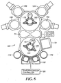
- Figure 5A shows a patterned dielectric having a barrier layer 54 formed thereon similar to that shown in Figure 2B.
- a cross-sectional diagram of the dual damascene via and wire definition having the conformal barrier layer 54 includes a conformal CVD Cu layer 102 which is uniformly deposited on field regions 56 and sidewalls 58 until the via is partially filled leaving a hole 104.
- the CVD Cu layer is then annealed by heating the wafer to a temperature from about 300°C to about 450°C to reflow the copper into the hole 104 and form a copper plug 106.
- a second conformal CVD Cu layer 108 is then uniformly deposited on the annealed CVD layer until the trenches are partially filled leaving a hole 110.
- the second CVD Cu layer 108 us then annealed by heating the wafer to a temperature from abut 300°C to about 450°C to reflow the copper into the trench hole 110 and form a copper wire 112.
- the copper wires 112 are completed by planarization as previously described.
- FIG. 6 a schematic diagram of an integrated processing system 160 having both PVD and CVD chambers thereon in which the above described integrated processes can be implemented is shown.
- substrates are introduced and withdrawn from the processing system 160 through a cassette loadlock 162.
- a robot 164 having a blade 167 is located within the processing system 160 to move the substrates through the system 160.
- One robot 164 is typically positioned in a buffer chamber 168 to transfer substrates between the cassette loadlock 162, degas wafer orientation chamber 170, preclean chamber 172, PVD TiN chamber 174 and cooldown chamber 176.
- a second robot 178 is located in transfer chamber 180 to transfer substrates to and from the cooldown chamber 176, coherent Ti chamber 182, CVD Tin chamber 184, CVD Cu chamber 186 and PVD IMP Cu processing chamber 188.
- the transfer chamber 180 in the integrated system is preferably maintained at low pressure or high vacuum in the range 10 -3 to 10 -8 torr.
- This specific configuration of the chambers in Figure 6 comprise an integrated processing system capable of both CVD and PVD processes in a single cluster tool.
- This particular chamber configuration or arrangement is merely illustrative and more configurations of PVD and CVD processes are contemplated by the present invention.
- a substrate processed in the processing system 160 is passed from the cassette loadlock 162 to the buffer chamber 168 where the robot 164 first moves the substrate into a degas chamber 170. The substrate is then be transferred into preclean chamber 172, PVD TiN chamber 174, and then into a cooldown chamber 176. From the cooldown chamber 176, the robot 178 typically moves the substrate into and between one or more processing chambers before returning the substrate back to the cooldown chamber 176. It is anticipated that the substrate may be processed or cooled in one or more chambers any number of times in any order to accomplish fabrication of a desired structure on the substrate. The substrate is removed from the processing system 160, following processing, through the buffer chamber 168 and then to the loadlock 162. A microprocessor controller 190 controls the sequence and formation of the layers on the substrates.
- the processing system 160 passes a substrate through loadlock 162 into de-gas chamber 170 wherein the substrate is introduced to outgas contaminants.
- a substrate is then moved into a pre-clean chamber 172 where the surface of the substrate is cleaned to remove any contaminants thereon.
- the substrate is then processed in a CVD-TiN chamber 175 to deposit a barrier layer on the dielectric layer.
- the robot 178 then transfers the substrate to a CVD Cu 174.
- the substrate receives two or more layers of the metal to form the metal plug and interconnect. Annealing can occur in any heated chamber. After the metal layer is fully deposited, the substrate is sent to a planarization unit.
- a staged-vacuum wafer processing system is disclosed in United States Patent No. 5,186,718, entitled “Staged-Vacuum Wafer Processing System and Method,” Tepman et al., issued on February 16, 1993. This system has been modified to accommodate a CVD chamber thereon.
- a CVD Cu layer may be deposited using by any known CVD Cu process or precursor gas, including copper +2 (hfac) 2 and Cu +2 (fod) 2 (fod being an abbreviation for heptafluoro dimethyl octanediene), but a preferred process uses the volatile liquid complex copper+1hfac, TMVS (hfac being an abbreviation for the hexafluoro acetylacetonate anion and TMVS being an abbreviation for trimethylvinylsilane) with argon as the carrier gas. Because this complex is a liquid under ambient conditions, it can be utilized in standard CVD bubbler precursor delivery systems currently used in semiconductor fabrication.
- Both TMVS and copper +2 (hfac) 2 are volatile byproducts of the deposition reaction that are exhausted from the chamber.
- the deposition reaction is believed to proceed according to the following mechanism, in which (s) denoted interaction with a surface and (g) denotes the gas phase.
- 2Cu+1hfac, TMVS(g) ----- 2Cu+1hfac, TMVS(s) step (1) 2Cu +1 hfac,TMVS(s) ----- 2Cu +1 hfac(s) + 2TMVS(g) step (2) 2Cu +1 hfac(s) ----- Cu(s) + Cu +2 (hfac) 2 (g) step (3)
- step 1 the complex is adsorbed from the gas phase onto a metallic surface.
- step 2 the coordinated olefin (TMVS in this specific case) dissociates from the complex as a free gas leaving behind Cu +1 hfac as an unstable compound.
- step 3 the Cu +1 hfac disassociates to yield copper metal and volatile Cu +2 (hfac) 2 .
- the disassociation at CVD temperatures appears to be most strongly catalyzed by metallic or electrically conducting surfaces.
- the organometallic copper complex can be reduced by hydrogen to yield metallic copper.
- the volatile liquid complex, Cu +1 hfac,TMVS can be used to deposit Cu through either a thermal or plasma based process, with the thermal based process being most preferred.
- the substrate temperature for the plasma enhanced process is preferably between about 100 and about 400°C, while that for the thermal process is between about 50 and about 300°C, most preferably about 170°C.
- a CVD Cu wetting layer may be provided over a nucleation layer.
- electroplated copper may be used in combination with or in replacement of the CVD Cu wetting layer.
- the substrate is then sent to a PVD Cu chamber to deposit PVD Cu below the melting point temperature of the CVD Cu and PVD Cu.
- the soft metal is copper
- the PVD Cu be deposited at a wafer temperature below about 550°C, preferably below about 400°C.
- the copper layers start to flow during the PVD deposition process at above 200°C, with the tantalum barrier/wetting layer remaining firmly in place as a solid metal layer. Because tantalum has good wetting with copper, the CVD Cu is prevented from dewetting the tantalum at about 400°C and, therefore, wafer temperatures above the melting point of aluminum (>660°C), as taught by the prior art CVD process, are not required. Therefore, the application of a thin tantalum layer enables planarization of the copper to be achieved at temperatures far below the melting point of the copper.
- deposited Cu layers may be annealed with H 2 to make the layer more resistant to formation of CuO.
- Copper electroplating is much less costly than PVD or CVD processes, but can not be performed in the integrated processing system. Fortunately, exposure of the substrate to air when transferring between different process equipment has not formed a noticeable interface in the metal layer.
Landscapes
- Engineering & Computer Science (AREA)
- Physics & Mathematics (AREA)
- Condensed Matter Physics & Semiconductors (AREA)
- General Physics & Mathematics (AREA)
- Manufacturing & Machinery (AREA)
- Computer Hardware Design (AREA)
- Microelectronics & Electronic Packaging (AREA)
- Power Engineering (AREA)
- Plasma & Fusion (AREA)
- Internal Circuitry In Semiconductor Integrated Circuit Devices (AREA)
Claims (8)
- Procédé de formation d'une interconnexion à double damasquinage dans une couche de diélectrique présentant une définition de traversées et de câbles à double damasquinage, comprenant les étapes consistant à :a) déposer une couche barrière sur les surfaces exposées de la couche de diélectrique,b) procéder à un dépôt chimique en phase vapeur ou à une électrodéposition d'un métal conducteur sur la couche barrière,c) recuire le métal conducteur pour remplir la définition de traversées après le dépôt chimique en phase vapeur ou l'électrodéposition,d) procéder à un dépôt physique en phase vapeur du métal conducteur pour remplir la définition de câbles après le recuit, ete) aplanir le métal conducteur, la couche barrière et la couche de diélectrique pour définir un câble conducteur.
- Procédé selon la revendication 1, dans lequel le métal conducteur est sélectionné dans le groupe constitué de cuivre, d'aluminium, de cuivre dopé, d'aluminium dopé, et de leurs mélanges.
- Procédé selon la revendication 1, dans lequel les étapes a) et b) sont exécutées dans un système de traitement intégré.
- Procédé selon la revendication 1, dans lequel l'étape consistant à aplanir est exécutée par le biais d'un polissage chimique-mécanique.
- Procédé selon la revendication 1, dans lequel la couche barrière comprend un matériau sélectionné dans le groupe constitué de titane, de nitrure de titane, de nitrure de silicium de titane, de nitrure de tungstène, de nitrure de silicium de tungstène, de tantale, de nitrure de tantale, de nitrure de silicium de tantale, de silicium dopé, d'aluminium, et d'oxydes d'aluminium.
- Procédé selon la revendication 1, dans lequel le métal conducteur est du cuivre ou du cuivre dopé.
- Procédé selon la revendication 1, dans lequel l'étape b) comprend un dépôt chimique en phase vapeur.
- Procédé selon la revendication 1, dans lequel l'étape b) comprend une électrodéposition.
Applications Claiming Priority (3)
| Application Number | Priority Date | Filing Date | Title |
|---|---|---|---|
| US914521 | 1997-08-19 | ||
| US08/914,521 US5989623A (en) | 1997-08-19 | 1997-08-19 | Dual damascene metallization |
| PCT/US1998/017010 WO1999009593A1 (fr) | 1997-08-19 | 1998-08-17 | Metallisation a double damasquinage |
Publications (2)
| Publication Number | Publication Date |
|---|---|
| EP1021827A1 EP1021827A1 (fr) | 2000-07-26 |
| EP1021827B1 true EP1021827B1 (fr) | 2007-04-25 |
Family
ID=25434472
Family Applications (1)
| Application Number | Title | Priority Date | Filing Date |
|---|---|---|---|
| EP98939967A Expired - Lifetime EP1021827B1 (fr) | 1997-08-19 | 1998-08-17 | Metallisation a double damasquinage |
Country Status (6)
| Country | Link |
|---|---|
| US (2) | US5989623A (fr) |
| EP (1) | EP1021827B1 (fr) |
| JP (1) | JP4615707B2 (fr) |
| KR (1) | KR100506139B1 (fr) |
| DE (1) | DE69837674T2 (fr) |
| WO (1) | WO1999009593A1 (fr) |
Cited By (1)
| Publication number | Priority date | Publication date | Assignee | Title |
|---|---|---|---|---|
| CN102332425A (zh) * | 2011-09-23 | 2012-01-25 | 复旦大学 | 一种提升铜互连技术中抗电迁移特性的方法 |
Families Citing this family (122)
| Publication number | Priority date | Publication date | Assignee | Title |
|---|---|---|---|---|
| US6475903B1 (en) * | 1993-12-28 | 2002-11-05 | Intel Corporation | Copper reflow process |
| US6100196A (en) * | 1996-04-08 | 2000-08-08 | Chartered Semiconductor Manufacturing Ltd. | Method of making a copper interconnect with top barrier layer |
| US6429120B1 (en) * | 2000-01-18 | 2002-08-06 | Micron Technology, Inc. | Methods and apparatus for making integrated-circuit wiring from copper, silver, gold, and other metals |
| US6731007B1 (en) * | 1997-08-29 | 2004-05-04 | Hitachi, Ltd. | Semiconductor integrated circuit device with vertically stacked conductor interconnections |
| US6307267B1 (en) * | 1997-12-26 | 2001-10-23 | Kabushiki Kaisha Toshiba | Semiconductor device and manufacturing method thereof |
| US6140234A (en) * | 1998-01-20 | 2000-10-31 | International Business Machines Corporation | Method to selectively fill recesses with conductive metal |
| EP1019954B1 (fr) | 1998-02-04 | 2013-05-15 | Applied Materials, Inc. | Procédé et appareil de recuit a basse temperature intervenant après dépot électrolytique de microstructures de cuivre destinées à un dispositif micro-electronique |
| US7244677B2 (en) | 1998-02-04 | 2007-07-17 | Semitool. Inc. | Method for filling recessed micro-structures with metallization in the production of a microelectronic device |
| US6025264A (en) * | 1998-02-09 | 2000-02-15 | United Microelectronics Corp. | Fabricating method of a barrier layer |
| US6682970B1 (en) * | 1998-02-27 | 2004-01-27 | Micron Technology, Inc. | Capacitor/antifuse structure having a barrier-layer electrode and improved barrier layer |
| US6150706A (en) | 1998-02-27 | 2000-11-21 | Micron Technology, Inc. | Capacitor/antifuse structure having a barrier-layer electrode and improved barrier layer |
| US7034353B2 (en) * | 1998-02-27 | 2006-04-25 | Micron Technology, Inc. | Methods for enhancing capacitors having roughened features to increase charge-storage capacity |
| JP3149846B2 (ja) * | 1998-04-17 | 2001-03-26 | 日本電気株式会社 | 半導体装置及びその製造方法 |
| US6517894B1 (en) * | 1998-04-30 | 2003-02-11 | Ebara Corporation | Method for plating a first layer on a substrate and a second layer on the first layer |
| US6433428B1 (en) * | 1998-05-29 | 2002-08-13 | Kabushiki Kaisha Toshiba | Semiconductor device with a dual damascene type via contact structure and method for the manufacture of same |
| US6475912B1 (en) | 1998-06-01 | 2002-11-05 | Matsushita Electric Industrial Co., Ltd. | Semiconductor device and method and apparatus for fabricating the same while minimizing operating failures and optimizing yield |
| US6355562B1 (en) | 1998-07-01 | 2002-03-12 | Advanced Technology Materials, Inc. | Adhesion promotion method for CVD copper metallization in IC applications |
| KR100265772B1 (ko) * | 1998-07-22 | 2000-10-02 | 윤종용 | 반도체 장치의 배선구조 및 그 제조방법 |
| JP3244058B2 (ja) * | 1998-07-28 | 2002-01-07 | 日本電気株式会社 | 半導体装置の製造方法 |
| US6093623A (en) * | 1998-08-04 | 2000-07-25 | Micron Technology, Inc. | Methods for making silicon-on-insulator structures |
| US6284656B1 (en) | 1998-08-04 | 2001-09-04 | Micron Technology, Inc. | Copper metallurgy in integrated circuits |
| JP2000068230A (ja) * | 1998-08-25 | 2000-03-03 | Mitsubishi Electric Corp | 半導体装置、その製造装置、および、その製造方法 |
| US6380083B1 (en) | 1998-08-28 | 2002-04-30 | Agere Systems Guardian Corp. | Process for semiconductor device fabrication having copper interconnects |
| JP3187011B2 (ja) * | 1998-08-31 | 2001-07-11 | 日本電気株式会社 | 半導体装置の製造方法 |
| US6288442B1 (en) * | 1998-09-10 | 2001-09-11 | Micron Technology, Inc. | Integrated circuit with oxidation-resistant polymeric layer |
| US5994778A (en) * | 1998-09-18 | 1999-11-30 | Advanced Micro Devices, Inc. | Surface treatment of low-k SiOF to prevent metal interaction |
| JP3180779B2 (ja) * | 1998-10-05 | 2001-06-25 | 日本電気株式会社 | 半導体装置の製造方法 |
| US6153528A (en) * | 1998-10-14 | 2000-11-28 | United Silicon Incorporated | Method of fabricating a dual damascene structure |
| US6080663A (en) * | 1998-11-13 | 2000-06-27 | United Microelectronics Corp. | Dual damascene |
| US6184137B1 (en) | 1998-11-25 | 2001-02-06 | Applied Materials, Inc. | Structure and method for improving low temperature copper reflow in semiconductor features |
| US6207568B1 (en) * | 1998-11-27 | 2001-03-27 | Taiwan Semiconductor Manufacturing Company | Ionized metal plasma (IMP) method for forming (111) oriented aluminum containing conductor layer |
| US6596637B1 (en) * | 1998-12-07 | 2003-07-22 | Advanced Micro Devices, Inc. | Chemically preventing Cu dendrite formation and growth by immersion |
| US6162728A (en) * | 1998-12-18 | 2000-12-19 | Texas Instruments Incorporated | Method to optimize copper chemical-mechanical polishing in a copper damascene interconnect process for integrated circuit applications |
| US6288449B1 (en) * | 1998-12-22 | 2001-09-11 | Agere Systems Guardian Corp. | Barrier for copper metallization |
| KR100280288B1 (ko) | 1999-02-04 | 2001-01-15 | 윤종용 | 반도체 집적회로의 커패시터 제조방법 |
| SG90054A1 (en) * | 1999-02-11 | 2002-07-23 | Chartered Semiconductor Mfg | A new process of dual damascene structure |
| US20020127845A1 (en) * | 1999-03-01 | 2002-09-12 | Paul A. Farrar | Conductive structures in integrated circuits |
| KR100460746B1 (ko) * | 1999-04-13 | 2004-12-09 | 주식회사 하이닉스반도체 | 반도체 소자의 구리 금속 배선 형성 방법 |
| US6103624A (en) * | 1999-04-15 | 2000-08-15 | Advanced Micro Devices, Inc. | Method of improving Cu damascene interconnect reliability by laser anneal before barrier polish |
| US6303496B1 (en) * | 1999-04-27 | 2001-10-16 | Cypress Semiconductor Corporation | Methods of filling constrained spaces with insulating materials and/or of forming contact holes and/or contacts in an integrated circuit |
| US6251772B1 (en) * | 1999-04-29 | 2001-06-26 | Advanced Micro Devicees, Inc. | Dielectric adhesion enhancement in damascene process for semiconductors |
| KR100333712B1 (ko) * | 1999-06-24 | 2002-04-24 | 박종섭 | 반도체 소자의 상감형 금속배선 형성방법 |
| US6251770B1 (en) | 1999-06-30 | 2001-06-26 | Lam Research Corp. | Dual-damascene dielectric structures and methods for making the same |
| US20040034134A1 (en) * | 1999-08-26 | 2004-02-19 | Lamb James E. | Crosslinkable fill compositions for uniformly protecting via and contact holes |
| CN1196180C (zh) | 1999-08-26 | 2005-04-06 | 部鲁尔科学公司 | 改进的用于双金属镶嵌方法中的填充物料 |
| US6326297B1 (en) * | 1999-09-30 | 2001-12-04 | Novellus Systems, Inc. | Method of making a tungsten nitride barrier layer with improved adhesion and stability using a silicon layer |
| US6423200B1 (en) * | 1999-09-30 | 2002-07-23 | Lam Research Corporation | Copper interconnect seed layer treatment methods and apparatuses for treating the same |
| EP1221177B1 (fr) * | 1999-10-15 | 2006-05-31 | Asm International N.V. | Couches de garnissage, a caracteristiques uniformes, destinees a une metallisation de damasquinage |
| US6361880B1 (en) * | 1999-12-22 | 2002-03-26 | International Business Machines Corporation | CVD/PVD/CVD/PVD fill process |
| KR100338112B1 (ko) * | 1999-12-22 | 2002-05-24 | 박종섭 | 반도체 소자의 구리 금속 배선 형성 방법 |
| US7262130B1 (en) * | 2000-01-18 | 2007-08-28 | Micron Technology, Inc. | Methods for making integrated-circuit wiring from copper, silver, gold, and other metals |
| US6376370B1 (en) | 2000-01-18 | 2002-04-23 | Micron Technology, Inc. | Process for providing seed layers for using aluminum, copper, gold and silver metallurgy process for providing seed layers for using aluminum, copper, gold and silver metallurgy |
| US6420262B1 (en) | 2000-01-18 | 2002-07-16 | Micron Technology, Inc. | Structures and methods to enhance copper metallization |
| US7211512B1 (en) * | 2000-01-18 | 2007-05-01 | Micron Technology, Inc. | Selective electroless-plated copper metallization |
| US6355555B1 (en) | 2000-01-28 | 2002-03-12 | Advanced Micro Devices, Inc. | Method of fabricating copper-based semiconductor devices using a sacrificial dielectric layer |
| US6303486B1 (en) | 2000-01-28 | 2001-10-16 | Advanced Micro Devices, Inc. | Method of fabricating copper-based semiconductor devices using a sacrificial dielectric layer and an unconstrained copper anneal |
| US6573030B1 (en) | 2000-02-17 | 2003-06-03 | Applied Materials, Inc. | Method for depositing an amorphous carbon layer |
| DE10008572B4 (de) * | 2000-02-24 | 2007-08-09 | Infineon Technologies Ag | Verbindungseinrichtung für Leistungshalbleitermodule |
| US6384448B1 (en) | 2000-02-28 | 2002-05-07 | Micron Technology, Inc. | P-channel dynamic flash memory cells with ultrathin tunnel oxides |
| US6639835B2 (en) | 2000-02-29 | 2003-10-28 | Micron Technology, Inc. | Static NVRAM with ultra thin tunnel oxides |
| US6486063B2 (en) * | 2000-03-02 | 2002-11-26 | Tokyo Electron Limited | Semiconductor device manufacturing method for a copper connection |
| US6344125B1 (en) * | 2000-04-06 | 2002-02-05 | International Business Machines Corporation | Pattern-sensitive electrolytic metal plating |
| US6674167B1 (en) * | 2000-05-31 | 2004-01-06 | Micron Technology, Inc. | Multilevel copper interconnect with double passivation |
| US6423629B1 (en) * | 2000-05-31 | 2002-07-23 | Kie Y. Ahn | Multilevel copper interconnects with low-k dielectrics and air gaps |
| US6258709B1 (en) | 2000-06-07 | 2001-07-10 | Micron Technology, Inc. | Formation of electrical interconnect lines by selective metal etch |
| US6346479B1 (en) | 2000-06-14 | 2002-02-12 | Advanced Micro Devices, Inc. | Method of manufacturing a semiconductor device having copper interconnects |
| US6525425B1 (en) * | 2000-06-14 | 2003-02-25 | Advanced Micro Devices, Inc. | Copper interconnects with improved electromigration resistance and low resistivity |
| US6548395B1 (en) * | 2000-11-16 | 2003-04-15 | Advanced Micro Devices, Inc. | Method of promoting void free copper interconnects |
| US6776893B1 (en) | 2000-11-20 | 2004-08-17 | Enthone Inc. | Electroplating chemistry for the CU filling of submicron features of VLSI/ULSI interconnect |
| US7270724B2 (en) | 2000-12-13 | 2007-09-18 | Uvtech Systems, Inc. | Scanning plasma reactor |
| KR100364260B1 (ko) * | 2001-01-05 | 2002-12-11 | 삼성전자 주식회사 | 반도체 집적 회로의 제조 방법 |
| US6773683B2 (en) | 2001-01-08 | 2004-08-10 | Uvtech Systems, Inc. | Photocatalytic reactor system for treating flue effluents |
| US6383920B1 (en) | 2001-01-10 | 2002-05-07 | International Business Machines Corporation | Process of enclosing via for improved reliability in dual damascene interconnects |
| KR100379551B1 (ko) * | 2001-03-09 | 2003-04-10 | 주식회사 하이닉스반도체 | 듀얼 다마신 공정을 이용한 반도체 소자의 제조방법 |
| US7224063B2 (en) | 2001-06-01 | 2007-05-29 | International Business Machines Corporation | Dual-damascene metallization interconnection |
| US20020192944A1 (en) * | 2001-06-13 | 2002-12-19 | Sonderman Thomas J. | Method and apparatus for controlling a thickness of a copper film |
| US6849545B2 (en) * | 2001-06-20 | 2005-02-01 | Applied Materials, Inc. | System and method to form a composite film stack utilizing sequential deposition techniques |
| US20030008243A1 (en) * | 2001-07-09 | 2003-01-09 | Micron Technology, Inc. | Copper electroless deposition technology for ULSI metalization |
| US6692830B2 (en) * | 2001-07-31 | 2004-02-17 | Flex Products, Inc. | Diffractive pigment flakes and compositions |
| US6607976B2 (en) | 2001-09-25 | 2003-08-19 | Applied Materials, Inc. | Copper interconnect barrier layer structure and formation method |
| US6873027B2 (en) | 2001-10-26 | 2005-03-29 | International Business Machines Corporation | Encapsulated energy-dissipative fuse for integrated circuits and method of making the same |
| KR100453957B1 (ko) * | 2001-12-20 | 2004-10-20 | 동부전자 주식회사 | 듀얼 다마신을 이용한 전원 배선 제조 방법 |
| US6620635B2 (en) * | 2002-02-20 | 2003-09-16 | International Business Machines Corporation | Damascene resistor and method for measuring the width of same |
| US6624515B1 (en) * | 2002-03-11 | 2003-09-23 | Micron Technology, Inc. | Microelectronic die including low RC under-layer interconnects |
| US6541397B1 (en) | 2002-03-29 | 2003-04-01 | Applied Materials, Inc. | Removable amorphous carbon CMP stop |
| US6518185B1 (en) * | 2002-04-22 | 2003-02-11 | Advanced Micro Devices, Inc. | Integration scheme for non-feature-size dependent cu-alloy introduction |
| US6656840B2 (en) | 2002-04-29 | 2003-12-02 | Applied Materials Inc. | Method for forming silicon containing layers on a substrate |
| US6620724B1 (en) * | 2002-05-09 | 2003-09-16 | Infineon Technologies Ag | Low resistivity deep trench fill for DRAM and EDRAM applications |
| US6649513B1 (en) | 2002-05-15 | 2003-11-18 | Taiwan Semiconductor Manufacturing Company | Copper back-end-of-line by electropolish |
| KR100456259B1 (ko) * | 2002-07-15 | 2004-11-09 | 주식회사 하이닉스반도체 | 반도체 소자의 구리 배선 형성방법 |
| US6784049B2 (en) * | 2002-08-28 | 2004-08-31 | Micron Technology, Inc. | Method for forming refractory metal oxide layers with tetramethyldisiloxane |
| US7030042B2 (en) * | 2002-08-28 | 2006-04-18 | Micron Technology, Inc. | Systems and methods for forming tantalum oxide layers and tantalum precursor compounds |
| US6709970B1 (en) * | 2002-09-03 | 2004-03-23 | Samsung Electronics Co., Ltd. | Method for creating a damascene interconnect using a two-step electroplating process |
| US6919639B2 (en) * | 2002-10-15 | 2005-07-19 | The Board Of Regents, The University Of Texas System | Multiple copper vias for integrated circuit metallization and methods of fabricating same |
| US6980395B2 (en) * | 2002-10-31 | 2005-12-27 | International Business Machines Corporation | Enhanced coplanar conductance structure for inductive heads |
| US20040108217A1 (en) * | 2002-12-05 | 2004-06-10 | Dubin Valery M. | Methods for forming copper interconnect structures by co-plating of noble metals and structures formed thereby |
| US7273808B1 (en) | 2003-02-03 | 2007-09-25 | Novellus Systems, Inc. | Reactive barrier/seed preclean process for damascene process |
| KR100576363B1 (ko) * | 2003-05-30 | 2006-05-03 | 삼성전자주식회사 | 인시투 화학기상증착 금속 공정 및 그에 사용되는화학기상증착 장비 |
| JP2005039142A (ja) * | 2003-07-18 | 2005-02-10 | Nec Electronics Corp | 半導体装置の製造方法 |
| US7220665B2 (en) | 2003-08-05 | 2007-05-22 | Micron Technology, Inc. | H2 plasma treatment |
| US7026244B2 (en) * | 2003-08-08 | 2006-04-11 | Taiwan Semiconductor Manufacturing Co., Ltd. | Low resistance and reliable copper interconnects by variable doping |
| US7064068B2 (en) * | 2004-01-23 | 2006-06-20 | Taiwan Semiconductor Manufacturing Company, Ltd. | Method to improve planarity of electroplated copper |
| KR100613283B1 (ko) | 2004-12-27 | 2006-08-21 | 동부일렉트로닉스 주식회사 | 반도체 소자의 배선 형성방법 |
| CN1983550A (zh) * | 2005-12-14 | 2007-06-20 | 中芯国际集成电路制造(上海)有限公司 | 提高可靠性和成品率的消除铜位错的方法 |
| US20070281456A1 (en) * | 2006-05-30 | 2007-12-06 | Hynix Semiconductor Inc. | Method of forming line of semiconductor device |
| KR100750950B1 (ko) * | 2006-07-18 | 2007-08-22 | 삼성전자주식회사 | 반도체 장치의 배선 구조물 및 그 형성 방법, 비휘발성메모리 장치 및 그 제조 방법 |
| WO2008084524A1 (fr) * | 2007-01-09 | 2008-07-17 | Fujitsu Microelectronics Limited | Procédé et appareil de production de dispositif à semi-conducteur |
| KR20090053991A (ko) * | 2007-11-26 | 2009-05-29 | 주식회사 동부하이텍 | 반도체 소자의 제조방법 |
| US20090168247A1 (en) * | 2007-12-28 | 2009-07-02 | Christian Rene Bonhote | Magnetic head with embedded solder connection and method for manufacture thereof |
| US8252653B2 (en) * | 2008-10-21 | 2012-08-28 | Applied Materials, Inc. | Method of forming a non-volatile memory having a silicon nitride charge trap layer |
| US8198671B2 (en) * | 2009-04-22 | 2012-06-12 | Applied Materials, Inc. | Modification of charge trap silicon nitride with oxygen plasma |
| US8575000B2 (en) * | 2011-07-19 | 2013-11-05 | SanDisk Technologies, Inc. | Copper interconnects separated by air gaps and method of making thereof |
| US8796853B2 (en) * | 2012-02-24 | 2014-08-05 | International Business Machines Corporation | Metallic capped interconnect structure with high electromigration resistance and low resistivity |
| US8802558B2 (en) | 2012-11-07 | 2014-08-12 | International Business Machines Corporation | Copper interconnect structures and methods of making same |
| US8999767B2 (en) * | 2013-01-31 | 2015-04-07 | International Business Machines Corporation | Electronic fuse having an insulation layer |
| US9425092B2 (en) | 2013-03-15 | 2016-08-23 | Applied Materials, Inc. | Methods for producing interconnects in semiconductor devices |
| JP6385856B2 (ja) * | 2015-02-26 | 2018-09-05 | 東京エレクトロン株式会社 | Cu配線の形成方法および半導体装置の製造方法 |
| US20160276156A1 (en) * | 2015-03-16 | 2016-09-22 | Taiwan Semiconductor Manufacturing Company Ltd. | Semiconductor device and manufacturing process thereof |
| US9704804B1 (en) * | 2015-12-18 | 2017-07-11 | Texas Instruments Incorporated | Oxidation resistant barrier metal process for semiconductor devices |
| US11664271B2 (en) | 2019-05-02 | 2023-05-30 | International Business Machines Corporation | Dual damascene with short liner |
| CN112825307B (zh) * | 2019-11-21 | 2022-04-29 | 中芯国际集成电路制造(上海)有限公司 | 一种互连结构的形成方法及互连结构 |
| CN113363204B (zh) * | 2020-03-05 | 2022-04-12 | 中芯国际集成电路制造(深圳)有限公司 | 一种互连结构的形成方法 |
Family Cites Families (41)
| Publication number | Priority date | Publication date | Assignee | Title |
|---|---|---|---|---|
| US5010032A (en) * | 1985-05-01 | 1991-04-23 | Texas Instruments Incorporated | Process for making CMOS device with both P+ and N+ gates including refractory metal silicide and nitride interconnects |
| JPS639925A (ja) * | 1986-06-30 | 1988-01-16 | Nec Corp | 半導体装置の製造方法 |
| JPS6373660A (ja) * | 1986-09-17 | 1988-04-04 | Fujitsu Ltd | 半導体装置 |
| US4960732A (en) * | 1987-02-19 | 1990-10-02 | Advanced Micro Devices, Inc. | Contact plug and interconnect employing a barrier lining and a backfilled conductor material |
| JPS63229814A (ja) * | 1987-03-19 | 1988-09-26 | Nec Corp | 半導体集積回路の製造方法 |
| US4994410A (en) * | 1988-04-04 | 1991-02-19 | Motorola, Inc. | Method for device metallization by forming a contact plug and interconnect using a silicide/nitride process |
| US4938996A (en) * | 1988-04-12 | 1990-07-03 | Ziv Alan R | Via filling by selective laser chemical vapor deposition |
| US4920072A (en) * | 1988-10-31 | 1990-04-24 | Texas Instruments Incorporated | Method of forming metal interconnects |
| US4920073A (en) * | 1989-05-11 | 1990-04-24 | Texas Instruments, Incorporated | Selective silicidation process using a titanium nitride protective layer |
| JPH038359A (ja) * | 1989-06-06 | 1991-01-16 | Fujitsu Ltd | 半導体装置の製造方法 |
| US5091339A (en) * | 1990-07-23 | 1992-02-25 | Microelectronics And Computer Technology Corporation | Trenching techniques for forming vias and channels in multilayer electrical interconnects |
| US5250465A (en) * | 1991-01-28 | 1993-10-05 | Fujitsu Limited | Method of manufacturing semiconductor devices |
| JP2533414B2 (ja) * | 1991-04-09 | 1996-09-11 | 三菱電機株式会社 | 半導体集積回路装置の配線接続構造およびその製造方法 |
| US5292558A (en) * | 1991-08-08 | 1994-03-08 | University Of Texas At Austin, Texas | Process for metal deposition for microelectronic interconnections |
| JPH05206064A (ja) * | 1991-12-10 | 1993-08-13 | Nec Corp | 半導体装置の製造方法 |
| US5300813A (en) * | 1992-02-26 | 1994-04-05 | International Business Machines Corporation | Refractory metal capped low resistivity metal conductor lines and vias |
| US5262354A (en) * | 1992-02-26 | 1993-11-16 | International Business Machines Corporation | Refractory metal capped low resistivity metal conductor lines and vias |
| US5739579A (en) * | 1992-06-29 | 1998-04-14 | Intel Corporation | Method for forming interconnections for semiconductor fabrication and semiconductor device having such interconnections |
| CA2082771C (fr) * | 1992-11-12 | 1998-02-10 | Vu Quoc Ho | Methode de faconnage des interconnexions pour circuits imprimes |
| US5439731A (en) * | 1994-03-11 | 1995-08-08 | Cornell Research Goundation, Inc. | Interconnect structures containing blocked segments to minimize stress migration and electromigration damage |
| KR0144956B1 (ko) * | 1994-06-10 | 1998-08-17 | 김광호 | 반도체 장치의 배선 구조 및 그 형성방법 |
| JPH0810693A (ja) * | 1994-06-30 | 1996-01-16 | Dainippon Screen Mfg Co Ltd | レジスト膜の乾燥方法及び装置 |
| US5521119A (en) * | 1994-07-13 | 1996-05-28 | Taiwan Semiconductor Manufacturing Co. | Post treatment of tungsten etching back |
| JPH08181141A (ja) * | 1994-12-21 | 1996-07-12 | Yamaha Corp | 配線形成法 |
| EP0720227B1 (fr) * | 1994-12-29 | 2004-12-01 | STMicroelectronics, Inc. | Structure de connexion électrique sur un dispositif de circuit intégré comprenant un bouchon à tête agrandie |
| KR100413890B1 (ko) * | 1995-03-02 | 2004-03-19 | 동경 엘렉트론 주식회사 | 반도체장치의제조방법및제조장치 |
| JP3266492B2 (ja) * | 1995-03-02 | 2002-03-18 | 川崎マイクロエレクトロニクス株式会社 | 半導体装置の製造方法 |
| JP2728025B2 (ja) * | 1995-04-13 | 1998-03-18 | 日本電気株式会社 | 半導体装置の製造方法 |
| US5877087A (en) * | 1995-11-21 | 1999-03-02 | Applied Materials, Inc. | Low temperature integrated metallization process and apparatus |
| US5824599A (en) * | 1996-01-16 | 1998-10-20 | Cornell Research Foundation, Inc. | Protected encapsulation of catalytic layer for electroless copper interconnect |
| US5895266A (en) * | 1996-02-26 | 1999-04-20 | Applied Materials, Inc. | Titanium nitride barrier layers |
| US5814557A (en) * | 1996-05-20 | 1998-09-29 | Motorola, Inc. | Method of forming an interconnect structure |
| US5693563A (en) * | 1996-07-15 | 1997-12-02 | Chartered Semiconductor Manufacturing Pte Ltd. | Etch stop for copper damascene process |
| JP3261317B2 (ja) * | 1996-08-30 | 2002-02-25 | 株式会社アルバック | 銅配線製造方法、及び銅配線 |
| JP3281816B2 (ja) * | 1996-09-02 | 2002-05-13 | 株式会社アルバック | 銅配線製造方法 |
| EP0932913A1 (fr) * | 1996-12-16 | 1999-08-04 | International Business Machines Corporation | Structures d'interconnexion plaquees sur microplaquettes de circuits integres |
| US5933753A (en) * | 1996-12-16 | 1999-08-03 | International Business Machines Corporation | Open-bottomed via liner structure and method for fabricating same |
| KR100243272B1 (ko) * | 1996-12-20 | 2000-03-02 | 윤종용 | 반도체 소자의 콘택 플러그 형성방법 |
| US5858873A (en) * | 1997-03-12 | 1999-01-12 | Lucent Technologies Inc. | Integrated circuit having amorphous silicide layer in contacts and vias and method of manufacture thereof |
| US5930669A (en) * | 1997-04-03 | 1999-07-27 | International Business Machines Corporation | Continuous highly conductive metal wiring structures and method for fabricating the same |
| JP3390329B2 (ja) * | 1997-06-27 | 2003-03-24 | 日本電気株式会社 | 半導体装置およびその製造方法 |
-
1997
- 1997-08-19 US US08/914,521 patent/US5989623A/en not_active Expired - Lifetime
-
1998
- 1998-08-17 KR KR10-2000-7001672A patent/KR100506139B1/ko not_active IP Right Cessation
- 1998-08-17 EP EP98939967A patent/EP1021827B1/fr not_active Expired - Lifetime
- 1998-08-17 JP JP2000510165A patent/JP4615707B2/ja not_active Expired - Fee Related
- 1998-08-17 DE DE69837674T patent/DE69837674T2/de not_active Expired - Fee Related
- 1998-08-17 WO PCT/US1998/017010 patent/WO1999009593A1/fr active IP Right Grant
-
1999
- 1999-08-24 US US09/379,696 patent/US6207222B1/en not_active Expired - Fee Related
Cited By (1)
| Publication number | Priority date | Publication date | Assignee | Title |
|---|---|---|---|---|
| CN102332425A (zh) * | 2011-09-23 | 2012-01-25 | 复旦大学 | 一种提升铜互连技术中抗电迁移特性的方法 |
Also Published As
| Publication number | Publication date |
|---|---|
| DE69837674D1 (de) | 2007-06-06 |
| JP4615707B2 (ja) | 2011-01-19 |
| DE69837674T2 (de) | 2008-01-10 |
| US6207222B1 (en) | 2001-03-27 |
| JP2001516146A (ja) | 2001-09-25 |
| KR100506139B1 (ko) | 2005-08-05 |
| EP1021827A1 (fr) | 2000-07-26 |
| WO1999009593A1 (fr) | 1999-02-25 |
| KR20010023055A (ko) | 2001-03-26 |
| US5989623A (en) | 1999-11-23 |
Similar Documents
| Publication | Publication Date | Title |
|---|---|---|
| EP1021827B1 (fr) | Metallisation a double damasquinage | |
| US7112528B2 (en) | Fully planarized dual damascene metallization using copper line interconnect and selective CVD aluminum plug | |
| US6458684B1 (en) | Single step process for blanket-selective CVD aluminum deposition | |
| US7550386B2 (en) | Advanced seed layers for interconnects | |
| US6924226B2 (en) | Methods for making multiple seed layers for metallic interconnects | |
| US8586471B2 (en) | Seed layers for metallic interconnects and products | |
| US7470612B2 (en) | Method of forming metal wiring layer of semiconductor device | |
| KR100339179B1 (ko) | 상호 접속 구조 및 그 형성 방법 | |
| US5250467A (en) | Method for forming low resistance and low defect density tungsten contacts to silicon semiconductor wafer | |
| US6120844A (en) | Deposition film orientation and reflectivity improvement using a self-aligning ultra-thin layer | |
| US6066358A (en) | Blanket-selective chemical vapor deposition using an ultra-thin nucleation layer | |
| US6110828A (en) | In-situ capped aluminum plug (CAP) process using selective CVD AL for integrated plug/interconnect metallization | |
| US5960320A (en) | Metal wiring layer forming method for semiconductor device | |
| JP2001516146A5 (fr) | ||
| JP4169950B2 (ja) | 半導体装置の製造方法 |
Legal Events
| Date | Code | Title | Description |
|---|---|---|---|
| PUAI | Public reference made under article 153(3) epc to a published international application that has entered the european phase |
Free format text: ORIGINAL CODE: 0009012 |
|
| 17P | Request for examination filed |
Effective date: 20000223 |
|
| AK | Designated contracting states |
Kind code of ref document: A1 Designated state(s): BE DE GB NL |
|
| GRAP | Despatch of communication of intention to grant a patent |
Free format text: ORIGINAL CODE: EPIDOSNIGR1 |
|
| GRAS | Grant fee paid |
Free format text: ORIGINAL CODE: EPIDOSNIGR3 |
|
| GRAA | (expected) grant |
Free format text: ORIGINAL CODE: 0009210 |
|
| AK | Designated contracting states |
Kind code of ref document: B1 Designated state(s): BE DE GB NL |
|
| REG | Reference to a national code |
Ref country code: GB Ref legal event code: FG4D |
|
| REF | Corresponds to: |
Ref document number: 69837674 Country of ref document: DE Date of ref document: 20070606 Kind code of ref document: P |
|
| PG25 | Lapsed in a contracting state [announced via postgrant information from national office to epo] |
Ref country code: BE Free format text: LAPSE BECAUSE OF FAILURE TO SUBMIT A TRANSLATION OF THE DESCRIPTION OR TO PAY THE FEE WITHIN THE PRESCRIBED TIME-LIMIT Effective date: 20070425 |
|
| PGFP | Annual fee paid to national office [announced via postgrant information from national office to epo] |
Ref country code: DE Payment date: 20071030 Year of fee payment: 10 |
|
| PLBE | No opposition filed within time limit |
Free format text: ORIGINAL CODE: 0009261 |
|
| STAA | Information on the status of an ep patent application or granted ep patent |
Free format text: STATUS: NO OPPOSITION FILED WITHIN TIME LIMIT |
|
| 26N | No opposition filed |
Effective date: 20080128 |
|
| GBPC | Gb: european patent ceased through non-payment of renewal fee |
Effective date: 20070817 |
|
| PGFP | Annual fee paid to national office [announced via postgrant information from national office to epo] |
Ref country code: NL Payment date: 20080715 Year of fee payment: 11 |
|
| PG25 | Lapsed in a contracting state [announced via postgrant information from national office to epo] |
Ref country code: GB Free format text: LAPSE BECAUSE OF NON-PAYMENT OF DUE FEES Effective date: 20070817 |
|
| PG25 | Lapsed in a contracting state [announced via postgrant information from national office to epo] |
Ref country code: DE Free format text: LAPSE BECAUSE OF NON-PAYMENT OF DUE FEES Effective date: 20090303 |
|
| REG | Reference to a national code |
Ref country code: NL Ref legal event code: V1 Effective date: 20100301 |
|
| PG25 | Lapsed in a contracting state [announced via postgrant information from national office to epo] |
Ref country code: NL Free format text: LAPSE BECAUSE OF NON-PAYMENT OF DUE FEES Effective date: 20100301 |