EP1019911B1 - Apparatus and method for device timing compensation - Google Patents
Apparatus and method for device timing compensation Download PDFInfo
- Publication number
- EP1019911B1 EP1019911B1 EP98949806A EP98949806A EP1019911B1 EP 1019911 B1 EP1019911 B1 EP 1019911B1 EP 98949806 A EP98949806 A EP 98949806A EP 98949806 A EP98949806 A EP 98949806A EP 1019911 B1 EP1019911 B1 EP 1019911B1
- Authority
- EP
- European Patent Office
- Prior art keywords
- column
- timing
- memory
- delay
- row
- Prior art date
- Legal status (The legal status is an assumption and is not a legal conclusion. Google has not performed a legal analysis and makes no representation as to the accuracy of the status listed.)
- Revoked
Links
Images


Classifications
-
- G—PHYSICS
- G11—INFORMATION STORAGE
- G11C—STATIC STORES
- G11C7/00—Arrangements for writing information into, or reading information out from, a digital store
- G11C7/10—Input/output [I/O] data interface arrangements, e.g. I/O data control circuits, I/O data buffers
- G11C7/1072—Input/output [I/O] data interface arrangements, e.g. I/O data control circuits, I/O data buffers for memories with random access ports synchronised on clock signal pulse trains, e.g. synchronous memories, self timed memories
-
- G—PHYSICS
- G11—INFORMATION STORAGE
- G11C—STATIC STORES
- G11C7/00—Arrangements for writing information into, or reading information out from, a digital store
- G11C7/22—Read-write [R-W] timing or clocking circuits; Read-write [R-W] control signal generators or management
-
- G—PHYSICS
- G11—INFORMATION STORAGE
- G11C—STATIC STORES
- G11C7/00—Arrangements for writing information into, or reading information out from, a digital store
- G11C7/22—Read-write [R-W] timing or clocking circuits; Read-write [R-W] control signal generators or management
- G11C7/222—Clock generating, synchronizing or distributing circuits within memory device
Definitions
- This invention relates generally to digital electronic systems. More particularly, this invention relates to techniques for efficiently transferring information in digital electronic systems.
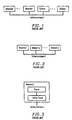
- a generalized multi-device digital electronic system there can be multiple master and slave devices which are connected by an interconnect structure, as shown in Figure 1. Wires between the components form the interconnect. Transport of information over the interconnect occurs from transmitter to receiver, where the master or the slave components can act as either transmitter or receiver.
- total delay to perform an operation is divided into clock cycles by dividing the entire datapath into separate pipe stages.
- total read latency is also divided into clock cycles.
- delay variations from both the interconnect and components are exposed. These delay variations can cause logical device-to-device conflicts which make the operation pipeline less efficient. It is thus desirable to compensate for these timing variations, which can occur depending on the position of the memory parts on the channel and internal delays in the memory devices.
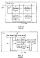
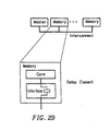
- Figure 3 illustrates a memory with a memory core and a memory interface.
- the memory interface interacts with an interconnect structure.
- the following discussion expands upon the generic memory elements of Figure 3 to identify separate structural elements and to discuss the memory operations and memory interactions with the interconnect.
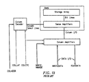
- a simple memory core typically consists of a storage array, column decoder, row decoder, and sense amplifiers, as shown in Figure 4.
- the interface 100 to a memory core generally consists of a row address 101, column address 103, and data path 102.
- the storage array, shown in Figure 6, is organized into rows and columns of storage cells, each of which stores one bit of information. Accessing the information in the storage array is a two step process. First, the information is transferred between the storage array and the sense amplifiers. Second, the information is transferred between the sense amplifiers and the interface via connection 100.
- the first major step, transferring information between the storage array and the sense amplifiers, is called a "row access" and is broken down into the minor steps of precharge and sense.
- the precharge step prepares the sense amplifiers and bit lines for sensing, typically by equilibrating them to a midpoint reference voltage.
- the row address is decoded, a single word line is asserted, the contents of the storage cell is placed on the bit lines, and the sense amplifier amplifies the value to a full rail state, completing the movement of the information from the storage array to the sense amplifiers.
- the sense amps can also serve as a local cache which stores a "page" of data which can be more quickly accessed with column read or write accesses.
- the second major step transferring information between the sense amplifiers and the interface, is called a "column access" and is typically performed in one step.
- this major step is broken up into two minor steps, e.g. putting a pipeline stage at the output of the column decoder. In this case the pipeline timing has to be adjusted.
- memory cores can also have multiple banks, which allow simultaneous row operations within a given core. Multiple banks improve memory performance through increased bank concurrency and reduced bank conflicts.
- Figure 5 shows a typical core structure with multiple banks. Each bank has its own storage array and can have its own set of sense amplifiers to allow for independent row operations. The column decoder and datapath are typically shared between banks.
- Figure 6 shows the generic storage array structure. As shown, the word line (106) accesses a row of storage cells, which in turn transfers the stored data on to the bit lines (107). While the figure shows a pair of bit lines connected to each storage cell, some core organizations may require only one bit line per cell, depending on the memory cell type and sensing circuits.
- the general memory core just described provides the basic framework for memory core structure and operations. However, there are a variety of core types, each with slight differences in structure and function. The following three subsections describe these differences for each major memory type.
- DRAM Dynamic RAM
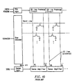
- FIG. 7 This section describes the structure and primitive operations for the conventional DRAM core.
- the structure of a conventional DRAM core is shown in Figure 7.
- the conventional DRAM structure has a row and column storage array organization and uses sense amplifiers to perform row access.
- the four primary memory operations, sense, precharge, read and write, are supported.
- the figure shows an additional "column amplifier” block, which is commonly used to speed column access.
- the core interface 100 consists of the following signals: row address 101, column address 103, data I/O bus 106, row control signals 107 (these signals are defined in detail further in this section), and column control signals 108 (these signals are defined in detail further in this section).
- Figure 8 shows a conventional DRAM core with multiple banks.
- the row decoder, column decoder, and column amplifiers are shared among the banks.
- Alternative organizations can allow for these elements to be replicated for each bank, but replication typically requires larger die area and thus greater cost.
- Cheap core designs with multiple banks typically share row decoders, column decoders and column datapaths between banks to minimize die area.
- DRAM cores use a single transistor (IT) cell.
- the single transistor accesses a data value stored on a capacitor, as shown in Figure 9.
- This simple storage cell achieves high storage density, and hence a low cost per bit, but has two detrimental side effects.
- the relatively slow access time arises because the passive storage capacitor can only store a limited amount of charge.
- Row sensing for conventional DRAM takes longer than for other memory types with actively-driven cells, such as SRAM.
- cheap DRAM cores generally result in slow row access and cycle times.
- Another problem is that cell refresh is required. Since the bit value is stored on a passive capacitor, the leakage current in the capacitor and access transistor result in degradation of the stored value.
- refresh sense and refresh precharge are two additional memory operations.
- refresh sense and refresh precharge were the same as regular sense and precharge operations.
- special refresh operations are advantageous to enable dedicated refresh circuits and logic to support multibank refresh.
- Figure 10 shows details of a bit slice of a typical row datapath
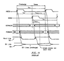
- Figure 11 shows the timing diagram of a precharge and sense operation.
- the bit lines and sense amplifiers must first be precharged, typically to the Vdd/2 midpoint.
- the row precharge time, tRP is shown in Figure 11.
- the row decoder drives a single word line to turn on access transistors to a row of memory cells.
- the charge on the storage capacitor transfers to the bit line, slightly changing its voltage.
- the sense amplifier detects this small voltage change and drives the bit lines to full rail (Vdd and Gnd).
- the wordline must be held high a significant portion of the time period of tRAS,min to complete the sensing operation.
- tRCD row to column access delay.
- the total time to perform both precharge and sense is tRC, the row cycle time, and is a primary metric for core performance.
- Table 1 shows typical DRAM row timing values. Typical DRAM Row Timing Parameters Symbol Description Value Units tRP Row precharge time 20 ns tRCD Row to column delay 26 ns tRC Row cycle time 80 ns tRAS,min Minimum row active time 60 ns It is important to note that memory device timing parameters can vary widely across various device designs, manufacturing processes, supply voltage, operating temperature, and process generations. In order for the memory architecture to be widely usable, it is very important for the protocol to be able to support these variable row and column timings.
- Figure 10 shows a common cell organization which alternates cell connections between wordlines. This leads to a dense packing of cells and also allows the sense amplifier to use the voltage on the unused bitline as a reference for differential bit line sensing.
- Separate PRECH and SENSE control can be used at the core interface.
- Traditional cores use a single control signal, commonly called RAS, and use the rising and falling edges to distinguish between sense and precharge.
- RAS control signal
- Separated PRECH and SENSE signals together with a separate bank address for sense and precharge, support cores with pipelined precharge and sense operations occurring in multiple banks.
- the row sensing power includes the power to decode the row address, drive the wordline high, and turn on the sense amplifiers, which must drive the bit lines from Vdd/2 to Vdd and Gnd.
- a significant portion of row sense power is proportional to the number of sense amplifiers that are turned on (i.e., the page size).
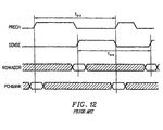
- Figure 12 shows an example of row access timing diagram for DRAMs with multiple banks.
- the period t SS specifies the minimum delay between sense operations to different banks.
- the period t PP specifies the minimum delay between precharge operations to different banks.
- Figure 13 is a more detailed diagram of a typical DRAM column datapath.
- the output of the column decoder which may be placed in a register for pipelined designs, drives a single column select line, which selects some fraction of outputs from the sense amplifiers.
- the selected sense amplifiers then drive the data on to the column I/O wires.
- the column I/O lines are typically differential and sensed using differential column amplifiers, which amplify small voltage differences on the column I/O wires and drive the data I/O bus to the interface.
- the width of the column I/O bus sets the data granularity of each column access, also known as CAS block granularity.
- the data I/O can either be bidirectional, in which write and read data are multiplexed on the same bus, or unidirectional, in which write and read data have separate buses.
- Figure 13 shows unidirectional data I/O.
- Column access power consists of the power to decode the column address, drive the column select line, turn on the column amplifiers, and drive the column I/O wires.
- Column power is roughly proportional to the column cycle frequency and the width of the column I/O datapath.
- Some DRAM cores also include the ability to mask write data, so that some bits or bytes of the datapath are not written depending on the mask pattern.
- the mask pattern is delivered to the column amplifier write circuit, which inhibits the write data appropriately.
- FIG. 14 A timing diagram for a column read operation is shown in Figure 14.
- the key timing parameters of the column read access are:
- a timing diagram for column write operation is shown in Figure 15. Many timing parameters, which include tPC, tCAS, tCP, tCLS, tCPS, tCLL, tCLH, tASC and tCAH, are the same as those for column read. Additional key timing parameters of the column write access are
- Typical column cycle times and access times greatly depend on the type of sense amplifier circuit, since the sense amplifier actually drives the data on to the column I/O wires. Increased speeds can be achieved by using more transistors in the sense amplifier circuit to improve drive capability, but this greatly increases the die area and cost since the sense amplifier circuit is heavily replicated. Thus, the desire to minimize die area for commodity DRAMs inhibits the further reduction of column access speeds.
- SRAM shares a similar core structure and functional blocks as DRAM. Like DRAM, access is performed in a similar two step process. First, in the sense operation, the information is transferred between the storage array and the sense amplifiers. Second, in the column access operation, the information is transferred between the sense amplifiers and the interface. Also, similar to DRAM, the bitlines must be precharged before sensing occurs, although a typical precharge value is Vdd, not Vdd/2.
- SRAM static random access memory
- data is stored statically, typically using a circuit of several transistors.
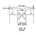
- a typical SRAM cell is shown in Figure 16.
- the SRAM of Figure 16 uses cross-coupled CMOS inverters to store a single data bit.
- a word line turns on access transistors, which connect the cell circuit to differential bit lines.
- the SRAM cell circuit actively drives the stored value on to the bit lines, thus resulting in faster access time.
- the static nature of the SRAM cell eliminates the need for cell refresh. However, the static cell also uses more transistors and takes up much more area than a DRAM cell.
- the four primitive operations of an SRAM are sense, precharge, read and write.
- Read-only memory cores store information according to an electrical connection at each cell site which joins rows to columns. Typically, a single transistor forms the electrical connection at each cell site.
- a simple ROM array is shown in Figure 17.
- ROM cell types including erasable programmable ROM (EPROM), electrically erasable programmable ROM (EEPROM), flash ROM, and mask programmable ROM. Their differences lie in the type of transistor used at the cell site. However, all ROM types share the common 2-D storage array organization, which requires a row and column decode of the address for each data access.
- EPROM erasable programmable ROM
- EEPROM electrically erasable programmable ROM
- flash ROM electrically erasable programmable ROM
- mask programmable ROM mask programmable ROM
- ROMs Unlike SRAMs or DRAMs, not all ROMs have sense amplifier circuits. Sense amplifiers are only used in some ROMs which require fast access times. For these ROMs, the primitive operations are sense, precharge and read.
- the data values are directly driven from the cell to output amps which drive the interface.
- the single primitive operation is read.
- Table 3 summarizes the primary operations for each memory type.
- this section describes the allowable sequences of operation for various memory types.
- composition of the operations cannot be arbitrary.
- memory cores that use sensing to speed row access such as conventional DRAMs and SRAMs
- a bank must be in a sensed state in order to do read or write operations.
- the bank must be precharged in order to perform a sense operation.
- these cores must follow the pattern shown in Figure 18 with respect to each bank's state, which can be either sensed ("open") or precharged ("closed”).
- an application will attempt to operate a sense amp memory core in a cached or uncached manner, depending upon the expected locality of reference from one application access to another. Combinations of these approaches are possible, but supporting arbitrary combinations can be an expensive proposition, resulting in either reduced performance or large resource usage both internally to the DRAM as well as externally in the interconnect.
- Operating the memory in an uncached manner means that the bank state is closed between application accesses. In other words, the last memory operation performed on that bank is a precharge. In such an operating manner, each application access typically consists of the sequence: sense, series of reads and/or writes, precharge. Uncached usage assumes low reference locality, i.e. subsequent memory access will likely not be located in the same row.
- Operating the memory in a cached manner means that the bank state is open between application accesses.
- the last memory operation performed on that bank is a sense, read, or write.
- Cached usage assumes high reference locality, i.e. subsequent memory access will likely be located in the same row.
- sense will not be the last memory operation performed since that implies that no useful work was done on behalf of the last application access.
- prefetching schemes which may have the last application access perform a sense with no corresponding read or write.
- the following operation can be read, write, or precharge. If it is a read or write, we call this a hit operation, since the row which was left cached in the bank must have been the proper row for the following operation. If it is a precharge, the correct row was not left cached in the bank, so the controller must apply a precharge and sense sequence in order to move the correct row into the bank. We call this type of access a miss operation.
- each application access typically consists of the sequence “series of reads and/or writes” (hit) or the sequence “precharge, sense, series of reads and/or writes” (miss).
- the optimal strategy for operating the DRAM depends upon the reference characteristics of the application. In the present invention either manner of operation, and mixed manners of operation, are supported.
- Figure 18 shows the operation sequencing for a generic memory core with sense amp caches. Variations of this diagram for different memory cores are also possible and are described in this section.
- Figure 19 shows operation sequencing for a DRAM, which is the same as that shown in Figure 18, except for the addition of the refresh sense and refresh precharge operations.
- Figure 20 shows an operation sequence for a common class of SRAMs whose sense amps only hold enough data for one read or write access. Note that transition 202, while possible, is not useful since it does not perform any useful work on behalf of the last application access. Also note that writes can occur after either precharge or sense, since the sense amplifiers in SRAMs are only used for read operations.
- Figure 21 shows an operation sequence for read-only memories with sense amps. Typically, sense amps only hold enough data for one read access. Note that transition 202, while possible, is not useful since it does not perform any useful work on behalf of the last application access.
- the interconnect also referred to as the channel.
- the signal propagation delay of the wire is greater than the bit time.
- the period of the bit rate is defined as the time it takes to transfer one bit; in the following examples, it is assumed that a bit is transferred on every clock edge, so the bit rate is 2x the clock frequency.
- the interconnect delay varies as a function of physical position on the channel, as Figure 22 illustrates. Note that the clock edges vary in time depending on the observation position.
- the interconnect has both 15 transmit and receive clocks going in opposite directions, and Figure 23 illustrates that the difference between transmit and receive clocks at a given position and time varies more than one clock cycle. It is also important to note that the interconnect delay for a given component doesn't change once its position is fixed.
- FIG. 3 shows a representation of a memory device with an interface and memory core. Internal delays in the core can vary from device to device due to process variations, circuit design differences, as well as variations in operation conditions that affect voltage and temperature.
- a memory core has four primary operations: precharge, sense, read, and write. Variations can occur in all components of core timing, which include the timing of row operations (sense and precharge), column operations (read and write) and interactions between row and column operations.
- Row timing is characterized by the timing parameters in Table 1 and illustrated in the timing diagram in Figure 11 (row timing).
- the row precharge time, tRP is the time it takes to precharge the sense amplifiers and bitlines inside a memory bank in the core. A bank must be precharged before a sense operation can occur.
- the minimum time between the start of a sense operation and the start of a precharge operation is tRAS,min.
- the minimum time between sense operations to the same memory bank is the row cycle time, tRC.
- Table 2 shows the basic column timing parameters, which are illustrated in the read and write timing diagrams in Figure 14 and Figure 15.
- tCAC is the delay between the latching of the column address and the delivery of read data to the core output.
- tCAC has two components: tCLS and tDAC.
- tCLS is the time between the rising edge of COLLAT (when column address is latched) and the rising edge of COLCYC (when data access from the sense amplifiers starts).
- tDAC is the time between the rising edge of COLCYC and when read data is delivered to the core output.
- tPC is the column cycle time, i.e. the minimum time between column operations.
- tRCD is the row to column delay and represents the time between the start of a sense operation and column operation (rising edge of COLCYC).
- tCPS is the column precharge to row precharge time and represents the time between the start of the column precharge (falling edge of COLCYC) and the start of the row precharge operation.
- All these core timings can vary widely across manufacturing processes, process generations, circuit designs, supply voltage fluctuations, and operating temperature. Furthermore, these core timing variations combine with interconnect delay variations to form accumulative system timing variations from device to device.
- Another desire is to minimize latency. For instance, for a device with a given tRCD, it would be desirable to provide enough fine-grain timing control between the row and column commands so that the delivery of the sense and column core control signals has an offset that closely matches tRCD. Any additional delay between the two commands would result in greater access latency.
- Timing adjustments can be done at either the transmitter or receiver. Since it is very desirable to keep the cost low, all mechanisms that perform timing adjustments, particularly in the memory devices, should have minimum complexity to keep die area and cost as low as possible.
- the memory controller will always operate at the speed of the slowest possible part and interconnect rather than adjusting for the actual speed of the devices or interconnect in a given system.
- interconnect delay In many existing synchronous memory systems, the interconnect delay is limited to a single clock cycle, so no interconnect delay compensation is needed.
- variations in row timing specifically tRAS,min, tRP, and tRCD, are "internally timed", i.e. row timing delays are handled with internal counters and programmable registers, which store cycle counts to match core timing.
- a single delay value that is programmable by changing the value in a register.
- the delay and range of the register are only designed to handle variations in device timing and not interconnect timing.
- a single delay value is used to cover multiple column read latency components, such as tCLS and tDAC.
- a register specifies the number of clock cycles between the column control and the column read data, as shown in Figure 26.
- the all encompassing delay provides a simple control model to the application that does not vary with internal memory device implementation details. However, this requires the memory device to decode for itself how the programmed delay should be used. This can be a very difficult problem since the delay of any one device is not known at design time. A further complication is that the period of the clock during operation is not known, even at final test time when the device delays can be measured. Simple methods for solving this problem are not obvious. Methods involving division of an internal memory device delay by the clock period are not considered simple.
- FIG 27 shows the interconnect structure of one such device, in which all row and column commands are issued over the same command bus. Also, the single address bus is shared for row and column operations. The row timing (tRP and tRAS,min) and row-to-column timing (tRCD, tCPS) variations are handled by adjusting the placement of control information over a single control bus resource. Because of conflicts, the overloading of both row and column commands on a single resource often limits the ability to perform fine timing control that optimally places row and column control to match actual device timings, as illustrated in Figure 28.
- existing memory devices have several inadequacies that limit optimal timing compensation in a high-speed pipelined memory system.
- First, existing devices are not designed to compensate for multicycle interconnect delay variation.
- Second, existing devices have a single shared interconnect control and/or address resource, which can limit the ability to have control over row timing and row-to-column timing variation when control information is packetized (occupies multiple cycles) and these parameters are not "internally timed”.
- timing variation of column access latency is typically controlled by a single number and not partitioned into the fundamental delay components that make up the column access latency in the core.
- Fourth, the column access to row precharge delay (tCPS) is considered, a fixed constant in the device and must be compensated by adjusting the timing of external control information.
- variations in column cycle time must be compensated by adjusting the timing of external control information.
- WO-A-97/23042 discloses a memory device having multiple adjustable delays associated with the row operation.
- Figure 4 of this document shows a precision delay circuit in an integrated circuit chip.
- the chip includes a transistor switching circuit in combination with a control circuit and a compensation circuit.
- the transistor switching circuit receives an input signal; and in response, the transistors switch on and off at an unpredictable speed to generate an output signal with a delay that has a large tolerance.
- the control circuit estimates the unpredictable speed at which the transistors switch and it generates control signals (SL, MED, FA) that identify the estimated speed.
- the compensation circuit receives the control signals from the control circuit; and in response, it selectively couples compensation components to the transistor switching circuit such that the combination of the transistors and the selectively coupled components generates the output signal with a precise delay.
- a memory device contains a memory core, a plurality of connections coupled to an interconnect structure for carrying column commands and row commands, and interface circuitry, coupled to said plurality of connections to receive said column commands and said row commands and coupled to said memory core to perform row and column operations on said memory core in accordance with said row commands and columns commands, said interface circuitry including multiple programmable delay components that correspond to respective specific portions of internal delays of said interface circuitry, wherein when said row commands and column commands are received with predefined timing offsets, the predefined timing offsets combined with delays associated with the programmable delay components match the timing between said row and column operations at said memory core.
- the channel has a time of flight which is multiple cycles in duration when the channel is long enough to have sufficient capacity.
- delay elements could be added to the data paths inside the memory components to get the logical layer to deliver read data to the channel in a fashion that eliminates logical device to device conflicts, or to "levelize" the channel. Note that this differs from the case where delay elements have not been used to handle interconnect delay variation.
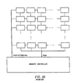
- Figure 29 shows devices with delay elements connected to a multicycle interconnect.
- the basic idea is to use these delay registers to add an appropriate amount of delay in each device, depending on position on the channel, so that the master sees a uniform minimum latency for all devices. Note that these delay registers are used to compensate interconnect delay, not device variation.
- the timing diagram of Figure 30 shows how the delay registers adjust for interconnect timing variation and allow the data interconnect to be fully packed.
- the figure shows four devices on the channel, each placed in a different clock domain, i.e. the signal propagation delay from the master equals 0, 1, 2, and 3 cycles for devices a, b, c, and d respectively.
- the delay registers in devices a, b, c, and d are programmed to be 3, 2, 1, and 0 cycles respectively.
- the timing diagrams in the figure show when the control packets are transmitted from the master and when the column operation begins (COLCYC pulse) for each device.
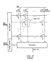
- a typical column read datapath is shown in Figure 31.
- the column logic After receiving a column control packet over the interconnect, the column logic initiates the column read operation in the core.
- the core control signals for column operations include bank and column addresses, a signal to latch the address (COLLAT), a signal to start the column operation (COLCYC, which stands for column cycle), and the signal to specify read or write (r/w).
- the column read operation is broken down into multiple steps. After some delay, the data appears at the ReadData output of the core. This data is then loaded into a storage element (e.g., latch) placed between the core and output datapath with a separate load control, LoadRd. The data is then separately loaded into the output datapath using a separate load signal (LoadPipe) and exits the interface.
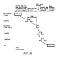
- a simplified timing diagram for the read operation is shown in Figure 32.
- Delaying the read data can be done by placing delay anywhere in the read datapath.
- One way to delay the read data is to delay the start of the column operation by delaying the column control signals to the core; this is called front-end leveling.
- the other approach is to delay the read data at the core output after the data exits the core; this is called back-end leveling.
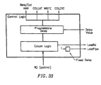
- Figure 33 shows the added delay block in the column logic block, which delays the issuance of the COLCYC command.
- the delay block can be programmable in order to allow variable delays.
- Figure 34 shows that by delaying COLCYC, the data is also delayed.
- Figure 35 shows the operation of two devices using front-end leveling. One device is shown with a leveling delay of 3 cycles and an interconnect delay of 0 cycles, the 'close' device. The lower device is shown with added delay of 0 cycles and an interconnect delay of 3 cycle, the 'far' device.
- the memory system It is desirable for the memory system to operate with the same control patterns and intervals for each device in the memory system. This reduces the complexity of the master, which would otherwise need to look up the specifics of each device as it performs memory operations. It also may increase bandwidth by maintaining a consistent repeating sequence for the different stages of the pipelined access to the memory devices.
- the controller can track the timing of each device, but this greatly increases controller complexity and the variable tRAS,min timing makes it hard to form an efficient pipeline.
- Figure 35 shows that the late read of the 'close' device defines the earliest time that a precharge may be performed to meet the constraint of t CPS,min .
- the read is positioned to show that for the 'far' device, the precharge could have been performed 3 cycles earlier and met both constraints, for t CPS,min and t RAS,min .
- the effective t RAS,min is 3 cycles longer than the actual t RAS,min of either device. This increases the occupancy time of a bank for any row, which can increase the latency to access a different row in the same bank and reduce performance.
- the delayed precharge may also prevent another bank from being precharged at the optimal time.
- the preferred method for delaying read data is to delay the data after it arrives from the core. This way, the timing of the core read operations stays fixed, and interactions with precharge are eliminated.
- Figure 36 shows that the problems shown in Figure 35 do not occur with back end leveling because the COLCYC positions are identical for the two devices.
- the column read datapath shown in Figure 31 shows separate load control points at both the latch and output datapath (LoadRd and LoadPipe).
- the interface provides two places to introduce read delay, and
- Figure 37 shows programmable delay elements used for both control signals. Both of these delay elements can be used to compensate for interconnect timing variation.
- Figure 38 illustrates the operation of delaying reads by delaying data to an output datapath.
- Figure 39 illustrates column read timing using the LoadRd and LoadPipe signals.
- the delay of LoadRd can also be used to allow for programmable variation in tDAC. In this case, any remaining delay not used for tDAC can be used to perform back-end leveling.
- Every memory device has delay variations due to process variation, circuit design, supply voltage, and operating temperature. These variations affect the row and column operation times, as well as the timing of interactions between row and column operations.
- the present invention include the following mechanisms to compensate for device-induced timing variations:
- the present invention includes the use of timing offsets between control commands sent over split control interconnect resources to provide finer control over internal device operations.
- the primary memory device operations are precharge, sense, column read, and column write.
- the device has an interconnect structure shown in Figure 41, where the control wires and internal control datapaths are split into separate precharge, sense, and column control buses.
- the timing diagram in Figure 42 shows how timing offsets can be used to control row timing and row to column timing for this embodiment.
- the controller can adjust the timing offsets between the sense, precharge, and column commands with clock cycle granularity to match the device timing for sense to column delay, tRCD, sense to precharge delay, tRAS,min, and precharge to sense delay, tRP.
- the figure shows the timing offsets for tRCD of 30 ns and 20 ns, tRAS,min of 50 ns and 42.5 ns, and tRP of 20 ns and 25 ns. Since the interconnect resources for sense and column are split and independent, fine timing control of these internal device operations is achieved.
- Another embodiment may combine interconnect resources to lower device and system cost. These compromises generally reduce the ability to finely control timing using offsets in favor of lower cost or higher latency (due to packetization of information).
- One example of this is to combine precharge and sense into a single interconnect resource, so that there are only sense/precharge and column control buses as shown in Figure 43. In this case the timing offsets technique cannot be used to control sense to precharge timing interactions, but can still be used to control sense to column (tRCD) and column to precharge (tCPS) timings.
- tRCD sense to column
- tCPS column to precharge
- Another example of this is to combine precharge and sense into a single interconnect resource and also combine column and precharge into another interconnect resource, such that precharge can be controlled from either resource.
- the present invention also uses multiple programmable delay mechanisms inside the device that match with internal device delay components to allow fine grain timing control.
- An example of this is the control of column read latency.
- the column read latency in the memory core, tCAC comprises two components originating from different parts of the column datapath: tCLS and tDAC, as Figure 14 shows.
- tCLS is the delay between the rising edge of COLLAT, when the column address is latched into the core, and the rising edge of COLCYC, when the column access begins and data is accessed from the sense amps in the core.
- Prior art devices have used delay elements to compensate for delay variation in column read latency, but have only used a single delay value to cover multiple column read latency components.
- the present invention differs from the prior art in that individual delay components are used that correspond to specific portions of the internal delays of the device.
- Dividing the coded delays into portions which correspond to internal memory device delays and making these available to the controller makes the division problem easy for the memory device since all decisions have been pushed back to the application layer. Now the burden is on the application to have enough intelligence to know the frequency of operation, read the device delay requirements, and use a method to program each one of them.
- the division problem can easily be performed in software and is eliminated from the memory device. The memory device only must present the proper control mechanisms so that the software can perform the task.
- Divided coded delays also provide finer grain timing control, which, for example, is useful in compensating for variations in processing, which may not affect each delay stage equally.
- Figure 31 shows the components of the column read path.
- the column read access latency, tCAC comprises two components: tCLS and tDAC.
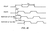
- Figure 44 shows one way to implement a programmable delay for tCLS, which delays the COLCYC control signal and effectively increases tCLS.
- the variation of tCLS is shown in Figure 45.
- Variable tDAC is achieved by delaying the LoadRd signal into the latch at the core output.
- the programmable delay of LoadRd can be used to compensate either variable tDAC or interconnect delay variation. Any remaining delay not used for tDAC can be used to perform back-end leveling to compensate for interconnect delay variation.
- timing parameters of column operations can also be programmable.
- the column to row precharge timing, tCPS as shown in the timing diagram in Figure 14, can be programmable by adding a programmable delay to the precharge signal that is triggered by the column logic and sent to the precharge state machine.
- tCAS the time between the rising and falling edges of COLCYC, can also be made programmable and can be useful depending on how the edges are used by the core. For instance, if a core design uses the rising edge to start the column access operation and falling edge to perform column precharge, the programmable tCAS would be very useful if there are timing variations in when the column precharge could begin after the column access starts. To implement this, a programmable delay element needs to be added to the COLCYC logic in order to allow variable timing of the falling edge.
- All of the device induced delay components can be statically compensated since, once compensated, they have no effect on channel bandwidth. They have only slight effect on average channel service time. Due to the relatively small effect on channel performance there is little to gain from dynamically coding the delays, especially since the critical path effects are significant.
- a receiver and transmitter can be combined in one device; a master and slave can be combined in one device; alternate embodiments may control different partitions of the column access path; alternate embodiments may use different mechanisms to control any controllable interval; methods can be used for any interconnect induced delay variations and any device which has an internal block which has various operations and delay constraints between those operations which vary; and the invention is not limited to devices with memory cores, but in general, any type of device.
Landscapes
- Dram (AREA)
- Information Transfer Systems (AREA)
- Memory System (AREA)
- Paper (AREA)
- Optical Communication System (AREA)
- Optical Recording Or Reproduction (AREA)
- Synchronisation In Digital Transmission Systems (AREA)
- Static Random-Access Memory (AREA)
Applications Claiming Priority (3)
| Application Number | Priority Date | Filing Date | Title |
|---|---|---|---|
| US6176997P | 1997-10-10 | 1997-10-10 | |
| US61769P | 1997-10-10 | ||
| PCT/US1998/021491 WO1999019876A1 (en) | 1997-10-10 | 1998-10-09 | Apparatus and method for device timing compensation |
Publications (2)
| Publication Number | Publication Date |
|---|---|
| EP1019911A1 EP1019911A1 (en) | 2000-07-19 |
| EP1019911B1 true EP1019911B1 (en) | 2003-07-16 |
Family
ID=22038016
Family Applications (1)
| Application Number | Title | Priority Date | Filing Date |
|---|---|---|---|
| EP98949806A Revoked EP1019911B1 (en) | 1997-10-10 | 1998-10-09 | Apparatus and method for device timing compensation |
Country Status (8)
| Country | Link |
|---|---|
| US (1) | US6226754B1 (enExample) |
| EP (1) | EP1019911B1 (enExample) |
| JP (3) | JP4578676B2 (enExample) |
| KR (1) | KR100618242B1 (enExample) |
| AT (1) | ATE245303T1 (enExample) |
| AU (1) | AU9604598A (enExample) |
| DE (1) | DE69816464T2 (enExample) |
| WO (1) | WO1999019876A1 (enExample) |
Families Citing this family (19)
| Publication number | Priority date | Publication date | Assignee | Title |
|---|---|---|---|---|
| US6154821A (en) * | 1998-03-10 | 2000-11-28 | Rambus Inc. | Method and apparatus for initializing dynamic random access memory (DRAM) devices by levelizing a read domain |
| US6643787B1 (en) | 1999-10-19 | 2003-11-04 | Rambus Inc. | Bus system optimization |
| US6646953B1 (en) | 2000-07-06 | 2003-11-11 | Rambus Inc. | Single-clock, strobeless signaling system |
| US6584576B1 (en) * | 1999-11-12 | 2003-06-24 | Kingston Technology Corporation | Memory system using complementary delay elements to reduce rambus module timing skew |
| US6516396B1 (en) * | 1999-12-22 | 2003-02-04 | Intel Corporation | Means to extend tTR range of RDRAMS via the RDRAM memory controller |
| US6658523B2 (en) * | 2001-03-13 | 2003-12-02 | Micron Technology, Inc. | System latency levelization for read data |
| US6675272B2 (en) * | 2001-04-24 | 2004-01-06 | Rambus Inc. | Method and apparatus for coordinating memory operations among diversely-located memory components |
| US7698441B2 (en) * | 2002-10-03 | 2010-04-13 | International Business Machines Corporation | Intelligent use of user data to pre-emptively prevent execution of a query violating access controls |
| DE10345550B3 (de) * | 2003-09-30 | 2005-02-10 | Infineon Technologies Ag | Speicheranordnung mit mehreren RAM-Bausteinen |
| DE102004016337A1 (de) * | 2004-04-02 | 2005-10-27 | Siemens Ag | Empfangsschaltung |
| US7669027B2 (en) * | 2004-08-19 | 2010-02-23 | Micron Technology, Inc. | Memory command delay balancing in a daisy-chained memory topology |
| US7248511B2 (en) * | 2005-02-24 | 2007-07-24 | Infineon Technologies Ag | Random access memory including selective activation of select line |
| US8327104B2 (en) * | 2006-07-31 | 2012-12-04 | Google Inc. | Adjusting the timing of signals associated with a memory system |
| US7940545B2 (en) * | 2008-06-24 | 2011-05-10 | Freescale Semiconductor, Inc. | Low power read scheme for read only memory (ROM) |
| US10566040B2 (en) | 2016-07-29 | 2020-02-18 | Micron Technology, Inc. | Variable page size architecture |
| US10892007B2 (en) | 2018-08-31 | 2021-01-12 | Taiwan Semiconductor Manufacturing Company, Ltd. | Variable delay word line enable |
| DE102018128927B4 (de) | 2018-08-31 | 2024-06-27 | Taiwan Semiconductor Manufacturing Co., Ltd. | Wortleitungsaktivierung für eine variable Verzögerung |
| JP6986127B1 (ja) * | 2020-10-21 | 2021-12-22 | 華邦電子股▲ふん▼有限公司Winbond Electronics Corp. | メモリシステムおよびその操作方法 |
| JP2025516288A (ja) * | 2022-05-04 | 2025-05-27 | アトメラ インコーポレイテッド | 消費電力を削減したdramセンスアンプアーキテクチャ及びそれに関する方法 |
Family Cites Families (23)
| Publication number | Priority date | Publication date | Assignee | Title |
|---|---|---|---|---|
| KR960003526B1 (ko) * | 1992-10-02 | 1996-03-14 | 삼성전자주식회사 | 반도체 메모리장치 |
| IL96808A (en) | 1990-04-18 | 1996-03-31 | Rambus Inc | Introductory / Origin Circuit Agreed Using High-Performance Brokerage |
| JPH04147492A (ja) * | 1990-10-11 | 1992-05-20 | Hitachi Ltd | 半導体メモリ |
| GB2250359A (en) | 1990-11-19 | 1992-06-03 | Anamartic Ltd | Addressing of chained circuit modules |
| JPH0567394A (ja) * | 1991-09-09 | 1993-03-19 | Seiko Epson Corp | 半導体記憶装置 |
| US5572722A (en) * | 1992-05-28 | 1996-11-05 | Texas Instruments Incorporated | Time skewing arrangement for operating random access memory in synchronism with a data processor |
| JPH0645892A (ja) * | 1992-08-24 | 1994-02-18 | Yamaha Corp | 信号遅延回路 |
| JPH06124230A (ja) * | 1992-10-09 | 1994-05-06 | Casio Electron Mfg Co Ltd | ダイナミックramアクセス制御装置 |
| JPH06273478A (ja) * | 1993-03-20 | 1994-09-30 | Hitachi Ltd | クロックスキュー補正回路、及び半導体集積回路 |
| JPH0745068A (ja) * | 1993-08-02 | 1995-02-14 | Mitsubishi Electric Corp | 同期型半導体記憶装置 |
| JPH0784863A (ja) * | 1993-09-20 | 1995-03-31 | Hitachi Ltd | 情報処理装置およびそれに適した半導体記憶装置 |
| EP0660329B1 (en) | 1993-12-16 | 2003-04-09 | Mosaid Technologies Incorporated | Variable latency, output buffer and synchronizer for synchronous memory |
| JP2991023B2 (ja) * | 1993-12-28 | 1999-12-20 | 株式会社日立製作所 | データ送信装置、データ送受信装置及びシステム |
| JPH08123717A (ja) * | 1994-10-25 | 1996-05-17 | Oki Electric Ind Co Ltd | 半導体記憶装置 |
| JPH08130448A (ja) * | 1994-10-31 | 1996-05-21 | Sanyo Electric Co Ltd | 可変遅延回路 |
| KR0146530B1 (ko) * | 1995-05-25 | 1998-09-15 | 김광호 | 단속제어회로를 구비한 반도체 메모리 장치와 제어방법 |
| US5600605A (en) | 1995-06-07 | 1997-02-04 | Micron Technology, Inc. | Auto-activate on synchronous dynamic random access memory |
| JPH09139074A (ja) * | 1995-11-10 | 1997-05-27 | Hitachi Ltd | ダイナミック型ram |
| EP0867068A1 (en) | 1995-12-15 | 1998-09-30 | Unisys Corporation | Delay circuit and memory using the same |
| US6043684A (en) * | 1995-12-20 | 2000-03-28 | Cypress Semiconductor Corp. | Method and apparatus for reducing skew between input signals and clock signals within an integrated circuit |
| JP3986578B2 (ja) * | 1996-01-17 | 2007-10-03 | 三菱電機株式会社 | 同期型半導体記憶装置 |
| JPH10340222A (ja) * | 1997-06-09 | 1998-12-22 | Nec Corp | メモリ装置の入力回路及び出力回路 |
| US5936977A (en) * | 1997-09-17 | 1999-08-10 | Cypress Semiconductor Corp. | Scan path circuitry including a programmable delay circuit |
-
1998
- 1998-10-09 WO PCT/US1998/021491 patent/WO1999019876A1/en not_active Ceased
- 1998-10-09 AT AT98949806T patent/ATE245303T1/de not_active IP Right Cessation
- 1998-10-09 US US09/169,687 patent/US6226754B1/en not_active Expired - Lifetime
- 1998-10-09 JP JP2000516350A patent/JP4578676B2/ja not_active Expired - Fee Related
- 1998-10-09 DE DE69816464T patent/DE69816464T2/de not_active Revoked
- 1998-10-09 AU AU96045/98A patent/AU9604598A/en not_active Abandoned
- 1998-10-09 KR KR1020007003857A patent/KR100618242B1/ko not_active Expired - Fee Related
- 1998-10-09 EP EP98949806A patent/EP1019911B1/en not_active Revoked
-
2008
- 2008-02-04 JP JP2008024238A patent/JP4579304B2/ja not_active Expired - Lifetime
- 2008-06-12 JP JP2008154645A patent/JP4870122B2/ja not_active Expired - Lifetime
Also Published As
| Publication number | Publication date |
|---|---|
| JP4870122B2 (ja) | 2012-02-08 |
| JP4578676B2 (ja) | 2010-11-10 |
| JP2008305537A (ja) | 2008-12-18 |
| KR20010031040A (ko) | 2001-04-16 |
| DE69816464T2 (de) | 2004-04-15 |
| AU9604598A (en) | 1999-05-03 |
| US6226754B1 (en) | 2001-05-01 |
| JP2001520431A (ja) | 2001-10-30 |
| ATE245303T1 (de) | 2003-08-15 |
| DE69816464D1 (de) | 2003-08-21 |
| WO1999019876A1 (en) | 1999-04-22 |
| JP2008210502A (ja) | 2008-09-11 |
| KR100618242B1 (ko) | 2006-09-04 |
| JP4579304B2 (ja) | 2010-11-10 |
| EP1019911A1 (en) | 2000-07-19 |
Similar Documents
| Publication | Publication Date | Title |
|---|---|---|
| US6226757B1 (en) | Apparatus and method for bus timing compensation | |
| JP4870122B2 (ja) | デバイスのタイミングを補償する装置及び方法 | |
| US7138823B2 (en) | Apparatus and method for independent control of on-die termination for output buffers of a memory device | |
| US10467158B2 (en) | Apparatuses and methods including memory commands for semiconductor memories | |
| US5844858A (en) | Semiconductor memory device and read and write methods thereof | |
| KR100326575B1 (ko) | 반도체 메모리 시스템 및 반도체 메모리의 액세스 제어 방법및 반도체 메모리 | |
| KR102722737B1 (ko) | 구성 가능한 메모리 어레이 뱅크 아키텍처를 위한 장치 및 방법 | |
| US6301183B1 (en) | Enhanced bus turnaround integrated circuit dynamic random access memory device | |
| US10872646B2 (en) | Apparatuses and methods for providing active and inactive clock signals | |
| EP1981033B1 (en) | Apparatus and method for pipelined memory operations with write mask | |
| CN101572118B (zh) | 半导体存储器装置及其存取方法 | |
| JP2004502267A (ja) | アクセス待ち時間が均一な高速dramアーキテクチャ | |
| JP2005222581A (ja) | 半導体記憶装置 | |
| US20070028027A1 (en) | Memory device and method having separate write data and read data buses | |
| US6463005B2 (en) | Semiconductor memory device | |
| US7830733B2 (en) | Devices, systems, and methods for independent output drive strengths | |
| JP4027709B2 (ja) | 半導体メモリ装置の入力回路 | |
| JP2002197864A (ja) | マルチポートメモリおよびその制御方法 | |
| USRE37753E1 (en) | Semiconductor memory device and read and write methods thereof | |
| JP5058295B2 (ja) | 半導体記憶装置 | |
| JP5048102B2 (ja) | 半導体記憶装置 | |
| EP1895538A1 (en) | Apparatus and method for pipelined memory operations |
Legal Events
| Date | Code | Title | Description |
|---|---|---|---|
| PUAI | Public reference made under article 153(3) epc to a published international application that has entered the european phase |
Free format text: ORIGINAL CODE: 0009012 |
|
| 17P | Request for examination filed |
Effective date: 20000510 |
|
| AK | Designated contracting states |
Kind code of ref document: A1 Designated state(s): AT BE CH DE FR GB IE IT LI LU NL |
|
| RIN1 | Information on inventor provided before grant (corrected) |
Inventor name: ABHYANKAR, ABHIJIT, M. Inventor name: TSERN, ELY, K. Inventor name: HAMPEL, CRAIG, E. Inventor name: STARK, DONALD, C. Inventor name: BARTH, RICHARD, M. Inventor name: WARE, FREDERICK, A. |
|
| 17Q | First examination report despatched |
Effective date: 20010509 |
|
| RAP1 | Party data changed (applicant data changed or rights of an application transferred) |
Owner name: RAMBUS INC. |
|
| GRAH | Despatch of communication of intention to grant a patent |
Free format text: ORIGINAL CODE: EPIDOS IGRA |
|
| GRAH | Despatch of communication of intention to grant a patent |
Free format text: ORIGINAL CODE: EPIDOS IGRA |
|
| GRAA | (expected) grant |
Free format text: ORIGINAL CODE: 0009210 |
|
| AK | Designated contracting states |
Designated state(s): AT BE CH DE FR GB IE IT LI LU NL |
|
| PG25 | Lapsed in a contracting state [announced via postgrant information from national office to epo] |
Ref country code: NL Free format text: LAPSE BECAUSE OF FAILURE TO SUBMIT A TRANSLATION OF THE DESCRIPTION OR TO PAY THE FEE WITHIN THE PRESCRIBED TIME-LIMIT Effective date: 20030716 Ref country code: LI Free format text: LAPSE BECAUSE OF FAILURE TO SUBMIT A TRANSLATION OF THE DESCRIPTION OR TO PAY THE FEE WITHIN THE PRESCRIBED TIME-LIMIT Effective date: 20030716 Ref country code: CH Free format text: LAPSE BECAUSE OF FAILURE TO SUBMIT A TRANSLATION OF THE DESCRIPTION OR TO PAY THE FEE WITHIN THE PRESCRIBED TIME-LIMIT Effective date: 20030716 Ref country code: BE Free format text: LAPSE BECAUSE OF FAILURE TO SUBMIT A TRANSLATION OF THE DESCRIPTION OR TO PAY THE FEE WITHIN THE PRESCRIBED TIME-LIMIT Effective date: 20030716 Ref country code: AT Free format text: LAPSE BECAUSE OF FAILURE TO SUBMIT A TRANSLATION OF THE DESCRIPTION OR TO PAY THE FEE WITHIN THE PRESCRIBED TIME-LIMIT Effective date: 20030716 |
|
| REG | Reference to a national code |
Ref country code: GB Ref legal event code: FG4D |
|
| REG | Reference to a national code |
Ref country code: CH Ref legal event code: EP |
|
| REG | Reference to a national code |
Ref country code: IE Ref legal event code: FG4D |
|
| REF | Corresponds to: |
Ref document number: 69816464 Country of ref document: DE Date of ref document: 20030821 Kind code of ref document: P |
|
| PGFP | Annual fee paid to national office [announced via postgrant information from national office to epo] |
Ref country code: NL Payment date: 20030919 Year of fee payment: 6 |
|
| PG25 | Lapsed in a contracting state [announced via postgrant information from national office to epo] |
Ref country code: LU Free format text: LAPSE BECAUSE OF NON-PAYMENT OF DUE FEES Effective date: 20031009 Ref country code: IE Free format text: LAPSE BECAUSE OF NON-PAYMENT OF DUE FEES Effective date: 20031009 |
|
| NLV1 | Nl: lapsed or annulled due to failure to fulfill the requirements of art. 29p and 29m of the patents act | ||
| REG | Reference to a national code |
Ref country code: CH Ref legal event code: PL |
|
| PLBI | Opposition filed |
Free format text: ORIGINAL CODE: 0009260 |
|
| PLBQ | Unpublished change to opponent data |
Free format text: ORIGINAL CODE: EPIDOS OPPO |
|
| ET | Fr: translation filed | ||
| PLAX | Notice of opposition and request to file observation + time limit sent |
Free format text: ORIGINAL CODE: EPIDOSNOBS2 |
|
| 26 | Opposition filed |
Opponent name: MICRON SEMICONDUCTORDEUTSCHLAND GMBH Effective date: 20040416 Opponent name: INFINEON TECHNOLOGIES AG Effective date: 20040416 Opponent name: MICRON EUROPE LTD Effective date: 20040408 |
|
| REG | Reference to a national code |
Ref country code: IE Ref legal event code: MM4A |
|
| PLAX | Notice of opposition and request to file observation + time limit sent |
Free format text: ORIGINAL CODE: EPIDOSNOBS2 |
|
| PLAX | Notice of opposition and request to file observation + time limit sent |
Free format text: ORIGINAL CODE: EPIDOSNOBS2 |
|
| PLBB | Reply of patent proprietor to notice(s) of opposition received |
Free format text: ORIGINAL CODE: EPIDOSNOBS3 |
|
| PLAQ | Examination of admissibility of opposition: information related to despatch of communication + time limit deleted |
Free format text: ORIGINAL CODE: EPIDOSDOPE2 |
|
| PLAR | Examination of admissibility of opposition: information related to receipt of reply deleted |
Free format text: ORIGINAL CODE: EPIDOSDOPE4 |
|
| PLBQ | Unpublished change to opponent data |
Free format text: ORIGINAL CODE: EPIDOS OPPO |
|
| PLAB | Opposition data, opponent's data or that of the opponent's representative modified |
Free format text: ORIGINAL CODE: 0009299OPPO |
|
| PLBP | Opposition withdrawn |
Free format text: ORIGINAL CODE: 0009264 |
|
| R26 | Opposition filed (corrected) |
Opponent name: MICRON SEMICONDUCTORDEUTSCHLAND GMBH Effective date: 20040416 Opponent name: MICRON EUROPE LTD Effective date: 20040408 |
|
| PLAY | Examination report in opposition despatched + time limit |
Free format text: ORIGINAL CODE: EPIDOSNORE2 |
|
| PLBC | Reply to examination report in opposition received |
Free format text: ORIGINAL CODE: EPIDOSNORE3 |
|
| PGFP | Annual fee paid to national office [announced via postgrant information from national office to epo] |
Ref country code: DE Payment date: 20071130 Year of fee payment: 10 |
|
| RDAF | Communication despatched that patent is revoked |
Free format text: ORIGINAL CODE: EPIDOSNREV1 |
|
| PGFP | Annual fee paid to national office [announced via postgrant information from national office to epo] |
Ref country code: IT Payment date: 20071029 Year of fee payment: 10 |
|
| PGFP | Annual fee paid to national office [announced via postgrant information from national office to epo] |
Ref country code: GB Payment date: 20071029 Year of fee payment: 10 Ref country code: FR Payment date: 20071017 Year of fee payment: 10 |
|
| RDAG | Patent revoked |
Free format text: ORIGINAL CODE: 0009271 |
|
| STAA | Information on the status of an ep patent application or granted ep patent |
Free format text: STATUS: PATENT REVOKED |
|
| 27W | Patent revoked |
Effective date: 20080222 |
|
| GBPR | Gb: patent revoked under art. 102 of the ep convention designating the uk as contracting state |
Effective date: 20080222 |
|
| PG25 | Lapsed in a contracting state [announced via postgrant information from national office to epo] |
Ref country code: FR Free format text: LAPSE BECAUSE OF NON-PAYMENT OF DUE FEES Effective date: 20061031 |
|
| PLAB | Opposition data, opponent's data or that of the opponent's representative modified |
Free format text: ORIGINAL CODE: 0009299OPPO |