EP1019911B1 - Appareil et procede de correction de la synchronisation de dispositifs - Google Patents
Appareil et procede de correction de la synchronisation de dispositifs Download PDFInfo
- Publication number
- EP1019911B1 EP1019911B1 EP98949806A EP98949806A EP1019911B1 EP 1019911 B1 EP1019911 B1 EP 1019911B1 EP 98949806 A EP98949806 A EP 98949806A EP 98949806 A EP98949806 A EP 98949806A EP 1019911 B1 EP1019911 B1 EP 1019911B1
- Authority
- EP
- European Patent Office
- Prior art keywords
- column
- timing
- memory
- delay
- row
- Prior art date
- Legal status (The legal status is an assumption and is not a legal conclusion. Google has not performed a legal analysis and makes no representation as to the accuracy of the status listed.)
- Revoked
Links
Images


Classifications
-
- G—PHYSICS
- G11—INFORMATION STORAGE
- G11C—STATIC STORES
- G11C7/00—Arrangements for writing information into, or reading information out from, a digital store
- G11C7/10—Input/output [I/O] data interface arrangements, e.g. I/O data control circuits, I/O data buffers
- G11C7/1072—Input/output [I/O] data interface arrangements, e.g. I/O data control circuits, I/O data buffers for memories with random access ports synchronised on clock signal pulse trains, e.g. synchronous memories, self timed memories
-
- G—PHYSICS
- G11—INFORMATION STORAGE
- G11C—STATIC STORES
- G11C7/00—Arrangements for writing information into, or reading information out from, a digital store
- G11C7/22—Read-write [R-W] timing or clocking circuits; Read-write [R-W] control signal generators or management
-
- G—PHYSICS
- G11—INFORMATION STORAGE
- G11C—STATIC STORES
- G11C7/00—Arrangements for writing information into, or reading information out from, a digital store
- G11C7/22—Read-write [R-W] timing or clocking circuits; Read-write [R-W] control signal generators or management
- G11C7/222—Clock generating, synchronizing or distributing circuits within memory device
Landscapes
- Dram (AREA)
- Information Transfer Systems (AREA)
- Memory System (AREA)
- Paper (AREA)
- Optical Communication System (AREA)
- Optical Recording Or Reproduction (AREA)
- Synchronisation In Digital Transmission Systems (AREA)
- Static Random-Access Memory (AREA)
Claims (9)
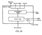
- Dispositif à mémoire comprenant :caractérisé en ce que :un noyau de mémoire ;une pluralité de connexions couplées à une structure d'interconnexion pour transporter des commandes de colonnes et des commandes de lignes ; etdes circuits d'interface couplés à ladite pluralité de connexions pour recevoir lesdites commandes de colonnes et lesdites commandes de lignes et couplés audit noyau de mémoire pour effectuer des opérations en lignes et en colonnes sur ledit noyau de mémoire en conformité avec lesdites commandes de lignes et lesdites commandes de colonnes ;lesdits circuits d'interface comportant de multiples composants de retard programmable qui correspondent à des parties spécifiques respectives de retards internes desdits circuits d'interface ;lorsque lesdites commandes de lignes et lesdites commandes de colonnes sont reçues avec des décalages temporels prédéterminés, les décalages temporels prédéterminés combinés à des retards. associés aux composants de retard programmable correspondent à la synchronisation entre lesdites opérations de lignes et de colonnes dans ledit noyau de mémoire.
- Dispositif à mémoire selon la revendication 1 dans lequel au moins deux desdits multiples composants de retard programmable sont positionnés en série dans un unique trajet de données des circuits d'interface de sorte que des retards associés aux au moins deux composants de retard programmable ont un effet cumulatif sur le fonctionnement du dispositif à mémoire.
- Dispositif à mémoire selon la revendication 1, dans lequel lesdits circuits d'interface comportent des circuits pour engendrer des signaux de synchronisation de noyau de mémoire correspondant auxdites commandes de lignes et auxdites commandes de colonnes, lesdits signaux de synchronisation de noyau de mémoire ayant des contraintes temporelles pour assurer un fonctionnement correct de noyau de mémoire, lesdits multiples composants de retard programmable comprenant une pluralité de composants de retard programmable individuels pour régler séparément la synchronisation des signaux sélectionnés de synchronisation de fonctionnement de lignes et des signaux de synchronisation de fonctionnement de colonnes desdits signaux de synchronisation de noyau de mémoire, de façon à satisfaire auxdites contraintes temporelles.
- Dispositif à mémoire selon la revendication 3, dans lequel lesdits circuits d'interface ajustent lesdits signaux de synchronisation de noyau de mémoire à la granularité du cycle d'horloge, par rapport à un signal d'horloge dont le cycle d'horloge est commandé de façon externe au dispositif à mémoire, afin d'adapter la synchronisation du dispositif au retard de la détection vers la colonne.
- Dispositif à mémoire selon la revendication 3, dans lequel lesdits circuits d'interface ajustent lesdits signaux de synchronisation de noyau de mémoire à la granularité de cycle d'horloge, par rapport à un signal d'horloge dont le cycle d'horloge est commandé à l'extérieur du dispositif à mémoire, afin d'adapter la synchronisation du dispositif au retard de la détection vers la précharge.
- Dispositif à mémoire selon la revendication 3 dans lequel lesdits circuits d'interface ajustent lesdits signaux de synchronisation de noyau de mémoire à la granularité du cycle d'horloge, par rapport à un signal d'horloge dont le cycle d'horloge est commandé à l'extérieur du dispositif à mémoire, afin d'adapter la synchronisation du dispositif au retard de la précharge vers la détection.
- Dispositif à mémoire selon la revendication 3 dans lequel lesdits circuits d'interface ajustent lesdits signaux de synchronisation de noyau de mémoire à la granularité du cycle d'horloge, par rapport à un signal d'horloge dont le cycle d'horloge est commandé à l'extérieur du dispositif à mémoire, afin d'adapter la synchronisation du dispositif au retard de la colonne vers la précharge.
- Dispositif à mémoire selon l'une quelconque des revendications précédentes 1 à 7, comportant au moins un composant de retard programmable qui est programmable de façon à compenser un retard latent de vol associé à une position du dispositif à mémoire sur un bus de communication.
- Dispositif à mémoire selon l'une quelconque des revendications précédentes 1 à 8, dans lequel les premier et second composants de retard programmable de ladite multiplicité de composants de retard programmable sont positionnés à l'intérieur de premier et second trajets de données distincts des circuits d'interface de sorte que des retards associés auxdits premier et second composants de retard affectent la synchronisation d'opérations différentes dans le dispositif à mémoire.
Applications Claiming Priority (3)
| Application Number | Priority Date | Filing Date | Title |
|---|---|---|---|
| US6176997P | 1997-10-10 | 1997-10-10 | |
| US61769P | 1997-10-10 | ||
| PCT/US1998/021491 WO1999019876A1 (fr) | 1997-10-10 | 1998-10-09 | Appareil et procede de correction de la synchronisation de dispositifs |
Publications (2)
| Publication Number | Publication Date |
|---|---|
| EP1019911A1 EP1019911A1 (fr) | 2000-07-19 |
| EP1019911B1 true EP1019911B1 (fr) | 2003-07-16 |
Family
ID=22038016
Family Applications (1)
| Application Number | Title | Priority Date | Filing Date |
|---|---|---|---|
| EP98949806A Revoked EP1019911B1 (fr) | 1997-10-10 | 1998-10-09 | Appareil et procede de correction de la synchronisation de dispositifs |
Country Status (8)
| Country | Link |
|---|---|
| US (1) | US6226754B1 (fr) |
| EP (1) | EP1019911B1 (fr) |
| JP (3) | JP4578676B2 (fr) |
| KR (1) | KR100618242B1 (fr) |
| AT (1) | ATE245303T1 (fr) |
| AU (1) | AU9604598A (fr) |
| DE (1) | DE69816464T2 (fr) |
| WO (1) | WO1999019876A1 (fr) |
Families Citing this family (17)
| Publication number | Priority date | Publication date | Assignee | Title |
|---|---|---|---|---|
| US6154821A (en) * | 1998-03-10 | 2000-11-28 | Rambus Inc. | Method and apparatus for initializing dynamic random access memory (DRAM) devices by levelizing a read domain |
| US6643787B1 (en) | 1999-10-19 | 2003-11-04 | Rambus Inc. | Bus system optimization |
| US6584576B1 (en) * | 1999-11-12 | 2003-06-24 | Kingston Technology Corporation | Memory system using complementary delay elements to reduce rambus module timing skew |
| US6516396B1 (en) * | 1999-12-22 | 2003-02-04 | Intel Corporation | Means to extend tTR range of RDRAMS via the RDRAM memory controller |
| US6658523B2 (en) * | 2001-03-13 | 2003-12-02 | Micron Technology, Inc. | System latency levelization for read data |
| US6675272B2 (en) * | 2001-04-24 | 2004-01-06 | Rambus Inc. | Method and apparatus for coordinating memory operations among diversely-located memory components |
| US7698441B2 (en) * | 2002-10-03 | 2010-04-13 | International Business Machines Corporation | Intelligent use of user data to pre-emptively prevent execution of a query violating access controls |
| DE10345550B3 (de) * | 2003-09-30 | 2005-02-10 | Infineon Technologies Ag | Speicheranordnung mit mehreren RAM-Bausteinen |
| DE102004016337A1 (de) * | 2004-04-02 | 2005-10-27 | Siemens Ag | Empfangsschaltung |
| US7669027B2 (en) | 2004-08-19 | 2010-02-23 | Micron Technology, Inc. | Memory command delay balancing in a daisy-chained memory topology |
| US7248511B2 (en) * | 2005-02-24 | 2007-07-24 | Infineon Technologies Ag | Random access memory including selective activation of select line |
| US8327104B2 (en) * | 2006-07-31 | 2012-12-04 | Google Inc. | Adjusting the timing of signals associated with a memory system |
| US7940545B2 (en) * | 2008-06-24 | 2011-05-10 | Freescale Semiconductor, Inc. | Low power read scheme for read only memory (ROM) |
| US10566040B2 (en) | 2016-07-29 | 2020-02-18 | Micron Technology, Inc. | Variable page size architecture |
| DE102018128927A1 (de) | 2018-08-31 | 2020-03-05 | Taiwan Semiconductor Manufacturing Co., Ltd. | Wortleitungsaktivierung für eine variable Verzögerung |
| US10892007B2 (en) | 2018-08-31 | 2021-01-12 | Taiwan Semiconductor Manufacturing Company, Ltd. | Variable delay word line enable |
| JP6986127B1 (ja) * | 2020-10-21 | 2021-12-22 | 華邦電子股▲ふん▼有限公司Winbond Electronics Corp. | メモリシステムおよびその操作方法 |
Family Cites Families (23)
| Publication number | Priority date | Publication date | Assignee | Title |
|---|---|---|---|---|
| KR960003526B1 (ko) * | 1992-10-02 | 1996-03-14 | 삼성전자주식회사 | 반도체 메모리장치 |
| IL96808A (en) | 1990-04-18 | 1996-03-31 | Rambus Inc | Introductory / Origin Circuit Agreed Using High-Performance Brokerage |
| JPH04147492A (ja) * | 1990-10-11 | 1992-05-20 | Hitachi Ltd | 半導体メモリ |
| GB2250359A (en) * | 1990-11-19 | 1992-06-03 | Anamartic Ltd | Addressing of chained circuit modules |
| JPH0567394A (ja) * | 1991-09-09 | 1993-03-19 | Seiko Epson Corp | 半導体記憶装置 |
| US5608896A (en) * | 1992-05-28 | 1997-03-04 | Texas Instruments Incorporated | Time skewing arrangement for operating memory devices in synchronism with a data processor |
| JPH0645892A (ja) * | 1992-08-24 | 1994-02-18 | Yamaha Corp | 信号遅延回路 |
| JPH06124230A (ja) * | 1992-10-09 | 1994-05-06 | Casio Electron Mfg Co Ltd | ダイナミックramアクセス制御装置 |
| JPH06273478A (ja) * | 1993-03-20 | 1994-09-30 | Hitachi Ltd | クロックスキュー補正回路、及び半導体集積回路 |
| JPH0745068A (ja) * | 1993-08-02 | 1995-02-14 | Mitsubishi Electric Corp | 同期型半導体記憶装置 |
| JPH0784863A (ja) * | 1993-09-20 | 1995-03-31 | Hitachi Ltd | 情報処理装置およびそれに適した半導体記憶装置 |
| EP0660329B1 (fr) * | 1993-12-16 | 2003-04-09 | Mosaid Technologies Incorporated | Tampon de sortie à latence variable et synchroniseur pour mémoire synchrone |
| JP2991023B2 (ja) * | 1993-12-28 | 1999-12-20 | 株式会社日立製作所 | データ送信装置、データ送受信装置及びシステム |
| JPH08123717A (ja) * | 1994-10-25 | 1996-05-17 | Oki Electric Ind Co Ltd | 半導体記憶装置 |
| JPH08130448A (ja) * | 1994-10-31 | 1996-05-21 | Sanyo Electric Co Ltd | 可変遅延回路 |
| KR0146530B1 (ko) | 1995-05-25 | 1998-09-15 | 김광호 | 단속제어회로를 구비한 반도체 메모리 장치와 제어방법 |
| US5600605A (en) | 1995-06-07 | 1997-02-04 | Micron Technology, Inc. | Auto-activate on synchronous dynamic random access memory |
| JPH09139074A (ja) * | 1995-11-10 | 1997-05-27 | Hitachi Ltd | ダイナミック型ram |
| WO1997023042A1 (fr) * | 1995-12-15 | 1997-06-26 | Unisys Corporation | Circuit de retard et memoire l'utilisant |
| US6043684A (en) * | 1995-12-20 | 2000-03-28 | Cypress Semiconductor Corp. | Method and apparatus for reducing skew between input signals and clock signals within an integrated circuit |
| JP3986578B2 (ja) * | 1996-01-17 | 2007-10-03 | 三菱電機株式会社 | 同期型半導体記憶装置 |
| JPH10340222A (ja) * | 1997-06-09 | 1998-12-22 | Nec Corp | メモリ装置の入力回路及び出力回路 |
| US5936977A (en) * | 1997-09-17 | 1999-08-10 | Cypress Semiconductor Corp. | Scan path circuitry including a programmable delay circuit |
-
1998
- 1998-10-09 US US09/169,687 patent/US6226754B1/en not_active Expired - Lifetime
- 1998-10-09 JP JP2000516350A patent/JP4578676B2/ja not_active Expired - Fee Related
- 1998-10-09 EP EP98949806A patent/EP1019911B1/fr not_active Revoked
- 1998-10-09 AU AU96045/98A patent/AU9604598A/en not_active Abandoned
- 1998-10-09 AT AT98949806T patent/ATE245303T1/de not_active IP Right Cessation
- 1998-10-09 DE DE69816464T patent/DE69816464T2/de not_active Revoked
- 1998-10-09 KR KR1020007003857A patent/KR100618242B1/ko not_active IP Right Cessation
- 1998-10-09 WO PCT/US1998/021491 patent/WO1999019876A1/fr active IP Right Grant
-
2008
- 2008-02-04 JP JP2008024238A patent/JP4579304B2/ja not_active Expired - Lifetime
- 2008-06-12 JP JP2008154645A patent/JP4870122B2/ja not_active Expired - Lifetime
Also Published As
| Publication number | Publication date |
|---|---|
| JP2008305537A (ja) | 2008-12-18 |
| JP2008210502A (ja) | 2008-09-11 |
| DE69816464D1 (de) | 2003-08-21 |
| JP4579304B2 (ja) | 2010-11-10 |
| KR20010031040A (ko) | 2001-04-16 |
| WO1999019876A1 (fr) | 1999-04-22 |
| JP4870122B2 (ja) | 2012-02-08 |
| JP4578676B2 (ja) | 2010-11-10 |
| AU9604598A (en) | 1999-05-03 |
| DE69816464T2 (de) | 2004-04-15 |
| ATE245303T1 (de) | 2003-08-15 |
| KR100618242B1 (ko) | 2006-09-04 |
| US6226754B1 (en) | 2001-05-01 |
| EP1019911A1 (fr) | 2000-07-19 |
| JP2001520431A (ja) | 2001-10-30 |
Similar Documents
| Publication | Publication Date | Title |
|---|---|---|
| US6226757B1 (en) | Apparatus and method for bus timing compensation | |
| JP4870122B2 (ja) | デバイスのタイミングを補償する装置及び方法 | |
| US7138823B2 (en) | Apparatus and method for independent control of on-die termination for output buffers of a memory device | |
| KR100326575B1 (ko) | 반도체 메모리 시스템 및 반도체 메모리의 액세스 제어 방법및 반도체 메모리 | |
| US10872646B2 (en) | Apparatuses and methods for providing active and inactive clock signals | |
| US6301183B1 (en) | Enhanced bus turnaround integrated circuit dynamic random access memory device | |
| US20070028027A1 (en) | Memory device and method having separate write data and read data buses | |
| US20190163652A1 (en) | Apparatuses and methods including memory commands for semiconductor memories | |
| EP1981033B1 (fr) | Appareil et procédé d'opérations de mémoire de pipeline avec masquage d'écriture | |
| US8422333B2 (en) | Semiconductor memory device and access method thereof | |
| JP2004502267A (ja) | アクセス待ち時間が均一な高速dramアーキテクチャ | |
| JP2005222581A (ja) | 半導体記憶装置 | |
| US6463005B2 (en) | Semiconductor memory device | |
| US7830733B2 (en) | Devices, systems, and methods for independent output drive strengths | |
| JP4027709B2 (ja) | 半導体メモリ装置の入力回路 | |
| JP2002197864A (ja) | マルチポートメモリおよびその制御方法 | |
| JP5048102B2 (ja) | 半導体記憶装置 | |
| JP5058295B2 (ja) | 半導体記憶装置 | |
| EP1895538A1 (fr) | Appareil et procédé d'opérations de mémoire de pipeline |
Legal Events
| Date | Code | Title | Description |
|---|---|---|---|
| PUAI | Public reference made under article 153(3) epc to a published international application that has entered the european phase |
Free format text: ORIGINAL CODE: 0009012 |
|
| 17P | Request for examination filed |
Effective date: 20000510 |
|
| AK | Designated contracting states |
Kind code of ref document: A1 Designated state(s): AT BE CH DE FR GB IE IT LI LU NL |
|
| RIN1 | Information on inventor provided before grant (corrected) |
Inventor name: ABHYANKAR, ABHIJIT, M. Inventor name: TSERN, ELY, K. Inventor name: HAMPEL, CRAIG, E. Inventor name: STARK, DONALD, C. Inventor name: BARTH, RICHARD, M. Inventor name: WARE, FREDERICK, A. |
|
| 17Q | First examination report despatched |
Effective date: 20010509 |
|
| RAP1 | Party data changed (applicant data changed or rights of an application transferred) |
Owner name: RAMBUS INC. |
|
| GRAH | Despatch of communication of intention to grant a patent |
Free format text: ORIGINAL CODE: EPIDOS IGRA |
|
| GRAH | Despatch of communication of intention to grant a patent |
Free format text: ORIGINAL CODE: EPIDOS IGRA |
|
| GRAA | (expected) grant |
Free format text: ORIGINAL CODE: 0009210 |
|
| AK | Designated contracting states |
Designated state(s): AT BE CH DE FR GB IE IT LI LU NL |
|
| PG25 | Lapsed in a contracting state [announced via postgrant information from national office to epo] |
Ref country code: NL Free format text: LAPSE BECAUSE OF FAILURE TO SUBMIT A TRANSLATION OF THE DESCRIPTION OR TO PAY THE FEE WITHIN THE PRESCRIBED TIME-LIMIT Effective date: 20030716 Ref country code: LI Free format text: LAPSE BECAUSE OF FAILURE TO SUBMIT A TRANSLATION OF THE DESCRIPTION OR TO PAY THE FEE WITHIN THE PRESCRIBED TIME-LIMIT Effective date: 20030716 Ref country code: CH Free format text: LAPSE BECAUSE OF FAILURE TO SUBMIT A TRANSLATION OF THE DESCRIPTION OR TO PAY THE FEE WITHIN THE PRESCRIBED TIME-LIMIT Effective date: 20030716 Ref country code: BE Free format text: LAPSE BECAUSE OF FAILURE TO SUBMIT A TRANSLATION OF THE DESCRIPTION OR TO PAY THE FEE WITHIN THE PRESCRIBED TIME-LIMIT Effective date: 20030716 Ref country code: AT Free format text: LAPSE BECAUSE OF FAILURE TO SUBMIT A TRANSLATION OF THE DESCRIPTION OR TO PAY THE FEE WITHIN THE PRESCRIBED TIME-LIMIT Effective date: 20030716 |
|
| REG | Reference to a national code |
Ref country code: GB Ref legal event code: FG4D |
|
| REG | Reference to a national code |
Ref country code: CH Ref legal event code: EP |
|
| REG | Reference to a national code |
Ref country code: IE Ref legal event code: FG4D |
|
| REF | Corresponds to: |
Ref document number: 69816464 Country of ref document: DE Date of ref document: 20030821 Kind code of ref document: P |
|
| PGFP | Annual fee paid to national office [announced via postgrant information from national office to epo] |
Ref country code: NL Payment date: 20030919 Year of fee payment: 6 |
|
| PG25 | Lapsed in a contracting state [announced via postgrant information from national office to epo] |
Ref country code: LU Free format text: LAPSE BECAUSE OF NON-PAYMENT OF DUE FEES Effective date: 20031009 Ref country code: IE Free format text: LAPSE BECAUSE OF NON-PAYMENT OF DUE FEES Effective date: 20031009 |
|
| NLV1 | Nl: lapsed or annulled due to failure to fulfill the requirements of art. 29p and 29m of the patents act | ||
| REG | Reference to a national code |
Ref country code: CH Ref legal event code: PL |
|
| PLBI | Opposition filed |
Free format text: ORIGINAL CODE: 0009260 |
|
| PLBQ | Unpublished change to opponent data |
Free format text: ORIGINAL CODE: EPIDOS OPPO |
|
| ET | Fr: translation filed | ||
| PLAX | Notice of opposition and request to file observation + time limit sent |
Free format text: ORIGINAL CODE: EPIDOSNOBS2 |
|
| 26 | Opposition filed |
Opponent name: MICRON SEMICONDUCTORDEUTSCHLAND GMBH Effective date: 20040416 Opponent name: INFINEON TECHNOLOGIES AG Effective date: 20040416 Opponent name: MICRON EUROPE LTD Effective date: 20040408 |
|
| REG | Reference to a national code |
Ref country code: IE Ref legal event code: MM4A |
|
| PLAX | Notice of opposition and request to file observation + time limit sent |
Free format text: ORIGINAL CODE: EPIDOSNOBS2 |
|
| PLAX | Notice of opposition and request to file observation + time limit sent |
Free format text: ORIGINAL CODE: EPIDOSNOBS2 |
|
| PLBB | Reply of patent proprietor to notice(s) of opposition received |
Free format text: ORIGINAL CODE: EPIDOSNOBS3 |
|
| PLAQ | Examination of admissibility of opposition: information related to despatch of communication + time limit deleted |
Free format text: ORIGINAL CODE: EPIDOSDOPE2 |
|
| PLAR | Examination of admissibility of opposition: information related to receipt of reply deleted |
Free format text: ORIGINAL CODE: EPIDOSDOPE4 |
|
| PLBQ | Unpublished change to opponent data |
Free format text: ORIGINAL CODE: EPIDOS OPPO |
|
| PLAB | Opposition data, opponent's data or that of the opponent's representative modified |
Free format text: ORIGINAL CODE: 0009299OPPO |
|
| PLBP | Opposition withdrawn |
Free format text: ORIGINAL CODE: 0009264 |
|
| R26 | Opposition filed (corrected) |
Opponent name: MICRON SEMICONDUCTORDEUTSCHLAND GMBH Effective date: 20040416 Opponent name: MICRON EUROPE LTD Effective date: 20040408 |
|
| PLAY | Examination report in opposition despatched + time limit |
Free format text: ORIGINAL CODE: EPIDOSNORE2 |
|
| PLBC | Reply to examination report in opposition received |
Free format text: ORIGINAL CODE: EPIDOSNORE3 |
|
| PGFP | Annual fee paid to national office [announced via postgrant information from national office to epo] |
Ref country code: DE Payment date: 20071130 Year of fee payment: 10 |
|
| RDAF | Communication despatched that patent is revoked |
Free format text: ORIGINAL CODE: EPIDOSNREV1 |
|
| PGFP | Annual fee paid to national office [announced via postgrant information from national office to epo] |
Ref country code: IT Payment date: 20071029 Year of fee payment: 10 |
|
| PGFP | Annual fee paid to national office [announced via postgrant information from national office to epo] |
Ref country code: GB Payment date: 20071029 Year of fee payment: 10 Ref country code: FR Payment date: 20071017 Year of fee payment: 10 |
|
| RDAG | Patent revoked |
Free format text: ORIGINAL CODE: 0009271 |
|
| STAA | Information on the status of an ep patent application or granted ep patent |
Free format text: STATUS: PATENT REVOKED |
|
| 27W | Patent revoked |
Effective date: 20080222 |
|
| GBPR | Gb: patent revoked under art. 102 of the ep convention designating the uk as contracting state |
Effective date: 20080222 |
|
| PG25 | Lapsed in a contracting state [announced via postgrant information from national office to epo] |
Ref country code: FR Free format text: LAPSE BECAUSE OF NON-PAYMENT OF DUE FEES Effective date: 20061031 |
|
| PLAB | Opposition data, opponent's data or that of the opponent's representative modified |
Free format text: ORIGINAL CODE: 0009299OPPO |