EP0940914B1 - Akustische oberflächenwellenanordnung und verfahren zur herstellung - Google Patents
Akustische oberflächenwellenanordnung und verfahren zur herstellung Download PDFInfo
- Publication number
- EP0940914B1 EP0940914B1 EP98929801A EP98929801A EP0940914B1 EP 0940914 B1 EP0940914 B1 EP 0940914B1 EP 98929801 A EP98929801 A EP 98929801A EP 98929801 A EP98929801 A EP 98929801A EP 0940914 B1 EP0940914 B1 EP 0940914B1
- Authority
- EP
- European Patent Office
- Prior art keywords
- film
- aluminum
- substrate
- crystal
- buffer metal
- Prior art date
- Legal status (The legal status is an assumption and is not a legal conclusion. Google has not performed a legal analysis and makes no representation as to the accuracy of the status listed.)
- Expired - Lifetime
Links
Images


Classifications
-
- H—ELECTRICITY
- H03—ELECTRONIC CIRCUITRY
- H03H—IMPEDANCE NETWORKS, e.g. RESONANT CIRCUITS; RESONATORS
- H03H9/00—Networks comprising electromechanical or electro-acoustic devices; Electromechanical resonators
- H03H9/02—Details
- H03H9/02535—Details of surface acoustic wave devices
- H03H9/02543—Characteristics of substrate, e.g. cutting angles
- H03H9/02559—Characteristics of substrate, e.g. cutting angles of lithium niobate or lithium-tantalate substrates
Definitions
- the present invention relates generally to a surface acoustic wave device, and its fabrication process, and more specifically to a surface acoustic wave device comprising a electrode film having improved power-durability, and its fabrication process.
- Surface acoustic wave devices i.e., surface acoustic wave filters or surface acoustic wave resonators are now increasingly used as an alternative to dielectric. filters for RF-band filters used with mobile communications equipment such as portable telephones and cordless telephones.
- a surface acoustic wave device especially a surface acoustic wave filter is smaller in size than a dielectric filter.
- the surface acoustic wave filter is superior in electrical performance to the dielectric filter, if they are of the same size.
- a surface acoustic wave device is made up of, at least, a piezoelectric substrate, a comb form of metal film electrode pattern formed on the surface of the piezoelectric substrate, and a package for housing both the piezoelectric substrate and the electrode pattern therein.
- Lithium niobate, lithium tantalate, quartz, etc. are used for the piezoelectric substrate.
- Lithium niobate, and lithium tantalate having a large electromechanical coupling coefficient are used especially for RF-band filters.
- Aluminum, etc. are used for the electrode pattern.
- Fig. 13 illustrates a general process sequence of steps of fabricating a prior art surface acoustic wave device.
- a metal film 51 for an electrode material is first formed as by vapor deposition or sputtering on a piezoelectric substrate 50 pre-washed at a step (a).
- a photoresist is coated on the metal film 51 as by spin coating.
- the photoresist is exposed to light according to a desired pattern using an exposure system, and developed to obtain a photoresist pattern 52, as depicted at a step (c).
- the metal film is etched, either wet or dry, at a step (c) into a desired electrode pattern 53.
- the photoresist used for pattern formation is removed at a step (e) using a stripping solution or by means of an ashing process.
- the pre-process called a photo-process finishes.
- the piezoelectric substrate with the electrode pattern formed thereon is diced at a step (f) into individual chips.
- each chip is fixed at a step (g) to a package using an bonding agent, after which bonding wires are interconnected at a step (h).
- a lid is welded at a step (i) to the package for ensuring airtightness, followed by performance inspection at a step (j).
- the so-called post-process comes to an end.
- a problem with the surface acoustic wave device when used at an RF-band of about 1 GHz is that the lifetime becomes short because the electrode finger width of the comb electrode and the space between electrode fingers become as fine as about 1 ⁇ m.
- a key determinant of the lifetime of the surface acoustic wave device is the power-durability of the electrode film.
- aluminum or Al was used for the reasons of its small specific gravity, and its low electric resistance.
- a problem with using aluminum for the electrode film is that the degradation of the electrode film becomes more pronounced as the applied frequency becomes higher.
- the repetitive stress applied on the electrode film gives rise to migration of aluminum atoms, which in turn causes electrode film defects such as hillocks, and voids, resulting in some considerable degradation of the performance of the surface acoustic wave device.
- the degradation of the electrode film becomes more pronounced as the applied frequency becomes higher and the applied power becomes larger.
- the higher the frequency the thinner the electrode film and the narrower the electrode width should be. Because of these and other factors, the electrode film is more likely to have defects as the applied frequency become higher. In other words, the power-durability of the surface acoustic wave device becomes low.
- J. I. Latham et al have disclosed the use of an aluminum-copper (Al-Cu) alloy obtained by adding to aluminum a trace amount of a different type metal such as copper (Cu) (Thin Solid Films, 64, pp. 9-15, 1979), and showed that by use of such an aluminum alloy it is possible to prevent occurrence of hillocks or voids on the electrode film and so improve the power-durability of a surface acoustic wave device.
- Al-Cu aluminum-copper
- Cu copper
- Fig. 10 is a scanning electron microscope photograph showing how an aluminum electrode film is degraded due to repetitive stress applied on a surface acoustic wave device. The fact that voids are found at grain boundaries of the aluminum electrode film supports that the migration of aluminum atoms occurs predominately at grain boundaries.
- JP-A 55-49014 Application of a substantial single-crystal form of material to an electrode film for a surface acoustic wave device has already been disclosed in JP-A 55-49014.
- the publication alleges that by use of an electrode material that is substantially a single crystal, it is possible to enhance the performance of a surface acoustic wave device, whatever material is used to make up the device.
- the publication shows that molecular beam epitaxy is preferred to obtain such an electrode film.
- the publication provides no disclosure of what is used for the substrate material, and how film-forming conditions are determined depending on the electrode material used. That is, what is disclosed therein is nothing else than general consideration to the effect that an improvement in the performance of a surface acoustic wave device is expectable by use of a single-crystal electrode film.
- the publication provides no illustrative disclosure of to what degree the Q value, and the aging properties are improved.
- Patent No. 2545983 One example of applying a single-crystal aluminum film or an aluminum film oriented in a certain crystal alignment direction to an electrode film for a surface acoustic wave device is disclosed in Patent No. 2545983.
- a rotated Y-cut quartz substrate in the 25° to 39° rotated Y-cut range is used as a piezoelectric substrate to obtain a (311) oriented film by vapor deposition at a high rate (a deposition rate of 40 ⁇ /sec.) and a low temperature (a substrate temperature of 80°C).
- the patent publication states that the film is an epitaxially grown film close to a single-crystal film.
- the patent publication suggests that an extremely thin Ti or Cr film is located at the interface between the quartz substrate and the aluminum film to such an extent that the orientation capability of the aluminum film is not inhibited.
- lithium niobate and lithium tantalate are often used as piezoelectric substrates, because of the magnitude of their electromechanical coupling coefficient.
- the patent publication discloses nothing about the use of lithium niobate and lithium tantalate; it refers merely to the (311) orientation of an aluminum film when quartz is used as a piezoelectric substrate.
- JP-A 5-90268 discloses a technique for providing a buffer metal layer on a piezoelectric substrate and forming a thin film form of aluminum or aluminum alloy thereon, and indicates that this structure allows the aluminum or aluminum alloy to show strong (111) orientation. So far, it has been known that the (111) oriented film of aluminum shows strong migration resistance. Consequently, the power-durability of a surface acoustic wave device should be improved by the (111) oriented electrode film.
- the example given therein teaches that the (111) oriented Al alloy film is obtained by using quartz as the piezoelectric substrate and forming a Ti buffer layer and an Al-0.5 wt% Cu alloy on the substrate in the described order, using a dual ion beam sputtering system.
- the publication teaches that the degree of the (111) orientation of the Al alloy was found from the strength of X-ray diffraction from the (111) plane, the full-width at half maximum of a rocking curve, etc. Insofar as the data about the widths of X-ray diffraction peaks and the full-widths at half maximum of rocking curves, given in the publication, are concerned, however, it appears that the obtained aluminum alloy is a polycrystalline film oriented strongly in the (111) direction.
- the above publication shows an example where lithium niobate useful for making up an RF-band filter is used as the piezoelectric substrate.
- vanadium (V), iron (Fe), cobalt (Co), nickel (Ni), copper (Cu), yttrium (Y), chromium (Cr), zinc (Zn), Fe 20 Ni 80 alloy, Ti 50 V 50 alloy, and Co 90 Ni 10 are used as a buffer metal, and 300 ⁇ aluminum is deposited on the buffer metal.
- the example teaches that the above metal and alloy species except zinc contribute to a decrease in specific resistance and an improvement in orientation capability.
- the obtained film is actually a polycrystalline film with the (111) plane oriented, because the full-widths at half maximum of rocking curves shown therein have a minimum value of 2.1 degrees.
- A. Kamijo and T. Mitsuzuka disclose similar results in an article, J. Appl. Phys. 77(8), pp. 3799-3804, 1995. From this article, it is found that when films are formed at an extremely low deposition rate by an ion beam sputtering process, for instance, an aluminum film is formed at 0.2 nm/sec. and a buffer metal film is formed at 0.04 to 0.2 nm/sec., an aluminum film strongly oriented in the (111) direction is obtained. However, this aluminum film is a polycrystalline film in the intra-planar direction thereof, and so the resulting electrode film is a polycrystalline film rather than a heteroepitaxial film.
- JP-A 5-199062 shows that an aluminum single-crystal film is used as a electrode film for a surface acoustic wave device, and discloses means for forming this aluminum single-crystal film.
- ST-or LST-cut quartz is used as a piezoelectric substrate.
- the publication alleges that by allowing the surface of this substrate to have an archipelagic structure wherein minute, hemispherical islands are almost uniformly present, it is possible to obtain an aluminum single-crystal film by a vapor deposition or sputtering process.
- the publication then teaches that a conventional etching process may be used as the technique for processing the surface of the substrate to impart the archipelagic structure thereto.
- the publication also teaches that a substrate material other than quartz, for instance, lithium niobate useful for making up an RF-band filter, too, is effective for use with this technique for obtaining a single-crystal aluminum film.
- a substrate material other than quartz for instance, lithium niobate useful for making up an RF-band filter, too, is effective for use with this technique for obtaining a single-crystal aluminum film.
- the publication discloses nothing about any illustrative example and data.
- JP-A 6-132777 discloses another prior art regarding an aluminum single-crystal film.
- the publication teaches that when a film is formed on an extremely thin and clean crystal plane at an extremely low deposition rate, an aluminum single-crystal film is obtained, and shows some examples wherein an aluminum single-crystal film may be formed on an LST-cut quartz substrate by a vacuum vapor deposition process, an aluminum single-crystal film may be formed on a 128° Y-cut lithium niobate substrate by a vacuum vapor deposition process, and an aluminum single-crystal film may be formed on a 112' X-cut lithium tantalate substrate by a vacuum vapor deposition process.
- the publication teaches that if the surface of the substrate is contaminated, no single-crystal film is then obtained.
- the deposition rate becomes slow, there is generally an increase in the probability of impurities, i.e., contaminant atoms arriving at, and being captured by, the surface of the substrate. It is thus expected that too slow a deposition rate makes it difficult to obtain a single-crystal film.
- the degree of vacuum of an atmosphere during deposition and the deposition rate are placed under precise control, it is then impossible to obtain a single-crystal film with high reproducibility. Thus, some problems arise in connection with mass production. To obtain a single-crystal film, it is important to reduce the kinetic energy of aluminum atoms arriving at the surface of the substrate.
- the power-durability of the aluminum electrode film used in the surface acoustic wave device becomes a matter of great concern.
- the following three methods have so far been proposed: one method where the electrode film is formed of an alloy, another method where the electrode film is formed of a film oriented in the (111) direction, and yet another method where the electrode film is formed of a single-crystal film.
- the alloy electrode film suffers from an increase in the loss in the surface acoustic wave device, which has an inevitable relation to an electric resistance increase.
- the electrode film formed of the film oriented in the (111) direction is improved in terms of power-durability due to the (111) orientation.
- the single-crystal electrode film is free from migration of aluminum atoms at grain boundaries because there are no grain boundaries, and can have decreased electric resistance.
- this single-crystal film may be best suited for use as a power-durable electrode material.
- the single-crystal film forming techniques disclosed in the above referred-to publications have several grave problems. For instance, the deposition system used costs much, the deposition rate is too slow for mass fabrication of surface acoustic wave devices, and the substrate used is limited to quartz.
- lithium niobate best suited for making up an RF-band filter where the power-durability of an electrode film is a matter of great concern, in particular a 64° rotated Y-cut lithium niobate piezoelectric substrate, how an aluminum electrode film is converted into a single-crystal film, and how a single-crystal aluminum electrode film is fabricated remains still unclarified.
- an aluminum, polycrystalline electrode film showing high (111) orientation is useful in view of power-durability.
- a (111) polycrystalline film showing high orientation is obtainable by forming a buffer metal on a piezoelectric substrate and forming an aluminum electrode film thereon.
- 36° rotated Y-cut lithium tantalate useful for making up an RF-band filter is used as the piezoelectric substrate to achieve high (111) orientation capability, what type of buffer film should be used, and at what thickness and under what conditions the buffer film should be formed remains still unclarified.
- the invention in its preferred embodiments advantageously provides at low cost a surface acoustic wave device comprising a 64° rotated Y-cut lithium niobate piezoelectric substrate and an electrode film formed thereon, which film comprises an aluminum single-crystal excellent in power-durability.
- the invention in its various aspects is defined below as (1) to (3).
- an aluminum (Al) film is formed on a lithium niobate piezoelectric substrate, especially a 64° rotated Y-cut substrate using titanium (Ti) as a buffer metal film, thereby obtaining a single-crystal film wherein the normal direction of the (001) crystal plane or c plane of the titanium buffer metal film is vertical to the substrate, and the normal direction of the (110) crystal plane of the aluminum film is vertical to the substrate.
- the power-durability of the electrode film can be much more increased than ever before.
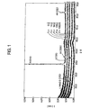
- Figure 1 is a chart showing changes in the X-ray diffraction pattern for an aluminum film with respect to changes in the thickness of a titanium buffer metal film when 64' rotated Y-cut lithium niobate is used as the substrate according to the invention.
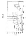
- Figure 2 is a chart showing changes in the X-ray diffraction pattern for an aluminum film with respect to changes in the thickness of a titanium buffer metal film when (100) Si is used as the substrate.
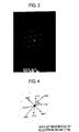
- Figure 3 is a drawing substitute photograph showing a selected-area electron diffraction pattern for a single-crystal aluminum film according to the invention.
- Figure 4 is a view showing the results of giving plane indices to the selected-area electron diffraction pattern shown in Fig. 3.
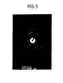
- Figure 5 is a drawing substitute photograph showing a selected-area electron diffraction pattern for a polycrystalline aluminum film.
- Figure 6 is a drawing substitute photograph showing a selected-area electron diffraction pattern for a single-crystal titanium buffer metal film according to the invention.
- Figure 7 is a view showing the results of giving plane indices to the selected-area electron diffraction pattern shown in Fig. 6.
- Figure 8 is a view of a measuring circuit for testing the power-durability of a surface acoustic wave device.
- Figure 9 is a drawing substitute photograph, i.e., a scanning electron microscope photograph showing the state of migration of aluminum atoms in a single-crystal aluminum film-containing electrode film.
- Figure 10 is a drawing substitute photograph showing a grain structure, i.e., a scanning electron microscope photograph showing the state of migration of aluminum atoms in an electrode film comprising polycrystalline aluminum.
- Figure 11 is a drawing substitute photograph showing a grain structure, i.e., a scanning electron microscope photograph of the surface of an aluminum film formed on a 64° rotated Y-cut lithium niobate substrate with a titanium buffer metal film interleaved between them.
- Figure 12 is a drawing substitute photograph showing a grain structure, i.e., a scanning electron microscope photograph of the surface of an aluminum film formed directly on a 64° rotated Y-cut lithium niobate substrate.
- Figure 13 illustrates a process sequence of steps of fabricating a surface acoustic wave device.
- the surface acoustic wave device comprises a 64° rotated Y-cut lithium niobate piezoelectric substrate and at least one pair of interdigital electrodes (comb electrode) formed on the surface of the substrate.
- the pair of interdigital electrodes comprise a titanium buffer metal film provided on the substrate and an aluminum film formed on the titanium buffer metal film.
- the above piezoelectric substrate is formed using a conventional 64° rotated Y-cut lithium niobate single crystal.
- the cut direction of the substrate may be confirmed by X-ray diffraction.
- the size of the substrate, when applied to a surface acoustic wave device is of the order of 2 to 10 mm in a surface acoustic wave propagation direction and of the order of 1 to 4 mm in a direction perpendicular thereto, and the thickness of the substrate is of the order of 0.2 to 0.4 mm.
- a round substrate of 2 inches or 3 inches in diameter is usually employed, and the above elements of the above sizes are formed together on the round substrate.
- the purity of titanium therein should preferably be as high as possible. However, it is acceptable to use a titanium buffer metal film having a titanium purity of at least 99.9%.
- the thickness of the titanium buffer metal film should preferably be at least 10 ⁇ .
- the upper limit to the thickness of the titanium buffer metal film is about 1 ⁇ m or lower, because as the titanium buffer metal film becomes thick, it is likely to crack or exfoliate due to increased internal stress.
- the titanium buffer metal film may be provided on the substrate by a vapor deposition process, a sputtering process or the like.
- the deposition rate for the titanium buffer metal film should preferably be of the order of 0.1 to 10 ⁇ /sec. in view of thickness control.
- the titanium buffer metal film according to the first aspect of the invention is a single-crystal film wherein the normal direction of the (001) plane is vertical to the substrate. This may be confirmed by relative position relationships among spots upon selected-area electron diffraction.
- the aluminum film may be formed on the titanium buffer metal film by a vapor deposition process, a sputtering process or the like.
- the deposition rate for the aluminum film should preferably be of the order of 10 to 50 ⁇ /sec.
- the thickness of the aluminum film may be determined depending on the frequency band applied, etc. However, it is generally preferable that the thickness of the aluminum film is determined in the range of 10 ⁇ to 3 ⁇ m inclusive, for the same reasons as explained in conjunction with the titanium buffer metal film.
- the aluminum film according to the first aspect of the invention is a single-crystal film wherein the normal direction of the (110) plane or a plane crystallographically equivalent thereto is vertical to the substrate. Whether or not the normal direction of the (110) plane of an aluminum crystal or a plane crystallographically equivalent thereto is vertical to the substrate may be confirmed from relative position relationships among spots on selected-area electron diffraction.
- the width of electrode fingers of the interdigital electrode made up of a multilayer film comprising the above titanium buffer metal film and aluminum film may be selected depending on the frequency used with a surface acoustic wave device. For instance, this width is generally of the order of 2 to 10 ⁇ m at a frequency band of 10 to 500 MHz.
- a sputtering system or the like may be used for an arrangement where a double-layer film can be obtained.
- Materials used for film deposition were aluminum with 99.999% purity, and titanium with 99.99% purity.
- the degree of vacuum reached during vapor deposition was 1.0 x 10 -4 Pa, and each substrate was heated at 100 to 150°C.
- the deposition rate was about 30 ⁇ /sec. for aluminum, and as low as about 1 ⁇ /sec. for titanium in view of ease of thickness control, because it was required to provide titanium in an extremely thin film form.
- each of the above three substrates was used to make a titanium buffer metal film-free sample (i.e., a sample consisting of an aluminum layer alone), and samples with titanium buffer metal films varying in thickness.
- the titanium buffer metal films were found to have a thickness of 16 ⁇ , 56 ⁇ , 138 ⁇ , and 1,065 ⁇ , respectively.
- an aluminum film was formed at a thickness of 1,800 ⁇ .
- the thicknesses of the titanium buffer metal films, and the aluminum film were measured by the fluorescent X-ray method.
- the thus prepared electrode films were inspected by X-ray diffraction. The results are shown in Fig. 1 and Fig. 2.
- Fig. 1 is a chart with X-ray diffraction patterns drawn in the same coordinate axes, said X-ray diffraction patterns found for an aluminum film formed on a 64LN substrate with no titanium buffer metal film formed thereon, and aluminum films formed on titanium buffer metal films with varying thicknesses, each provided on an 64LN substrate. It is found from Fig. 1 that, in the absence of the titanium buffer metal film, the aluminum film is strongly oriented in the (111) direction. In the presence of the titanium buffer metal films, however, the (111) orientation of aluminum vanishes. Irrespective of the thicknesses of the titanium buffer metal films in the thickness range under examination according to the invention, the peak for aluminum vanishes.
- Fig. 2 is a chart showing the results of similar X-ray diffraction in the case of Si substrates. In this case, too, the horizontal axes are shifted little by little to prevent peaks from overlapping each other. It was found that the substrate sample with no titanium buffer metal layer formed thereon produces a very strong (400) peak for Si. Thus, the remaining four samples were measured, skipping the angle out of which this Si (400) peak emerged. As can be seen from Fig. 2, the aluminum (111) orientation is more reinforced with an increasing thickness of the titanium buffer metal film, so that a polycrystalline aluminum film strongly oriented in the (111) direction can be obtained.
- the aluminum film of each sample was observed for its surface state under a scanning electron microscope (SEM). Consequently, when the substrates were made up of 36LT, and Si, the existence of crystal grains was confirmed regardless of the presence or absence of the titanium buffer metal films. When the substrates were made of 64LN, however, some noticeable changes were observed depending the presence or absence of the titanium buffer metal films. In other words, when the titanium buffer metal films were provided, it was found that within the thickness range under experimentation and investigation, all the aluminum films have a very smooth surface with no crystal grains at all. A scanning electron microscope photograph of a typical aluminum film with no crystal grains found thereon is attached hereto as Fig. 11. This aluminum film of 1,800 ⁇ in thickness was formed on the titanium buffer metal film of 56 ⁇ in thickness.
- Fig. 12 shows clearly grain boundaries whereas Fig. 11 shows no grain boundaries whatsoever.
- Fig. 3 shows a typical sample where spots manifest themselves upon selected-area electron diffraction.
- an aluminum film of 1,800 ⁇ in thickness was formed on a titanium buffer metal film of 56 ⁇ in thickness provided on a 64LN substrate.
- a sample having a titanium buffer metal film provided on a 64LN substrate it was confirmed that such spots as shown in Fig. 3 appear on a selected-area electron diffraction image of the aluminum film formed on the surface of the titanium buffer metal film, irrespective of the thickness of the latter.
- the criterion of judgment of whether or not a film is converted into a single-crystal film is generally whether or not streaks are found in addition to the emergence of spots.
- Fig. 5 shows a typical sample where a ring pattern manifests itself upon selected-area electron diffraction.
- aluminum was deposited on a 64LN substrate having no titanium buffer metal layer thereon.
- this sample showed a strong (111) orientation.
- the ring pattern was observed, indicating that the aluminum film is a polycrystalline film.
- Fig. 6 For the purpose of searching for why the aluminum film formed on the 64LN substrate with the titanium buffer metal film located between them is converted into a single crystal, selected-area electron diffraction was then performed for a sample having a titanium buffer metal film alone formed on a 64LN substrate.
- Fig. 7 shows plane indices given to the diffraction pattern.
- the direction of incidence of an electron beam aligns with the [001] axis direction.
- the titanium buffer metal film provided on the 64LN substrate is converted into a single-crystal film having the normal direction of its own (001) plane, i.e., the c plane vertical to the substrate.
- Fig. 6 shows the results of the sample having a titanium thickness of 1,065 ⁇ .
- the emergence of spots alone was observed, indicating that single-crystal films, each having the normal direction of the (001) plane vertical to the substrate, is obtained. From these, a possible mechanism, by which the aluminum single-crystal film can be formed, could be that the (001) plane of the titanium buffer metal film grows heteroepitaxially on the 64LN substrate, and the aluminum film formed on the (001) plane of titanium grows heteroepitaxially at its (110) plane.
- the surface acoustic wave device used for the estimation of power-durability was of the 3IDT longitudinal coupled double-mode type designed according to the receiving filter specification (center frequency: 947.5 MHz) for a GSM (European portable telephone) system.
- a 64° rotated Y-cut lithium niobate was used for the piezoelectric substrate, and an interdigital electrode made up of a single-crystal titanium buffer metal film and a single-crystal aluminum film was used for each IDT.
- Electrode finger width was about 1.2 ⁇ m
- electrode finger pitch or surface acoustic wave wavelength was 4.64 ⁇ m
- the number of pairs of electrode fingers were 17.5 pairs for the center IDT and 11 pairs for each outside IDT.
- a surface acoustic wave filter of the longitudinal coupled double-mode type was fabricated by providing a titanium buffer metal film of 350 ⁇ in thickness on a 36° rotated Y-cut lithium tantalate piezoelectric substrate, and forming an aluminum film thereon with a thickness of 0.35 ⁇ m, said aluminum film being a polycrystalline film which was oriented in the (111) direction and in which the rocking curve full-width at half maximum of its (111) peak was 2.0 degrees.
- the electrode pattern for this filter was the same as used in the filter for which the lithium niobate was used. Accordingly, the center frequency of the filter made up of the lithium tantalate substrate was shifted to a lower frequency side as compared with that of the GSM receiving side.
- a sample having an electrode made up of an aluminum polycrystalline film provided directly on the same 64° rotated Y-cut lithium niobate as mentioned above, and a sample using an Al-0.5 wt% Cu alloy, polycrystalline film as an electrode were also prepared. Electrode patterns for these samples, too, were the same as mentioned above. Used for the experimental frequency used for the estimation of power-durability, i.e., for lifetime testing was the frequency which is highest in the passband involved and at which power-durability becomes smallest. The acceleration conditions used were an ambient temperature of 80°C and an input power of 28 dBm. A measuring circuit used for power-durability experimentation is depicted in Fig. 8. Referring here to Fig.
- a high-frequency signal generated from an oscillator 61 is amplified by a high-frequency amplifier 62 to 28 dBm, and then applied via an isolator 68 on a surface acoustic wave filter 64 held in an 80'C thermostatic oven 63.
- This surface acoustic wave device i.e., surface acoustic wave filter 64 is connected to a high-frequency wattmeter 69.
- a network analyzer 65 is connected to both ends of the surface acoustic wave filter 64 via a directional coupler 70 and an attenuator 71.
- a controller 67 is connected to these units by way of a GP-IB cable 66.
- the lifetime of the device is here a period of time, TF (the time to failure), in which a 0.5 dB increase is found in the insertion loss of the filter.
- Power-durability testing was carried out using the aforesaid estimating system under the aforesaid acceleration conditions, and the results of testing were estimated on the aforesaid criterion of judgment.
- the TF upon power-durability testing of one comparative sample having the polycrystalline aluminum electrode film formed directly on the 64LN substrate was as short as 0.1 hour while the TF of another comparative sample with the electrode film made up of the Al-0.5 wt% Cu alloy, polycrystalline film was again as short as 2.8 hours.
- the power-durability of an electrode film having a single-crystal aluminum film formed according to the invention is about 19,000 times as long as that of an electrode film comprising a conventional aluminum polycrystalline film, and about 680 times as long as that of an electrode film comprising an Al-0.5 wt% Cu alloy, polycrystalline film proposed so far for power-durability improvements.
- Fig. 9 shows the results of an inventive sample in which a titanium buffer metal film was provided on a 64° rotated Y-cut lithium niobate substrate and an aluminum film was formed thereon, said titanium buffer metal film, and said aluminum film being a single-crystal film.
- Fig. 10 illustrates the state of the migration of aluminum atoms in a comparative polycrystalline aluminum electrode film after the power-durability acceleration testing. As can be seen from Fig. 10, voids are formed along grain boundaries. Thus, it appears that the migration of aluminum atoms occurs predominantly in the grain boundaries, as often pointed out in the prior art.
- the pure-aluminum film was formed on the titanium buffer metal film.
- impurity e.g., Cu
- Aluminum was deposited following the example with the exception that the deposition rate of aluminum was 10 ⁇ /sec. In this case, too, a single-crystal aluminum film was obtained as in the example.
- the vacuum vapor deposition process was used for film formation.
- the present invention may also be carried out with other film-formation processes, e.g., a sputtering process.
- the insertion loss was about 2.6 dB.
- a filter fabricated by forming a single-crystal aluminum film on a single-crystal titanium buffer metal film according to the invention was found to have an insertion loss of 2.4 dB. In terms of loss, too, a 0.2 dB improvement was achieved.
- the preferred surface acoustic wave device in accordance with the invention uses an electrode having satisfactory power-durability, and so is effective for increasing the lifetime of filters, for which fine comb electrodes must be used, e.g., RF-band filters used with mobile communications equipment.
Landscapes
- Physics & Mathematics (AREA)
- Acoustics & Sound (AREA)
- Chemical & Material Sciences (AREA)
- Engineering & Computer Science (AREA)
- Materials Engineering (AREA)
- Surface Acoustic Wave Elements And Circuit Networks Thereof (AREA)
Claims (3)
- Oberflächenakustikwellen-Vorrichtung, umfassend ein piezoelektrisches, um 64 ° gedrehtes Y-Schnitt-Lithiumniobat(V)-Substrat und eine darauf ausgebildete interdigitale Elektrode, dadurch gekennzeichnet, daß auf der interdigitalen Elektrode ein metallischer Titanpufferfilm und ein Aluminiumfilm ausgebildet sind, wobei sowohl der metallische Titanpufferfilm als auch der Aluminiumfilm Einkristallfilme sind, die sich bei der Feinbereichs-Elektronenbeugung lediglich in Form von Punkten manifestieren.
- Oberflächenakustikwellen-Vorrichtung nach Anspruch 1, wobei der metallische Titanpufferfilm eine Normale seiner (001)-Ebene senkrecht zum Substrat aufweist, und der Aluminiumfilm eine Normale seiner (110)-Ebene oder einer kristallographisch äquivalenten Ebene senkrecht zum Substrat aufweist.
- Verfahren zur Herstellung einer Oberflächenakustikwellen-Vorrichtung, die folgenden Schritte umfassend: Verwenden eines um 64 ° gedrehten Y-Schnitt-Lithiumniobat(V)-Substrats als piezoelektrisches Substrat und Bereitstellen eines metallischen Titanpufferfilms, bei dem es sich um einen Einkristallfilm handelt, der sich bei der Feinbereichs-Elektronenbeugung lediglich in Form von Punkten manifestiert; und Ausbilden eines Mehrschichtfilms, der den metallischen Titanpufferfilm und den Aluminiumfilm in einer interdigitalen Elektrodenkonfiguration umfaßt.
Applications Claiming Priority (5)
| Application Number | Priority Date | Filing Date | Title |
|---|---|---|---|
| JP27517397 | 1997-09-22 | ||
| JP27517397 | 1997-09-22 | ||
| JP28444397 | 1997-10-01 | ||
| JP28444397 | 1997-10-01 | ||
| PCT/JP1998/002981 WO1999016168A1 (fr) | 1997-09-22 | 1998-07-02 | Appareil a ondes acoustiques de surface et procede de fabrication de cet appareil |
Publications (3)
| Publication Number | Publication Date |
|---|---|
| EP0940914A1 EP0940914A1 (de) | 1999-09-08 |
| EP0940914A4 EP0940914A4 (de) | 2002-03-20 |
| EP0940914B1 true EP0940914B1 (de) | 2003-10-15 |
Family
ID=26551353
Family Applications (1)
| Application Number | Title | Priority Date | Filing Date |
|---|---|---|---|
| EP98929801A Expired - Lifetime EP0940914B1 (de) | 1997-09-22 | 1998-07-02 | Akustische oberflächenwellenanordnung und verfahren zur herstellung |
Country Status (5)
| Country | Link |
|---|---|
| US (1) | US6316860B1 (de) |
| EP (1) | EP0940914B1 (de) |
| CN (1) | CN1205744C (de) |
| DE (1) | DE69818972T2 (de) |
| WO (1) | WO1999016168A1 (de) |
Families Citing this family (26)
| Publication number | Priority date | Publication date | Assignee | Title |
|---|---|---|---|---|
| JP3266109B2 (ja) * | 1998-08-05 | 2002-03-18 | 株式会社村田製作所 | 電子デバイスの作製方法 |
| CN1109402C (zh) | 1999-05-31 | 2003-05-21 | Tdk株式会社 | 表面声波装置 |
| DE60035966T2 (de) | 1999-11-30 | 2008-03-20 | Tdk Corp. | Herstellungsverfahren für eine akustische oberflächenwellenvorrichtung |
| DE19960299A1 (de) * | 1999-12-14 | 2001-06-21 | Epcos Ag | Duplexer mit verbesserter Sende-/Empfangsbandtrennung |
| JP3846221B2 (ja) | 2000-07-14 | 2006-11-15 | 株式会社村田製作所 | 弾性表面波素子 |
| KR100791708B1 (ko) * | 2000-10-23 | 2008-01-03 | 마츠시타 덴끼 산교 가부시키가이샤 | 탄성 표면파 필터 및 그 제조 방법 |
| JP3521864B2 (ja) | 2000-10-26 | 2004-04-26 | 株式会社村田製作所 | 弾性表面波素子 |
| JP3445971B2 (ja) * | 2000-12-14 | 2003-09-16 | 富士通株式会社 | 弾性表面波素子 |
| JP3926633B2 (ja) * | 2001-06-22 | 2007-06-06 | 沖電気工業株式会社 | Sawデバイス及びその製造方法 |
| JP2003069357A (ja) * | 2001-08-28 | 2003-03-07 | Murata Mfg Co Ltd | 弾性表面波素子の製造方法および弾性表面波素子 |
| JP3735550B2 (ja) * | 2001-09-21 | 2006-01-18 | Tdk株式会社 | 弾性表面波装置およびその製造方法 |
| TWI282660B (en) | 2001-12-27 | 2007-06-11 | Murata Manufacturing Co | Surface acoustic wave device and manufacturing method therefor |
| JP3646116B2 (ja) * | 2003-07-17 | 2005-05-11 | Tdk株式会社 | 表面弾性波素子、表面弾性波装置、表面弾性波デュプレクサ、及び表面弾性波素子の製造方法 |
| JP2005347892A (ja) | 2004-05-31 | 2005-12-15 | Fujitsu Media Device Kk | 弾性表面波素子 |
| JP4809042B2 (ja) | 2005-11-10 | 2011-11-02 | 日本電波工業株式会社 | 弾性表面波素子及びその製造方法 |
| JP3961012B1 (ja) * | 2006-03-22 | 2007-08-15 | Tdk株式会社 | 弾性表面波装置 |
| US20090135541A1 (en) * | 2007-11-06 | 2009-05-28 | Kabushiki Kaisha Toshiba | Actuator and electronic circuit based thereon |
| US8664836B1 (en) * | 2009-09-18 | 2014-03-04 | Sand 9, Inc. | Passivated micromechanical resonators and related methods |
| DE102009056663B4 (de) | 2009-12-02 | 2022-08-11 | Tdk Electronics Ag | Metallisierung mit hoher Leistungsverträglichkeit und hoher elektrischer Leitfähigkeit und Verfahren zur Herstellung |
| JP5880520B2 (ja) * | 2013-10-30 | 2016-03-09 | 株式会社村田製作所 | 弾性波装置及びその製造方法 |
| EP3308178B1 (de) * | 2015-07-17 | 2019-11-06 | Hewlett-Packard Enterprise Development LP | Betriebsfrequenzbestimmung |
| CN106338347A (zh) * | 2016-11-02 | 2017-01-18 | 清华大学 | 一种高温声表面波传感器的叉指电极材料及其制备方法 |
| JP6986376B2 (ja) * | 2017-06-27 | 2021-12-22 | NDK SAW devices株式会社 | 弾性表面波素子およびその製造方法 |
| CN109297840B (zh) * | 2018-11-23 | 2021-09-17 | 辽宁工程技术大学 | 脉冲电压诱发薄膜材料机械疲劳测试方法及装置 |
| JP2020092321A (ja) | 2018-12-05 | 2020-06-11 | 太陽誘電株式会社 | 弾性波デバイスおよびその製造方法、フィルタ並びにマルチプレクサ |
| CN112737541B (zh) * | 2020-12-24 | 2023-09-29 | 北京航天微电科技有限公司 | 一种tc-saw谐振器、制作方法和滤波器 |
Family Cites Families (22)
| Publication number | Priority date | Publication date | Assignee | Title |
|---|---|---|---|---|
| JPS5549014A (en) | 1978-10-04 | 1980-04-08 | Seiko Instr & Electronics Ltd | Electrode for vibrating element |
| JPS5955615A (ja) * | 1982-09-24 | 1984-03-30 | Hitachi Ltd | 弾性表面波装置およびその製造方法 |
| JPS6480113A (en) | 1987-09-22 | 1989-03-27 | Hitachi Ltd | Surface acoustic wave device |
| JPH01128607A (ja) | 1987-11-13 | 1989-05-22 | Hitachi Ltd | 弾性表面波装置 |
| US5162690A (en) * | 1989-04-14 | 1992-11-10 | Murata Manufacturing Co., Ltd. | Surface acoustic wave device |
| JPH0314305A (ja) | 1989-06-13 | 1991-01-23 | Murata Mfg Co Ltd | 弾性表面波装置の製造方法 |
| JPH0410625A (ja) | 1990-04-27 | 1992-01-14 | Seiko Epson Corp | 電気配線の構造 |
| JP2937613B2 (ja) | 1991-07-16 | 1999-08-23 | 日本電気株式会社 | 薄膜配線およびその製造方法 |
| JPH05199062A (ja) | 1991-09-24 | 1993-08-06 | Seiko Epson Corp | 弾性表面波素子とその製造方法および弾性表面波素子用基板 |
| JPH05183373A (ja) * | 1991-12-30 | 1993-07-23 | Murata Mfg Co Ltd | 弾性表面波素子の電極材料 |
| JP3033331B2 (ja) | 1992-02-10 | 2000-04-17 | 日本電気株式会社 | 薄膜配線の製造方法 |
| JPH06132777A (ja) | 1992-10-20 | 1994-05-13 | Seiko Epson Corp | 弾性表面波素子とその製造方法 |
| JPH07107967A (ja) | 1993-10-15 | 1995-04-25 | Nippon Shokubai Co Ltd | 新規微生物 |
| JP2818535B2 (ja) * | 1993-11-11 | 1998-10-30 | 日本電気株式会社 | 弾性表面波装置 |
| JP3208977B2 (ja) | 1993-12-02 | 2001-09-17 | 株式会社村田製作所 | 弾性表面波素子の電極形成方法 |
| JPH07326943A (ja) * | 1994-06-02 | 1995-12-12 | Hitachi Ltd | 弾性表面波装置 |
| JPH08154030A (ja) * | 1994-11-25 | 1996-06-11 | Murata Mfg Co Ltd | 弾性表面波素子 |
| JP2888158B2 (ja) * | 1995-01-18 | 1999-05-10 | 日本電気株式会社 | 弾性表面波装置の製造方法 |
| JP3308749B2 (ja) * | 1995-01-27 | 2002-07-29 | 日本電気株式会社 | 弾性表面波装置の製造方法、および、これを用いて製造された弾性表面波装置 |
| JPH08288782A (ja) | 1995-02-15 | 1996-11-01 | Seiko Epson Corp | 弾性表面波素子、その製造方法及び電子機器 |
| EP0785299A1 (de) | 1996-01-19 | 1997-07-23 | Murata Manufacturing Co., Ltd. | Dünnmetallschicht und Verfahren zu ihrer Herstellung, akustische Oberflächenwellen anordnung enthaltend diese Schicht und Verfahren zu ihrer Herstellung |
| JPH09199969A (ja) * | 1996-01-19 | 1997-07-31 | Murata Mfg Co Ltd | 薄膜体 |
-
1998
- 1998-07-02 CN CNB988013851A patent/CN1205744C/zh not_active Expired - Lifetime
- 1998-07-02 WO PCT/JP1998/002981 patent/WO1999016168A1/ja active IP Right Grant
- 1998-07-02 DE DE69818972T patent/DE69818972T2/de not_active Expired - Fee Related
- 1998-07-02 EP EP98929801A patent/EP0940914B1/de not_active Expired - Lifetime
-
1999
- 1999-05-24 US US09/317,199 patent/US6316860B1/en not_active Expired - Lifetime
Also Published As
| Publication number | Publication date |
|---|---|
| EP0940914A4 (de) | 2002-03-20 |
| US6316860B1 (en) | 2001-11-13 |
| CN1205744C (zh) | 2005-06-08 |
| DE69818972D1 (de) | 2003-11-20 |
| EP0940914A1 (de) | 1999-09-08 |
| CN1239603A (zh) | 1999-12-22 |
| WO1999016168A1 (fr) | 1999-04-01 |
| DE69818972T2 (de) | 2004-07-22 |
Similar Documents
| Publication | Publication Date | Title |
|---|---|---|
| EP0940914B1 (de) | Akustische oberflächenwellenanordnung und verfahren zur herstellung | |
| EP1111779B1 (de) | Oberflächenwellenanordnung | |
| JP4809042B2 (ja) | 弾性表面波素子及びその製造方法 | |
| EP2288024B1 (de) | Oberflächenwellen-Bauelement und Verfahren zu seiner Herstellung | |
| CN100563100C (zh) | 表面声波装置 | |
| CA2020411C (en) | Surface acoustic wave device | |
| JP3609423B2 (ja) | 弾性表面波装置及びその製造方法 | |
| JP3735550B2 (ja) | 弾性表面波装置およびその製造方法 | |
| US5558711A (en) | Electrode forming method for surface acoustic wave device | |
| US7026743B2 (en) | Surface acoustic wave device having high dielectric strength and process for manufacturing the same | |
| TWI769270B (zh) | 聲表面波元件及其製造方法 | |
| US7146695B2 (en) | Method for manufacturing a surface acoustic wave device with a piezoelectric substrate | |
| Fujii et al. | Diamond wafer for SAW application | |
| Kimura et al. | High power-durable and low loss single-crystalline Al/Ti electrodes for RF SAW devices | |
| JP3317860B2 (ja) | 弾性表面波装置ならびにその製造方法 | |
| Dogheche et al. | Growth process and surface acoustic wave characteristics of LiNbO3/diamond/silicon multilayered structures | |
| JPH04365211A (ja) | 弾性表面波フィルタとその製造方法 | |
| JPH08139546A (ja) | 弾性表面波素子の電極形成方法 | |
| JPH07307634A (ja) | 弾性表面波素子電極の製造方法 | |
| KR19980083268A (ko) | 산화아연/질화알루미늄 2층박막을 이용한 탄성표면과 필터 제조방법 |
Legal Events
| Date | Code | Title | Description |
|---|---|---|---|
| PUAI | Public reference made under article 153(3) epc to a published international application that has entered the european phase |
Free format text: ORIGINAL CODE: 0009012 |
|
| 17P | Request for examination filed |
Effective date: 19990528 |
|
| AK | Designated contracting states |
Kind code of ref document: A1 Designated state(s): DE FR GB |
|
| A4 | Supplementary search report drawn up and despatched |
Effective date: 20020201 |
|
| AK | Designated contracting states |
Kind code of ref document: A4 Designated state(s): DE FR GB |
|
| RIC1 | Information provided on ipc code assigned before grant |
Free format text: 7H 03H 9/145 A, 7H 03H 9/25 B, 7H 03H 3/08 B, 7H 03H 9/02 B |
|
| 17Q | First examination report despatched |
Effective date: 20021105 |
|
| GRAH | Despatch of communication of intention to grant a patent |
Free format text: ORIGINAL CODE: EPIDOS IGRA |
|
| RBV | Designated contracting states (corrected) |
Designated state(s): DE FI GB |
|
| GRAS | Grant fee paid |
Free format text: ORIGINAL CODE: EPIDOSNIGR3 |
|
| GRAA | (expected) grant |
Free format text: ORIGINAL CODE: 0009210 |
|
| AK | Designated contracting states |
Kind code of ref document: B1 Designated state(s): DE FI GB |
|
| REG | Reference to a national code |
Ref country code: GB Ref legal event code: FG4D |
|
| REF | Corresponds to: |
Ref document number: 69818972 Country of ref document: DE Date of ref document: 20031120 Kind code of ref document: P |
|
| PLBE | No opposition filed within time limit |
Free format text: ORIGINAL CODE: 0009261 |
|
| STAA | Information on the status of an ep patent application or granted ep patent |
Free format text: STATUS: NO OPPOSITION FILED WITHIN TIME LIMIT |
|
| 26N | No opposition filed |
Effective date: 20040716 |
|
| PGFP | Annual fee paid to national office [announced via postgrant information from national office to epo] |
Ref country code: DE Payment date: 20080711 Year of fee payment: 11 |
|
| PGFP | Annual fee paid to national office [announced via postgrant information from national office to epo] |
Ref country code: FI Payment date: 20080714 Year of fee payment: 11 |
|
| PGFP | Annual fee paid to national office [announced via postgrant information from national office to epo] |
Ref country code: GB Payment date: 20080702 Year of fee payment: 11 |
|
| GBPC | Gb: european patent ceased through non-payment of renewal fee |
Effective date: 20090702 |
|
| PG25 | Lapsed in a contracting state [announced via postgrant information from national office to epo] |
Ref country code: FI Free format text: LAPSE BECAUSE OF NON-PAYMENT OF DUE FEES Effective date: 20090702 |
|
| PG25 | Lapsed in a contracting state [announced via postgrant information from national office to epo] |
Ref country code: GB Free format text: LAPSE BECAUSE OF NON-PAYMENT OF DUE FEES Effective date: 20090702 |
|
| PG25 | Lapsed in a contracting state [announced via postgrant information from national office to epo] |
Ref country code: DE Free format text: LAPSE BECAUSE OF NON-PAYMENT OF DUE FEES Effective date: 20100202 |