EP0928038B1 - Zweifrequenzschalter, anordnung mit gemeinsamer zweifrequenzantenne und mobile zweifrequenz-funkübertragungsausrüstung damit - Google Patents
Zweifrequenzschalter, anordnung mit gemeinsamer zweifrequenzantenne und mobile zweifrequenz-funkübertragungsausrüstung damit Download PDFInfo
- Publication number
- EP0928038B1 EP0928038B1 EP98923080A EP98923080A EP0928038B1 EP 0928038 B1 EP0928038 B1 EP 0928038B1 EP 98923080 A EP98923080 A EP 98923080A EP 98923080 A EP98923080 A EP 98923080A EP 0928038 B1 EP0928038 B1 EP 0928038B1
- Authority
- EP
- European Patent Office
- Prior art keywords
- terminal
- circuit
- switch
- dual band
- band
- Prior art date
- Legal status (The legal status is an assumption and is not a legal conclusion. Google has not performed a legal analysis and makes no representation as to the accuracy of the status listed.)
- Expired - Lifetime
Links
Images


Classifications
-
- H—ELECTRICITY
- H01—ELECTRIC ELEMENTS
- H01P—WAVEGUIDES; RESONATORS, LINES, OR OTHER DEVICES OF THE WAVEGUIDE TYPE
- H01P1/00—Auxiliary devices
- H01P1/10—Auxiliary devices for switching or interrupting
- H01P1/15—Auxiliary devices for switching or interrupting by semiconductor devices
Definitions
- the present invention relates to a dual band switch, a dual band antenna duplexer and a dual band mobile communication apparatus using the same, used mainly for a mobile communication device such as a portable telephone or the like.
- a popular conventional high frequency switch is disclosed in the non-examined Japanese Patent Application Publication No. H07-321692.
- a conventional switch is shown in Fig. 13.
- the switch of Fig. 13 comprises a circuit connecting in parallel PIN diode 1001 and compensation circuit 1002.
- Compensation circuit 1002 may be formed with a series connection of capacitor 1003 and inductor 1004.
- Compensation circuit 1002 may be used for turning off the switch circuit when PIN diode 1001 is in an inactive stateTherefore, compensation circuit 1002 may be set so that inductor 1004 cancels the parasitic capacitance of PIN diode 1001 in an inactive state, and may help create parallel resonance at a desired band.
- Capacitor 1003 may be referred to as a DC cut element for interrupting the direct current route of the compensation circuit when PIN diode 1001 becomes active and the switch circuit is turned on.
- compensation circuit 1002 may be adjusted to have an impedance which is capacitive in a frequency range close to a direct current and inductive in a desired band, as well as to have one series resonance point in-between.
- a diode high frequency SPDT switch which can be controlled by bias voltages, is described in JP-A-63 013 418.
- the switch comprises a parallel circuit of a diode and a serial resonance circuit composed of an inductance and a capacitor.
- the serial resonance circuit operates as a compensatory circuit for the diode by forming a parallel resonance circuit with the reverse capacitance of the diode in its OFF state. Hence, isolation of frequencies at the resonance frequency of the parallel resonance circuit is remarkable improved.
- the present invention addresses the aforementioned and other problems and aims to provide a dual band switch with which sufficient OFF states may be obtained in two different bands.
- a circuit in accordance with the present invention allows the impedance of the compensation circuit, which is capacitive in low frequency close to a direct current, to become inductive after the first series resonance point, whereby a parasitic capacitance of the diode is canceled in a first band. Further, the impedance of the compensation circuit becomes inductive again after the parallel resonance point and after the following series resonance point, whereby a parasitic capacitance of the diode is canceled in a second band.
- a dual band switch which assures sufficient OFF states in two different bands may thus be obtained with a relatively simple structure.
- Fig. 1 shows a dual band switch in a first exemplary embodiment of the present invention.
- the dual band switch comprises a circuit connecting in parallel PIN diode 101 and its compensation circuit 102.
- Compensation circuit 102 includes a circuit which serially connectsa serial resonance circuit, formed with first capacitor 103 and first inductor 104, with a parallel resonance circuit formed with second capacitor 105 and second inductor 106.
- the impedance of compensation circuit 102 is capacitive at low frequency (close to a direct current), at which the effect of capacitor 103 is dominant. Then, after a series resonance point, created by the combined impedance of first inductor 104, second capacitor 105 and second inductor 106, and first capacitor 103, the impedance of compensation circuit 102 becomes inductive. Hence, a parasitic capacitance of PIN diode 101 in an inactive state may be canceled in a first band, and accordingly the switch may attain a sufficient OFF state in the first band.
- the impedance of compensation circuit 102 may become capacitive again. Further, after the series resonance point created by the combined impedance of first capacitor 103 and first inductor 104, and the parallel resonance circuit, the impedance of compensation circuit 102 becomes inductive again. Hence, a parasitic capacity of PIN diode 101 in an inactive state may be canceled in a second band, and accordingly the switch may attain a sufficient OFF state in the second band.
- first capacitor 103 functions as a so called direct current cut element for interrupting the direct current route of compensation circuit 102.
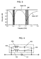
- Fig. 2 shows reactance characteristics at an OFF state of the dual band switch of this exemplary embodiment of the present invention.
- X1 represents reactance by parasitic capacitance of PIN diode 101 in an inactive state
- X2 represents reactance of compensation circuit 102.
- the parasitic capacitance may be substantially canceled in first band M1 and second band M2 by connecting in parallel compensation circuit 102, having two series resonance points r1, r2 and one parallel resonance point al, with diode 101.
- insertion loss at switch ON is less than 0.5dB in all bands, and, at switch OFF, an isolation of more than 25 dB is obtained in the first band M1 (890 - 960 MHz) and second band (1710 - 1880 MHz).
- Compensation circuit 102 of Fig. 1 is formed by a series circuit of a series resonance circuit and a parallel resonance circuit.
- a compensation circuit may also be formed by a circuit connecting in parallel two series resonance circuits as shown in Fig. 4. Namely, two series resonance circuits are respectively formed with first capacitor 403 and first inductor 404, and with second capacitor 405 and second inductor 406. These two series circuits may then be connected in parallel to form compensation circuit 102.
- This circuit arrangement has a characteristic which is capacitive at low frequency (close to direct current) having two series resonance points and one parallel resonance point.
- Both the compensation circuit 102 of Fig. 4 and the compensation circuit 102 of Fig. 1 have substantially the same impedance characteristics as shown in Fig. 2, and substantially the same transmission characteristics as shown in Fig. 3. Therefore, using the compensation circuit of Fig. 4, a dual band switch that attains a sufficient OFF state in two bands M1, M2 may be realized.
- a bias circuit comprising a resistor, an inductor and a bypass capacitor, may be needed for putting the PIN diode into an active state.
- a direct current cut capacitor may be used at each terminal for preventing a direct current.
- the structure of a high frequency switch circuit of the terminal may be simplified by using a dual band switch in accordance with an embodiment of the present invention.
- the terminal may thus be reduced both in size and weight.
- Fig. 5 shows a dual band switch in accordance with a second exemplary embodiment of the present invention.
- first PIN diode 701 may be connected, and between second terminal 709 and common terminal 708, second PIN diode 710 may be connected.
- the cathodes of PIN diodes 701 and 710 may be connected to common terminal 708.
- a series resonance circuit formed with first capacitor 703 and first inductor 704, and a parallel resonance circuit formed with second capacitor 705 and second inductor 706 may be connected in series forming first compensation circuit 702.
- First compensation circuit 702 may then be connected in parallel with first PIN diode 701 forming first switch 717.
- a series resonance circuit formed with third capacitor 712 and third inductor 713, and a parallel resonance circuit formed with fourth capacitor 714 and fourth inductor 715 may be connected in series forming second compensation circuit 711.
- Second compensation circuit 711 may then be connected in parallel with second PIN diode 710 forming second switch 718.
- Choke coil 716 may be connected between common terminal 708 and ground.
- first switch 717 and of second switch 718 are substantially the same.
- first switch 717 and second switch 718 independently operate as the dual band switch of Fig. 1.
- second switch 718 When first switch 717 is turned on by applying a direct current, as second PIN diode 710 substantially prevents the flow of current and as third capacitor 712 of second compensation circuit 711 cuts the direct current component substantially, all direct current flows into choke coil 716. Thus, second switch 718 is turned off. Also, second compensation circuit 711, as described in the first exemplary embodiment, acts to cancel a parasitic capacitance of second PIN diode 710 in two bands (M1 and M2), the impedance of second switch 718 from the side of common terminal 708 is relatively high in the two bands. Accordingly, in these two bands (M1 and M2), the input signal fed from first terminal 707 may be output to common terminal 708, and may not be output to second terminal 709.
- first diode 701 substantially prevents the flow of current and first capacitor 703 of first compensation circuit 702 cuts the direct current component, substantially all direct current flows into choke coil 716 Thus, first switch 717 is turned off.
- first compensation circuit 702 acts to substantially cancel a parasitic capacitance of first PIN diode 701 in two bands (M1 and M2), the impedance of first switch 717 from the side of common terminal 708 is relatively high in these two bands. Accordingly, in the two bands (M1 and M2), an input signal fed from common terminal 708 may be output to second terminal 709, and may not be output to first terminal 707.
- the circuit arrangement of Fig. 5 may enable the realization of a dual band SPDT switch which functions in two bands (Mland M2) to selectively and separately turn on first switch 717 and second switch 718.
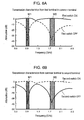
- Figs. 6Aand 6B show transmission characteristics of a dual band SPDT switch in accordance with the second exemplary embodiment of the present invention.
- the transmission characteristics from first terminal 707 to common terminal 708 show that, at an ON state of first switch 717, an insertion loss in first band M1 and second band M2 is less than 0.5dB, further, at an OFF state of first switch 717, an isolation of more than 25dB may be attained in both bands M1 and M2.
- the transmission characteristics from common terminal 708 to second terminal 709 show that, at an ON state of second switch 718, an insertion loss is less than 0.5dB in first band M1 and in second band M2. Further, at an OFF state of second switch 718, an isolation of more than 25dB may be attained in both bands M1 and M2.
- a relatively good characteristics for a dual band SPDT switch may be attained by making a circuit arranged as in this exemplary embodiment.
- each of first switch 717 and second switch 718 may be formed with the circuit shown in Fig. 1.
- these switches may also be formed with the circuit shown in Fig.4.
- a bias circuit comprising a resistor, an inductor and a bypass capacitor may be used for each switch for putting the PIN diode into an active state.
- a direct current cut capacitor may be used at each terminal for preventing a direct current.
- the structure of a high frequency switch circuit of the terminal may be simplified by using a dual band switch in accordance with an embodiment of the present invention.
- the terminal may thus be reduced both in size and weight.
- Fig. 7 shows a dual band switch in accordance with a third exemplary embodiment of the present invention.
- first switch 827 has the same structure as that of first switch 717 of the second exemplary embodiment. Therefore, the same reference numerals are used and a detailed explanation of the operation of first switch 827 is not repeated.
- first switch 827 to common terminal 708, one end of first switch 827, one end of third capacitor 817, and one end of a third inductor 818 may be connected to common terminal 708. Another end of the third capacitor 817 may be grounded. To another end of third inductor 818, one end of fourth capacitor 819, one end of fourth inductor 820, and an anode of second PIN diode 822 may be connected. Another end of fourth capacitor 819 may be grounded. Another end of fourth inductor 820 forms second terminal 709, to which one end of fifth capacitor 821 and an anode of third PIN diode 826 are connected. Another end of fifth capacitor 821 may be grounded.
- compensation circuit 823 which comprises a parallel resonance circuit formed with sixth capacitor 824 and fifth inductor 825, may be connected. Another end of second compensation circuit 823 may be grounded. A cathode of third PIN diode 826 may be grounded. Hence, second switch 828 may be formed between common terminal 708 and second terminal 709.
- phase of first phase shift circuit 829 may be set to be approximately 90° in a second band (e.g. M2 in the second exemplary embodiment), and a total phase of first phase shift circuit 829 and of second phase shift circuit 830 may be set to be approximately 90° in a first band (e.g. M1 in the second exemplary embodiment).
- Second compensation circuit 823 may be set to attain parallel resonance in a first band M1, and to attain series resonance with second PIN diode 822, in an active state, in a second band M2.
- first switch 827 When a direct current is applied by applying a bias to a forward direction of first PIN diode 701, first switch 827 may be turned on as described in the first exemplary embodiment of the present invention.
- the direct current flows into second PIN diode 822 and to third diode 826, and both diodes become active.
- second band M2 second PIN diode 822, in an active state, and second compensation circuit 823 attain a state of series resonance.
- the phase of first phase shift circuit 829 may change by approximately 90°.
- the impedance of second switch 828 becomes relatively high from the side of common terminal 708.
- first band M1 As second compensation circuit 823 attains a state of parallel resonance, the effect of second PIN diode 822 becomes negligible with regard to high frequency, and as since a total of the phase of first phase shift circuit 829 and the phase of second phase shift circuit 830 becomes approximately 90°, the impedance of the second switch 828 becomes relatively high from the side of the common terminal 708.
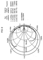
- Fig. 8 shows an impedance characteristics of switch 828 from the side of common terminal 708 in this situation.
- a region between markers 1 and 2 represents first band M1 (e.g. 890 - 960MHz)
- second band M2 e.g. 1710 - 1880MHz).
- first switch 827 when a bias is not applied to terminal 707, first switch 827 may be turned off in both first band M1 and second band M2 as described above in the first exemplary embodiment. In this case, the impedance of switch 827 from the side of common terminal 708 becomes high in both bands (M1 and M2). Further, both second PIN diode 822 and third PIN diode 826 may become inactive, and second switch 828 behaves substantially as first phase shift circuit 829 and second phase shift circuit 830. Hence, a signal fed from common terminal 708 is transmitted to second terminal 709 substantially unchanged. In other words, second switch 828 is turned on.
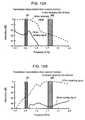
- Fig. 9A-9B shows transmission characteristics of the dual band SPDT switch of this exemplary embodiment.
- the transmission characteristics from first terminal 707 to common terminal 708 show that when the bias is ON, an insertion loss is less than 0.5dB in both first band M1 and second band M2, while when the bias is OFF, an isolation of more than 25dB may be attained both bands M1 and M2.
- the transmission characteristics from common terminal 708 to second terminal 709 show that when the bias is OFF, an insertion loss in both first band M1 and second band M2 is less than 0.25dB, while when the bias is ON, an isolation of more than 25dB may be attained in both bands M1 and M2.
- a dual band SPDT switch which works in two bands (e.g. M1 and M2,) by putting first PIN diode 701, second PIN diode 822, and e.g. third PIN diode 826 into an active state or an inactive state simultaneously.
- This dual band SPDT switch works with one bias circuit, and when second switch 828 is turned on, a direct current may not necessarily be applied. Accordingly, such a dual band switch has an advantage of saving the consumption of an electric current.
- First switch 827 of Fig. 7 is formed by the circuit shown in Fig. 1. Such a switch, however, may also be formed, for example, by the circuit shown in Fig. 4.
- first phase shift circuit 829 and second phase shift circuit 830 of this exemplary embodiment comprises a capacitor and an inductor which are lumped elements
- these phase shift circuits may also be formed with transmission lines which are distributed elements. In the latter case, a truncation of the number of elements may be realized, also a phase shift circuit may be ideally formed.
- the cathode of third diode 826 of Fig. 7 is directly grounded, the cathode may also be grounded through a compensation circuit comprising a parallel resonance circuit formed, for example, with a capacitor and an inductor. In this case, in the active state of third PIN diode 826, the connecting point of second phase shift circuit 830 and third PIN diode 826 may be put into a state of sufficient low impedance.
- a bias circuit comprising a resistor, an inductor and a bypass capacitor, may be useful for putting a PIN diode into an ON state.
- a direct current cut capacitor may be useful at each terminal for preventing a direct current.
- the structure of a high frequency switch circuit of the terminal may be simplified by using a dual band switch in accordance with an embodiment of the present invention.
- the terminal may thus be reduced both in size and weight.
- Fig. 10 shows a dual band antenna duplexer of a fourth exemplary embodiment of the present invention.
- Dual band switch 900, shown in Fig. 10, of the dual band antenna duplexer of the fourth exemplary embodiment of the present invention may have the same structure as the circuit shown in Fig. 7 in accordance with the third exemplary embodiment of the present invention. Therefore, the circuit diagram and detailed explanation of the switch are omitted.
- output terminal 902 of combiner 901 may be connected through direct current cut capacitor 911 to first terminal 707 of dual band switch 900, and, input terminal 906 of second divider 905 may be connected through direct current cut capacitor 912 to second terminal 709. Furthermore, control terminal 909 for feeding a control signal to dual band switch 900 and bias circuit 910 are provided for forming a dual band antenna duplexer.
- Combiner 901 may function to transmit a sending signal, in a first band M1, fed from first sending side terminal 903 to output terminal 902.
- Combiner 901 may also function to transmit a sending signal, in a second band M2, fed from second sending side terminal 904 to output terminal 902.
- Divider 905 may function to transmit a receiving signal, in first band M1, fed from input terminal 906 to first receiving side terminal 907. Separation circuit 905 may also function to transmit a receiving signal, in second band M2, fed from input terminal 906 to receiving side terminal 908.
- the route from first sending side terminal 903 to output terminal 902 may be formed by a ladder type low-pass filter comprising, for example, four elements for passing signals falling within first band M1 and for stopping signals falling within second band M2.
- the route from second sending side terminal 904 to output terminal 902 may be formed with a ladder type high-pass filter comprising, for example, four elements for stopping signals falling within first band M1 and passing signals falling within second band M2.
- divider 905 the same circuit as that of combiner 901 may be used. Accordingly, a receiving signal fed from input terminal 906 may be propagates such that a component in first band M1 may be transmitted to first receiving side terminal 907 and a component in second band M2 may be transmitted to the second output side terminal 908; and each component may not leak into the other.
- a bias may be applied to control terminal 909 for putting into an ON state a switch connecting between first terminal 707 and common terminal 708 of dual band switch 900.
- a sending signal in first band M1 may then be fed from first sending side terminal 903 through combiner 901 and via first terminal 707 of dual band switch 900 to common terminal 708.
- a sending signal in second band M2 may be fed from second sending side terminal 904 through combiner 901 and via first terminal 707 of dual band switch 900 to common terminal 708 (common terminal 708 may typically be connected to an antenna of a communication apparatus).
- a sending signal in each band may not leak to another sending side terminal due to the function of combiner 901, Also, the signals may not leak to first receiving side terminal 907 and to second receiving side terminal 908 due to the function of dual band switch 900.
- a bias of a control terminal 909 is canceled for putting into an ON state a switch connecting between common terminal 708 and second terminal 709 of dual band switch 900A receiving signal may then be fed from common terminal 708 through second terminal 709 of the dual band switch 900 further due to divider 905, the signal may be transmitted such that that a signal component in first band M1 may be outputted to first receiving side terminal 907, and a signal component in second band M2 may be outputted to second receiving side terminal 908.
- a receiving signal in each band may not leak to another receiving side terminal due to the function of divider 905.
- the signals may not leak to first sending side terminal 903 and to second sending side terminal 904 due to the function of dual band switch 900.
- First band M1 may be set to, for example, 890 - 960MHz
- second band M2 may be set to, for example, 1710 - 1880MHz.
- the transmission characteristics from first sending side terminal 903 to common terminal 708 are such that, when sending a signal, an insertion loss in first band M1 may be less than 1dB, and an attenuation of more than 25dB may be attained in second band M2, whereby a sending signal in first band M1 may be transmitted to the common terminal 708. Also, when receiving a signal, an isolation of more than 25 dB may be attained in both bands.
- the transmission characteristics from second sending side terminal 904 to common terminal 708 are such that, as shown in Fig. 11B, when sending a signal, the attenuation in first band M1 may be more than 25dB, and insertion loss in second band M2 may be less than 1dB, whereby a sending signal in second band M2 may be transmitted to common terminal 708. When receiving a signal, an isolation of more than 25dB may be attained in both bands.
- the transmission characteristics from common terminal 708 to first receiving side terminal 907 are such that, as shown in Fig.
- an insertion loss in first band M1 may be less than 1dB, and attenuation in second band M2 may be more than 25dB, whereby a receiving signal, in first band M1, fed from the common signal 708 may be transmitted to first receiving side terminal 907. Also, when sending signal, an isolation of more than 25dB may be attained in both bands.
- the transmission characteristics from common terminal 708 to second receiving side terminal 908 are such that, as shown in Fig.
- the dual band antenna duplexer when receiving a signal, attenuation in first band M1 may be more than 25dB, and an insertion loss in second band M2 may be less than 1dB, whereby a receiving signal, in second band M2, fed from the common terminal 708 may be transmitted to second receiving side terminal 908. Also, when sending a signal, an isolation of more than 25 may be attained in both bands.
- the dual band antenna duplexer according to an embodiment of the present invention has characteristics suitable for a multiple system type portable communication terminal in which a first band M1 and a second band M2 are used.
- both combiner 901 and divider 905 are respectively formed by a composite circuit of low-pass filters and high-pass filters.
- the composite circuits may be partly or wholly formed with band-pass filters.
- a combiner may be formed as a band-pass filter.
- a divider may be formed with a composite circuit comprising band-pass filters. These filters may serve to help eliminate unwanted waves in high and low bands of signal components.
- the arrangement of the third exemplary embodiment of the present invention may be used for dual band switch 900.
- the structure of the second exemplary embodiment of the present invention may also be used.
- two control terminals and two bias circuits may be respectively provided, and a bias may always be applied to one of these. Therefore, the consumption of electric current may become relatively large.
- the circuit may be formed with a simple arrangement.
- the circuit of an antenna duplexer of the terminal may be formed witch a simple arrangement structure by using the dual band antenna duplexer in accordance with an embodiment of the present invention.
- the terminal may be thus reduced in size and weight.
- a dual band switch in accordance with an embodiment of the present invention comprises a circuit connecting a diode and a compensation circuit in parallel.
- the compensation circuit may be formed with a circuit having two series resonance points and one parallel resonance point.
- the aforementioned arrangement allows the impedance of compensation circuit, which is capacitive at low frequency close to a direct current, to become inductive after a first series resonance point, whereby a parasitic capacitance of a diode may be canceled in a first band. Further the aforementioned arrangement may also allow the impedance of a compensation circuit to become inductive again after a parallel resonance point and a following series resonance point, whereby a parasitic capacitance of a PIN diode is canceled in a second band.
- a dual band switch which may assure a sufficient OFF state in two different bands may be provided with one PIN diode. Hence, switch with reduced size and weight may be realized.
Claims (14)
- Dualbandschalter mit
einer Diode (101); und
einer Kompensationsschaltung (102), die parallel zu der Diode (101) geschaltet ist, dadurch gekennzeichnet, dass
die Kompensationsschaltung (102) mindestens zwei Serienresonanzpunkte (r1, r2) und einen Parallelresonanzpunkt (a1) hat, derart, dass eine parasitäre Kapazität der Diode (101) in zwei separaten Frequenzbändern (M1, M2) aufgehoben wird, wobei eines der zwei getrennten Frequenzbänder zwischen dem ersten der Serienresonanzpunkte (r1) und dem Parallelresonanzpunkt (a1) liegt und das andere der zwei getrennten Frequenzbänder nach dem zweiten der Serienresonanzpunkte (r2) liegt. - Dualbandschalter nach Anspruch 1, wobei die Kompensationsschaltung (102) i) eine Serienresonanzschaltung (103, 104) und ii) eine Parallelresonanzschaltung (105, 106) in Reihe zu der Serienresonanzschaltung (103, 104) umfasst.
- Dualbandschalter nach Anspruch 1, wobei die Kompensationsschaltung (102) i) eine erste Serienresonanzschaltung (403, 404) und ii) eine zweite Serienresonanzschaltung (405, 406) parallel zu der ersten Serienresonanzschaltung (405, 406) parallel zu der ersten Serienresonanzschaltung (403, 404) umfasst.
- Dualbandumschalter mit:einem ersten Anschluss (707);einem zweiten Anschluss (709);einem gemeinsamen Anschluss (708);einem ersten Dualbandschalter (717) gemäß einem der Ansprüche 1 bis 3, der zwischen dem ersten Anschluss (707) und dem gemeinsamen Anschluss (708) angeschlossen ist; undeinem zweiten Dualbandschalter (718) gemäß einem der Ansprüche 1 bis 3, der zwischen dem gemeinsamen Anschluss (708) und dem zweiten Anschluss (709) angeschlossen ist.
- Dualbandumschalter mit:einem ersten Anschluss (707);einem zweiten Anschluss (709);einem gemeinsamen Anschluss (708);einem Dualbandschalter (827) gemäß einem der Ansprüche 1 bis 3, der zwischen dem ersten Anschluss (707) und dem gemeinsamen Anschluss (708) angeschlossen ist;einer ersten Serienschaltung einer ersten Phasenverschiebungsschaltung (829) und einer zweiten Phasenverschiebungsschaltung (830) in Serie zu der ersten Phasenverschiebungsschaltung (829), wobei die erste Phasenverschiebungsschaltung (829) zwischen dem gemeinsamen Anschluss (708) und einem mittleren Knoten angeschlossen ist, und die zweite Phasenverschiebungsschaltung (830) zwischen dem mittleren Knoten und dem zweiten Anschluss (709) angeschlossen ist;einer zweiten Serienschaltung mit einer zweiten Diode (822) und einer zweiten Kompensationsschaltung (823) für die zweite Diode (822) in Serie zu der zweiten Diode (822), wobei die Serienschaltung zwischen dem mittleren Knoten und einem Masseanschluss angeschlossen ist; undeiner dritten Diode (826), die zwischen dem zweiten Anschluss (709) und dem Masseanschluss angeschlossen ist.
- Dualbandumschalter gemäß Anspruch 5, wobei die zweite Kompensationsschaltung (823) mindestens einen Parallelresonanzpunkt hat.
- Dualbandumschalter nach Anspruch 5, wobei bei einer Frequenz, bei der eine Phase der ersten Phasenverschiebungsschaltung (829) im wesentlichen 90° wird, eine parasitäre Induktivität der zweiten Diode (822) in einem aktiven Zustand und die zweite Kompensationsschaltung (823) eine Serienresonanz erreicht.
- Dualbandschalter nach Anspruch 5, wobei bei einer Frequenz, bei der eine Gesamtheit einer Phase der ersten Phasenverschiebungsschaltung (829) und einer Phase der zweiten Phasenverschiebungsschaltung (830) im wesentlichen 90° wird, die zweite Kompensationsschaltung (823) eine Parallelresonanz erreicht.
- Dualbandantennenduplexer mit:einem Dualbandumschalter (900) gemäß einem der Ansprüche 4 bis 8;einem Kombinator (901), der einen ersten sendeseitigen Anschluss (903), einen zweiten sendeseitigen Anschluss (904) und einen Ausgangsanschluss (902) hat; undeinen Teiler (905), der einen ersten empfangsseitigen Anschluss (907), einen zweiten empfangsseitigen Anschluss (908) und einen Eingangsanschluss (906) hat,wobei der Ausgangsanschluss (902) des Kombinators (901) mit dem ersten Anschluss (707) des Dualbandschalters (900) verbunden ist, und der Eingangsanschluss (906) des Teilers (905) mit dem zweiten Anschluss (709) des Dualbandschalters (900) verbunden ist.
- Dualbandantennenduplexer gemäß Anspruch 9, wobei der Kombinator (901) einen Tiefpassfilter enthält, der zwischen dem ersten sendeseitigen Anschluss (903) und dem Ausgangsanschluss (902) angeschlossen ist, und einen Hochpassfilter, der zwischen dem zweiten sendeseitigen Anschluss (904) und dem Ausgangsanschluss (902) angeschlossen ist.
- Dualbandantennenduplexer gemäß Anspruch 9, wobei der Kombinator (901) einen Tiefpassfilter enthält, der zwischen dem ersten sendeseitigen Anschluss (903) und dem Ausgangsanschluss (902) angeschlossen ist, und einen Bandpassfilter, der zwischen dem zweiten sendeseitigen Anschluss (904) und dem Ausgangsanschluss (902) angeschlossen ist.
- Dualbandantennenduplexer gemäß einem der Ansprüche 9 bis 11, wobei der Teiler (905) einen Tiefpassfilter enthält, der zwischen dem Eingangsanschluss (906) und dem ersten empfangsseitigen Anschluss (907) angeschlossen ist, und einen Hochpassfilter, der zwischen dem Eingangsanschluss (906) und dem zweiten empfangsseitigen Anschluss (908) angeschlossen ist.
- Dualbandantennenduplexer gemäß einem der Ansprüche 9 bis 11, wobei der Teiler (905) einen Bandpassfilter enthält, der zwischen dem Eingangsanschluss (906) und dem ersten empfangsseitigen Anschluss (907) angeschlossen ist, und einen Bandpassfilter, der zwischen dem Eingangsanschluss (906) und dem zweiten empfangsseitigen Anschluss (908) angeschlossen ist.
- Mobile Dualbandkommunikationsvorrichtung, die den Dualbandschalter nach einem der Ansprüche 1 bis 8 für die Hochfrequenzschaltung der mobilen Dualbandkommunikationsvorrichtung verwendet.
Applications Claiming Priority (5)
| Application Number | Priority Date | Filing Date | Title |
|---|---|---|---|
| JP14486397 | 1997-06-03 | ||
| JP14486397 | 1997-06-03 | ||
| JP13163898 | 1998-05-14 | ||
| JP13163898A JP3220679B2 (ja) | 1997-06-03 | 1998-05-14 | 2周波スイッチ、2周波アンテナ共用器およびそれを用いた2周波帯域用移動体通信機器 |
| PCT/JP1998/002428 WO1998056060A1 (fr) | 1997-06-03 | 1998-06-02 | Commutateur a deux frequences, dispositif utilisant une antenne a deux frequences commune, et equipement de radiocommunication mobile pour deux bandes de frequence, utilisant ledit dispositif |
Publications (3)
| Publication Number | Publication Date |
|---|---|
| EP0928038A1 EP0928038A1 (de) | 1999-07-07 |
| EP0928038A4 EP0928038A4 (de) | 2001-05-30 |
| EP0928038B1 true EP0928038B1 (de) | 2006-09-20 |
Family
ID=26466417
Family Applications (1)
| Application Number | Title | Priority Date | Filing Date |
|---|---|---|---|
| EP98923080A Expired - Lifetime EP0928038B1 (de) | 1997-06-03 | 1998-06-02 | Zweifrequenzschalter, anordnung mit gemeinsamer zweifrequenzantenne und mobile zweifrequenz-funkübertragungsausrüstung damit |
Country Status (6)
| Country | Link |
|---|---|
| US (1) | US6496083B1 (de) |
| EP (1) | EP0928038B1 (de) |
| JP (1) | JP3220679B2 (de) |
| CN (1) | CN100386917C (de) |
| DE (1) | DE69835937T2 (de) |
| WO (1) | WO1998056060A1 (de) |
Families Citing this family (56)
| Publication number | Priority date | Publication date | Assignee | Title |
|---|---|---|---|---|
| US6329886B1 (en) | 1998-05-12 | 2001-12-11 | Nec Corporation | Impedance-matching method and circuit at different frequences |
| KR100437293B1 (ko) | 1999-09-21 | 2004-06-25 | 마쯔시다덴기산교 가부시키가이샤 | 고분자 전해질형 연료전지 및 그 제조방법 |
| EP1152543B1 (de) * | 1999-12-14 | 2006-06-21 | Matsushita Electric Industrial Co., Ltd. | Hochfrequenz zusammengesetzter schaltergauelement |
| US6542021B2 (en) | 2000-01-20 | 2003-04-01 | Matsushita Electric Industrial Co., Ltd. | High frequency switch and communication apparatus with a high frequency voltage divider |
| JP3707351B2 (ja) * | 2000-03-31 | 2005-10-19 | 株式会社村田製作所 | 高周波モジュール及びそれを用いた無線機器 |
| JP2002290269A (ja) * | 2001-03-27 | 2002-10-04 | Sanyo Electric Co Ltd | 複合高周波部品及びこれを用いた情報端末装置 |
| US6650199B2 (en) * | 2001-10-15 | 2003-11-18 | Zenith Electronics Corporation | RF A/B switch with substantial isolation |
| GB0209959D0 (en) * | 2002-05-01 | 2002-06-05 | Koninkl Philips Electronics Nv | Improvements in or relating to wireless terminals |
| EP1515450B1 (de) * | 2003-08-15 | 2007-08-15 | TDK Corporation | Antennenumschaltungsvorrichtung |
| JP4641388B2 (ja) * | 2003-08-26 | 2011-03-02 | 矢崎総業株式会社 | 高周波スイッチ回路 |
| CN1293776C (zh) * | 2004-01-06 | 2007-01-03 | 英华达(南京)科技有限公司 | 低功率与高功率系统同时在双频手机上待机接收的方法 |
| JP2005303940A (ja) * | 2004-04-16 | 2005-10-27 | Matsushita Electric Ind Co Ltd | アンテナスイッチ回路、ならびにそれを用いた複合高周波部品および移動体通信機器 |
| US7696946B2 (en) | 2004-08-18 | 2010-04-13 | Ruckus Wireless, Inc. | Reducing stray capacitance in antenna element switching |
| US7362280B2 (en) | 2004-08-18 | 2008-04-22 | Ruckus Wireless, Inc. | System and method for a minimized antenna apparatus with selectable elements |
| US7652632B2 (en) | 2004-08-18 | 2010-01-26 | Ruckus Wireless, Inc. | Multiband omnidirectional planar antenna apparatus with selectable elements |
| US7292198B2 (en) | 2004-08-18 | 2007-11-06 | Ruckus Wireless, Inc. | System and method for an omnidirectional planar antenna apparatus with selectable elements |
| US7193562B2 (en) | 2004-11-22 | 2007-03-20 | Ruckus Wireless, Inc. | Circuit board having a peripheral antenna apparatus with selectable antenna elements |
| US7880683B2 (en) | 2004-08-18 | 2011-02-01 | Ruckus Wireless, Inc. | Antennas with polarization diversity |
| US7965252B2 (en) | 2004-08-18 | 2011-06-21 | Ruckus Wireless, Inc. | Dual polarization antenna array with increased wireless coverage |
| US7498996B2 (en) | 2004-08-18 | 2009-03-03 | Ruckus Wireless, Inc. | Antennas with polarization diversity |
| US8031129B2 (en) | 2004-08-18 | 2011-10-04 | Ruckus Wireless, Inc. | Dual band dual polarization antenna array |
| JP4527469B2 (ja) | 2004-08-20 | 2010-08-18 | 三菱電機株式会社 | ダイオードミキサ |
| KR100609585B1 (ko) | 2004-08-31 | 2006-08-09 | 엘지이노텍 주식회사 | 다중대역 핀 다이오드 스위치 회로 |
| JP4134005B2 (ja) | 2004-11-15 | 2008-08-13 | Tdk株式会社 | 高周波モジュール |
| CN1934750B (zh) | 2004-11-22 | 2012-07-18 | 鲁库斯无线公司 | 包括具有可选择天线元件的外围天线装置的电路板 |
| US7358912B1 (en) | 2005-06-24 | 2008-04-15 | Ruckus Wireless, Inc. | Coverage antenna apparatus with selectable horizontal and vertical polarization elements |
| US7893882B2 (en) | 2007-01-08 | 2011-02-22 | Ruckus Wireless, Inc. | Pattern shaping of RF emission patterns |
| US7646343B2 (en) | 2005-06-24 | 2010-01-12 | Ruckus Wireless, Inc. | Multiple-input multiple-output wireless antennas |
| JP2007097148A (ja) | 2005-09-05 | 2007-04-12 | Matsushita Electric Ind Co Ltd | 電子回路、分周器及び無線機 |
| JP4877572B2 (ja) * | 2005-10-25 | 2012-02-15 | 横河電機株式会社 | サンプラー |
| US7639106B2 (en) * | 2006-04-28 | 2009-12-29 | Ruckus Wireless, Inc. | PIN diode network for multiband RF coupling |
| US7602159B2 (en) * | 2007-02-26 | 2009-10-13 | Virginia Tech Intellectual Properties, Inc. | Common mode noise reduction using parasitic capacitance cancellation |
| US7642880B2 (en) * | 2007-06-29 | 2010-01-05 | Nokia Corporation | Switch arrangement |
| US8217843B2 (en) | 2009-03-13 | 2012-07-10 | Ruckus Wireless, Inc. | Adjustment of radiation patterns utilizing a position sensor |
| US8457685B1 (en) * | 2009-04-20 | 2013-06-04 | Rf Micro Devices, Inc. | Method and system for increasing efficiency in a radio front-end |
| US8698675B2 (en) | 2009-05-12 | 2014-04-15 | Ruckus Wireless, Inc. | Mountable antenna elements for dual band antenna |
| US9407012B2 (en) | 2010-09-21 | 2016-08-02 | Ruckus Wireless, Inc. | Antenna with dual polarization and mountable antenna elements |
| CN102130672A (zh) * | 2010-12-15 | 2011-07-20 | 摩比天线技术(深圳)有限公司 | 一种提高二极管零偏置隔离电路及信号开关控制电路 |
| US8324964B2 (en) | 2011-01-25 | 2012-12-04 | Rf Micro Devices, Inc. | High efficiency multiple power mode linear radio frequency power amplifier |
| US9190712B2 (en) * | 2012-02-03 | 2015-11-17 | Apple Inc. | Tunable antenna system |
| US8756668B2 (en) | 2012-02-09 | 2014-06-17 | Ruckus Wireless, Inc. | Dynamic PSK for hotspots |
| US10186750B2 (en) | 2012-02-14 | 2019-01-22 | Arris Enterprises Llc | Radio frequency antenna array with spacing element |
| US9634403B2 (en) | 2012-02-14 | 2017-04-25 | Ruckus Wireless, Inc. | Radio frequency emission pattern shaping |
| US9092610B2 (en) | 2012-04-04 | 2015-07-28 | Ruckus Wireless, Inc. | Key assignment for a brand |
| DE102012208529B4 (de) * | 2012-05-22 | 2018-10-18 | Rohde & Schwarz Gmbh & Co. Kg | Elektronischer Schalter mit Kompensation nichtlinearer Verzerrungen |
| US9570799B2 (en) | 2012-09-07 | 2017-02-14 | Ruckus Wireless, Inc. | Multiband monopole antenna apparatus with ground plane aperture |
| CN105051975B (zh) | 2013-03-15 | 2019-04-19 | 艾锐势有限责任公司 | 用于双频带定向天线的低频带反射器 |
| CN103944527B (zh) * | 2014-04-15 | 2017-03-08 | 华为技术有限公司 | 一种高通滤波器电路及集成电路 |
| US9847804B2 (en) * | 2014-04-30 | 2017-12-19 | Skyworks Solutions, Inc. | Bypass path loss reduction |
| US9479160B2 (en) | 2014-12-17 | 2016-10-25 | GlobalFoundries, Inc. | Resonant radio frequency switch |
| RU178443U1 (ru) * | 2017-07-26 | 2018-04-04 | Акционерное Общество "Светлана-Электронприбор" | Сверхширокополосный автономный антенный переключатель для коротких видеоимпульсов |
| CN107819174A (zh) * | 2017-09-19 | 2018-03-20 | 四川海湾微波科技有限责任公司 | 一种lc谐振式单刀五掷微波开关 |
| CN108900183B (zh) * | 2018-07-11 | 2020-10-23 | 电子科技大学 | 一种基于介质集成悬置线的低损耗开关电路 |
| CN110190830B (zh) * | 2019-07-04 | 2021-08-06 | 电子科技大学 | 一种双频带小型化数字移相器 |
| CN111090064B (zh) * | 2019-12-30 | 2022-02-01 | 上海联影医疗科技股份有限公司 | 射频收发链路、装置和磁共振设备 |
| US11323147B1 (en) * | 2021-06-07 | 2022-05-03 | Futurecom Systems Group, ULC | Reducing insertion loss in a switch for a communication device |
Family Cites Families (11)
| Publication number | Priority date | Publication date | Assignee | Title |
|---|---|---|---|---|
| JPS60114402A (ja) | 1983-11-21 | 1985-06-20 | Toshiba Tungaloy Co Ltd | 切削工具用チツプおよびその研削方法 |
| JPS6313418A (ja) * | 1986-07-03 | 1988-01-20 | Fujitsu Ten Ltd | ダイオ−ド高周波スイツチ |
| JPH02108301A (ja) | 1988-10-17 | 1990-04-20 | Mitsubishi Electric Corp | λ/4形スイッチ回路 |
| JPH0590935A (ja) * | 1991-02-25 | 1993-04-09 | Mitsubishi Electric Corp | Fetスイツチ装置 |
| JPH0555803A (ja) * | 1991-08-26 | 1993-03-05 | Mitsubishi Electric Corp | マイクロ波スイツチ |
| JP3333317B2 (ja) | 1994-05-23 | 2002-10-15 | 松下電器産業株式会社 | アンテナスイッチ共用器 |
| JPH0774604A (ja) | 1993-09-01 | 1995-03-17 | Murata Mfg Co Ltd | アンテナの送受切換用rfスイッチ |
| JP3228011B2 (ja) * | 1994-07-20 | 2001-11-12 | 株式会社村田製作所 | 高周波スイッチ |
| JP3299065B2 (ja) * | 1995-01-30 | 2002-07-08 | 株式会社村田製作所 | 高周波複合スイッチ |
| JP3777209B2 (ja) | 1995-11-14 | 2006-05-24 | 富士通株式会社 | 高周波スイッチ及び高周波スイッチ付き送受信装置 |
| JP3094920B2 (ja) * | 1996-10-11 | 2000-10-03 | 日本電気株式会社 | 半導体スイッチ |
-
1998
- 1998-05-14 JP JP13163898A patent/JP3220679B2/ja not_active Expired - Fee Related
- 1998-06-02 EP EP98923080A patent/EP0928038B1/de not_active Expired - Lifetime
- 1998-06-02 WO PCT/JP1998/002428 patent/WO1998056060A1/ja active IP Right Grant
- 1998-06-02 CN CNB988005883A patent/CN100386917C/zh not_active Expired - Fee Related
- 1998-06-02 DE DE69835937T patent/DE69835937T2/de not_active Expired - Fee Related
- 1998-06-02 US US09/242,139 patent/US6496083B1/en not_active Expired - Fee Related
Also Published As
| Publication number | Publication date |
|---|---|
| US6496083B1 (en) | 2002-12-17 |
| JPH1155002A (ja) | 1999-02-26 |
| CN100386917C (zh) | 2008-05-07 |
| DE69835937D1 (de) | 2006-11-02 |
| EP0928038A4 (de) | 2001-05-30 |
| EP0928038A1 (de) | 1999-07-07 |
| DE69835937T2 (de) | 2007-01-04 |
| JP3220679B2 (ja) | 2001-10-22 |
| WO1998056060A1 (fr) | 1998-12-10 |
| CN1225751A (zh) | 1999-08-11 |
Similar Documents
| Publication | Publication Date | Title |
|---|---|---|
| EP0928038B1 (de) | Zweifrequenzschalter, anordnung mit gemeinsamer zweifrequenzantenne und mobile zweifrequenz-funkübertragungsausrüstung damit | |
| EP0641090B1 (de) | Antennenschalter | |
| US7142884B2 (en) | Combined front-end circuit for wireless transmission systems | |
| EP1152543B1 (de) | Hochfrequenz zusammengesetzter schaltergauelement | |
| US7391284B2 (en) | High-frequency switch | |
| US6847829B2 (en) | Multiband high-frequency switch | |
| EP1237222B1 (de) | Mehrband-Transformationsstufe für eine Mehrband-HF-Umschaltvorrichtung | |
| US20020127973A1 (en) | Composite high frequency component and mobile communication apparatus including the same | |
| EP0964477B1 (de) | Einrichtung zur Antennenteilung für zwei Frequenzbänder | |
| EP1532745B1 (de) | Hochfrequenzmodul | |
| EP1508974B1 (de) | Antennenweiche und deren Verwendung in einem mobilen Kommunikationsgerät | |
| US5778306A (en) | Low loss high frequency transmitting/receiving switching module | |
| JP2008522533A (ja) | 分散型ダイプレクサ | |
| US5486797A (en) | Integrated port selection circuit for high frequency signal | |
| EP1126624B1 (de) | Hochfrequenzscalter | |
| JP3163918B2 (ja) | 高周波スイッチ | |
| JP2010521830A (ja) | Rfスイッチ及びrfスイッチを備える装置 | |
| EP1087538B1 (de) | Sende-Empfangsumschalter | |
| JP2002335104A (ja) | アンテナ共用器、及びそれを用いた移動体通信機器 | |
| US6856187B2 (en) | High frequency switch module | |
| JP3232928B2 (ja) | 高周波スイッチ | |
| JP2001345733A (ja) | 送受信制御回路 | |
| JPH07321692A (ja) | アンテナスイッチ共用器 |
Legal Events
| Date | Code | Title | Description |
|---|---|---|---|
| PUAI | Public reference made under article 153(3) epc to a published international application that has entered the european phase |
Free format text: ORIGINAL CODE: 0009012 |
|
| AK | Designated contracting states |
Kind code of ref document: A1 Designated state(s): DE FR GB |
|
| 17P | Request for examination filed |
Effective date: 19990527 |
|
| A4 | Supplementary search report drawn up and despatched |
Effective date: 20010418 |
|
| AK | Designated contracting states |
Kind code of ref document: A4 Designated state(s): DE FR GB |
|
| 17Q | First examination report despatched |
Effective date: 20050210 |
|
| GRAP | Despatch of communication of intention to grant a patent |
Free format text: ORIGINAL CODE: EPIDOSNIGR1 |
|
| GRAS | Grant fee paid |
Free format text: ORIGINAL CODE: EPIDOSNIGR3 |
|
| GRAA | (expected) grant |
Free format text: ORIGINAL CODE: 0009210 |
|
| AK | Designated contracting states |
Kind code of ref document: B1 Designated state(s): DE FR GB |
|
| REG | Reference to a national code |
Ref country code: GB Ref legal event code: FG4D |
|
| REF | Corresponds to: |
Ref document number: 69835937 Country of ref document: DE Date of ref document: 20061102 Kind code of ref document: P |
|
| ET | Fr: translation filed | ||
| PLBE | No opposition filed within time limit |
Free format text: ORIGINAL CODE: 0009261 |
|
| STAA | Information on the status of an ep patent application or granted ep patent |
Free format text: STATUS: NO OPPOSITION FILED WITHIN TIME LIMIT |
|
| 26N | No opposition filed |
Effective date: 20070621 |
|
| PGFP | Annual fee paid to national office [announced via postgrant information from national office to epo] |
Ref country code: DE Payment date: 20080605 Year of fee payment: 11 |
|
| PGFP | Annual fee paid to national office [announced via postgrant information from national office to epo] |
Ref country code: FR Payment date: 20080617 Year of fee payment: 11 |
|
| PGFP | Annual fee paid to national office [announced via postgrant information from national office to epo] |
Ref country code: GB Payment date: 20080604 Year of fee payment: 11 |
|
| GBPC | Gb: european patent ceased through non-payment of renewal fee |
Effective date: 20090602 |
|
| REG | Reference to a national code |
Ref country code: FR Ref legal event code: ST Effective date: 20100226 |
|
| PG25 | Lapsed in a contracting state [announced via postgrant information from national office to epo] |
Ref country code: FR Free format text: LAPSE BECAUSE OF NON-PAYMENT OF DUE FEES Effective date: 20090630 |
|
| PG25 | Lapsed in a contracting state [announced via postgrant information from national office to epo] |
Ref country code: GB Free format text: LAPSE BECAUSE OF NON-PAYMENT OF DUE FEES Effective date: 20090602 |
|
| PG25 | Lapsed in a contracting state [announced via postgrant information from national office to epo] |
Ref country code: DE Free format text: LAPSE BECAUSE OF NON-PAYMENT OF DUE FEES Effective date: 20100101 |