EP0928021B1 - Process for manufacturing semiconductor device - Google Patents
Process for manufacturing semiconductor device Download PDFInfo
- Publication number
- EP0928021B1 EP0928021B1 EP98917666A EP98917666A EP0928021B1 EP 0928021 B1 EP0928021 B1 EP 0928021B1 EP 98917666 A EP98917666 A EP 98917666A EP 98917666 A EP98917666 A EP 98917666A EP 0928021 B1 EP0928021 B1 EP 0928021B1
- Authority
- EP
- European Patent Office
- Prior art keywords
- film
- silicon substrate
- silicon
- titanium
- titanium film
- Prior art date
- Legal status (The legal status is an assumption and is not a legal conclusion. Google has not performed a legal analysis and makes no representation as to the accuracy of the status listed.)
- Expired - Lifetime
Links
Images


Classifications
-
- H—ELECTRICITY
- H01—ELECTRIC ELEMENTS
- H01L—SEMICONDUCTOR DEVICES NOT COVERED BY CLASS H10
- H01L21/00—Processes or apparatus adapted for the manufacture or treatment of semiconductor or solid state devices or of parts thereof
- H01L21/02—Manufacture or treatment of semiconductor devices or of parts thereof
- H01L21/04—Manufacture or treatment of semiconductor devices or of parts thereof the devices having potential barriers, e.g. a PN junction, depletion layer or carrier concentration layer
- H01L21/18—Manufacture or treatment of semiconductor devices or of parts thereof the devices having potential barriers, e.g. a PN junction, depletion layer or carrier concentration layer the devices having semiconductor bodies comprising elements of Group IV of the Periodic Table or AIIIBV compounds with or without impurities, e.g. doping materials
-
- H—ELECTRICITY
- H01—ELECTRIC ELEMENTS
- H01L—SEMICONDUCTOR DEVICES NOT COVERED BY CLASS H10
- H01L21/00—Processes or apparatus adapted for the manufacture or treatment of semiconductor or solid state devices or of parts thereof
- H01L21/02—Manufacture or treatment of semiconductor devices or of parts thereof
- H01L21/02041—Cleaning
- H01L21/02043—Cleaning before device manufacture, i.e. Begin-Of-Line process
-
- H—ELECTRICITY
- H01—ELECTRIC ELEMENTS
- H01L—SEMICONDUCTOR DEVICES NOT COVERED BY CLASS H10
- H01L21/00—Processes or apparatus adapted for the manufacture or treatment of semiconductor or solid state devices or of parts thereof
- H01L21/02—Manufacture or treatment of semiconductor devices or of parts thereof
- H01L21/04—Manufacture or treatment of semiconductor devices or of parts thereof the devices having potential barriers, e.g. a PN junction, depletion layer or carrier concentration layer
- H01L21/18—Manufacture or treatment of semiconductor devices or of parts thereof the devices having potential barriers, e.g. a PN junction, depletion layer or carrier concentration layer the devices having semiconductor bodies comprising elements of Group IV of the Periodic Table or AIIIBV compounds with or without impurities, e.g. doping materials
- H01L21/28—Manufacture of electrodes on semiconductor bodies using processes or apparatus not provided for in groups H01L21/20 - H01L21/268
- H01L21/28008—Making conductor-insulator-semiconductor electrodes
- H01L21/28017—Making conductor-insulator-semiconductor electrodes the insulator being formed after the semiconductor body, the semiconductor being silicon
- H01L21/28026—Making conductor-insulator-semiconductor electrodes the insulator being formed after the semiconductor body, the semiconductor being silicon characterised by the conductor
- H01L21/28035—Making conductor-insulator-semiconductor electrodes the insulator being formed after the semiconductor body, the semiconductor being silicon characterised by the conductor the final conductor layer next to the insulator being silicon, e.g. polysilicon, with or without impurities
- H01L21/28044—Making conductor-insulator-semiconductor electrodes the insulator being formed after the semiconductor body, the semiconductor being silicon characterised by the conductor the final conductor layer next to the insulator being silicon, e.g. polysilicon, with or without impurities the conductor comprising at least another non-silicon conductive layer
- H01L21/28052—Making conductor-insulator-semiconductor electrodes the insulator being formed after the semiconductor body, the semiconductor being silicon characterised by the conductor the final conductor layer next to the insulator being silicon, e.g. polysilicon, with or without impurities the conductor comprising at least another non-silicon conductive layer the conductor comprising a silicide layer formed by the silicidation reaction of silicon with a metal layer
-
- H—ELECTRICITY
- H01—ELECTRIC ELEMENTS
- H01L—SEMICONDUCTOR DEVICES NOT COVERED BY CLASS H10
- H01L21/00—Processes or apparatus adapted for the manufacture or treatment of semiconductor or solid state devices or of parts thereof
- H01L21/02—Manufacture or treatment of semiconductor devices or of parts thereof
- H01L21/04—Manufacture or treatment of semiconductor devices or of parts thereof the devices having potential barriers, e.g. a PN junction, depletion layer or carrier concentration layer
- H01L21/18—Manufacture or treatment of semiconductor devices or of parts thereof the devices having potential barriers, e.g. a PN junction, depletion layer or carrier concentration layer the devices having semiconductor bodies comprising elements of Group IV of the Periodic Table or AIIIBV compounds with or without impurities, e.g. doping materials
- H01L21/28—Manufacture of electrodes on semiconductor bodies using processes or apparatus not provided for in groups H01L21/20 - H01L21/268
- H01L21/283—Deposition of conductive or insulating materials for electrodes conducting electric current
- H01L21/285—Deposition of conductive or insulating materials for electrodes conducting electric current from a gas or vapour, e.g. condensation
- H01L21/28506—Deposition of conductive or insulating materials for electrodes conducting electric current from a gas or vapour, e.g. condensation of conductive layers
- H01L21/28512—Deposition of conductive or insulating materials for electrodes conducting electric current from a gas or vapour, e.g. condensation of conductive layers on semiconductor bodies comprising elements of Group IV of the Periodic Table
-
- H—ELECTRICITY
- H01—ELECTRIC ELEMENTS
- H01L—SEMICONDUCTOR DEVICES NOT COVERED BY CLASS H10
- H01L21/00—Processes or apparatus adapted for the manufacture or treatment of semiconductor or solid state devices or of parts thereof
- H01L21/70—Manufacture or treatment of devices consisting of a plurality of solid state components formed in or on a common substrate or of parts thereof; Manufacture of integrated circuit devices or of parts thereof
- H01L21/71—Manufacture of specific parts of devices defined in group H01L21/70
- H01L21/768—Applying interconnections to be used for carrying current between separate components within a device comprising conductors and dielectrics
- H01L21/76897—Formation of self-aligned vias or contact plugs, i.e. involving a lithographically uncritical step
-
- H—ELECTRICITY
- H10—SEMICONDUCTOR DEVICES; ELECTRIC SOLID-STATE DEVICES NOT OTHERWISE PROVIDED FOR
- H10D—INORGANIC ELECTRIC SEMICONDUCTOR DEVICES
- H10D30/00—Field-effect transistors [FET]
- H10D30/01—Manufacture or treatment
- H10D30/021—Manufacture or treatment of FETs having insulated gates [IGFET]
- H10D30/0212—Manufacture or treatment of FETs having insulated gates [IGFET] using self-aligned silicidation
-
- H—ELECTRICITY
- H10—SEMICONDUCTOR DEVICES; ELECTRIC SOLID-STATE DEVICES NOT OTHERWISE PROVIDED FOR
- H10D—INORGANIC ELECTRIC SEMICONDUCTOR DEVICES
- H10D30/00—Field-effect transistors [FET]
- H10D30/01—Manufacture or treatment
- H10D30/021—Manufacture or treatment of FETs having insulated gates [IGFET]
- H10D30/0223—Manufacture or treatment of FETs having insulated gates [IGFET] having source and drain regions or source and drain extensions self-aligned to sides of the gate
- H10D30/0227—Manufacture or treatment of FETs having insulated gates [IGFET] having source and drain regions or source and drain extensions self-aligned to sides of the gate having both lightly-doped source and drain extensions and source and drain regions self-aligned to the sides of the gate, e.g. lightly-doped drain [LDD] MOSFET or double-diffused drain [DDD] MOSFET
-
- H—ELECTRICITY
- H10—SEMICONDUCTOR DEVICES; ELECTRIC SOLID-STATE DEVICES NOT OTHERWISE PROVIDED FOR
- H10D—INORGANIC ELECTRIC SEMICONDUCTOR DEVICES
- H10D62/00—Semiconductor bodies, or regions thereof, of devices having potential barriers
- H10D62/80—Semiconductor bodies, or regions thereof, of devices having potential barriers characterised by the materials
- H10D62/83—Semiconductor bodies, or regions thereof, of devices having potential barriers characterised by the materials being Group IV materials, e.g. B-doped Si or undoped Ge
-
- H—ELECTRICITY
- H10—SEMICONDUCTOR DEVICES; ELECTRIC SOLID-STATE DEVICES NOT OTHERWISE PROVIDED FOR
- H10D—INORGANIC ELECTRIC SEMICONDUCTOR DEVICES
- H10D64/00—Electrodes of devices having potential barriers
- H10D64/60—Electrodes characterised by their materials
- H10D64/62—Electrodes ohmically coupled to a semiconductor
-
- H—ELECTRICITY
- H01—ELECTRIC ELEMENTS
- H01L—SEMICONDUCTOR DEVICES NOT COVERED BY CLASS H10
- H01L21/00—Processes or apparatus adapted for the manufacture or treatment of semiconductor or solid state devices or of parts thereof
- H01L21/02—Manufacture or treatment of semiconductor devices or of parts thereof
- H01L21/04—Manufacture or treatment of semiconductor devices or of parts thereof the devices having potential barriers, e.g. a PN junction, depletion layer or carrier concentration layer
- H01L21/18—Manufacture or treatment of semiconductor devices or of parts thereof the devices having potential barriers, e.g. a PN junction, depletion layer or carrier concentration layer the devices having semiconductor bodies comprising elements of Group IV of the Periodic Table or AIIIBV compounds with or without impurities, e.g. doping materials
- H01L21/28—Manufacture of electrodes on semiconductor bodies using processes or apparatus not provided for in groups H01L21/20 - H01L21/268
- H01L21/283—Deposition of conductive or insulating materials for electrodes conducting electric current
- H01L21/285—Deposition of conductive or insulating materials for electrodes conducting electric current from a gas or vapour, e.g. condensation
- H01L21/28506—Deposition of conductive or insulating materials for electrodes conducting electric current from a gas or vapour, e.g. condensation of conductive layers
- H01L21/28512—Deposition of conductive or insulating materials for electrodes conducting electric current from a gas or vapour, e.g. condensation of conductive layers on semiconductor bodies comprising elements of Group IV of the Periodic Table
- H01L21/28518—Deposition of conductive or insulating materials for electrodes conducting electric current from a gas or vapour, e.g. condensation of conductive layers on semiconductor bodies comprising elements of Group IV of the Periodic Table the conductive layers comprising silicides
-
- H—ELECTRICITY
- H01—ELECTRIC ELEMENTS
- H01L—SEMICONDUCTOR DEVICES NOT COVERED BY CLASS H10
- H01L2924/00—Indexing scheme for arrangements or methods for connecting or disconnecting semiconductor or solid-state bodies as covered by H01L24/00
- H01L2924/0001—Technical content checked by a classifier
- H01L2924/0002—Not covered by any one of groups H01L24/00, H01L24/00 and H01L2224/00
-
- H—ELECTRICITY
- H10—SEMICONDUCTOR DEVICES; ELECTRIC SOLID-STATE DEVICES NOT OTHERWISE PROVIDED FOR
- H10D—INORGANIC ELECTRIC SEMICONDUCTOR DEVICES
- H10D64/00—Electrodes of devices having potential barriers
- H10D64/01—Manufacture or treatment
- H10D64/017—Manufacture or treatment using dummy gates in processes wherein at least parts of the final gates are self-aligned to the dummy gates, i.e. replacement gate processes
Definitions
- the present invention relates to a process for fabricating a semiconductor device.
- it relates to a process for fabricating a semiconductor device wherein contaminants existing on a surface of a silicon layer and in an subsurface thereof are removed effectively before the formation of an electrode on the silicon layer, whereby the electrode having a low resistance, high heat resistance and uniform thickness can be formed.
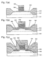
- a gate electrode of an N-type field-effect transistor is conventionally formed by the below-described process using a salicide technique.
- a polysilicon film is deposited on a silicon substrate 301 on which a p-well region 302, a field oxide film 303 and a gate oxide film 304 have been formed, and the polysilicon film is patterned by a reactive ion etching (RIE) method with an etching gas containing a halogen using an etching mask 306 to form a gate electrode 305.
- RIE reactive ion etching
- impurity ions are implanted to be contained in a low concentration in the resulting silicon substrate 301 with intervention of a protective film 307 of silicon oxide against ion implantation to form an LDD (Lightly Doped Drain) region 308.
- LDD Lightly Doped Drain
- a silicon oxide film 309 is deposited on the entire surface of the resulting silicon substrate 301 and as shown in Fig. 7(d), the silicon oxide film 309 is etched back by the RIE method to form a sidewall spacer 310.
- an ion implantation is performed again via a protective film 312 against ion implantation, followed by thermal treatment, to form a source/drain region 313.
- a titanium film 314 is deposited, followed by thermal treatment by an RTA (Rapid Thermal Annealing) method under nitrogen atmosphere to react the titanium film 314 with silicon 301 and 305 to form a titanium silicide film 315.
- RTA Rapid Thermal Annealing
- an unreacted titanium film and a titanium nitride film formed on the surface are selectively removed using a mixture solution of sulfuric acid and aqueous hydrogen peroxide to form titanium silicide electrodes on the source/drain region 308 and the gate electrode 305 in self-alignment.
- the oxide film 309 is over-etched by about 10 to 30 % of the thickness thereof. Therefore, it is also a problem that the surface of the silicon substrate is directly exposed to a halogen-containing etching gas, for example, such as CHF 3 , CF 4 or the like, and thereby that the surface of the silicon substrate is contaminated by halogen atoms in the etching gas.
- a halogen-containing etching gas for example, such as CHF 3 , CF 4 or the like
- Japanese Unexamined Patent Publication No. JP-A-8-115890 proposes a method for removing the spontaneous oxide film by depositing a metal layer, subjecting to thermal treatment to form a silicide layer and removing the silicide layer.
- Japanese Unexamined Patent Publications JP-A-62-94937 and JP-A-8-250463 propose methods for removing the damaged-by-etching layer by forming an oxide film using a sputtering method or by sacrificial oxidation and removing the oxide film.
- an ashing treatment or a washing treatment of the surface of the substrate with an acid or alkaline solution such as a mixture solution of sulfuric acid and aqueous hydrogen peroxide, a mixture solution of hydrochloric acid and aqueous hydrogen peroxide, a mixture solution of ammonia and aqueous hydrogen peroxide or the like.
- the present invention provides a process for fabricating a semiconductor device according to claim 1.
- the process for fabricating a semiconductor device of the present invention comprises removing halogen atoms existing on the surface of a silicon layer and the subsurface thereof so that the concentration of the halogen atoms becomes 100ppm or lower, and forming an electrode on the resulting silicon layer.
- junction leak current value increases as the implanted dose of fluorine is increased, that is, the existence of fluorine deteriorates the junction leak, when fluorine had been implanted into an n + /p junction, then a titanium silicide film was formed and the junction leak current was measured.
- the inventors of the present invention have found it necessary to effectively remove the contaminants existing not only on the surface of the silicon substrate but also in the subsurface of the silicon substrate as a method for solving the above-described conventional problems, and achieved the present invention.
- silicon layers mean layers which are mainly comprised of silicon, including both a silicon substrate itself and silicon films formed as electrodes or wires for connection on the semiconductor substrate. These silicon layers also include any layer comprised of single-crystalline silicon, polycrystalline silicon or amorphous silicon.
- these silicon layers may be unused, unprocessed or untreated layers before forming a semiconductor device or the like, and may also be any silicon substrate or silicon films under a process of fabricating a semiconductor device. That is, these silicon layers may be a silicon substrate or silicon layers on, in or under which a field oxide film, a gate insulating film, a gate electrode, a sidewall spacer, an interlayer insulating film, a contact hole, a wire for connection, a desired circuit such as a transistor or a capacitor and/or the like are formed.
- such silicon layers may include a silicon layer whose surface and subsurface are contaminated with the etching gas or the like used in the RIE method for patterning a gate electrode or for forming a sidewall spacer (for example, CHF 3 , CF 4 , C 2 F 6 , C 3 F 8 , C 4 F 10 , CCl 2 F 2 , CCl 4 , Cl 2 , HBr, CBrF 3 , SF 6 , NF 3 , CClF 3 or the like), a silicon layer contaminated by etching for forming a contact hole which reaches the surface of the silicon layer through an interlayer insulating film formed on the silicon layer, a silicon layer contaminated with the etching gas for removing by etching an insulating film, a conductive film or the like formed on the surface of the silicon layer, a silicon layer contaminated more deeply in its inside by ion implantation for forming an LDD region, a source/drain region or the like on the above-ment
- the surface of a silicon layer and the subsurface thereof mean the surface of a silicon layer and the subsurface thereof in a region where an electrode is to be formed in a later step.
- the subsurface means an inner region of the silicon layer in proximity to the surface, to which a dopant and its accompanying contaminants are ordinarily introduced by etching, ion implantation, thermal treatment or the like performed during the process for fabricating a semiconductor device.
- Halogen atoms mainly mean atoms which are migrated as contaminants in the steps of cleaning, etching and forming a film during the process for fabricating a semiconductor device, including fluorine, chlorine, bromine or the like, for example.
- a titanium film is first formed on the silicon layer at a temperature of the silicon layer not higher than 500°C and then the titanium film is removed.
- the method of forming the titanium film is not particularly limited as long as the temperature of the silicon layer can be kept at or under 500°C.
- a sputtering method, a chemical vapor deposition (CVD) method, a plating method, a vacuum deposition method, an EB method and an MEB method and the like can be used.
- the sputtering method is preferable because the contaminants are effectively incorporated into the titanium film by use of energy at the formation of the titanium film.
- the thickness of the titanium film is not particularly limited as long as the thickness is such that the contaminants can be removed from the surface of a silicon layer and the subsurface thereof.
- the thickness may be about 20 to 100 nm.
- the temperature of the silicon layer is higher than 500°C when the titanium film is formed, silicon in the silicon layer and titanium in the titanium film are silicided and therefore, a titanium silicide layer is formed on the surface and even in the inside of the silicon layer. This is not perferable because, in a later step of removing the titanium film, the silicide layer will also be removed together and a level difference will occur on the surface of the silicon layer.
- the method of removing the titanium film is not particularly limited as long as the contaminants such as halogen atoms or the like are not left or migrated into the surface of a silicon layer and the subsurface thereof after the titanium film is removed.
- Examples of such methods include chemical etching or the like by dipping or the like using an acid or alkali solution such as a mixture solution of sulfuric acid and aqueous hydrogen peroxide, a mixture solution of hydrochloric acid and aqueous hydrogen peroxide, and a mixture solution of ammonia and aqueous hydrogen peroxide or the like.
- treatment with a solution containing hydrofluoric acid is preferably performed after the removal of the titanium film by chemical etching or the like. This treatment with the solution containing hydrofluoric acid can completely eliminate compounds which have been generated by reaction of titanium and silicon due to the substrate temperature and energy from outside such as sputtering energy or the like.
- the contaminants can be effectively removed which would otherwise result in inhibition of silicide formation reaction, a rise in resistance and a decline in heat resistance (facilitation of cohesion) particularly in the case where an electrode will be formed with use of silicide formation reaction in a later step.
- ion implantation may be performed after the titanium film is formed and before the titanium film is removed.
- This ion implantation can facilitate the incorporation of the contaminants existing on the surface of a silicon layer and in the subsurface thereof into the titanium film with energy of the ion implantation.
- ions used for this implantation include ions of Si, N, As, P, Sb, B, Ga, In and the like. Accelerating voltage in the ion implantation is about 20 to 50 keV, and a dose is about 1 ⁇ 10 15 to 1 ⁇ 10 16 cm -2 .
- electrodes are formed on the silicon layer whose surface and subsurface are cleaned.
- the electrodes here mean those which are used as electrodes and interconnection wires, including those formed as parts of interconnection wires such as a contact plug, a barrier metal and the like.
- Materials for the electrodes are not particularly limited as long as they are conductive materials. Such materials include a variety of substances, for example, metals such as Al, Cu, Au, Pt, Ni and Ag, refractory metals such as Ti, Ta, W and Mo, polysilicon, silicides of refractory metals and polysilicon, and polycides of polysilicon and the silicides.
- the silicide may be preferable when used as the source, drain or gate electrode, because it can be formed in self-alignment and has a low resistance, and Al, Cu and W may be preferable when used as the interconnection wires.
- These conductive materials may be formed into a single-layer film or a laminated film.
- the thickness of the electrode at this time is not particularly limited, and for example, the electrode may be about 150 to 400 nm thick when used as the gate electrode.
- the above-described electrode can be formed by a known method such as the sputtering method, CVD method, plating method or the like.
- a two-step thermal treatment may be used wherein a refractory metal film is deposited to a thickness of about 10 to 50 nm on the silicon layer and the first and second thermal treatment are performed thereafter.
- oven annealing and RTA (Rapid Thermal Annealing) can be used.
- RTA Rapid Thermal Annealing
- the RTA method is preferable in view of controlling diffusion of impurities or the like.
- the first thermal treatment may be performed within the temperature range of 400 to 700°C for about 10 to 30 seconds.
- the second thermal treatment may be performed within the temperature range of 800 to 1000°C, preferably at about 850°C, for about 10 to 30 seconds.
- a titanium silicide layer of phase C49 can be formed by the first thermal treatment, and the titanium silicide layer of phase C49 can be turned into a titanium silicide layer of phase C54 which is stoichiometrically stable and of low resistance.
- a process of ion implantation, a process of patterning or the like may be performed optionally after the first thermal treatment and before the second thermal treatment.
- This example shows a method of cleaning a semiconductor substrate whose surface is contaminated with the contaminants, which method is a part of the process for fabricating a semiconductor device.
- a silicon oxide film was formed on a silicon substrate and the silicon oxide film was etched back in such a manner that it is over-etched by about 20 % of the thickness thereof by the RIE method using a mixture gas of CHF 3 , CF 4 and Ar as etching gas to remove the silicon oxide film.
- a titanium film 103 was formed to a thickness of about 30 nm on the silicon substrate 101 by the sputtering method.
- the substrate temperature during the formation of the titanium film 103 was 200°C.
- the persistent contaminants 102 existing on the surface of the silicon substrate 101 and the contaminants 102 existing in the subsurface of the silicon substrate, which cannot be removed by ordinary washing with an acid or alkali solution, can be incorporated into the titanium film 103 which includes a titanium silicide film 104 formed by this reaction.
- the substrate has a relatively low temperature of 500°C or lower, the reaction of silicon atoms on the surface of the silicon substrate 101 with the titanium film 103 is minimized so that the surface of the silicon substrate 101 is not roughened.
- the titanium silicide film 104 left on the surface of the silicon substrate 101 which was a product by the reaction of the titanium film 103 with silicon atoms was removed by chemical etching by being dipped in a 0.5 % aqueous hydrofluoric acid solution at room temperature for about 30 to 45 seconds.
- Atoms on the surface of the silicon substrate 101 are identified in each of the above-described steps by X-ray photoelectron spectroscopy (XPS). The result is shown in Table 1.
- the silicon substrate 101 whose surface 105 was clean and scarcely damaged was obtained.
- the contaminants 102 mainly on the surface and in the subsurface are reacted with the titanium film 103 and then the titanium film 103 is removed, the contaminants 102 can be removed with the titanium film 103, so that the surface of the silicon substrate 101 and the subsurface thereof can be cleaned. Additionally, since thermal treatment to react the titanium film 103 with silicon atoms is not performed, in particular, the surface of the silicon substrate 101 is not damaged during the process.
- This example shows heat resisting characteristics of a titanium silicide film in the case where the titanium silicide film is formed as an electrode on a silicon layer after the surface of the silicon layer and the subsurface thereof are cleaned.
- a p-well region, a field oxide film, a gate oxide film and the like were formed on the silicon substrate, a polysilicon was deposited to have a thickness of about 150 to 200nm on the resulting silicon substrate, then a gate electrode was formed using a mixture gas of HBr, Cl 2 and O 2 as etching gas, and then an LDD region was formed by ion implantation using a protective film against ion implantation (a film of silicon oxide having a thickness of about 10 to 40 nm). This implantation of impurity ions was performed, for example, at an accelerating voltage of 20 keV in a dose of about 1 ⁇ 10 13 to 3 ⁇ 10 14 cm -2 for forming an N-type channel transistor.
- a silicon oxide film was formed on the entire surface of the resulting silicon substrate and the silicon oxide film was etched back to be over-etched about 20 % by the RIE method using a mixture gas of CHF 3 , CF 4 and Ar to form a sidewall spacer on a side wall of the gate electrode.
- ion implantation was performed again to form a source/drain region using a protective film against ion implantation of a silicon oxide film.
- arsenic ions were implanted at an accelerating voltage of about 30 to 60 keV in a dose of about 1 ⁇ 10 15 to 5 ⁇ 10 15 cm -2 , for example, for forming an N-type channel transistor.
- a titanium film was deposited on the resulting silicon substrate to a thickness of 30 nm at a substrate temperature of 200°C or 440°C in the same manner as in Example 1, and then the titanium film was removed by chemical etching by being dipped in a mixture solution of sulfuric acid and hydrogen peroxide (about 5:1 to about 10:1, at 150°C) for about 10 minutes. Subsequently, the titanium silicide film which has been left on the surface of the silicon substrate was removed by chemical etching by being dipped in a 0.5% aqueous hydrofluoric acid solution for about 30 to 45 seconds.
- a titanium film having a thickness of about 30 nm was deposited on the resulting silicon substrate, and silicon ions are implanted at an accelerating voltage of about 40keV in a dose of 5 ⁇ 10 15 cm -2 , for example, for facilitating homogeneous reaction of silicon with titanium.
- a mixture solution of sulfuric acid and hydrogen peroxide about 5:1 to about 10:1, at 150°C
- the sheet resistance of the obtained titanium silicide is shown in Fig.2 (a) to Fig.2 (e).
- sample (2) denotes the case where the titanium film used for cleaning was formed at a substrate temperature of 200°C
- sample (3) denotes the case where the titanium silicide was formed at a substrate temperature of 440°C.
- sample (1) denotes the case where the silicon substrate was subjected to cleaning with the mixture solution of sulfuric acid and hydrogen peroxide but the titanium film was not formed and removed
- sample (4) denotes the case where the titanium silicide film was formed on a clean silicon substrate which had not been subjected to RIE etching.
- the substrate temperature is preferably within the range of 200 to 500°C.
- This example shows variation in sheet resistance with respect to gate length in the case where the titanium silicide film was formed as a gate electrode on a silicon layer whose surface and subsurface have been cleaned.
- the gate electrodes of this example were formed in the same manner as in Example 2 except that the titanium film was formed at a substrate temperature of 440°C and the second thermal treatment was performed at 850°C.
- the gate electrodes were formed to have a gate length within the range of 0.1 to 0.7 ⁇ m.
- each gate electrode is represented by ( ⁇ ) in Fig.3.
- gate electrodes were formed in the same manner as in this example except that the formation and removal of the titanium film were not performed, and the sheet resistance of each gate electrode was also measured. The results are represented by ( ⁇ ).
- the sheet resistance of the gate electrodes formed thereafter was scarcely increased even if the gate length was reduced to as small as 0.1 ⁇ m.
- the gate electrodes were formed in the same manner as in a conventional method wherein the formation and removal of the titanium film were not carried out, the sheet resistance was drastically increased, especially in a fine wire gate having a width of 0.5 ⁇ m or smaller.
- This example shows an example wherein the method of Example 1 is applied to a salicide technique (self-aligned source, drain, gate silicide formation technique).
- a gate oxide film 204 was formed on a silicon substrate 201 having a device isolation film 203 and a well region 202 thereon, a polysilicon was deposited on the resulting silicon substrate 201, a gate electrode 205 was formed using a mixture gas of HBr, Cl 2 and O 2 as etching gas, and ion implantation was performed using a protective film against ion implantation (not shown) to form an LDD region 207.
- a silicon oxide film having a thickness of about 100 to 200 nm was formed on the resulting silicon substrate 201, and the silicon oxide film was etched back by the RIE method using a mixture gas of CHF 3 , CF 1 and Ar as etching gas so as to be over-etched about 20 %, thereby to form a sidewall spacer 206 on a side wall of the gate electrode.
- ion implantation was again performed using a protective film against ion implantation of silicon oxide (not shown) to form a source/drain region 208. Then, the protective film against ion implantation was removed.
- a titanium film 209 was formed to a thickness of 30 nm on the silicon substrate 201 by the sputtering method at a substrate temperature of 440°C.
- the titanium film 209 containing the contaminants was removed by chemical etching using a mixture solution of sulfuric acid and hydrogen peroxide (about 5:1 to 10:1, at 150°C), then the titanium silicide film 210 which remains on the surface of the silicon substrate 201 and contains products by the reaction of titanium with the contaminants was removed by chemical etching by being dipped in a 0.5 % solution of hydrofluoric acid.
- etching time was set to within 90 seconds in order to protect the sidewall spacer 206 formed previously. Since titanium deposited on the surface was also be able to be removed completely by this chemical etching, the contamination of the surface of the silicon substrate 201 and the gate electrode 205 with titanium is eliminated. In addition, there was no possibility that devices which were to be used in later steps would be contaminated by remaining titanium.
- a titanium film 212 of about 30 nm thickness was deposited on the resulting silicon substrate 201, and silicon ions were implanted at an accelerating voltage of 40 keV in a dose of 5 ⁇ 10 15 cm -2 so as to agitate the interfaces of titanium and silicon in view of promoting homogeneous reaction of silicon and titanium.
- a titanium silicide layer 213 of phase C49 was formed by reacting titanium with silicon by the first thermal treatment at about 625°C for about 10 seconds. At this time, in a region where silicon and the titanium film were in contact with each other, silicide formation reaction occurred and the titanium silicide film was formed. On the other hand, in a region where the silicon oxide film and the titanium film were in contact with each other, the silicide formation reaction was inhibited and the titanium silicide film was not formed. Accordingly, subsequently, an unreacted titanium film 212 was removed by wet etching using a mixture solution of sulfuric acid and aqueous hydrogen peroxide. Then, the second thermal treatment was performed at about 875°C for about 10 seconds to turn the titanium silicide layer 213 of phase C49 into the titanium silicide layer of phase C54 having a lower resistance.
- the titanium silicide film 213 was formed on the source/drain region 208 and on the gate electrode 205 in a self-alignment.
- the contaminants on the surface of the silicon substrate 201 and the gate electrode 205 were removed by setting the temperature of the substrate to 500°C or lower when the titanium film 209 was formed.
- the substrate temperature is set to 500°C or higher, for example, 700°C
- titanium is reacted with the silicon substrate 201 and the gate electrode 205 beyond the interfaces and a crystalline silicide is produced.
- the crystalline silicide is etched away simultaneously and level difference 400 appears on the surfaces of the silicon substrate 201 and the gate electrode 205 as shown in Fig.5 (a). Moreover, since titanium is reacted with silicon in a reaction system containing the contaminants, the silicidation reaction does not take place homogeneously as described above. It causes more remarkable level difference 400 on the surfaces of the silicon substrate 201 and the gate electrode 205, and flat surfaces cannot be obtained.
- the titanium silicide film 213 is formed on the silicon substrate 201 and the gate electrode 205 which have the level difference 400 formed thereon, a uniform titanium silicide film 213 is not obtained as shown in Fig.5 (b) and heat resistance degrades, which results in a higher resistance of the titanium silicide film 213. Additionally, since the interface between the finally obtained titanium silicide film 213 and silicon substrate 201 is in a deeper position, the junction of the source/drain region 208 with the well region 202 comes closer to the titanium silicide film 213, which leads to an increase of junction leak current. For preventing this, a shallow junction cannot be formed on the surface of the silicon substrate 201. Therefore, miniaturization of MOSFET will be difficult.
- the formation and removal of the titanium film was carried out after the formation of the source/drain region, the formation and removal of the titanium film may be carried out after the formation of the sidewall spacer and before the formation of the source/ drain region.
- This example shows an example of removing the contaminants still more positively by ion implantation.
- Example 4 In the same manner as in Example 4, mainly, a gate electrode and a sidewall spacer were formed and a titanium film was formed by the sputtering method to a thickness of 30 nm on a silicon substrate. Thereafter, silicon ions were implanted into the silicon substrate and the gate electrode at an accelerating voltage of about 20 to 50 keV in a dose of about 1 ⁇ 10 15 to 1 ⁇ 10 16 , cm -2 through the resulting titanium film.
- the ion implantation after the formation of the titanium film and before the removal of the titanium film can mix the titanium film and the contaminants, the contaminants existing in the subsurface of the silicon substrate can be effectively incorporated into the titanium film by ion implantation energy. Therefore, the removal of the contaminants is reliably done by removing the titanium film and the titanium silicide film.
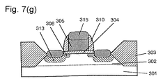
- This example shows an example wherein the method of Example 1 is applied to a process for forming a contact.
- a gate oxide film 304, a gate electrode 305 and a sidewall 310 were formed on a silicon substrate 301 having a device isolation film 303 and a well region 302, then a source/drain region 313 having an LDD region 308 was formed in the subsurface of the silicon substrate 301.
- an interlayer insulating film 501 having a thickness of about 400 nm was formed on the resulting silicon substrate 301, and a contact hole 502 was opened in the interlayer insulating film 501 on the source/drain region 313 by the RIE method using a photoresist mask having a desired configuration (not shown) and C 4 F 8 or the like as an etching gas.
- the surface 503 of the silicon substrate 301 at the bottom of the contact hole was contaminated by halogen atoms contained in the etching gas.
- a titanium film 504 having a thickness of about 30 nm was deposited on the entire surface of the silicon substrate 301 including the contact hole 502 by the sputtering method at 440°C.
- Example 1 the contaminants on the surface 503 of the silicon substrate 301 at the bottom of the contact hole 502 reacted with the deposited titanium film 504 and was incorporated into the titanium film 504 and a titanium silicide film 505 formed by energy at the sputtering.
- a titanium film (not shown) was deposited to a thickness of about 50 to 100 nm in the contact hole by a known method, followed by thermal treatment under nitrogen atmosphere to allow silicon and titanium to react with each other at the bottom of the contact hole 502 and simultaneously form titanium nitride on the surface of the titanium film to produce a barrier metal (not shown). Subsequently, a metal for interconnection was embedded in the contact hole 502 and patterned to form a metal interconnection 507.
- the bottom of the contact hole which is contaminated by the etching gas for opening the contact hole can be cleaned.
- the resistance of the contact can be reduced.
- An ohmic property of the contact hole is deteriorated by a slight contamination as an opening area of the contact and a contact area of the source/drain region with the metal interconnection become smaller.
- the method of this example is more effective especially as the opening area of the contact becomes smaller.
- the concentration of halogen atoms on existing the surface of the silicon layer and in the subsurface thereof is reduced to 100ppm or lower.
- the heat resistance of the obtained electrode can be improved and the resistance of the electrode can be reduced.
- the method for reducing the concentration of halogen atoms existing on the surface of the silicon substrate and in the subsurface thereof to 100ppm or lower comprises forming a titanium film at a temperature of the silicon layer of 500°C or lower and removing the titanium film, the contaminants adhering to the surface of the silicon layer and the subsurface thereof can be incorporated into the titanium film with use of the readiness of titanium to react with other substances (high reducing ability).
- the removal of the titanium film the contaminants which would otherwise produce problems in later steps are reliably removed and, the surface of the silicon layer and the subsurface thereof can be cleaned.
- a contact having a greater ohmic property can be formed at the interface between the electrode and the silicon layer.
- the titanium film is formed under the condition of a moderate temperature of the silicon layer of 500°C or lower, damage to the surface of the silicon layer can be prevented to the utmost when the titanium film is removed. Consequently, when an electrode is formed on the silicon layer in a later step, it is possible not only to prevent deterioration of an ohmic contact which would result from the damage of the surface of the silicon layer, but also to improve the uniformity of the film of the electrode and the resistance and heat resistance of the electrode, and further, to prevent the leak current.
Landscapes
- Engineering & Computer Science (AREA)
- Microelectronics & Electronic Packaging (AREA)
- Condensed Matter Physics & Semiconductors (AREA)
- General Physics & Mathematics (AREA)
- Manufacturing & Machinery (AREA)
- Computer Hardware Design (AREA)
- Physics & Mathematics (AREA)
- Power Engineering (AREA)
- Chemical & Material Sciences (AREA)
- Chemical Kinetics & Catalysis (AREA)
- Electrodes Of Semiconductors (AREA)
- Insulated Gate Type Field-Effect Transistor (AREA)
- Internal Circuitry In Semiconductor Integrated Circuit Devices (AREA)
Applications Claiming Priority (3)
| Application Number | Priority Date | Filing Date | Title |
|---|---|---|---|
| JP10867197 | 1997-04-25 | ||
| JP10867197A JP4101901B2 (ja) | 1997-04-25 | 1997-04-25 | 半導体装置の製造方法 |
| PCT/JP1998/001892 WO1998049724A1 (fr) | 1997-04-25 | 1998-04-23 | Procede de fabrication de dispositif a semi-conducteurs |
Publications (3)
| Publication Number | Publication Date |
|---|---|
| EP0928021A1 EP0928021A1 (en) | 1999-07-07 |
| EP0928021A4 EP0928021A4 (en) | 2000-12-06 |
| EP0928021B1 true EP0928021B1 (en) | 2007-06-13 |
Family
ID=14490735
Family Applications (1)
| Application Number | Title | Priority Date | Filing Date |
|---|---|---|---|
| EP98917666A Expired - Lifetime EP0928021B1 (en) | 1997-04-25 | 1998-04-23 | Process for manufacturing semiconductor device |
Country Status (6)
| Country | Link |
|---|---|
| US (2) | US6562699B1 (enExample) |
| EP (1) | EP0928021B1 (enExample) |
| JP (1) | JP4101901B2 (enExample) |
| KR (1) | KR100399492B1 (enExample) |
| DE (1) | DE69837909T2 (enExample) |
| WO (1) | WO1998049724A1 (enExample) |
Families Citing this family (8)
| Publication number | Priority date | Publication date | Assignee | Title |
|---|---|---|---|---|
| JP4101901B2 (ja) * | 1997-04-25 | 2008-06-18 | シャープ株式会社 | 半導体装置の製造方法 |
| GB2360292B (en) * | 2000-03-15 | 2002-04-03 | Murata Manufacturing Co | Photosensitive thick film composition and electronic device using the same |
| US7721491B2 (en) * | 2004-07-23 | 2010-05-25 | Jennifer Appel | Method and system for storing water inside buildings |
| US20060057853A1 (en) * | 2004-09-15 | 2006-03-16 | Manoj Mehrotra | Thermal oxidation for improved silicide formation |
| TW200816312A (en) * | 2006-09-28 | 2008-04-01 | Promos Technologies Inc | Method for forming silicide layer on a silicon surface and its use |
| JP5076557B2 (ja) * | 2007-03-06 | 2012-11-21 | 富士通セミコンダクター株式会社 | 半導体装置の製造方法 |
| US10446662B2 (en) | 2016-10-07 | 2019-10-15 | Taiwan Semiconductor Manufacturing Co., Ltd. | Reducing metal gate overhang by forming a top-wide bottom-narrow dummy gate electrode |
| US10510851B2 (en) * | 2016-11-29 | 2019-12-17 | Taiwan Semiconductor Manufacturing Company, Ltd. | Low resistance contact method and structure |
Family Cites Families (24)
| Publication number | Priority date | Publication date | Assignee | Title |
|---|---|---|---|---|
| JP3095564B2 (ja) * | 1992-05-29 | 2000-10-03 | 株式会社東芝 | 半導体装置及び半導体装置の製造方法 |
| US3601666A (en) * | 1969-08-21 | 1971-08-24 | Texas Instruments Inc | Titanium tungsten-gold contacts for semiconductor devices |
| US4629611A (en) * | 1985-04-29 | 1986-12-16 | International Business Machines Corporation | Gas purifier for rare-gas fluoride lasers |
| JPS61258434A (ja) | 1985-05-13 | 1986-11-15 | Nec Corp | 半導体装置の製造方法 |
| JPH0682641B2 (ja) | 1985-10-21 | 1994-10-19 | 日本電気株式会社 | 半導体集積回路装置の製造方法 |
| US4690730A (en) * | 1986-03-07 | 1987-09-01 | Texas Instruments Incorporated | Oxide-capped titanium silicide formation |
| US4981550A (en) * | 1987-09-25 | 1991-01-01 | At&T Bell Laboratories | Semiconductor device having tungsten plugs |
| US4851358A (en) * | 1988-02-11 | 1989-07-25 | Dns Electronic Materials, Inc. | Semiconductor wafer fabrication with improved control of internal gettering sites using rapid thermal annealing |
| US4981816A (en) * | 1988-10-27 | 1991-01-01 | General Electric Company | MO/TI Contact to silicon |
| US5084417A (en) * | 1989-01-06 | 1992-01-28 | International Business Machines Corporation | Method for selective deposition of refractory metals on silicon substrates and device formed thereby |
| JP2660359B2 (ja) * | 1991-01-30 | 1997-10-08 | 三菱電機株式会社 | 半導体装置 |
| KR970009867B1 (ko) * | 1993-12-17 | 1997-06-18 | 현대전자산업 주식회사 | 반도체 소자의 텅스텐 실리사이드 형성방법 |
| JPH08115890A (ja) | 1994-10-17 | 1996-05-07 | Fujitsu Ltd | 半導体基板上への電極形成方法 |
| JP2630290B2 (ja) * | 1995-01-30 | 1997-07-16 | 日本電気株式会社 | 半導体装置の製造方法 |
| JPH08213343A (ja) * | 1995-01-31 | 1996-08-20 | Sony Corp | 半導体装置およびその製造方法 |
| JPH08250463A (ja) | 1995-03-07 | 1996-09-27 | Nippon Steel Corp | 半導体装置の製造方法 |
| US5972790A (en) * | 1995-06-09 | 1999-10-26 | Tokyo Electron Limited | Method for forming salicides |
| US5595784A (en) * | 1995-08-01 | 1997-01-21 | Kaim; Robert | Titanium nitride and multilayers formed by chemical vapor deposition of titanium halides |
| US5830802A (en) * | 1995-08-31 | 1998-11-03 | Motorola Inc. | Process for reducing halogen concentration in a material layer during semiconductor device fabrication |
| EP0793271A3 (en) * | 1996-02-22 | 1998-12-02 | Matsushita Electric Industrial Co., Ltd. | Semiconductor device having a metal silicide film and method of fabricating the same |
| JPH09320990A (ja) * | 1996-03-25 | 1997-12-12 | Sharp Corp | 半導体装置の製造方法 |
| US5963828A (en) * | 1996-12-23 | 1999-10-05 | Lsi Logic Corporation | Method for tungsten nucleation from WF6 using titanium as a reducing agent |
| JP4101901B2 (ja) * | 1997-04-25 | 2008-06-18 | シャープ株式会社 | 半導体装置の製造方法 |
| KR19990041688A (ko) * | 1997-11-24 | 1999-06-15 | 김규현 | 티타늄 샐리사이드 형성 방법 |
-
1997
- 1997-04-25 JP JP10867197A patent/JP4101901B2/ja not_active Expired - Fee Related
-
1998
- 1998-04-23 DE DE69837909T patent/DE69837909T2/de not_active Expired - Lifetime
- 1998-04-23 WO PCT/JP1998/001892 patent/WO1998049724A1/ja not_active Ceased
- 1998-04-23 EP EP98917666A patent/EP0928021B1/en not_active Expired - Lifetime
- 1998-04-23 US US09/202,714 patent/US6562699B1/en not_active Expired - Fee Related
- 1998-04-23 KR KR10-1998-0710275A patent/KR100399492B1/ko not_active Expired - Fee Related
-
2003
- 2003-03-24 US US10/394,024 patent/US7135386B2/en not_active Expired - Fee Related
Also Published As
| Publication number | Publication date |
|---|---|
| DE69837909D1 (de) | 2007-07-26 |
| EP0928021A1 (en) | 1999-07-07 |
| US6562699B1 (en) | 2003-05-13 |
| US20030170967A1 (en) | 2003-09-11 |
| JP4101901B2 (ja) | 2008-06-18 |
| KR100399492B1 (ko) | 2003-12-24 |
| KR20000016675A (ko) | 2000-03-25 |
| WO1998049724A1 (fr) | 1998-11-05 |
| DE69837909T2 (de) | 2008-02-14 |
| EP0928021A4 (en) | 2000-12-06 |
| JPH10303145A (ja) | 1998-11-13 |
| US7135386B2 (en) | 2006-11-14 |
Similar Documents
| Publication | Publication Date | Title |
|---|---|---|
| US6255702B1 (en) | Semiconductor device having junction depths for reducing short channel effect | |
| US6436747B1 (en) | Method of fabricating semiconductor device | |
| KR100530401B1 (ko) | 저저항 게이트 전극을 구비하는 반도체 장치 | |
| US6784506B2 (en) | Silicide process using high K-dielectrics | |
| US6720627B1 (en) | Semiconductor device having junction depths for reducing short channel effect | |
| EP0750338A2 (en) | Etching process of CoSi2 layers | |
| US6083815A (en) | Method of gate etching with thin gate oxide | |
| EP0928021B1 (en) | Process for manufacturing semiconductor device | |
| US20020004303A1 (en) | Wet cleans for cobalt disilicide processing | |
| US20020025676A1 (en) | Salicide formation process | |
| WO2007037881A2 (en) | Semiconductor fabrication process including silicide stringer removal processing | |
| US7448395B2 (en) | Process method to facilitate silicidation | |
| JPH11204492A (ja) | 半導体装置の製造方法 | |
| JPH0982812A (ja) | 半導体装置の製造方法 | |
| KR100628225B1 (ko) | 반도체 소자의 제조방법 | |
| JP2833530B2 (ja) | 半導体装置の製造方法 | |
| JPH08339970A (ja) | 半導体装置及びその製造方法 | |
| JPH0611074B2 (ja) | 半導体装置の製造方法 | |
| US6777300B2 (en) | Method to improve silicide formation on polysilicon | |
| US6472311B1 (en) | Method for manufacturing semiconductor device | |
| JPH1154455A (ja) | 半導体装置の製造方法 | |
| US7572719B2 (en) | Semiconductor device and manufacturing method thereof | |
| KR100291276B1 (ko) | 반도체 소자의 실리사이드 형성 방법 | |
| US20010052626A1 (en) | Method for fabricating dual-gate structure | |
| JPH10223560A (ja) | 半導体装置及びその製造方法 |
Legal Events
| Date | Code | Title | Description |
|---|---|---|---|
| PUAI | Public reference made under article 153(3) epc to a published international application that has entered the european phase |
Free format text: ORIGINAL CODE: 0009012 |
|
| 17P | Request for examination filed |
Effective date: 19990316 |
|
| AK | Designated contracting states |
Kind code of ref document: A1 Designated state(s): DE FR GB |
|
| A4 | Supplementary search report drawn up and despatched |
Effective date: 20001019 |
|
| AK | Designated contracting states |
Kind code of ref document: A4 Designated state(s): DE FR GB |
|
| RIC1 | Information provided on ipc code assigned before grant |
Free format text: 7H 01L 21/336 A, 7H 01L 29/78 B, 7H 01L 21/28 B, 7H 01L 21/285 B |
|
| 17Q | First examination report despatched |
Effective date: 20020607 |
|
| GRAP | Despatch of communication of intention to grant a patent |
Free format text: ORIGINAL CODE: EPIDOSNIGR1 |
|
| GRAS | Grant fee paid |
Free format text: ORIGINAL CODE: EPIDOSNIGR3 |
|
| GRAA | (expected) grant |
Free format text: ORIGINAL CODE: 0009210 |
|
| RAP1 | Party data changed (applicant data changed or rights of an application transferred) |
Owner name: SHARP KABUSHIKI KAISHA |
|
| AK | Designated contracting states |
Kind code of ref document: B1 Designated state(s): DE FR GB |
|
| REG | Reference to a national code |
Ref country code: GB Ref legal event code: FG4D |
|
| REF | Corresponds to: |
Ref document number: 69837909 Country of ref document: DE Date of ref document: 20070726 Kind code of ref document: P |
|
| ET | Fr: translation filed | ||
| PLBE | No opposition filed within time limit |
Free format text: ORIGINAL CODE: 0009261 |
|
| STAA | Information on the status of an ep patent application or granted ep patent |
Free format text: STATUS: NO OPPOSITION FILED WITHIN TIME LIMIT |
|
| 26N | No opposition filed |
Effective date: 20080314 |
|
| PGFP | Annual fee paid to national office [announced via postgrant information from national office to epo] |
Ref country code: GB Payment date: 20130417 Year of fee payment: 16 Ref country code: DE Payment date: 20130508 Year of fee payment: 16 |
|
| PGFP | Annual fee paid to national office [announced via postgrant information from national office to epo] |
Ref country code: FR Payment date: 20130625 Year of fee payment: 16 |
|
| REG | Reference to a national code |
Ref country code: DE Ref legal event code: R119 Ref document number: 69837909 Country of ref document: DE |
|
| GBPC | Gb: european patent ceased through non-payment of renewal fee |
Effective date: 20140423 |
|
| REG | Reference to a national code |
Ref country code: DE Ref legal event code: R119 Ref document number: 69837909 Country of ref document: DE Effective date: 20141101 |
|
| REG | Reference to a national code |
Ref country code: FR Ref legal event code: ST Effective date: 20141231 |
|
| PG25 | Lapsed in a contracting state [announced via postgrant information from national office to epo] |
Ref country code: GB Free format text: LAPSE BECAUSE OF NON-PAYMENT OF DUE FEES Effective date: 20140423 Ref country code: DE Free format text: LAPSE BECAUSE OF NON-PAYMENT OF DUE FEES Effective date: 20141101 |
|
| PG25 | Lapsed in a contracting state [announced via postgrant information from national office to epo] |
Ref country code: FR Free format text: LAPSE BECAUSE OF NON-PAYMENT OF DUE FEES Effective date: 20140430 |