EP0902471B1 - Integrierte Halbleiterschaltungsanordnung und Packungstruktur dafür - Google Patents
Integrierte Halbleiterschaltungsanordnung und Packungstruktur dafür Download PDFInfo
- Publication number
- EP0902471B1 EP0902471B1 EP98306868A EP98306868A EP0902471B1 EP 0902471 B1 EP0902471 B1 EP 0902471B1 EP 98306868 A EP98306868 A EP 98306868A EP 98306868 A EP98306868 A EP 98306868A EP 0902471 B1 EP0902471 B1 EP 0902471B1
- Authority
- EP
- European Patent Office
- Prior art keywords
- electrode
- electrodes
- signal
- power supply
- chip
- Prior art date
- Legal status (The legal status is an assumption and is not a legal conclusion. Google has not performed a legal analysis and makes no representation as to the accuracy of the status listed.)
- Expired - Lifetime
Links
Images


Classifications
-
- H—ELECTRICITY
- H10—SEMICONDUCTOR DEVICES; ELECTRIC SOLID-STATE DEVICES NOT OTHERWISE PROVIDED FOR
- H10W—GENERIC PACKAGES, INTERCONNECTIONS, CONNECTORS OR OTHER CONSTRUCTIONAL DETAILS OF DEVICES COVERED BY CLASS H10
- H10W42/00—Arrangements for protection of devices
- H10W42/20—Arrangements for protection of devices protecting against electromagnetic or particle radiation, e.g. light, X-rays, gamma-rays or electrons
-
- H—ELECTRICITY
- H10—SEMICONDUCTOR DEVICES; ELECTRIC SOLID-STATE DEVICES NOT OTHERWISE PROVIDED FOR
- H10W—GENERIC PACKAGES, INTERCONNECTIONS, CONNECTORS OR OTHER CONSTRUCTIONAL DETAILS OF DEVICES COVERED BY CLASS H10
- H10W72/00—Interconnections or connectors in packages
-
- H—ELECTRICITY
- H10—SEMICONDUCTOR DEVICES; ELECTRIC SOLID-STATE DEVICES NOT OTHERWISE PROVIDED FOR
- H10W—GENERIC PACKAGES, INTERCONNECTIONS, CONNECTORS OR OTHER CONSTRUCTIONAL DETAILS OF DEVICES COVERED BY CLASS H10
- H10W72/00—Interconnections or connectors in packages
- H10W72/50—Bond wires
-
- H—ELECTRICITY
- H10—SEMICONDUCTOR DEVICES; ELECTRIC SOLID-STATE DEVICES NOT OTHERWISE PROVIDED FOR
- H10W—GENERIC PACKAGES, INTERCONNECTIONS, CONNECTORS OR OTHER CONSTRUCTIONAL DETAILS OF DEVICES COVERED BY CLASS H10
- H10W72/00—Interconnections or connectors in packages
- H10W72/90—Bond pads, in general
-
- H—ELECTRICITY
- H10—SEMICONDUCTOR DEVICES; ELECTRIC SOLID-STATE DEVICES NOT OTHERWISE PROVIDED FOR
- H10W—GENERIC PACKAGES, INTERCONNECTIONS, CONNECTORS OR OTHER CONSTRUCTIONAL DETAILS OF DEVICES COVERED BY CLASS H10
- H10W44/00—Electrical arrangements for controlling or matching impedance
- H10W44/20—Electrical arrangements for controlling or matching impedance at high-frequency [HF] or radio frequency [RF]
- H10W44/203—Electrical connections
- H10W44/206—Wires
-
- H—ELECTRICITY
- H10—SEMICONDUCTOR DEVICES; ELECTRIC SOLID-STATE DEVICES NOT OTHERWISE PROVIDED FOR
- H10W—GENERIC PACKAGES, INTERCONNECTIONS, CONNECTORS OR OTHER CONSTRUCTIONAL DETAILS OF DEVICES COVERED BY CLASS H10
- H10W70/00—Package substrates; Interposers; Redistribution layers [RDL]
- H10W70/60—Insulating or insulated package substrates; Interposers; Redistribution layers
- H10W70/67—Insulating or insulated package substrates; Interposers; Redistribution layers characterised by their insulating layers or insulating parts
- H10W70/68—Shapes or dispositions thereof
- H10W70/682—Shapes or dispositions thereof comprising holes having chips therein
-
- H—ELECTRICITY
- H10—SEMICONDUCTOR DEVICES; ELECTRIC SOLID-STATE DEVICES NOT OTHERWISE PROVIDED FOR
- H10W—GENERIC PACKAGES, INTERCONNECTIONS, CONNECTORS OR OTHER CONSTRUCTIONAL DETAILS OF DEVICES COVERED BY CLASS H10
- H10W72/00—Interconnections or connectors in packages
- H10W72/071—Connecting or disconnecting
- H10W72/075—Connecting or disconnecting of bond wires
- H10W72/07531—Techniques
- H10W72/07532—Compression bonding, e.g. thermocompression bonding
- H10W72/07533—Ultrasonic bonding, e.g. thermosonic bonding
-
- H—ELECTRICITY
- H10—SEMICONDUCTOR DEVICES; ELECTRIC SOLID-STATE DEVICES NOT OTHERWISE PROVIDED FOR
- H10W—GENERIC PACKAGES, INTERCONNECTIONS, CONNECTORS OR OTHER CONSTRUCTIONAL DETAILS OF DEVICES COVERED BY CLASS H10
- H10W72/00—Interconnections or connectors in packages
- H10W72/071—Connecting or disconnecting
- H10W72/075—Connecting or disconnecting of bond wires
- H10W72/07551—Connecting or disconnecting of bond wires characterised by changes in properties of the bond wires during the connecting
- H10W72/07554—Connecting or disconnecting of bond wires characterised by changes in properties of the bond wires during the connecting changes in dispositions
-
- H—ELECTRICITY
- H10—SEMICONDUCTOR DEVICES; ELECTRIC SOLID-STATE DEVICES NOT OTHERWISE PROVIDED FOR
- H10W—GENERIC PACKAGES, INTERCONNECTIONS, CONNECTORS OR OTHER CONSTRUCTIONAL DETAILS OF DEVICES COVERED BY CLASS H10
- H10W72/00—Interconnections or connectors in packages
- H10W72/50—Bond wires
- H10W72/531—Shapes of wire connectors
- H10W72/536—Shapes of wire connectors the connected ends being ball-shaped
-
- H—ELECTRICITY
- H10—SEMICONDUCTOR DEVICES; ELECTRIC SOLID-STATE DEVICES NOT OTHERWISE PROVIDED FOR
- H10W—GENERIC PACKAGES, INTERCONNECTIONS, CONNECTORS OR OTHER CONSTRUCTIONAL DETAILS OF DEVICES COVERED BY CLASS H10
- H10W72/00—Interconnections or connectors in packages
- H10W72/50—Bond wires
- H10W72/531—Shapes of wire connectors
- H10W72/5363—Shapes of wire connectors the connected ends being wedge-shaped
-
- H—ELECTRICITY
- H10—SEMICONDUCTOR DEVICES; ELECTRIC SOLID-STATE DEVICES NOT OTHERWISE PROVIDED FOR
- H10W—GENERIC PACKAGES, INTERCONNECTIONS, CONNECTORS OR OTHER CONSTRUCTIONAL DETAILS OF DEVICES COVERED BY CLASS H10
- H10W72/00—Interconnections or connectors in packages
- H10W72/50—Bond wires
- H10W72/541—Dispositions of bond wires
- H10W72/5445—Dispositions of bond wires being orthogonal to a side surface of the chip, e.g. parallel arrangements
-
- H—ELECTRICITY
- H10—SEMICONDUCTOR DEVICES; ELECTRIC SOLID-STATE DEVICES NOT OTHERWISE PROVIDED FOR
- H10W—GENERIC PACKAGES, INTERCONNECTIONS, CONNECTORS OR OTHER CONSTRUCTIONAL DETAILS OF DEVICES COVERED BY CLASS H10
- H10W72/00—Interconnections or connectors in packages
- H10W72/50—Bond wires
- H10W72/541—Dispositions of bond wires
- H10W72/547—Dispositions of multiple bond wires
-
- H—ELECTRICITY
- H10—SEMICONDUCTOR DEVICES; ELECTRIC SOLID-STATE DEVICES NOT OTHERWISE PROVIDED FOR
- H10W—GENERIC PACKAGES, INTERCONNECTIONS, CONNECTORS OR OTHER CONSTRUCTIONAL DETAILS OF DEVICES COVERED BY CLASS H10
- H10W72/00—Interconnections or connectors in packages
- H10W72/50—Bond wires
- H10W72/59—Bond pads specially adapted therefor
-
- H—ELECTRICITY
- H10—SEMICONDUCTOR DEVICES; ELECTRIC SOLID-STATE DEVICES NOT OTHERWISE PROVIDED FOR
- H10W—GENERIC PACKAGES, INTERCONNECTIONS, CONNECTORS OR OTHER CONSTRUCTIONAL DETAILS OF DEVICES COVERED BY CLASS H10
- H10W72/00—Interconnections or connectors in packages
- H10W72/90—Bond pads, in general
- H10W72/931—Shapes of bond pads
- H10W72/932—Plan-view shape, i.e. in top view
-
- H—ELECTRICITY
- H10—SEMICONDUCTOR DEVICES; ELECTRIC SOLID-STATE DEVICES NOT OTHERWISE PROVIDED FOR
- H10W—GENERIC PACKAGES, INTERCONNECTIONS, CONNECTORS OR OTHER CONSTRUCTIONAL DETAILS OF DEVICES COVERED BY CLASS H10
- H10W72/00—Interconnections or connectors in packages
- H10W72/90—Bond pads, in general
- H10W72/931—Shapes of bond pads
- H10W72/934—Cross-sectional shape, i.e. in side view
-
- H—ELECTRICITY
- H10—SEMICONDUCTOR DEVICES; ELECTRIC SOLID-STATE DEVICES NOT OTHERWISE PROVIDED FOR
- H10W—GENERIC PACKAGES, INTERCONNECTIONS, CONNECTORS OR OTHER CONSTRUCTIONAL DETAILS OF DEVICES COVERED BY CLASS H10
- H10W72/00—Interconnections or connectors in packages
- H10W72/90—Bond pads, in general
- H10W72/941—Dispositions of bond pads
- H10W72/944—Dispositions of multiple bond pads
- H10W72/9445—Top-view layouts, e.g. mirror arrays
-
- H—ELECTRICITY
- H10—SEMICONDUCTOR DEVICES; ELECTRIC SOLID-STATE DEVICES NOT OTHERWISE PROVIDED FOR
- H10W—GENERIC PACKAGES, INTERCONNECTIONS, CONNECTORS OR OTHER CONSTRUCTIONAL DETAILS OF DEVICES COVERED BY CLASS H10
- H10W72/00—Interconnections or connectors in packages
- H10W72/90—Bond pads, in general
- H10W72/951—Materials of bond pads
-
- H—ELECTRICITY
- H10—SEMICONDUCTOR DEVICES; ELECTRIC SOLID-STATE DEVICES NOT OTHERWISE PROVIDED FOR
- H10W—GENERIC PACKAGES, INTERCONNECTIONS, CONNECTORS OR OTHER CONSTRUCTIONAL DETAILS OF DEVICES COVERED BY CLASS H10
- H10W90/00—Package configurations
- H10W90/701—Package configurations characterised by the relative positions of pads or connectors relative to package parts
- H10W90/721—Package configurations characterised by the relative positions of pads or connectors relative to package parts of bump connectors
- H10W90/722—Package configurations characterised by the relative positions of pads or connectors relative to package parts of bump connectors between stacked chips
-
- H—ELECTRICITY
- H10—SEMICONDUCTOR DEVICES; ELECTRIC SOLID-STATE DEVICES NOT OTHERWISE PROVIDED FOR
- H10W—GENERIC PACKAGES, INTERCONNECTIONS, CONNECTORS OR OTHER CONSTRUCTIONAL DETAILS OF DEVICES COVERED BY CLASS H10
- H10W90/00—Package configurations
- H10W90/701—Package configurations characterised by the relative positions of pads or connectors relative to package parts
- H10W90/751—Package configurations characterised by the relative positions of pads or connectors relative to package parts of bond wires
- H10W90/754—Package configurations characterised by the relative positions of pads or connectors relative to package parts of bond wires between a chip and a stacked insulating package substrate, interposer or RDL
Definitions
- the present invention relates to a semiconductor integrated circuit device and a package structure therefor.
- Fig. 8 illustrates an appearance of a typical chip pattern used for a gate array or the like.
- a circuit portion (active area) 20 is formed in the center part of the chip and a plurality of electrodes 21 are lined up at a predetermined pitch P along the periphery of the chip.
- the circuit portion (active area) 20 is formed as a set of a plurality of individual circuit portions 22 (referred to as 'unit cell' hereinafter).
- the electrode 21 is provided such that it makes one-to-one correspondence with the unit cell 22.
- Fig. 9 is a conceptual illustration showing the basic design of each electrode.
- the electrode 21 is disposed such that it can be individually connected with a power source terminal (P), a ground terminal (G), and a signal input/output (I/O) terminal of a corresponding unit cell 22, through an electrode wiring 23, a ground wiring 24, and a signal I/O wiring 25, respectively.
- P power source terminal
- G ground terminal
- I/O signal input/output
- each of electrodes 21 can optionally use any one of the power source terminal (P), the ground terminal (G), and the signal I/O terminal, depending on a given request. Therefore, this basic wiring design is able to remarkably increase the degree of freedom in the IC design work.
- the basic design of the entire chip can be achieved by first making a basic design unit including a unit cell and electrodes therefor, then duplicating the basic design unit by the necessary number of it, and finally, disposing those which are duplicated.
- the wafer mask is formed so as to have a multi-layer structure, that is, it consists of a common mask for use in formation of the circuit portion, and a mask for use in formation of a wiring layer.
- a multi-layer structure that is, it consists of a common mask for use in formation of the circuit portion, and a mask for use in formation of a wiring layer.
- this can be complied with by just altering some of wiring layer masks.
- a variety of masks are prepared, for instance, one having a wiring pattern in which a certain electrode is connected only with the I/O terminal but with nothing else, and the other having a wiring pattern in which a certain electrode is connected only with the power terminal but with nothing else.
- a chip can be completed through the wafer process as mentioned above. Accordingly, if the chip is manufactured through the above-mentioned manufacturing process, days spent for manufacturing the chip can be effectively shortened, because its basic design is already available as mentioned above and what to be done is to only prepare the masks which meet the client'
- the pitch P of disposing electrodes considerably depends on the technical level on how to connect the electrode with the unit cell. If electrode connection is carried out by a wire bonding method, for instance the most widely used thermosonic wire bonding method, the possible minimum pitch is in a range of 100 to 80 ⁇ m, so that the circuit portion can not help being designed by taking account of this available pitch range. Recently, however, it has become possible to design a circuit portion (active area) with a microminiature size, owing to remarkable progress in the microminiaturization and multilevel interconnection technology adaptable to the wafer process. On the other hand, however, it is the true present state that the technology of electrode connection has not caught up with this microminiaturization technology as yet.
- the known arrangement of electrodes 31 (31a, 31b) in a zigzag fashion as shown in Fig. 10 is one of countermeasures as devised in order to increase the number of electrodes to be disposed on a chip.
- the pitch between the outer electrode 31a and the inner electrode 31b can be made P/2, so that the chip size can be made smaller as a result.
- a reference numeral 30 designates the circuit portion (active area) and 32 does the unit cell.
- Fig. 11 is a conceptual illustration for explaining the basic design of the electrode arrangement in a zigzag fashion. Similar to the wiring arrangement as shown in Fig. 9 , the electrode 31 is disposed such that it can be individually connected with a power source terminal (P), a ground terminal (G), and a signal input/output (I/O) terminal of the unit cell 32 corresponding to the electrode 31, through an electrode wiring 33, a ground wiring 34, and a signal I/O wiring 35, respectively. Therefore, it again becomes possible in this zigzag electrode arrangement that each electrode can be optionally assigned to power supply use, grounding, or the signal I/O.
- P power source terminal
- G ground terminal
- I/O signal input/output
- this zigzag electrode arrangement can contribute to reduction of the chip size, because this electrode arrangement allows the chip to accommodate a large number of electrodes which are inevitable for operation of the circuit portion, even if they are not allowed to be disposed in a single line along the periphery of the chip.
- Fig. 12 is a schematic plan view of a wiring portion while Fig. 13 is a schematic cross sectional view of the wiring portion as shown in Fig. 12 .
- each of electrodes may be optionally used as either a signal I/O electrode, a power supply electrode, or a ground electrode, assignment of them is determined according to a given individual request. For instance, therefore, complying with the request, the signal I/O electrode 42a is connected with the inner lead 43 through a wiring 47a, the power supply electrode 42b is connected with the common power supply ring 44 through a wiring 47b, and the ground electrode 42c is connected with the common ground ring 45 through a wiring 47c. In this way, the wire bonding process is completed when necessary wirings are over.
- the number of electrodes for use in power supply and/or ground would have to be further increased taking account of a countermeasure against noise. Otherwise, the number of electrodes for signal I/O use can not help being relatively decreased. Accordingly, in order to secure the necessary number of signal I/O electrodes, the chip has to be further made larger in its size. As mentioned above, this is against miniaturization of the chip and causes the rise in the manufacturing cost.
- the chip In order to avoid noise interference, it is well known to shield the signal I/O electrode. In this case, shielding is achieved by putting the signal I/O electrode between the power supply electrode and the ground electrode. According to this method, however, in order to satisfy the demand, the chip has to be selected so as to include the number of electrodes larger than the necessary number of signal I/O electrodes. As a matter of course, this causes another increase in chip size against miniaturization thereof, and causes the rise in the manufacturing cost after all.
- the prior art electrode arrangement in the IC device can no longer comply with the demand relating to the number and pitch of electrodes capable of completely satisfying all the functions of the microminiaturized circuit portion, which has been achieved through the recent remarkable progress in the wafer process technology, especially in microminiaturization of the circuit portion with the help of the multi-layer structure. Even the zigzag electrode arrangement still fails to use all the functions obtainable from the circuit portion, rather causing the rise in the manufacturing cost as described above.
- the wiring 47c serves for connecting the electrode 42c with the common power supply ring 45 (or the common ground ring 44).
- the electrode 42c is located inward far from the chip edge 41a while the power supply ring 45 takes a lower position near the chip, the height of the wiring 47c is apt to become lower if it is formed according to the ordinary wire bonding process. Therefore, there might be caused such a risky state that the wiring 47c gets in touch with the chip edge 41a. In order to avoid this risky state, it would be required to take some action such as keeping the wiring 47c away from the edge 41a, for instance rising the height of the wiring 47 like the wiring 47c' as shown on the right side of Fig. 13 . This would require special control or modification of the wire bonding process, which would result in another rise in the manufacturing cost.
- JP9064232 discloses a semiconductor device in accordance with the precharacterising portion of the appended claims, i.e an IC device provided with a chip in which a signal I/0 wiring is located between power supply and ground wirings, thereby being well protected from noise such as crosstalk, and which can run well at a very high operating frequency.
- the IC device is fabricated in a package having a multi-layer structure by means of a stable and reliable ordinary bonding process without need of any special wiring control.
- an object of the invention is to provide a novel and improved IC device wherein the circuit portion (action area) of the chip can be made full use of without increasing the number of electrodes, thereby enabling the chip size to be made relatively smaller and realizing cost reduction in the IC device manufacture.
- the present invention provides a semiconductor IC device comprising:
- the invention may still further provide an IC device wherein a signal I/O wiring for connecting the signal I/O terminal with the signal I/O electrode is made to locate between a power supply wiring for connecting the power supply terminal with the power supply electrode and a ground wiring for connecting the ground terminal with the ground electrode.
- a signal I/O wiring for connecting the signal I/O terminal with the signal I/O electrode is made to locate between a power supply wiring for connecting the power supply terminal with the power supply electrode and a ground wiring for connecting the ground terminal with the ground electrode.
- the above first row on which signal I/O electrodes are disposed is located to be a little near to the active area than the second row on which power supply electrodes and ground electrodes are alternately disposed.
- This package has a multi-layer structure with at least two layers, on the first layer of which a common power supply ring and a common ground ring are disposed, and on the second layer of which a signal I/O lead is disposed.
- the signal I/O lead, the power supply electrode, and ground electrode may be stably and reliably connected with the signal I/O electrode, the common power supply ring, and the common ground ring, respectively, through the ordinary wire bonding process without performing a special wiring control therein, thereby enabling stable and reliable packaged IC devices to be produced.
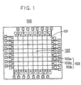
- Fig. 1 is a schematic plan view showing the chip structure of an IC device according to the embodiment of the invention
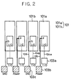
- Fig. 2 is a conceptual diagram for explaining a basic design of respective electrodes according to this embodiment.
- a chip 100 includes a circuit portion (active area) 102 in which a plurality of individual circuit portion (unit cell) 101 are arranged in the form of a matrix, and a plurality of electrodes 103 which are arranged in a zigzag fashion along the periphery of the active area 102 so as to surround it.
- an electrode group 103 consists of signal I/O electrodes 103a, power supply electrodes 103b, and ground electrodes 103c, the first electrodes 103a being disposed along the periphery a little to the center of the chip (referred to as 'inner periphery' hereinafter), and other two 103b, 103c being alternately disposed along the periphery outside the above inner periphery of the chip (referred to as 'outer periphery' hereinafter), so that each electrode can be connected with each unit cell 101 on the basis of one-to-one correspondence.
- the constitution of the IC device according to this embodiment will be more concretely described with reference to Fig. 2 .
- I/O signal input/output
- P power supply terminal
- the signal I/O terminal is connected in the same manner as the unit cell 101a, through a signal I/O wiring 104b, with the signal I/0 electrode 103a which is disposed along the inner periphery of the chip, and the ground terminal (G) is connected, through a ground wiring 106, with the ground electrode 103c which is disposed along the outer periphery of the chip.
- the unit cell 101a which is connected with the signal I/O electrode 103a and the power supply electrode 103b is alternately disposed with the unit cell 101b which is connected with the signal I/O electrode 103a and the ground electrode 103c. Accordingly, in the basic chip design according to this embodiment, two unit cells 101a and 101b are constituted as one set. Therefore, the basic design of one chip is completed by means of making copies of the above basic set by the necessary number and disposing them in a desired pattern.
- the signal I/O electrode 103a is located along the inner periphery of the chip, and the power supply electrode 103b and the ground electrode 103c are located along the outer periphery of the chip.
- the invention should not be limited to this way of electrode arrangement.
- the reverse electrode arrangement namely locating the power supply electrode 103b and the ground electrode 103c along the inner periphery of the chip, and locating the signal I/O electrode 103a along the outer periphery of the chip, may give the same effect as the former electrode arrangement.
- every unit cell 101 (101a, 101b) is connected with the signal I/O electrode 103a through respective signal I/O wirings 104a and 104b.
- the power supply terminal (P) and the ground terminal (G) of the unit cell 101 (101a, 101b) are alternately connected with the power supply and ground electrodes 103b and 103c through the power supply wiring 105 and the ground wiring 106, respectively.
- each of power supply and ground electrodes 103b, 103c come to be available separately from 208 signal I/O electrodes 103a corresponding to those unit cells.
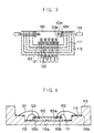
- Fig. 3 is a schematic plan view of a wiring portion while Fig. 4 is a schematic cross sectional view of the wiring portion as shown in Fig. 3 .
- the chip 100 which is required to execute the signal I/O operation at an operating frequency of about 80 MHz or more, it is very much effective countermeasure against noise to dispose the power supply and the ground separately from each other within the package.
- Epoxy board and ceramic board are used as a material for forming the multi-layer package body 110.
- the multi-layer package body 110 consists of the first layer 110a and the second layer 110b.
- the former (110a) includes a chip 100 disposed about in the center thereof, a common power supply ring 111 disposed so as to surround the chip 100, and a common ground ring 112 disposed so as to surround the ring 111, while the latter (110b) includes a signal I/O inner lead 113 disposed at a level higher than the first layer 110a.
- the signal I/O electrode 103a disposed along the inner periphery of the chip 100 is connected, through a wiring 121, with the inner lead 113 formed on the outer periphery of the package body 110.
- the power supply electrode 103b disposed along the outer periphery of the chip 100 is connected with the common power supply ring 111 positioned in the most inside of the package bogy 110 through a wiring 122.
- the ground electrode 103c also disposed along the outer periphery of the chip is connected with the common ground ring 112 positioned in the outside of the common power supply ring 111 through a wiring 123. The wire bonding process is completed when the above wiring operation is over.
- the signal I/O electrode 103a located along the inner periphery of the chip 100 is connected with the inner lead 113 of the package body 110 through the wiring 121, it becomes possible to keep the height of the wiring 121 higher. Therefore, different from the case of the prior art IC device ( Fig. 13 ), there is no fear that the height of the wiring 47c is made so lower that it gets in touch with the edge of the chip 41. Consequently, control of the wire bonding process is made easier.
- the power supply electrode 103b and the ground electrode 103c are provided separately from the signal I/O electrode 103a, the sufficient number of power supply and ground electrodes can be secured even in the case that all of available signal I/O electrodes 103a are fully used for maximum operation of the circuit portion 102. This makes it possible to select an optimum chip size corresponding to the necessary number of the electrodes. Furthermore, it becomes possible to reduce the chip size comparing to the case of prior art IC device, and to lower the manufacturing cost.
- each of power supply and ground electrodes 103b, 103c can be secured separately from 208 signal I/O electrodes 103a corresponding to those unit cells.
- the IC device according to the embodiment of the invention can comply with the demand for high speed operation at an operating frequency of 80 MHz or more. What is more advantageous, the optimum chip size to be used in the IC device operable at such a high operating frequency can be selected so as to correspond to the number of electrodes, thus enabling the manufacturing cost to be lowered.
- the chip can be selected so as to accommodate the designed optimum number of electrodes, and these electrodes can be disposed in a zigzag fashion, thus enabling the chip size to be comparatively made smaller to the number of electrodes.
- the height of wirings 122 and 123 can be kept higher to some extent. Consequently, there is no fear that wirings 122 and 123 get in touch with the edge of the chip 100, so that stable and high quality wirings can be achieved even through the ordinary wire bonding process without carrying out any special control therein.
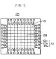
- Constitution of the IC device 200 according to this first example not forming part at the claimed invention is approximately similar to that of the IC device according to the embodiment of the invention, and a plurality of electrodes 203 are disposed in a zigzag fashion around the periphery of a circuit portion (active area) 202 in which a plurality of individual circuit portions (unit cells) 201 are arranged in the form of a matrix.
- Each electrode 203 is formed as an electrode group consisting of a signal I/O electrode 203a which is disposed along the inner periphery of the chip, and the power supply and ground electrodes 203b and 203c which are alternately disposed along the outer periphery of the chip and thus each electrode 203 is connected with each corresponding unit cells 201.
- the signal input/output (I/O) terminal of each unit cell 201 is connected, through a signal I/O wiring 204, with the signal I/O electrode 203a which is disposed along the inner periphery of the chip.
- the power supply terminal (P) of each unit cell 201 is connected, through a power supply wiring 205, with the power supply electrode 203b which is disposed along the outer periphery of the chip.
- the power supply wiring 205 for each unit cell 201 is further connected with a common wiring 205a.
- each unit cell 201 is connected, through a ground wiring 206, with the ground electrode 203c which is disposed along the outer periphery of the chip.
- the ground wiring 206 is also connected with another common wiring 206a in the same manner as the power supply wiring 205.
- each unit cell 201 is allowed to have an identical structure which is equally provided with the signal I/O terminal (I/O), the ground terminal (G), and the power supply terminal (P).
- the signal I/O electrode 203a is located along the inner periphery of the chip, and the power supply electrode 203b and the ground electrode 203c are located along the outer periphery of the chip.
- the first example should not be limited to this way of electrode arrangement.
- the reverse electrode arrangement namely locating the signal I/O electrode 203a along the outer periphery of the chip, and locating the power supply and ground electrodes 203b, 203c along the inner periphery of the chip, may give the same effect as the former electrode arrangement.
- the chip 200 is then manufactured through a predetermined wafer process using wafer masks prepared based on the above basic design. More concretely, the signal I/O electrode 203a is connected with the corresponding unit cell 201 through the signal I/O wiring 204.
- the power supply electrode 203b is connected with the power supply terminal (P) of the corresponding unit cell 201 through the power supply wiring 205 and the common wiring 205a.
- the ground electrode 203c is connected with the ground terminal (G) of the corresponding unit cell 201 through the ground wiring 206 and the common wiring 206a.
- each of power supply and ground electrodes 203b and 203c come to become available separately from 208 signal I/0 electrodes 203a corresponding to those unit cells.
- the structure of the unit cell 201 is unified, that the chip design is simplified, and also that the degree of freedom is expanded in the chip design.
- This IC device 300 has an almost identical constitution to those which have been described in connection with the embodiment of the invention and the first example not forming part of the claimed invention.
- electrodes 303a, 303b, and 303c are arranged in a zigzag fashion along the periphery of the unit cell 301a and 301b which are disposed in the form a matrix.
- a signal I/0 electrode 303a is disposed along the inner periphery of the chip 300 while the power supply electrode 303b and the ground electrode 303c are alternately disposed along the outer periphery of the chip 300.
- each of terminals provided in respective unit cells 301a and 301b is connected with necessary corresponding electrodes in the same manner as in the embodiment of the invention and the first example not forming part of the claimed invention, that is, the signal I/0 terminal (I/0) being connected with the signal I/0 electrode 303a through a signal I/0 wiring 304, the power supply terminal (P) with the power supply electrode 303b through a power supply wiring 305, and the ground terminal (G) with the ground electrode 303c through a ground wiring 306.
- a signal I/O terminal (I/O), power supply terminal (P) and ground terminal (G) for each corresponding unit cells 301a are provided as same as the first example not forming part of the claimed invention, in this example, adjacent unit cells 301a and 301b are designed to have such a mirror structure that two power supply terminals are disposed adjacent to each other and also two ground terminals are done the same.
- unit cells 301a and 301b are formed to have the mirror structure. Therefore, there is no need for them to be designed separately. That is, if the unit cell 301a is designed as a standard unit cell, the counterpart unit cell 301b can be obtained by just inverting the unit cell 301a in the mirror symmetry. Accordingly, two sorts of unit cells can be obtained by designing only one standard unit cell without carrying out two sorts of designs.
- the invention since power supply and ground electrodes can exist separately from the signal I/O electrode, the sufficient number of power supply and ground electrodes can be secured even in the case that all of available signal I/O electrodes are fully used for maximum operation of the circuit portion. This makes it possible to select an optimum chip size corresponding to the necessary number of the electrodes. Thus, it becomes possible to reduce the chip size comparing to the case of prior art IC device, and to lower the manufacturing cost.
- the invention may be preferably applied to the chip, especially one which is required to operate at a high operating frequency.
Landscapes
- Semiconductor Integrated Circuits (AREA)
- Design And Manufacture Of Integrated Circuits (AREA)
- Wire Bonding (AREA)
Claims (4)
- Halbleiter-IC-Gerät (100), umfassend:eine aktive Fläche (102), bestehend aus einer Mehrzahl von Elementzellen (101);eine Mehrzahl von Elektroden (103), die in einer Zickzack-Anordnung in einer ersten und einer zweiten Reihe entlang der Peripherie des aktiven Feldes (102) angeordnet sind;eine Mehrzahl von Signal-I/0-Elektroden (103a), die in der ersten Reihe der Zickzack-Elektrodenanordnung angeordnet sind;eine Mehrzahl von Energieversorgungselektroden (1 03b) und Masseelektroden (103c), die abwechselnd in der zweiten Reihe der Zickzack-Elektrodenanordnung angeordnet sind,dadurch gekennzeichnet, dassdie Mehrzahl von Elementzellen (101) erste Elementzellen (101 a), von denen jede einen Signal-I/O-Anschluss und einen Energieversorgungsanschluss aufweist, und zweite Elementzellen (101b) enthält, von denen jede einen Signal-I/O-Anschluss und einen Masseanschluss aufweist; unddas aktive Feld (102) durch abwechselndes Anordnen der ersten Elementzellen (101 a) und der zweiten Elementzellen (101b) erhalten wird.
- Halbleiter-IC-Gerät nach Anspruch 1, wobei sich eine Signal-I/O-Verdrahtung (104a, 104b) zum Verbinden des Signal-I/O-Anschlusses mit der Signal-I/O-Elektrode (103a) zwischen einer Energieversorgungsverdrahtung (105) zum Verbinden des Energieversorgungsanschlusses mit der Energieversorgungselektrode (103b) und einer Masseverdrahtung (106) zum Verbinden des Masseanschlusses mit der Masseelektrode (1 03c) befindet.
- Halbleiter-IC-Gerät nach Anspruch 1 oder 2, wobei sich die erste Reihe, auf welcher die Signal-I/O-Elektroden (103a) angeordnet sind, näher an dem aktiven Feld (102) als die zweite Reihe befindet, auf welcher die Energieversorgungselektroden (103b) und die Masseelektroden (103c) abwechselnd angeordnet sind.
- Baugruppe, umfassend ein Halbleiter-IC-Gerät in Übereinstimmung mit einem der vorhergehenden Ansprüche und einem Baugruppenkörper (110);
wobei der Baugruppenkörper (110) eine Mehrschicht-Struktur mit wenigstens zwei Schichten aufweist, wobei ein gemeinsamer Energieversorgungsring (111) und ein gemeinsamer Massering (112) auf einer ersten Schicht derart angeordnet sind, das Halbleiter-IC-Gerät (100) zu umgeben, und wobei ein Signal-I/O-Leiter (113) auf einer zweiten Schicht angeordnet ist.
Applications Claiming Priority (3)
| Application Number | Priority Date | Filing Date | Title |
|---|---|---|---|
| JP267788/97 | 1997-09-12 | ||
| JP26778897 | 1997-09-12 | ||
| JP26778897A JP3472455B2 (ja) | 1997-09-12 | 1997-09-12 | 半導体集積回路装置及びそのパッケージ構造 |
Publications (3)
| Publication Number | Publication Date |
|---|---|
| EP0902471A2 EP0902471A2 (de) | 1999-03-17 |
| EP0902471A3 EP0902471A3 (de) | 1999-11-03 |
| EP0902471B1 true EP0902471B1 (de) | 2009-12-30 |
Family
ID=17449607
Family Applications (1)
| Application Number | Title | Priority Date | Filing Date |
|---|---|---|---|
| EP98306868A Expired - Lifetime EP0902471B1 (de) | 1997-09-12 | 1998-08-27 | Integrierte Halbleiterschaltungsanordnung und Packungstruktur dafür |
Country Status (5)
| Country | Link |
|---|---|
| US (1) | US20010011768A1 (de) |
| EP (1) | EP0902471B1 (de) |
| JP (1) | JP3472455B2 (de) |
| KR (1) | KR100336082B1 (de) |
| DE (1) | DE69841416D1 (de) |
Families Citing this family (26)
| Publication number | Priority date | Publication date | Assignee | Title |
|---|---|---|---|---|
| US5360290A (en) * | 1991-12-13 | 1994-11-01 | Hitachi, Ltd. | Underground drainage facility, vertical-shaft multi-stage adjustable vane pump, and method of running drainage pump |
| TW473882B (en) * | 1998-07-06 | 2002-01-21 | Hitachi Ltd | Semiconductor device |
| US7525813B2 (en) * | 1998-07-06 | 2009-04-28 | Renesas Technology Corp. | Semiconductor device |
| US6833620B1 (en) * | 2000-11-28 | 2004-12-21 | Ati Technologies, Inc. | Apparatus having reduced input output area and method thereof |
| JP3715229B2 (ja) * | 2001-10-29 | 2005-11-09 | 沖電気工業株式会社 | 半導体装置及びその製造方法 |
| JP3741274B2 (ja) * | 2002-02-14 | 2006-02-01 | ローム株式会社 | 半導体装置 |
| US6836026B1 (en) * | 2003-01-14 | 2004-12-28 | Lsi Logic Corporation | Integrated circuit design for both input output limited and core limited integrated circuits |
| DE60336993D1 (de) | 2003-06-10 | 2011-06-16 | St Microelectronics Srl | Elektronische Halbleitervorrichtung und Verfahren zu deren Herstellung |
| JP4397210B2 (ja) * | 2003-10-20 | 2010-01-13 | ローム株式会社 | 半導体装置 |
| JP2005136246A (ja) * | 2003-10-31 | 2005-05-26 | Renesas Technology Corp | 半導体集積回路装置の製造方法 |
| JP4570868B2 (ja) * | 2003-12-26 | 2010-10-27 | ルネサスエレクトロニクス株式会社 | 半導体装置 |
| JP4533173B2 (ja) | 2004-02-24 | 2010-09-01 | キヤノン株式会社 | 半導体集積回路装置 |
| US7071561B2 (en) | 2004-06-08 | 2006-07-04 | Taiwan Semiconductor Manufacturing Company, Ltd. | Semiconductor device and method of manufacture thereof with two or more bond pad connections for each input/output cell |
| US7075179B1 (en) * | 2004-12-17 | 2006-07-11 | Lsi Logic Corporation | System for implementing a configurable integrated circuit |
| JP2006202866A (ja) | 2005-01-19 | 2006-08-03 | Nec Electronics Corp | 半導体装置 |
| WO2007015435A1 (ja) * | 2005-08-01 | 2007-02-08 | Matsushita Electric Industrial Co., Ltd. | 半導体装置 |
| US20070145607A1 (en) * | 2005-12-28 | 2007-06-28 | Mathew Ranjan J | System to wirebond power signals to flip-chip core |
| US7863737B2 (en) * | 2006-04-01 | 2011-01-04 | Stats Chippac Ltd. | Integrated circuit package system with wire bond pattern |
| JP2007335486A (ja) * | 2006-06-13 | 2007-12-27 | Sharp Corp | 半導体集積回路 |
| US7501709B1 (en) * | 2006-08-25 | 2009-03-10 | Altera Corporation | BGA package with wiring schemes having reduced current loop paths to improve cross talk control and characteristic impedance |
| JP2008091722A (ja) * | 2006-10-03 | 2008-04-17 | Matsushita Electric Ind Co Ltd | 半導体集積回路 |
| JP2009164195A (ja) | 2007-12-28 | 2009-07-23 | Panasonic Corp | 半導体チップ |
| JP2009200308A (ja) * | 2008-02-22 | 2009-09-03 | Oki Semiconductor Co Ltd | 半導体パッケージ |
| US8549257B2 (en) | 2011-01-10 | 2013-10-01 | Arm Limited | Area efficient arrangement of interface devices within an integrated circuit |
| JP6579111B2 (ja) | 2014-10-24 | 2019-09-25 | 株式会社ソシオネクスト | 半導体集積回路装置 |
| JP7208543B2 (ja) * | 2018-10-19 | 2023-01-19 | 株式会社ソシオネクスト | 半導体チップ |
Citations (1)
| Publication number | Priority date | Publication date | Assignee | Title |
|---|---|---|---|---|
| JPH0964232A (ja) * | 1995-08-23 | 1997-03-07 | Sumitomo Kinzoku Electro Device:Kk | セラミックパッケージ |
Family Cites Families (5)
| Publication number | Priority date | Publication date | Assignee | Title |
|---|---|---|---|---|
| JPS6393125A (ja) * | 1986-10-07 | 1988-04-23 | Nec Corp | 半導体集積回路 |
| JPH06105709B2 (ja) * | 1989-12-02 | 1994-12-21 | 東芝マイクロエレクトロニクス株式会社 | 半導体集積回路装置 |
| JPH04221837A (ja) * | 1990-12-21 | 1992-08-12 | Mitsubishi Electric Corp | 半導体装置 |
| US5155065A (en) * | 1992-03-16 | 1992-10-13 | Motorola, Inc. | Universal pad pitch layout |
| WO1995028005A2 (en) * | 1994-04-07 | 1995-10-19 | Vlsi Technology, Inc. | Staggered pad array |
-
1997
- 1997-09-12 JP JP26778897A patent/JP3472455B2/ja not_active Expired - Fee Related
-
1998
- 1998-08-20 US US09/137,153 patent/US20010011768A1/en not_active Abandoned
- 1998-08-27 DE DE69841416T patent/DE69841416D1/de not_active Expired - Lifetime
- 1998-08-27 EP EP98306868A patent/EP0902471B1/de not_active Expired - Lifetime
- 1998-09-08 KR KR1019980037041A patent/KR100336082B1/ko not_active Expired - Fee Related
Patent Citations (1)
| Publication number | Priority date | Publication date | Assignee | Title |
|---|---|---|---|---|
| JPH0964232A (ja) * | 1995-08-23 | 1997-03-07 | Sumitomo Kinzoku Electro Device:Kk | セラミックパッケージ |
Also Published As
| Publication number | Publication date |
|---|---|
| DE69841416D1 (de) | 2010-02-11 |
| JP3472455B2 (ja) | 2003-12-02 |
| KR19990029637A (ko) | 1999-04-26 |
| JPH1187399A (ja) | 1999-03-30 |
| EP0902471A3 (de) | 1999-11-03 |
| US20010011768A1 (en) | 2001-08-09 |
| EP0902471A2 (de) | 1999-03-17 |
| KR100336082B1 (ko) | 2002-06-20 |
Similar Documents
| Publication | Publication Date | Title |
|---|---|---|
| EP0902471B1 (de) | Integrierte Halbleiterschaltungsanordnung und Packungstruktur dafür | |
| JP3649993B2 (ja) | 半導体装置及び半導体装置の製造方法 | |
| US4972253A (en) | Programmable ceramic high performance custom package | |
| US8129837B2 (en) | Flip chip interconnection pad layout | |
| JP4592122B2 (ja) | パッケージ層の数を削減したフリップチップ・パッケージ | |
| US8680691B2 (en) | Semiconductor device having semiconductor member and mounting member | |
| US6762507B2 (en) | Internal circuit structure of semiconductor chip with array-type bonding pads and method of fabricating the same | |
| US5491364A (en) | Reduced stress terminal pattern for integrated circuit devices and packages | |
| US6677219B2 (en) | Method of forming a ball grid array package | |
| US5641978A (en) | Input/output buffer layout having overlapping buffers for reducing die area of pad-limited integrated circuit | |
| US5451814A (en) | Multi-chip module integrated circuit | |
| US5650660A (en) | Circuit pattern for a ball grid array integrated circuit package | |
| US6144091A (en) | Semiconductor device | |
| EP0957519B1 (de) | Kompatibles IC-Gehäuse und Methode zur Entwicklungsanpassungssicherung | |
| KR100336081B1 (ko) | 반도체 칩 | |
| EP0331206A2 (de) | Integrierte Schaltungshalbleiteranordnung mit Mehrschicht-Verbindungsstruktur | |
| KR20000062884A (ko) | 반도체 집적 회로 장치와 그 배선 배치 방법 | |
| US6828682B1 (en) | Substrate voltage connection | |
| JP2009004528A (ja) | 半導体装置 | |
| JPS59145542A (ja) | 大規模集積回路 | |
| JP3574004B2 (ja) | 半導体装置 | |
| JPS6248042A (ja) | マスタ−スライス方式半導体集積回路 | |
| KR20030041071A (ko) | 정렬 패드로서 본딩 패드를 사용하는 반도체 집적 회로 장치 | |
| JPS5966154A (ja) | 半導体装置 |
Legal Events
| Date | Code | Title | Description |
|---|---|---|---|
| PUAI | Public reference made under article 153(3) epc to a published international application that has entered the european phase |
Free format text: ORIGINAL CODE: 0009012 |
|
| AK | Designated contracting states |
Kind code of ref document: A2 Designated state(s): DE FR GB NL |
|
| AX | Request for extension of the european patent |
Free format text: AL;LT;LV;MK;RO;SI |
|
| PUAL | Search report despatched |
Free format text: ORIGINAL CODE: 0009013 |
|
| AK | Designated contracting states |
Kind code of ref document: A3 Designated state(s): AT BE CH CY DE DK ES FI FR GB GR IE IT LI LU MC NL PT SE |
|
| AX | Request for extension of the european patent |
Free format text: AL;LT;LV;MK;RO;SI |
|
| AKX | Designation fees paid | ||
| REG | Reference to a national code |
Ref country code: DE Ref legal event code: 8566 |
|
| 17P | Request for examination filed |
Effective date: 20000331 |
|
| RBV | Designated contracting states (corrected) |
Designated state(s): AT BE CH CY LI |
|
| RBV | Designated contracting states (corrected) |
Designated state(s): DE FR GB NL |
|
| RIC1 | Information provided on ipc code assigned before grant |
Ipc: H01L 23/528 20060101ALN20090507BHEP Ipc: H01L 23/13 20060101ALI20090507BHEP Ipc: H01L 23/485 20060101AFI20090507BHEP |
|
| GRAP | Despatch of communication of intention to grant a patent |
Free format text: ORIGINAL CODE: EPIDOSNIGR1 |
|
| GRAS | Grant fee paid |
Free format text: ORIGINAL CODE: EPIDOSNIGR3 |
|
| GRAA | (expected) grant |
Free format text: ORIGINAL CODE: 0009210 |
|
| AK | Designated contracting states |
Kind code of ref document: B1 Designated state(s): DE FR GB NL |
|
| REG | Reference to a national code |
Ref country code: GB Ref legal event code: FG4D |
|
| REF | Corresponds to: |
Ref document number: 69841416 Country of ref document: DE Date of ref document: 20100211 Kind code of ref document: P |
|
| REG | Reference to a national code |
Ref country code: NL Ref legal event code: VDEP Effective date: 20091230 |
|
| PG25 | Lapsed in a contracting state [announced via postgrant information from national office to epo] |
Ref country code: NL Free format text: LAPSE BECAUSE OF FAILURE TO SUBMIT A TRANSLATION OF THE DESCRIPTION OR TO PAY THE FEE WITHIN THE PRESCRIBED TIME-LIMIT Effective date: 20091230 |
|
| PLBE | No opposition filed within time limit |
Free format text: ORIGINAL CODE: 0009261 |
|
| STAA | Information on the status of an ep patent application or granted ep patent |
Free format text: STATUS: NO OPPOSITION FILED WITHIN TIME LIMIT |
|
| PGFP | Annual fee paid to national office [announced via postgrant information from national office to epo] |
Ref country code: FR Payment date: 20100903 Year of fee payment: 13 |
|
| 26N | No opposition filed |
Effective date: 20101001 |
|
| PGFP | Annual fee paid to national office [announced via postgrant information from national office to epo] |
Ref country code: GB Payment date: 20100813 Year of fee payment: 13 |
|
| PGFP | Annual fee paid to national office [announced via postgrant information from national office to epo] |
Ref country code: DE Payment date: 20101028 Year of fee payment: 13 |
|
| GBPC | Gb: european patent ceased through non-payment of renewal fee |
Effective date: 20110827 |
|
| REG | Reference to a national code |
Ref country code: FR Ref legal event code: ST Effective date: 20120430 |
|
| REG | Reference to a national code |
Ref country code: DE Ref legal event code: R119 Ref document number: 69841416 Country of ref document: DE Effective date: 20120301 |
|
| PG25 | Lapsed in a contracting state [announced via postgrant information from national office to epo] |
Ref country code: GB Free format text: LAPSE BECAUSE OF NON-PAYMENT OF DUE FEES Effective date: 20110827 Ref country code: FR Free format text: LAPSE BECAUSE OF NON-PAYMENT OF DUE FEES Effective date: 20110831 |
|
| PG25 | Lapsed in a contracting state [announced via postgrant information from national office to epo] |
Ref country code: DE Free format text: LAPSE BECAUSE OF NON-PAYMENT OF DUE FEES Effective date: 20120301 |