JP4570868B2 - 半導体装置 - Google Patents
半導体装置 Download PDFInfo
- Publication number
- JP4570868B2 JP4570868B2 JP2003433851A JP2003433851A JP4570868B2 JP 4570868 B2 JP4570868 B2 JP 4570868B2 JP 2003433851 A JP2003433851 A JP 2003433851A JP 2003433851 A JP2003433851 A JP 2003433851A JP 4570868 B2 JP4570868 B2 JP 4570868B2
- Authority
- JP
- Japan
- Prior art keywords
- bonding
- electrodes
- power supply
- semiconductor device
- electrode
- Prior art date
- Legal status (The legal status is an assumption and is not a legal conclusion. Google has not performed a legal analysis and makes no representation as to the accuracy of the status listed.)
- Expired - Fee Related
Links
- 239000004065 semiconductor Substances 0.000 title claims description 97
- 229910000679 solder Inorganic materials 0.000 claims description 8
- 230000015556 catabolic process Effects 0.000 claims description 7
- 239000000758 substrate Substances 0.000 description 11
- 239000010410 layer Substances 0.000 description 8
- 238000000034 method Methods 0.000 description 7
- 238000004519 manufacturing process Methods 0.000 description 5
- 230000000694 effects Effects 0.000 description 4
- 239000011229 interlayer Substances 0.000 description 3
- 239000010931 gold Substances 0.000 description 2
- 238000000059 patterning Methods 0.000 description 2
- 230000002093 peripheral effect Effects 0.000 description 2
- 238000007789 sealing Methods 0.000 description 2
- 208000033978 Device electrical impedance issue Diseases 0.000 description 1
- 239000004593 Epoxy Substances 0.000 description 1
- 229910052782 aluminium Inorganic materials 0.000 description 1
- XAGFODPZIPBFFR-UHFFFAOYSA-N aluminium Chemical compound [Al] XAGFODPZIPBFFR-UHFFFAOYSA-N 0.000 description 1
- 238000005516 engineering process Methods 0.000 description 1
- 230000005669 field effect Effects 0.000 description 1
- 238000007306 functionalization reaction Methods 0.000 description 1
- 239000003365 glass fiber Substances 0.000 description 1
- PCHJSUWPFVWCPO-UHFFFAOYSA-N gold Chemical compound [Au] PCHJSUWPFVWCPO-UHFFFAOYSA-N 0.000 description 1
- 229910052737 gold Inorganic materials 0.000 description 1
- 239000012212 insulator Substances 0.000 description 1
- 239000000463 material Substances 0.000 description 1
- 229910052751 metal Inorganic materials 0.000 description 1
- 239000002184 metal Substances 0.000 description 1
- 238000012986 modification Methods 0.000 description 1
- 230000004048 modification Effects 0.000 description 1
- 230000002265 prevention Effects 0.000 description 1
- 230000003252 repetitive effect Effects 0.000 description 1
- 229910052710 silicon Inorganic materials 0.000 description 1
- 239000010703 silicon Substances 0.000 description 1
- 238000005549 size reduction Methods 0.000 description 1
Images
Classifications
-
- H—ELECTRICITY
- H01—ELECTRIC ELEMENTS
- H01L—SEMICONDUCTOR DEVICES NOT COVERED BY CLASS H10
- H01L27/00—Devices consisting of a plurality of semiconductor or other solid-state components formed in or on a common substrate
- H01L27/02—Devices consisting of a plurality of semiconductor or other solid-state components formed in or on a common substrate including semiconductor components specially adapted for rectifying, oscillating, amplifying or switching and having at least one potential-jump barrier or surface barrier; including integrated passive circuit elements with at least one potential-jump barrier or surface barrier
- H01L27/04—Devices consisting of a plurality of semiconductor or other solid-state components formed in or on a common substrate including semiconductor components specially adapted for rectifying, oscillating, amplifying or switching and having at least one potential-jump barrier or surface barrier; including integrated passive circuit elements with at least one potential-jump barrier or surface barrier the substrate being a semiconductor body
- H01L27/10—Devices consisting of a plurality of semiconductor or other solid-state components formed in or on a common substrate including semiconductor components specially adapted for rectifying, oscillating, amplifying or switching and having at least one potential-jump barrier or surface barrier; including integrated passive circuit elements with at least one potential-jump barrier or surface barrier the substrate being a semiconductor body including a plurality of individual components in a repetitive configuration
- H01L27/118—Masterslice integrated circuits
- H01L27/11898—Input and output buffer/driver structures
-
- H—ELECTRICITY
- H01—ELECTRIC ELEMENTS
- H01L—SEMICONDUCTOR DEVICES NOT COVERED BY CLASS H10
- H01L21/00—Processes or apparatus adapted for the manufacture or treatment of semiconductor or solid state devices or of parts thereof
- H01L21/70—Manufacture or treatment of devices consisting of a plurality of solid state components formed in or on a common substrate or of parts thereof; Manufacture of integrated circuit devices or of parts thereof
- H01L21/77—Manufacture or treatment of devices consisting of a plurality of solid state components or integrated circuits formed in, or on, a common substrate
- H01L21/78—Manufacture or treatment of devices consisting of a plurality of solid state components or integrated circuits formed in, or on, a common substrate with subsequent division of the substrate into plural individual devices
- H01L21/82—Manufacture or treatment of devices consisting of a plurality of solid state components or integrated circuits formed in, or on, a common substrate with subsequent division of the substrate into plural individual devices to produce devices, e.g. integrated circuits, each consisting of a plurality of components
- H01L21/822—Manufacture or treatment of devices consisting of a plurality of solid state components or integrated circuits formed in, or on, a common substrate with subsequent division of the substrate into plural individual devices to produce devices, e.g. integrated circuits, each consisting of a plurality of components the substrate being a semiconductor, using silicon technology
- H01L21/8232—Field-effect technology
- H01L21/8234—MIS technology, i.e. integration processes of field effect transistors of the conductor-insulator-semiconductor type
- H01L21/8238—Complementary field-effect transistors, e.g. CMOS
- H01L21/823871—Complementary field-effect transistors, e.g. CMOS interconnection or wiring or contact manufacturing related aspects
-
- H—ELECTRICITY
- H01—ELECTRIC ELEMENTS
- H01L—SEMICONDUCTOR DEVICES NOT COVERED BY CLASS H10
- H01L23/00—Details of semiconductor or other solid state devices
- H01L23/48—Arrangements for conducting electric current to or from the solid state body in operation, e.g. leads, terminal arrangements ; Selection of materials therefor
- H01L23/488—Arrangements for conducting electric current to or from the solid state body in operation, e.g. leads, terminal arrangements ; Selection of materials therefor consisting of soldered or bonded constructions
- H01L23/498—Leads, i.e. metallisations or lead-frames on insulating substrates, e.g. chip carriers
- H01L23/49838—Geometry or layout
-
- H—ELECTRICITY
- H01—ELECTRIC ELEMENTS
- H01L—SEMICONDUCTOR DEVICES NOT COVERED BY CLASS H10
- H01L23/00—Details of semiconductor or other solid state devices
- H01L23/48—Arrangements for conducting electric current to or from the solid state body in operation, e.g. leads, terminal arrangements ; Selection of materials therefor
- H01L23/50—Arrangements for conducting electric current to or from the solid state body in operation, e.g. leads, terminal arrangements ; Selection of materials therefor for integrated circuit devices, e.g. power bus, number of leads
-
- H—ELECTRICITY
- H01—ELECTRIC ELEMENTS
- H01L—SEMICONDUCTOR DEVICES NOT COVERED BY CLASS H10
- H01L23/00—Details of semiconductor or other solid state devices
- H01L23/58—Structural electrical arrangements for semiconductor devices not otherwise provided for, e.g. in combination with batteries
- H01L23/64—Impedance arrangements
- H01L23/66—High-frequency adaptations
-
- H—ELECTRICITY
- H01—ELECTRIC ELEMENTS
- H01L—SEMICONDUCTOR DEVICES NOT COVERED BY CLASS H10
- H01L24/00—Arrangements for connecting or disconnecting semiconductor or solid-state bodies; Methods or apparatus related thereto
- H01L24/01—Means for bonding being attached to, or being formed on, the surface to be connected, e.g. chip-to-package, die-attach, "first-level" interconnects; Manufacturing methods related thereto
- H01L24/02—Bonding areas ; Manufacturing methods related thereto
- H01L24/04—Structure, shape, material or disposition of the bonding areas prior to the connecting process
- H01L24/05—Structure, shape, material or disposition of the bonding areas prior to the connecting process of an individual bonding area
-
- H—ELECTRICITY
- H01—ELECTRIC ELEMENTS
- H01L—SEMICONDUCTOR DEVICES NOT COVERED BY CLASS H10
- H01L24/00—Arrangements for connecting or disconnecting semiconductor or solid-state bodies; Methods or apparatus related thereto
- H01L24/01—Means for bonding being attached to, or being formed on, the surface to be connected, e.g. chip-to-package, die-attach, "first-level" interconnects; Manufacturing methods related thereto
- H01L24/02—Bonding areas ; Manufacturing methods related thereto
- H01L24/04—Structure, shape, material or disposition of the bonding areas prior to the connecting process
- H01L24/06—Structure, shape, material or disposition of the bonding areas prior to the connecting process of a plurality of bonding areas
-
- H—ELECTRICITY
- H01—ELECTRIC ELEMENTS
- H01L—SEMICONDUCTOR DEVICES NOT COVERED BY CLASS H10
- H01L24/00—Arrangements for connecting or disconnecting semiconductor or solid-state bodies; Methods or apparatus related thereto
- H01L24/01—Means for bonding being attached to, or being formed on, the surface to be connected, e.g. chip-to-package, die-attach, "first-level" interconnects; Manufacturing methods related thereto
- H01L24/42—Wire connectors; Manufacturing methods related thereto
- H01L24/47—Structure, shape, material or disposition of the wire connectors after the connecting process
- H01L24/48—Structure, shape, material or disposition of the wire connectors after the connecting process of an individual wire connector
-
- H—ELECTRICITY
- H01—ELECTRIC ELEMENTS
- H01L—SEMICONDUCTOR DEVICES NOT COVERED BY CLASS H10
- H01L24/00—Arrangements for connecting or disconnecting semiconductor or solid-state bodies; Methods or apparatus related thereto
- H01L24/01—Means for bonding being attached to, or being formed on, the surface to be connected, e.g. chip-to-package, die-attach, "first-level" interconnects; Manufacturing methods related thereto
- H01L24/42—Wire connectors; Manufacturing methods related thereto
- H01L24/47—Structure, shape, material or disposition of the wire connectors after the connecting process
- H01L24/49—Structure, shape, material or disposition of the wire connectors after the connecting process of a plurality of wire connectors
-
- H—ELECTRICITY
- H01—ELECTRIC ELEMENTS
- H01L—SEMICONDUCTOR DEVICES NOT COVERED BY CLASS H10
- H01L24/00—Arrangements for connecting or disconnecting semiconductor or solid-state bodies; Methods or apparatus related thereto
- H01L24/80—Methods for connecting semiconductor or other solid state bodies using means for bonding being attached to, or being formed on, the surface to be connected
- H01L24/85—Methods for connecting semiconductor or other solid state bodies using means for bonding being attached to, or being formed on, the surface to be connected using a wire connector
-
- H—ELECTRICITY
- H01—ELECTRIC ELEMENTS
- H01L—SEMICONDUCTOR DEVICES NOT COVERED BY CLASS H10
- H01L2223/00—Details relating to semiconductor or other solid state devices covered by the group H01L23/00
- H01L2223/58—Structural electrical arrangements for semiconductor devices not otherwise provided for
- H01L2223/64—Impedance arrangements
- H01L2223/66—High-frequency adaptations
- H01L2223/6605—High-frequency electrical connections
- H01L2223/6611—Wire connections
-
- H—ELECTRICITY
- H01—ELECTRIC ELEMENTS
- H01L—SEMICONDUCTOR DEVICES NOT COVERED BY CLASS H10
- H01L2224/00—Indexing scheme for arrangements for connecting or disconnecting semiconductor or solid-state bodies and methods related thereto as covered by H01L24/00
- H01L2224/01—Means for bonding being attached to, or being formed on, the surface to be connected, e.g. chip-to-package, die-attach, "first-level" interconnects; Manufacturing methods related thereto
- H01L2224/02—Bonding areas; Manufacturing methods related thereto
- H01L2224/023—Redistribution layers [RDL] for bonding areas
-
- H—ELECTRICITY
- H01—ELECTRIC ELEMENTS
- H01L—SEMICONDUCTOR DEVICES NOT COVERED BY CLASS H10
- H01L2224/00—Indexing scheme for arrangements for connecting or disconnecting semiconductor or solid-state bodies and methods related thereto as covered by H01L24/00
- H01L2224/01—Means for bonding being attached to, or being formed on, the surface to be connected, e.g. chip-to-package, die-attach, "first-level" interconnects; Manufacturing methods related thereto
- H01L2224/02—Bonding areas; Manufacturing methods related thereto
- H01L2224/04—Structure, shape, material or disposition of the bonding areas prior to the connecting process
- H01L2224/04042—Bonding areas specifically adapted for wire connectors, e.g. wirebond pads
-
- H—ELECTRICITY
- H01—ELECTRIC ELEMENTS
- H01L—SEMICONDUCTOR DEVICES NOT COVERED BY CLASS H10
- H01L2224/00—Indexing scheme for arrangements for connecting or disconnecting semiconductor or solid-state bodies and methods related thereto as covered by H01L24/00
- H01L2224/01—Means for bonding being attached to, or being formed on, the surface to be connected, e.g. chip-to-package, die-attach, "first-level" interconnects; Manufacturing methods related thereto
- H01L2224/02—Bonding areas; Manufacturing methods related thereto
- H01L2224/04—Structure, shape, material or disposition of the bonding areas prior to the connecting process
- H01L2224/05—Structure, shape, material or disposition of the bonding areas prior to the connecting process of an individual bonding area
- H01L2224/0554—External layer
- H01L2224/0555—Shape
- H01L2224/05552—Shape in top view
- H01L2224/05553—Shape in top view being rectangular
-
- H—ELECTRICITY
- H01—ELECTRIC ELEMENTS
- H01L—SEMICONDUCTOR DEVICES NOT COVERED BY CLASS H10
- H01L2224/00—Indexing scheme for arrangements for connecting or disconnecting semiconductor or solid-state bodies and methods related thereto as covered by H01L24/00
- H01L2224/01—Means for bonding being attached to, or being formed on, the surface to be connected, e.g. chip-to-package, die-attach, "first-level" interconnects; Manufacturing methods related thereto
- H01L2224/02—Bonding areas; Manufacturing methods related thereto
- H01L2224/04—Structure, shape, material or disposition of the bonding areas prior to the connecting process
- H01L2224/05—Structure, shape, material or disposition of the bonding areas prior to the connecting process of an individual bonding area
- H01L2224/0554—External layer
- H01L2224/0555—Shape
- H01L2224/05556—Shape in side view
-
- H—ELECTRICITY
- H01—ELECTRIC ELEMENTS
- H01L—SEMICONDUCTOR DEVICES NOT COVERED BY CLASS H10
- H01L2224/00—Indexing scheme for arrangements for connecting or disconnecting semiconductor or solid-state bodies and methods related thereto as covered by H01L24/00
- H01L2224/01—Means for bonding being attached to, or being formed on, the surface to be connected, e.g. chip-to-package, die-attach, "first-level" interconnects; Manufacturing methods related thereto
- H01L2224/02—Bonding areas; Manufacturing methods related thereto
- H01L2224/04—Structure, shape, material or disposition of the bonding areas prior to the connecting process
- H01L2224/05—Structure, shape, material or disposition of the bonding areas prior to the connecting process of an individual bonding area
- H01L2224/0554—External layer
- H01L2224/05599—Material
- H01L2224/056—Material with a principal constituent of the material being a metal or a metalloid, e.g. boron [B], silicon [Si], germanium [Ge], arsenic [As], antimony [Sb], tellurium [Te] and polonium [Po], and alloys thereof
- H01L2224/05617—Material with a principal constituent of the material being a metal or a metalloid, e.g. boron [B], silicon [Si], germanium [Ge], arsenic [As], antimony [Sb], tellurium [Te] and polonium [Po], and alloys thereof the principal constituent melting at a temperature of greater than or equal to 400°C and less than 950°C
- H01L2224/05624—Aluminium [Al] as principal constituent
-
- H—ELECTRICITY
- H01—ELECTRIC ELEMENTS
- H01L—SEMICONDUCTOR DEVICES NOT COVERED BY CLASS H10
- H01L2224/00—Indexing scheme for arrangements for connecting or disconnecting semiconductor or solid-state bodies and methods related thereto as covered by H01L24/00
- H01L2224/01—Means for bonding being attached to, or being formed on, the surface to be connected, e.g. chip-to-package, die-attach, "first-level" interconnects; Manufacturing methods related thereto
- H01L2224/02—Bonding areas; Manufacturing methods related thereto
- H01L2224/04—Structure, shape, material or disposition of the bonding areas prior to the connecting process
- H01L2224/06—Structure, shape, material or disposition of the bonding areas prior to the connecting process of a plurality of bonding areas
- H01L2224/061—Disposition
- H01L2224/0612—Layout
- H01L2224/0615—Mirror array, i.e. array having only a reflection symmetry, i.e. bilateral symmetry
- H01L2224/06153—Mirror array, i.e. array having only a reflection symmetry, i.e. bilateral symmetry with a staggered arrangement, e.g. depopulated array
-
- H—ELECTRICITY
- H01—ELECTRIC ELEMENTS
- H01L—SEMICONDUCTOR DEVICES NOT COVERED BY CLASS H10
- H01L2224/00—Indexing scheme for arrangements for connecting or disconnecting semiconductor or solid-state bodies and methods related thereto as covered by H01L24/00
- H01L2224/01—Means for bonding being attached to, or being formed on, the surface to be connected, e.g. chip-to-package, die-attach, "first-level" interconnects; Manufacturing methods related thereto
- H01L2224/42—Wire connectors; Manufacturing methods related thereto
- H01L2224/44—Structure, shape, material or disposition of the wire connectors prior to the connecting process
- H01L2224/45—Structure, shape, material or disposition of the wire connectors prior to the connecting process of an individual wire connector
- H01L2224/45001—Core members of the connector
- H01L2224/4501—Shape
- H01L2224/45012—Cross-sectional shape
- H01L2224/45015—Cross-sectional shape being circular
-
- H—ELECTRICITY
- H01—ELECTRIC ELEMENTS
- H01L—SEMICONDUCTOR DEVICES NOT COVERED BY CLASS H10
- H01L2224/00—Indexing scheme for arrangements for connecting or disconnecting semiconductor or solid-state bodies and methods related thereto as covered by H01L24/00
- H01L2224/01—Means for bonding being attached to, or being formed on, the surface to be connected, e.g. chip-to-package, die-attach, "first-level" interconnects; Manufacturing methods related thereto
- H01L2224/42—Wire connectors; Manufacturing methods related thereto
- H01L2224/44—Structure, shape, material or disposition of the wire connectors prior to the connecting process
- H01L2224/45—Structure, shape, material or disposition of the wire connectors prior to the connecting process of an individual wire connector
- H01L2224/45001—Core members of the connector
- H01L2224/45099—Material
- H01L2224/451—Material with a principal constituent of the material being a metal or a metalloid, e.g. boron (B), silicon (Si), germanium (Ge), arsenic (As), antimony (Sb), tellurium (Te) and polonium (Po), and alloys thereof
- H01L2224/45138—Material with a principal constituent of the material being a metal or a metalloid, e.g. boron (B), silicon (Si), germanium (Ge), arsenic (As), antimony (Sb), tellurium (Te) and polonium (Po), and alloys thereof the principal constituent melting at a temperature of greater than or equal to 950°C and less than 1550°C
- H01L2224/45144—Gold (Au) as principal constituent
-
- H—ELECTRICITY
- H01—ELECTRIC ELEMENTS
- H01L—SEMICONDUCTOR DEVICES NOT COVERED BY CLASS H10
- H01L2224/00—Indexing scheme for arrangements for connecting or disconnecting semiconductor or solid-state bodies and methods related thereto as covered by H01L24/00
- H01L2224/01—Means for bonding being attached to, or being formed on, the surface to be connected, e.g. chip-to-package, die-attach, "first-level" interconnects; Manufacturing methods related thereto
- H01L2224/42—Wire connectors; Manufacturing methods related thereto
- H01L2224/47—Structure, shape, material or disposition of the wire connectors after the connecting process
- H01L2224/48—Structure, shape, material or disposition of the wire connectors after the connecting process of an individual wire connector
- H01L2224/4805—Shape
- H01L2224/4809—Loop shape
- H01L2224/48091—Arched
-
- H—ELECTRICITY
- H01—ELECTRIC ELEMENTS
- H01L—SEMICONDUCTOR DEVICES NOT COVERED BY CLASS H10
- H01L2224/00—Indexing scheme for arrangements for connecting or disconnecting semiconductor or solid-state bodies and methods related thereto as covered by H01L24/00
- H01L2224/01—Means for bonding being attached to, or being formed on, the surface to be connected, e.g. chip-to-package, die-attach, "first-level" interconnects; Manufacturing methods related thereto
- H01L2224/42—Wire connectors; Manufacturing methods related thereto
- H01L2224/47—Structure, shape, material or disposition of the wire connectors after the connecting process
- H01L2224/48—Structure, shape, material or disposition of the wire connectors after the connecting process of an individual wire connector
- H01L2224/4805—Shape
- H01L2224/4809—Loop shape
- H01L2224/48095—Kinked
-
- H—ELECTRICITY
- H01—ELECTRIC ELEMENTS
- H01L—SEMICONDUCTOR DEVICES NOT COVERED BY CLASS H10
- H01L2224/00—Indexing scheme for arrangements for connecting or disconnecting semiconductor or solid-state bodies and methods related thereto as covered by H01L24/00
- H01L2224/01—Means for bonding being attached to, or being formed on, the surface to be connected, e.g. chip-to-package, die-attach, "first-level" interconnects; Manufacturing methods related thereto
- H01L2224/42—Wire connectors; Manufacturing methods related thereto
- H01L2224/47—Structure, shape, material or disposition of the wire connectors after the connecting process
- H01L2224/48—Structure, shape, material or disposition of the wire connectors after the connecting process of an individual wire connector
- H01L2224/481—Disposition
- H01L2224/48151—Connecting between a semiconductor or solid-state body and an item not being a semiconductor or solid-state body, e.g. chip-to-substrate, chip-to-passive
- H01L2224/48221—Connecting between a semiconductor or solid-state body and an item not being a semiconductor or solid-state body, e.g. chip-to-substrate, chip-to-passive the body and the item being stacked
- H01L2224/48225—Connecting between a semiconductor or solid-state body and an item not being a semiconductor or solid-state body, e.g. chip-to-substrate, chip-to-passive the body and the item being stacked the item being non-metallic, e.g. insulating substrate with or without metallisation
- H01L2224/48227—Connecting between a semiconductor or solid-state body and an item not being a semiconductor or solid-state body, e.g. chip-to-substrate, chip-to-passive the body and the item being stacked the item being non-metallic, e.g. insulating substrate with or without metallisation connecting the wire to a bond pad of the item
-
- H—ELECTRICITY
- H01—ELECTRIC ELEMENTS
- H01L—SEMICONDUCTOR DEVICES NOT COVERED BY CLASS H10
- H01L2224/00—Indexing scheme for arrangements for connecting or disconnecting semiconductor or solid-state bodies and methods related thereto as covered by H01L24/00
- H01L2224/01—Means for bonding being attached to, or being formed on, the surface to be connected, e.g. chip-to-package, die-attach, "first-level" interconnects; Manufacturing methods related thereto
- H01L2224/42—Wire connectors; Manufacturing methods related thereto
- H01L2224/47—Structure, shape, material or disposition of the wire connectors after the connecting process
- H01L2224/48—Structure, shape, material or disposition of the wire connectors after the connecting process of an individual wire connector
- H01L2224/481—Disposition
- H01L2224/48151—Connecting between a semiconductor or solid-state body and an item not being a semiconductor or solid-state body, e.g. chip-to-substrate, chip-to-passive
- H01L2224/48221—Connecting between a semiconductor or solid-state body and an item not being a semiconductor or solid-state body, e.g. chip-to-substrate, chip-to-passive the body and the item being stacked
- H01L2224/48225—Connecting between a semiconductor or solid-state body and an item not being a semiconductor or solid-state body, e.g. chip-to-substrate, chip-to-passive the body and the item being stacked the item being non-metallic, e.g. insulating substrate with or without metallisation
- H01L2224/48233—Connecting between a semiconductor or solid-state body and an item not being a semiconductor or solid-state body, e.g. chip-to-substrate, chip-to-passive the body and the item being stacked the item being non-metallic, e.g. insulating substrate with or without metallisation connecting the wire to a potential ring of the item
-
- H—ELECTRICITY
- H01—ELECTRIC ELEMENTS
- H01L—SEMICONDUCTOR DEVICES NOT COVERED BY CLASS H10
- H01L2224/00—Indexing scheme for arrangements for connecting or disconnecting semiconductor or solid-state bodies and methods related thereto as covered by H01L24/00
- H01L2224/01—Means for bonding being attached to, or being formed on, the surface to be connected, e.g. chip-to-package, die-attach, "first-level" interconnects; Manufacturing methods related thereto
- H01L2224/42—Wire connectors; Manufacturing methods related thereto
- H01L2224/47—Structure, shape, material or disposition of the wire connectors after the connecting process
- H01L2224/48—Structure, shape, material or disposition of the wire connectors after the connecting process of an individual wire connector
- H01L2224/481—Disposition
- H01L2224/48151—Connecting between a semiconductor or solid-state body and an item not being a semiconductor or solid-state body, e.g. chip-to-substrate, chip-to-passive
- H01L2224/48221—Connecting between a semiconductor or solid-state body and an item not being a semiconductor or solid-state body, e.g. chip-to-substrate, chip-to-passive the body and the item being stacked
- H01L2224/48225—Connecting between a semiconductor or solid-state body and an item not being a semiconductor or solid-state body, e.g. chip-to-substrate, chip-to-passive the body and the item being stacked the item being non-metallic, e.g. insulating substrate with or without metallisation
- H01L2224/48237—Connecting between a semiconductor or solid-state body and an item not being a semiconductor or solid-state body, e.g. chip-to-substrate, chip-to-passive the body and the item being stacked the item being non-metallic, e.g. insulating substrate with or without metallisation connecting the wire to a die pad of the item
-
- H—ELECTRICITY
- H01—ELECTRIC ELEMENTS
- H01L—SEMICONDUCTOR DEVICES NOT COVERED BY CLASS H10
- H01L2224/00—Indexing scheme for arrangements for connecting or disconnecting semiconductor or solid-state bodies and methods related thereto as covered by H01L24/00
- H01L2224/01—Means for bonding being attached to, or being formed on, the surface to be connected, e.g. chip-to-package, die-attach, "first-level" interconnects; Manufacturing methods related thereto
- H01L2224/42—Wire connectors; Manufacturing methods related thereto
- H01L2224/47—Structure, shape, material or disposition of the wire connectors after the connecting process
- H01L2224/48—Structure, shape, material or disposition of the wire connectors after the connecting process of an individual wire connector
- H01L2224/484—Connecting portions
- H01L2224/48463—Connecting portions the connecting portion on the bonding area of the semiconductor or solid-state body being a ball bond
- H01L2224/48465—Connecting portions the connecting portion on the bonding area of the semiconductor or solid-state body being a ball bond the other connecting portion not on the bonding area being a wedge bond, i.e. ball-to-wedge, regular stitch
-
- H—ELECTRICITY
- H01—ELECTRIC ELEMENTS
- H01L—SEMICONDUCTOR DEVICES NOT COVERED BY CLASS H10
- H01L2224/00—Indexing scheme for arrangements for connecting or disconnecting semiconductor or solid-state bodies and methods related thereto as covered by H01L24/00
- H01L2224/01—Means for bonding being attached to, or being formed on, the surface to be connected, e.g. chip-to-package, die-attach, "first-level" interconnects; Manufacturing methods related thereto
- H01L2224/42—Wire connectors; Manufacturing methods related thereto
- H01L2224/47—Structure, shape, material or disposition of the wire connectors after the connecting process
- H01L2224/48—Structure, shape, material or disposition of the wire connectors after the connecting process of an individual wire connector
- H01L2224/485—Material
- H01L2224/48505—Material at the bonding interface
- H01L2224/48599—Principal constituent of the connecting portion of the wire connector being Gold (Au)
- H01L2224/486—Principal constituent of the connecting portion of the wire connector being Gold (Au) with a principal constituent of the bonding area being a metal or a metalloid, e.g. boron (B), silicon (Si), germanium (Ge), arsenic (As), antimony (Sb), tellurium (Te) and polonium (Po), and alloys thereof
- H01L2224/48617—Principal constituent of the connecting portion of the wire connector being Gold (Au) with a principal constituent of the bonding area being a metal or a metalloid, e.g. boron (B), silicon (Si), germanium (Ge), arsenic (As), antimony (Sb), tellurium (Te) and polonium (Po), and alloys thereof the principal constituent melting at a temperature of greater than or equal to 400°C and less than 950 °C
- H01L2224/48624—Aluminium (Al) as principal constituent
-
- H—ELECTRICITY
- H01—ELECTRIC ELEMENTS
- H01L—SEMICONDUCTOR DEVICES NOT COVERED BY CLASS H10
- H01L2224/00—Indexing scheme for arrangements for connecting or disconnecting semiconductor or solid-state bodies and methods related thereto as covered by H01L24/00
- H01L2224/01—Means for bonding being attached to, or being formed on, the surface to be connected, e.g. chip-to-package, die-attach, "first-level" interconnects; Manufacturing methods related thereto
- H01L2224/42—Wire connectors; Manufacturing methods related thereto
- H01L2224/47—Structure, shape, material or disposition of the wire connectors after the connecting process
- H01L2224/49—Structure, shape, material or disposition of the wire connectors after the connecting process of a plurality of wire connectors
- H01L2224/4901—Structure
- H01L2224/4903—Connectors having different sizes, e.g. different diameters
-
- H—ELECTRICITY
- H01—ELECTRIC ELEMENTS
- H01L—SEMICONDUCTOR DEVICES NOT COVERED BY CLASS H10
- H01L2224/00—Indexing scheme for arrangements for connecting or disconnecting semiconductor or solid-state bodies and methods related thereto as covered by H01L24/00
- H01L2224/01—Means for bonding being attached to, or being formed on, the surface to be connected, e.g. chip-to-package, die-attach, "first-level" interconnects; Manufacturing methods related thereto
- H01L2224/42—Wire connectors; Manufacturing methods related thereto
- H01L2224/47—Structure, shape, material or disposition of the wire connectors after the connecting process
- H01L2224/49—Structure, shape, material or disposition of the wire connectors after the connecting process of a plurality of wire connectors
- H01L2224/4905—Shape
- H01L2224/49051—Connectors having different shapes
-
- H—ELECTRICITY
- H01—ELECTRIC ELEMENTS
- H01L—SEMICONDUCTOR DEVICES NOT COVERED BY CLASS H10
- H01L2224/00—Indexing scheme for arrangements for connecting or disconnecting semiconductor or solid-state bodies and methods related thereto as covered by H01L24/00
- H01L2224/01—Means for bonding being attached to, or being formed on, the surface to be connected, e.g. chip-to-package, die-attach, "first-level" interconnects; Manufacturing methods related thereto
- H01L2224/42—Wire connectors; Manufacturing methods related thereto
- H01L2224/47—Structure, shape, material or disposition of the wire connectors after the connecting process
- H01L2224/49—Structure, shape, material or disposition of the wire connectors after the connecting process of a plurality of wire connectors
- H01L2224/491—Disposition
- H01L2224/4912—Layout
- H01L2224/49171—Fan-out arrangements
-
- H—ELECTRICITY
- H01—ELECTRIC ELEMENTS
- H01L—SEMICONDUCTOR DEVICES NOT COVERED BY CLASS H10
- H01L2224/00—Indexing scheme for arrangements for connecting or disconnecting semiconductor or solid-state bodies and methods related thereto as covered by H01L24/00
- H01L2224/01—Means for bonding being attached to, or being formed on, the surface to be connected, e.g. chip-to-package, die-attach, "first-level" interconnects; Manufacturing methods related thereto
- H01L2224/42—Wire connectors; Manufacturing methods related thereto
- H01L2224/47—Structure, shape, material or disposition of the wire connectors after the connecting process
- H01L2224/49—Structure, shape, material or disposition of the wire connectors after the connecting process of a plurality of wire connectors
- H01L2224/494—Connecting portions
- H01L2224/4943—Connecting portions the connecting portions being staggered
- H01L2224/49431—Connecting portions the connecting portions being staggered on the semiconductor or solid-state body
-
- H—ELECTRICITY
- H01—ELECTRIC ELEMENTS
- H01L—SEMICONDUCTOR DEVICES NOT COVERED BY CLASS H10
- H01L2224/00—Indexing scheme for arrangements for connecting or disconnecting semiconductor or solid-state bodies and methods related thereto as covered by H01L24/00
- H01L2224/01—Means for bonding being attached to, or being formed on, the surface to be connected, e.g. chip-to-package, die-attach, "first-level" interconnects; Manufacturing methods related thereto
- H01L2224/42—Wire connectors; Manufacturing methods related thereto
- H01L2224/47—Structure, shape, material or disposition of the wire connectors after the connecting process
- H01L2224/49—Structure, shape, material or disposition of the wire connectors after the connecting process of a plurality of wire connectors
- H01L2224/494—Connecting portions
- H01L2224/4943—Connecting portions the connecting portions being staggered
- H01L2224/49433—Connecting portions the connecting portions being staggered outside the semiconductor or solid-state body
-
- H—ELECTRICITY
- H01—ELECTRIC ELEMENTS
- H01L—SEMICONDUCTOR DEVICES NOT COVERED BY CLASS H10
- H01L2224/00—Indexing scheme for arrangements for connecting or disconnecting semiconductor or solid-state bodies and methods related thereto as covered by H01L24/00
- H01L2224/80—Methods for connecting semiconductor or other solid state bodies using means for bonding being attached to, or being formed on, the surface to be connected
- H01L2224/85—Methods for connecting semiconductor or other solid state bodies using means for bonding being attached to, or being formed on, the surface to be connected using a wire connector
-
- H—ELECTRICITY
- H01—ELECTRIC ELEMENTS
- H01L—SEMICONDUCTOR DEVICES NOT COVERED BY CLASS H10
- H01L24/00—Arrangements for connecting or disconnecting semiconductor or solid-state bodies; Methods or apparatus related thereto
- H01L24/01—Means for bonding being attached to, or being formed on, the surface to be connected, e.g. chip-to-package, die-attach, "first-level" interconnects; Manufacturing methods related thereto
- H01L24/42—Wire connectors; Manufacturing methods related thereto
- H01L24/44—Structure, shape, material or disposition of the wire connectors prior to the connecting process
- H01L24/45—Structure, shape, material or disposition of the wire connectors prior to the connecting process of an individual wire connector
-
- H—ELECTRICITY
- H01—ELECTRIC ELEMENTS
- H01L—SEMICONDUCTOR DEVICES NOT COVERED BY CLASS H10
- H01L2924/00—Indexing scheme for arrangements or methods for connecting or disconnecting semiconductor or solid-state bodies as covered by H01L24/00
- H01L2924/0001—Technical content checked by a classifier
- H01L2924/00014—Technical content checked by a classifier the subject-matter covered by the group, the symbol of which is combined with the symbol of this group, being disclosed without further technical details
-
- H—ELECTRICITY
- H01—ELECTRIC ELEMENTS
- H01L—SEMICONDUCTOR DEVICES NOT COVERED BY CLASS H10
- H01L2924/00—Indexing scheme for arrangements or methods for connecting or disconnecting semiconductor or solid-state bodies as covered by H01L24/00
- H01L2924/01—Chemical elements
- H01L2924/01005—Boron [B]
-
- H—ELECTRICITY
- H01—ELECTRIC ELEMENTS
- H01L—SEMICONDUCTOR DEVICES NOT COVERED BY CLASS H10
- H01L2924/00—Indexing scheme for arrangements or methods for connecting or disconnecting semiconductor or solid-state bodies as covered by H01L24/00
- H01L2924/01—Chemical elements
- H01L2924/01006—Carbon [C]
-
- H—ELECTRICITY
- H01—ELECTRIC ELEMENTS
- H01L—SEMICONDUCTOR DEVICES NOT COVERED BY CLASS H10
- H01L2924/00—Indexing scheme for arrangements or methods for connecting or disconnecting semiconductor or solid-state bodies as covered by H01L24/00
- H01L2924/01—Chemical elements
- H01L2924/01013—Aluminum [Al]
-
- H—ELECTRICITY
- H01—ELECTRIC ELEMENTS
- H01L—SEMICONDUCTOR DEVICES NOT COVERED BY CLASS H10
- H01L2924/00—Indexing scheme for arrangements or methods for connecting or disconnecting semiconductor or solid-state bodies as covered by H01L24/00
- H01L2924/01—Chemical elements
- H01L2924/01014—Silicon [Si]
-
- H—ELECTRICITY
- H01—ELECTRIC ELEMENTS
- H01L—SEMICONDUCTOR DEVICES NOT COVERED BY CLASS H10
- H01L2924/00—Indexing scheme for arrangements or methods for connecting or disconnecting semiconductor or solid-state bodies as covered by H01L24/00
- H01L2924/01—Chemical elements
- H01L2924/01015—Phosphorus [P]
-
- H—ELECTRICITY
- H01—ELECTRIC ELEMENTS
- H01L—SEMICONDUCTOR DEVICES NOT COVERED BY CLASS H10
- H01L2924/00—Indexing scheme for arrangements or methods for connecting or disconnecting semiconductor or solid-state bodies as covered by H01L24/00
- H01L2924/01—Chemical elements
- H01L2924/01023—Vanadium [V]
-
- H—ELECTRICITY
- H01—ELECTRIC ELEMENTS
- H01L—SEMICONDUCTOR DEVICES NOT COVERED BY CLASS H10
- H01L2924/00—Indexing scheme for arrangements or methods for connecting or disconnecting semiconductor or solid-state bodies as covered by H01L24/00
- H01L2924/01—Chemical elements
- H01L2924/01033—Arsenic [As]
-
- H—ELECTRICITY
- H01—ELECTRIC ELEMENTS
- H01L—SEMICONDUCTOR DEVICES NOT COVERED BY CLASS H10
- H01L2924/00—Indexing scheme for arrangements or methods for connecting or disconnecting semiconductor or solid-state bodies as covered by H01L24/00
- H01L2924/01—Chemical elements
- H01L2924/01079—Gold [Au]
-
- H—ELECTRICITY
- H01—ELECTRIC ELEMENTS
- H01L—SEMICONDUCTOR DEVICES NOT COVERED BY CLASS H10
- H01L2924/00—Indexing scheme for arrangements or methods for connecting or disconnecting semiconductor or solid-state bodies as covered by H01L24/00
- H01L2924/013—Alloys
- H01L2924/014—Solder alloys
-
- H—ELECTRICITY
- H01—ELECTRIC ELEMENTS
- H01L—SEMICONDUCTOR DEVICES NOT COVERED BY CLASS H10
- H01L2924/00—Indexing scheme for arrangements or methods for connecting or disconnecting semiconductor or solid-state bodies as covered by H01L24/00
- H01L2924/10—Details of semiconductor or other solid state devices to be connected
- H01L2924/1015—Shape
- H01L2924/1016—Shape being a cuboid
- H01L2924/10161—Shape being a cuboid with a rectangular active surface
-
- H—ELECTRICITY
- H01—ELECTRIC ELEMENTS
- H01L—SEMICONDUCTOR DEVICES NOT COVERED BY CLASS H10
- H01L2924/00—Indexing scheme for arrangements or methods for connecting or disconnecting semiconductor or solid-state bodies as covered by H01L24/00
- H01L2924/10—Details of semiconductor or other solid state devices to be connected
- H01L2924/11—Device type
- H01L2924/13—Discrete devices, e.g. 3 terminal devices
- H01L2924/1304—Transistor
- H01L2924/1306—Field-effect transistor [FET]
-
- H—ELECTRICITY
- H01—ELECTRIC ELEMENTS
- H01L—SEMICONDUCTOR DEVICES NOT COVERED BY CLASS H10
- H01L2924/00—Indexing scheme for arrangements or methods for connecting or disconnecting semiconductor or solid-state bodies as covered by H01L24/00
- H01L2924/10—Details of semiconductor or other solid state devices to be connected
- H01L2924/11—Device type
- H01L2924/14—Integrated circuits
- H01L2924/143—Digital devices
- H01L2924/1433—Application-specific integrated circuit [ASIC]
-
- H—ELECTRICITY
- H01—ELECTRIC ELEMENTS
- H01L—SEMICONDUCTOR DEVICES NOT COVERED BY CLASS H10
- H01L2924/00—Indexing scheme for arrangements or methods for connecting or disconnecting semiconductor or solid-state bodies as covered by H01L24/00
- H01L2924/15—Details of package parts other than the semiconductor or other solid state devices to be connected
- H01L2924/151—Die mounting substrate
- H01L2924/153—Connection portion
- H01L2924/1531—Connection portion the connection portion being formed only on the surface of the substrate opposite to the die mounting surface
- H01L2924/15311—Connection portion the connection portion being formed only on the surface of the substrate opposite to the die mounting surface being a ball array, e.g. BGA
-
- H—ELECTRICITY
- H01—ELECTRIC ELEMENTS
- H01L—SEMICONDUCTOR DEVICES NOT COVERED BY CLASS H10
- H01L2924/00—Indexing scheme for arrangements or methods for connecting or disconnecting semiconductor or solid-state bodies as covered by H01L24/00
- H01L2924/15—Details of package parts other than the semiconductor or other solid state devices to be connected
- H01L2924/181—Encapsulation
-
- H—ELECTRICITY
- H01—ELECTRIC ELEMENTS
- H01L—SEMICONDUCTOR DEVICES NOT COVERED BY CLASS H10
- H01L2924/00—Indexing scheme for arrangements or methods for connecting or disconnecting semiconductor or solid-state bodies as covered by H01L24/00
- H01L2924/30—Technical effects
- H01L2924/301—Electrical effects
- H01L2924/30107—Inductance
-
- H—ELECTRICITY
- H01—ELECTRIC ELEMENTS
- H01L—SEMICONDUCTOR DEVICES NOT COVERED BY CLASS H10
- H01L2924/00—Indexing scheme for arrangements or methods for connecting or disconnecting semiconductor or solid-state bodies as covered by H01L24/00
- H01L2924/30—Technical effects
- H01L2924/301—Electrical effects
- H01L2924/3011—Impedance
Description
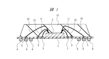
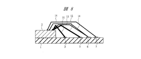
第1主面および第1裏面を有し、前記第1主面において中央部にチップ搭載領域が設けられ、前記チップ搭載領域を囲む第1領域にリング状の複数の第1ボンディング電極が形成され、前記第1領域を囲む第2領域に複数の第2ボンディング電極が形成され、内部に前記第1ボンディング電極および前記第2ボンディング電極と電気的に接続する配線が形成された配線基板と、
第2主面および第2裏面を有し、前記第2裏面が前記チップ搭載領域と接するように前記配線基板に搭載され、前記第2主面において複数の電極が配置された半導体チップと、
前記複数の電極とこれに対応する前記第1ボンディング電極または前記第2ボンディング電極とを電気的に接続する複数のワイヤとを有し、
前記複数の第1ボンディング電極は電源電位もしくは基準電位と電気的に接続し、
前記複数の第2ボンディング電極は信号の入力もしくは出力に用いられ、
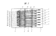
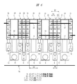
前記複数の電極は、前記第2主面の外周に沿って複数列で配列され、第1列に含まれる前記電極と、前記第2主面内において前記第1列の内側に位置する第2列に含まれる前記電極とは、前記第2主面の前記外周に沿った方向で互い違いに配置され、
前記複数の電極は、前記第1ボンディング電極と電気的に接続される複数の第1電極と、前記複数の第2ボンディング電極と電気的に接続される複数の第2電極とを含み、
(a)前記複数のワイヤのうち、前記第1ボンディング電極と前記複数の第1電極とを電気的に接続する複数の第1ワイヤは、前記複数の第2ボンディング電極と前記複数の第2電極とを電気的に接続する複数の第2ワイヤ以上の径を有する、
もしくは、
(b)1個の前記第1電極と前記第1ボンディング電極との間には、複数の前記ワイヤが接続されている、
を満たすものである。
(a)第1主面および第1裏面を有し、前記第1主面において中央部にチップ搭載領域が設けられ、前記チップ搭載領域を囲む第1領域に電源電位もしくは基準電位と電気的に接続されるリング状の複数の第1ボンディング電極が形成され、前記第1領域を囲む第2領域に信号の入力もしくは出力に用いられる複数の第2ボンディング電極が形成され、内部に前記第1ボンディング電極および前記第2ボンディング電極と電気的に接続する配線が形成された配線基板を用意する工程、
(b)第2主面および第2裏面を有し、前記第2主面において複数の電極が外周に沿って複数列で配置された半導体チップを用意する工程、
(c)前記第2裏面が前記チップ搭載領域と接するように前記半導体チップを前記配線基板に搭載する工程、
(d)前記複数の電極とこれに対応する前記第1ボンディング電極とを第1ワイヤによって電気的に接続する工程、
(e)前記複数の電極とこれに対応する前記第2ボンディング電極とを第2ワイヤによって電気的に接続する工程、
を含み、
前記(b)工程は、
(b1)第1列に含まれる前記電極と、前記第2主面内において前記第1列の内側に位置する第2列に含まれる前記電極とを、前記第2主面の前記外周に沿った方向で互い違いに配置する工程、
を含み、
前記複数の電極は、前記第1ボンディング電極と電気的に接続される複数の第1電極と、前記複数の第2ボンディング電極と電気的に接続される複数の第2電極とを含み、
前記第1ワイヤの径は、前記第2ワイヤの径以上とするものである。
(a)第1主面および第1裏面を有し、前記第1主面において中央部にチップ搭載領域が設けられ、前記チップ搭載領域を囲む第1領域に電源電位もしくは基準電位と電気的に接続されるリング状の複数の第1ボンディング電極が形成され、前記第1領域を囲む第2領域に信号の入力もしくは出力に用いられる複数の第2ボンディング電極が形成され、内部に前記第1ボンディング電極および前記第2ボンディング電極と電気的に接続する配線が形成された配線基板を用意する工程、
(b)第2主面および第2裏面を有し、前記第2主面において複数の電極が外周に沿って複数列で配置された半導体チップを用意する工程、
(c)前記第2裏面が前記チップ搭載領域と接するように前記半導体チップを前記配線基板に搭載する工程、
(d)前記複数の電極とこれに対応する前記第1ボンディング電極または前記第2ボンディング電極とを複数のワイヤによって電気的に接続する工程、
を含み、
前記(b)工程は、
(b1)第1列に含まれる前記電極と、前記第2主面内において前記第1列の内側に位置する第2列に含まれる前記電極とを、前記第2主面の前記外周に沿った方向で互い違いに配置する工程、
を含み、
前記複数の電極は、前記第1ボンディング電極と電気的に接続される複数の第1電極と、前記複数の第2ボンディング電極と電気的に接続される複数の第2電極とを含み、
1個の前記第1電極と前記第1ボンディング電極との間には、前記複数のワイヤを接続するものである。
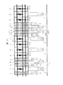
図1は本実施の形態1の半導体装置の構造の一例を示す断面図であり、図2は図1に示した半導体装置の要部平面図であり、図3は図1に示した半導体装置の要部断面図である。
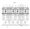
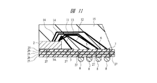
本実施の形態2の半導体装置も前記実施の形態1の半導体装置と同様に、配線基板上にチップが搭載された樹脂封止型の半導体パッケージである。
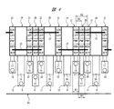
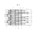
図13は本実施の形態3の半導体装置の要部平面図である。
2 チップ
2A チップ端部
3、5 ボンディング電極(第1ボンディング電極)
3A 電極(第3ボンディング電極)
4A ボンディング電極
4B、4C ボンディング電極(第4ボンディング電極)
6、7 ボンディング電極(第2ボンディング電極)
8 はんだボール
9 ボンディングパッド(電極、第1電極)
10 ボンディングパッド(電極、第2電極)
11、12 ワイヤ(第1ワイヤ)
11A、12A ワイヤ(第1ワイヤ)
13 ワイヤ(第2ワイヤ)
14 ワイヤ(第2ワイヤ)
15 封止体
16 配線
17 配線
18 電源回路セル
19 電源回路セル
20 入出力回路セル
21 入出力回路セル
22、22A、23、23A 配線
25 絶縁層
26 配線(配線層)
27 配線
31 半導体基板
32 p型ウエル
33 n型ウエル
34N、34P ゲート電極
35N、36N n型半導体領域
35P、36P p型半導体領域
37 層間絶縁膜
38A、38B、38C、38D プラグ
39A、39B、39C、39D 配線
41A ボンディングパッド
41B ボンディングパッド
41C ボンディングパッド
42、43 ワイヤ
44 配線
45 内部電源回路セル
46 配線
BUF バッファ回路
D1、D2 ダイオード
ESD 静電破壊保護回路
LEV レベルシフト回路
LOG 論理回路
PBF プリバッファ回路
Qn nチャネル型MISFET
Qp pチャネル型MISFET
Claims (11)
- 第1主面と、前記第1主面と対向する第1裏面と、前記第1主面に設けられたチップ搭載領域と、前記チップ搭載領域の周囲に設けられ、かつ電源電位または接地電位が供給される複数の第1ボンディング電極と、前記第1ボンディング電極よりも前記チップ搭載領域から遠い位置に設けられ、かつ信号が入力または出力される複数の第2ボンディング電極とを含む配線基板と、
第2主面と、前記第2主面と対向する第2裏面と、前記第2主面に設けられ、かつ前記第2主面の外周に沿って設けられた複数の第1電極と、前記第2主面に設けられ、かつ前記複数の第1電極よりも内側に設けられた複数の第2電極と、前記第2主面に設けられ、かつ前記複数の第2電極よりも内側の領域に設けられた複数の電源回路セルと、前記第2主面に設けられ、かつ前記複数の第2電極よりも内側の領域に設けられた複数の入出力回路セルとを含み、前記第2裏面が前記チップ搭載領域と対向するように前記配線基板に搭載された半導体チップと、
前記複数の第1ボンディング電極と前記複数の第1電極をそれぞれ電気的に接続する複数の第1ワイヤと、前記複数の第2ボンディング電極と前記複数の第2電極をそれぞれ電気的に接続する複数の第2ワイヤとを有し、
前記第1電極と前記第2電極は、前記半導体チップの外周に沿った方向で互い違いに配置され、
前記第1電極の外形サイズは、前記第2電極の外形サイズよりも大きく、
前記複数の電源回路セルと前記複数の第1電極を電気的に接続する複数の第1配線の幅は、前記複数の入出力回路セルと前記複数の第2電極を電気的に接続する複数の第2配線の幅よりも太く、
前記複数の電源回路セルは、前記接地電位が供給される第1電源回路セルと、前記電源電位のうちの外部電源電位が供給される第2電源回路セルと、前記電源電位のうちの内部電源電位が供給される第3電源回路セルとを有することを特徴とする半導体装置。 - 請求項1記載の半導体装置において、
前記第1ワイヤの径は、前記第2ワイヤの径よりも太いことを特徴とする半導体装置。 - 請求項1記載の半導体装置において、
前記第1電極に電気的に接続される第1ワイヤの数は、前記第2電極に電気的に接続される第2ワイヤの数よりも多いことを特徴とする半導体装置。 - 請求項1記載の半導体装置において、
前記電源回路セルおよび前記入出力回路セルのそれぞれは、バッファ回路、静電破壊保護回路、プリバッファ回路、レベルシフト回路、および論理回路から形成されていることを特徴とする半導体装置。 - 請求項1記載の半導体装置において、
前記第3電源回路セル上には、第3電極が形成されていることを特徴とする半導体装置。 - 請求項5記載の半導体装置において、
前記複数の第1ボンディング電極は、前記接地電位が供給され、かつ前記チップ搭載領域の周囲にリング状に形成された第3ボンディング電極と、外部電源電位が供給され、かつ前記第3ボンディング電極よりも前記チップ搭載領域から遠い位置にリング状に形成された第4ボンディング電極を有することを特徴とする半導体装置。 - 請求項6記載の半導体装置において、
前記複数の第1ボンディング電極は、更に、前記内部電源電位が供給され、かつ前記第3ボンディング電極と前記第4ボンディング電極との間にリング状に形成された第5ボンディング電極を有することを特徴とする半導体装置。 - 請求項7記載の半導体装置において、
前記第3電極は、前記第5ボンディング電極とそれぞれ電気的に接続されていることを特徴とする半導体装置。 - 請求項1記載の半導体装置において、
前記配線基板は、さらに、前記複数の第1ボンディング電極よりも前記チップ搭載領域から遠い位置に設けられた複数の第6ボンディング電極と、前記複数の第6ボンディング電極よりも前記チップ搭載領域から遠い位置に設けられた複数の第7ボンディング電極を有することを特徴とする半導体装置。 - 請求項9記載の半導体装置において、
前記半導体チップは、さらに、前記半導体チップの前記第2主面の外周に沿って、クロック信号を入力または出力する複数の第4電極を有し、
前記複数の第4電極は、前記複数の第6ボンディング電極と複数の第3ワイヤを介してそれぞれ電気的に接続されていることを特徴とする半導体装置。 - 請求項1記載の半導体装置において、
前記配線基板の前記第1裏面には、複数のはんだボールが設けられ、
前記複数のはんだボールは、前記複数の第1ボンディング電極および前記複数の第2ボンディング電極と複数の配線層を介してそれぞれ電気的に接続されていることを特徴とする半導体装置。
Priority Applications (4)
Application Number | Priority Date | Filing Date | Title |
---|---|---|---|
JP2003433851A JP4570868B2 (ja) | 2003-12-26 | 2003-12-26 | 半導体装置 |
US11/005,217 US7211903B2 (en) | 2003-12-26 | 2004-12-07 | Semiconductor device and manufacturing method of them |
TW93138020A TWI364803B (en) | 2003-12-26 | 2004-12-08 | Semiconductor device |
US11/730,088 US7323788B2 (en) | 2003-12-26 | 2007-03-29 | Semiconductor device and manufacturing method of them |
Applications Claiming Priority (1)
Application Number | Priority Date | Filing Date | Title |
---|---|---|---|
JP2003433851A JP4570868B2 (ja) | 2003-12-26 | 2003-12-26 | 半導体装置 |
Publications (3)
Publication Number | Publication Date |
---|---|
JP2005191447A JP2005191447A (ja) | 2005-07-14 |
JP2005191447A5 JP2005191447A5 (ja) | 2007-02-15 |
JP4570868B2 true JP4570868B2 (ja) | 2010-10-27 |
Family
ID=34791113
Family Applications (1)
Application Number | Title | Priority Date | Filing Date |
---|---|---|---|
JP2003433851A Expired - Fee Related JP4570868B2 (ja) | 2003-12-26 | 2003-12-26 | 半導体装置 |
Country Status (3)
Country | Link |
---|---|
US (2) | US7211903B2 (ja) |
JP (1) | JP4570868B2 (ja) |
TW (1) | TWI364803B (ja) |
Families Citing this family (27)
Publication number | Priority date | Publication date | Assignee | Title |
---|---|---|---|---|
JP4570868B2 (ja) * | 2003-12-26 | 2010-10-27 | ルネサスエレクトロニクス株式会社 | 半導体装置 |
JP2007103423A (ja) * | 2005-09-30 | 2007-04-19 | Renesas Technology Corp | 半導体装置及びその製造方法 |
JP4993929B2 (ja) * | 2006-03-23 | 2012-08-08 | ルネサスエレクトロニクス株式会社 | 半導体集積回路装置 |
US7394164B2 (en) * | 2006-07-28 | 2008-07-01 | Ultra Chip, Inc. | Semiconductor device having bumps in a same row for staggered probing |
US7501709B1 (en) * | 2006-08-25 | 2009-03-10 | Altera Corporation | BGA package with wiring schemes having reduced current loop paths to improve cross talk control and characteristic impedance |
US8922028B2 (en) * | 2007-02-13 | 2014-12-30 | Advanced Semiconductor Engineering, Inc. | Semiconductor package |
JP2010010492A (ja) | 2008-06-27 | 2010-01-14 | Sony Corp | 半導体装置および半導体集積回路 |
JP5395407B2 (ja) * | 2008-11-12 | 2014-01-22 | ルネサスエレクトロニクス株式会社 | 表示装置駆動用半導体集積回路装置および表示装置駆動用半導体集積回路装置の製造方法 |
KR100950511B1 (ko) * | 2009-09-22 | 2010-03-30 | 테세라 리써치 엘엘씨 | 와이어 본딩 및 도전성 기준 소자에 의해 제어되는 임피던스를 포함하는 마이크로전자 어셈블리 |
KR100935854B1 (ko) * | 2009-09-22 | 2010-01-08 | 테세라 리써치 엘엘씨 | 와이어 본딩 및 기준 와이어 본딩에 의해 제어되는 임피던스를 가진 마이크로전자 어셈블리 |
JP5448727B2 (ja) * | 2009-11-05 | 2014-03-19 | ルネサスエレクトロニクス株式会社 | 半導体装置及びその製造方法 |
CN102280425B (zh) | 2010-06-11 | 2014-05-28 | 卡西欧计算机株式会社 | 具备键合引线的半导体器件及其制造方法 |
JP5252027B2 (ja) * | 2010-06-11 | 2013-07-31 | カシオ計算機株式会社 | 半導体装置の製造方法 |
JP5467959B2 (ja) | 2010-07-21 | 2014-04-09 | ルネサスエレクトロニクス株式会社 | 半導体装置 |
US8853708B2 (en) | 2010-09-16 | 2014-10-07 | Tessera, Inc. | Stacked multi-die packages with impedance control |
US8581377B2 (en) | 2010-09-16 | 2013-11-12 | Tessera, Inc. | TSOP with impedance control |
US8786083B2 (en) | 2010-09-16 | 2014-07-22 | Tessera, Inc. | Impedance controlled packages with metal sheet or 2-layer RDL |
US8222725B2 (en) | 2010-09-16 | 2012-07-17 | Tessera, Inc. | Metal can impedance control structure |
US9136197B2 (en) | 2010-09-16 | 2015-09-15 | Tessera, Inc. | Impedence controlled packages with metal sheet or 2-layer RDL |
US8773163B1 (en) | 2012-05-28 | 2014-07-08 | Baysand Inc. | Flexible, space-efficient I/O circuitry for integrated circuits |
US20160307873A1 (en) * | 2015-04-16 | 2016-10-20 | Mediatek Inc. | Bonding pad arrangment design for semiconductor package |
JP6875642B2 (ja) | 2016-04-22 | 2021-05-26 | 株式会社ソシオネクスト | 半導体チップおよびこれを備えた半導体装置 |
JP2018107296A (ja) * | 2016-12-27 | 2018-07-05 | ルネサスエレクトロニクス株式会社 | 半導体装置の製造方法 |
JP7273654B2 (ja) * | 2019-08-09 | 2023-05-15 | ルネサスエレクトロニクス株式会社 | 半導体装置、その製造方法および電子装置 |
US20210287965A1 (en) * | 2020-03-13 | 2021-09-16 | Samsung Electronics Co., Ltd. | Semiconductor device |
US11688686B2 (en) | 2020-07-14 | 2023-06-27 | Samsung Electronics Co., Ltd. | Semiconductor device including an input/output circuit |
CN114220825B (zh) * | 2022-02-22 | 2022-08-23 | 上海天马微电子有限公司 | 发光驱动基板、发光面板及显示装置 |
Citations (10)
Publication number | Priority date | Publication date | Assignee | Title |
---|---|---|---|---|
JPH02196450A (ja) * | 1989-01-25 | 1990-08-03 | Nec Corp | 樹脂封止型半導体装置 |
JPH06112359A (ja) * | 1992-09-30 | 1994-04-22 | Kyocera Corp | 電子部品搭載用回路基板 |
JPH0878458A (ja) * | 1994-08-31 | 1996-03-22 | Oki Electric Ind Co Ltd | 半導体デバイス |
JPH1174303A (ja) * | 1997-06-02 | 1999-03-16 | Sgs Thomson Microelectron Sa | 半導体装置および半導体装置の内部アース線を接続する方法 |
JPH1187399A (ja) * | 1997-09-12 | 1999-03-30 | Oki Electric Ind Co Ltd | 半導体集積回路装置及びそのパッケージ構造 |
JPH11284006A (ja) * | 1998-03-31 | 1999-10-15 | Fujitsu Ltd | 半導体装置 |
JP2000235997A (ja) * | 1999-02-15 | 2000-08-29 | Matsushita Electronics Industry Corp | 半導体装置 |
JP2003133470A (ja) * | 2001-10-19 | 2003-05-09 | Acer Laboratories Inc | アレイ型ボンディングパッドを備える半導体チップおよびそのパッケージ |
JP2003197748A (ja) * | 2001-12-13 | 2003-07-11 | Acer Laboratories Inc | アレー型ボンディングパッドを備える半導体チップの内部回路構造及びその製造方法 |
JP2005277392A (ja) * | 2004-02-24 | 2005-10-06 | Canon Inc | 半導体集積回路装置 |
Family Cites Families (9)
Publication number | Priority date | Publication date | Assignee | Title |
---|---|---|---|---|
JP4071914B2 (ja) | 2000-02-25 | 2008-04-02 | 沖電気工業株式会社 | 半導体素子及びこれを用いた半導体装置 |
US6476506B1 (en) * | 2001-09-28 | 2002-11-05 | Motorola, Inc. | Packaged semiconductor with multiple rows of bond pads and method therefor |
TWM244576U (en) * | 2003-07-16 | 2004-09-21 | Via Tech Inc | Chip package structure |
US6956286B2 (en) * | 2003-08-05 | 2005-10-18 | International Business Machines Corporation | Integrated circuit package with overlapping bond fingers |
JP2005136302A (ja) * | 2003-10-31 | 2005-05-26 | Renesas Technology Corp | 半導体集積回路装置の製造方法 |
JP4570868B2 (ja) * | 2003-12-26 | 2010-10-27 | ルネサスエレクトロニクス株式会社 | 半導体装置 |
JP4438579B2 (ja) * | 2004-09-14 | 2010-03-24 | 株式会社デンソー | センサ装置 |
US7675168B2 (en) * | 2005-02-25 | 2010-03-09 | Agere Systems Inc. | Integrated circuit with staggered differential wire bond pairs |
DE102005009163B4 (de) * | 2005-02-25 | 2013-08-14 | Infineon Technologies Ag | Halbleiterbauteil mit einem Halbleiterchip, der Signalkontaktflächen und Versorgungskontaktflächen aufweist, sowie Verfahren zur Herstellung des Halbleiterbauteils |
-
2003
- 2003-12-26 JP JP2003433851A patent/JP4570868B2/ja not_active Expired - Fee Related
-
2004
- 2004-12-07 US US11/005,217 patent/US7211903B2/en active Active
- 2004-12-08 TW TW93138020A patent/TWI364803B/zh active
-
2007
- 2007-03-29 US US11/730,088 patent/US7323788B2/en active Active
Patent Citations (10)
Publication number | Priority date | Publication date | Assignee | Title |
---|---|---|---|---|
JPH02196450A (ja) * | 1989-01-25 | 1990-08-03 | Nec Corp | 樹脂封止型半導体装置 |
JPH06112359A (ja) * | 1992-09-30 | 1994-04-22 | Kyocera Corp | 電子部品搭載用回路基板 |
JPH0878458A (ja) * | 1994-08-31 | 1996-03-22 | Oki Electric Ind Co Ltd | 半導体デバイス |
JPH1174303A (ja) * | 1997-06-02 | 1999-03-16 | Sgs Thomson Microelectron Sa | 半導体装置および半導体装置の内部アース線を接続する方法 |
JPH1187399A (ja) * | 1997-09-12 | 1999-03-30 | Oki Electric Ind Co Ltd | 半導体集積回路装置及びそのパッケージ構造 |
JPH11284006A (ja) * | 1998-03-31 | 1999-10-15 | Fujitsu Ltd | 半導体装置 |
JP2000235997A (ja) * | 1999-02-15 | 2000-08-29 | Matsushita Electronics Industry Corp | 半導体装置 |
JP2003133470A (ja) * | 2001-10-19 | 2003-05-09 | Acer Laboratories Inc | アレイ型ボンディングパッドを備える半導体チップおよびそのパッケージ |
JP2003197748A (ja) * | 2001-12-13 | 2003-07-11 | Acer Laboratories Inc | アレー型ボンディングパッドを備える半導体チップの内部回路構造及びその製造方法 |
JP2005277392A (ja) * | 2004-02-24 | 2005-10-06 | Canon Inc | 半導体集積回路装置 |
Also Published As
Publication number | Publication date |
---|---|
US7211903B2 (en) | 2007-05-01 |
US20050162880A1 (en) | 2005-07-28 |
TW200531194A (en) | 2005-09-16 |
JP2005191447A (ja) | 2005-07-14 |
US7323788B2 (en) | 2008-01-29 |
US20070170601A1 (en) | 2007-07-26 |
TWI364803B (en) | 2012-05-21 |
Similar Documents
Publication | Publication Date | Title |
---|---|---|
JP4570868B2 (ja) | 半導体装置 | |
JP3657246B2 (ja) | 半導体装置 | |
JP4647594B2 (ja) | 集積回路チップのi/oセル | |
EP1897138B1 (en) | Semiconductor device and mounting structure thereof | |
JP5342154B2 (ja) | 半導体装置の製造方法 | |
US6449169B1 (en) | Ball grid array package with interdigitated power ring and ground ring | |
US9087710B2 (en) | Semiconductor device with stacked semiconductor chips | |
US6781240B2 (en) | Semiconductor package with semiconductor chips stacked therein and method of making the package | |
US9947651B2 (en) | Semiconductor integrated circuit device having an NMOS with a high resistance drain terminal | |
KR101654216B1 (ko) | 반도체장치 및 반도체 집적회로 | |
US20110089561A1 (en) | Semiconductor package and method of manufacturing the same | |
US9087822B2 (en) | Semiconductor device | |
JP2007103423A (ja) | 半導体装置及びその製造方法 | |
US20080006930A1 (en) | Semiconductor package | |
JP4068616B2 (ja) | 半導体装置 | |
JP2005150248A (ja) | 半導体集積回路装置 | |
KR100983409B1 (ko) | 반도체 집적회로장치 | |
US5814892A (en) | Semiconductor die with staggered bond pads | |
US20060081972A1 (en) | Fine pitch grid array type semiconductor device | |
CN111755394B (zh) | 倒装芯片封装 | |
JP4167684B2 (ja) | 半導体集積回路装置とその製造方法及びそのテスト方法 | |
JP2005129605A (ja) | 配線基板及びそれを用いた半導体パッケージ | |
US20100193929A1 (en) | Semiconductor device | |
JP2008085019A (ja) | マクロセルブロック及び半導体装置 | |
JP2010263234A (ja) | 半導体集積回路装置 |
Legal Events
Date | Code | Title | Description |
---|---|---|---|
A521 | Request for written amendment filed |
Free format text: JAPANESE INTERMEDIATE CODE: A523 Effective date: 20061225 |
|
A621 | Written request for application examination |
Free format text: JAPANESE INTERMEDIATE CODE: A621 Effective date: 20061225 |
|
A977 | Report on retrieval |
Free format text: JAPANESE INTERMEDIATE CODE: A971007 Effective date: 20081008 |
|
A131 | Notification of reasons for refusal |
Free format text: JAPANESE INTERMEDIATE CODE: A131 Effective date: 20091104 |
|
A521 | Request for written amendment filed |
Free format text: JAPANESE INTERMEDIATE CODE: A523 Effective date: 20091214 |
|
A711 | Notification of change in applicant |
Free format text: JAPANESE INTERMEDIATE CODE: A712 Effective date: 20100528 |
|
TRDD | Decision of grant or rejection written | ||
A01 | Written decision to grant a patent or to grant a registration (utility model) |
Free format text: JAPANESE INTERMEDIATE CODE: A01 Effective date: 20100727 |
|
A01 | Written decision to grant a patent or to grant a registration (utility model) |
Free format text: JAPANESE INTERMEDIATE CODE: A01 |
|
A61 | First payment of annual fees (during grant procedure) |
Free format text: JAPANESE INTERMEDIATE CODE: A61 Effective date: 20100811 |
|
FPAY | Renewal fee payment (event date is renewal date of database) |
Free format text: PAYMENT UNTIL: 20130820 Year of fee payment: 3 |
|
R150 | Certificate of patent or registration of utility model |
Ref document number: 4570868 Country of ref document: JP Free format text: JAPANESE INTERMEDIATE CODE: R150 Free format text: JAPANESE INTERMEDIATE CODE: R150 |
|
S531 | Written request for registration of change of domicile |
Free format text: JAPANESE INTERMEDIATE CODE: R313531 |
|
R350 | Written notification of registration of transfer |
Free format text: JAPANESE INTERMEDIATE CODE: R350 |
|
LAPS | Cancellation because of no payment of annual fees |