EP0892425A2 - Herstellverfahren für eine Platinmetall-Struktur mittels eines Lift-off-Prozesses - Google Patents
Herstellverfahren für eine Platinmetall-Struktur mittels eines Lift-off-Prozesses Download PDFInfo
- Publication number
- EP0892425A2 EP0892425A2 EP98105612A EP98105612A EP0892425A2 EP 0892425 A2 EP0892425 A2 EP 0892425A2 EP 98105612 A EP98105612 A EP 98105612A EP 98105612 A EP98105612 A EP 98105612A EP 0892425 A2 EP0892425 A2 EP 0892425A2
- Authority
- EP
- European Patent Office
- Prior art keywords
- mask
- layer
- platinum metal
- silicon oxide
- substrate
- Prior art date
- Legal status (The legal status is an assumption and is not a legal conclusion. Google has not performed a legal analysis and makes no representation as to the accuracy of the status listed.)
- Ceased
Links
Images
Classifications
-
- H—ELECTRICITY
- H10—SEMICONDUCTOR DEVICES; ELECTRIC SOLID-STATE DEVICES NOT OTHERWISE PROVIDED FOR
- H10D—INORGANIC ELECTRIC SEMICONDUCTOR DEVICES
- H10D1/00—Resistors, capacitors or inductors
- H10D1/60—Capacitors
- H10D1/68—Capacitors having no potential barriers
- H10D1/692—Electrodes
-
- H—ELECTRICITY
- H10—SEMICONDUCTOR DEVICES; ELECTRIC SOLID-STATE DEVICES NOT OTHERWISE PROVIDED FOR
- H10D—INORGANIC ELECTRIC SEMICONDUCTOR DEVICES
- H10D1/00—Resistors, capacitors or inductors
- H10D1/60—Capacitors
- H10D1/68—Capacitors having no potential barriers
- H10D1/692—Electrodes
- H10D1/694—Electrodes comprising noble metals or noble metal oxides
-
- H—ELECTRICITY
- H10—SEMICONDUCTOR DEVICES; ELECTRIC SOLID-STATE DEVICES NOT OTHERWISE PROVIDED FOR
- H10P—GENERIC PROCESSES OR APPARATUS FOR THE MANUFACTURE OR TREATMENT OF DEVICES COVERED BY CLASS H10
- H10P14/00—Formation of materials, e.g. in the shape of layers or pillars
- H10P14/60—Formation of materials, e.g. in the shape of layers or pillars of insulating materials
- H10P14/69—Inorganic materials
- H10P14/692—Inorganic materials composed of oxides, glassy oxides or oxide-based glasses
- H10P14/6921—Inorganic materials composed of oxides, glassy oxides or oxide-based glasses containing silicon
- H10P14/69215—Inorganic materials composed of oxides, glassy oxides or oxide-based glasses containing silicon the material being a silicon oxide, e.g. SiO2
-
- H—ELECTRICITY
- H10—SEMICONDUCTOR DEVICES; ELECTRIC SOLID-STATE DEVICES NOT OTHERWISE PROVIDED FOR
- H10P—GENERIC PROCESSES OR APPARATUS FOR THE MANUFACTURE OR TREATMENT OF DEVICES COVERED BY CLASS H10
- H10P50/00—Etching of wafers, substrates or parts of devices
- H10P50/20—Dry etching; Plasma etching; Reactive-ion etching
- H10P50/28—Dry etching; Plasma etching; Reactive-ion etching of insulating materials
Definitions
- the invention relates to a manufacturing method for a platinum metal structure on a substrate, especially during manufacture an integrated circuit.
- platinum metals as conductive materials is becoming increasingly interesting in semiconductor technology. Under Platinum metal "is to be understood as the group of platinum metals, ie Pt, Ir, Ru etc. As noble metals they have a high conductivity and do not form non-conductive oxides even at high temperatures in an oxygen-containing atmosphere. Furthermore, they have good interface properties both mechanically and An important area of application of platinum metals is the use as an electrode material for storage capacitors in integrated DRAM memories, in particular if these contain a so-called high- ⁇ dielectric (for example BST) or a ferroelectric as a storage dielectric The production of these storage dielectrics requires high temperatures in an oxidizing atmosphere, and such storage cells require little space and are very interesting for future storage generations.
- high- ⁇ dielectric for example BST
- ferroelectric ferroelectric
- platinum metals are difficult to etch are.
- Previous methods are based mainly on physical Etching, for example ion milling and therefore have low selectivity to other materials, such as for example photoresist. For larger structures too already lift-off with a mask made of photoresist or Titan used.
- a lift-off procedure is carried out under the structuring layer applied a mask to a substrate, the one at the locations of the structure to be created Opening included. Only the part lying on the mask the layer is then removed along with the mask.
- the mask at the edge of the opening is negative Has flank
- the exposed substrate surface is larger than the mask opening at the top of the mask.
- the mask must be overhanging in some form be. This means that the flank is not coated and the solvent for the mask can attack at this point.
- photoresist as a mask in a lift-off procedure are these negative edges only for semiconductor manufacturing unusual special procedures (e.g. Image reversal).
- titanium When using titanium as The time factor plays an important role in the mask, since titanium Contact with air slightly oxidized on the surface and then is difficult to remove.
- the object of the invention is a simple manufacturing process for a structure made of a platinum metal.
- the Manufacturing process should also in the manufacturing process DRAM memory cell can be integrated.
- the invention is based on the use of silicon oxide Part of a mask for a lift-off process. Doing so the required negative edge of the mask according to a first Embodiment achieved by an etching process, in particular through a combination of an anisotropic and a isotropic etching process.
- a silicon layer is applied to the silicon oxide layer and after structuring this double layer accordingly oxidation of the silicon layer of the mask to be produced carried out; the resulting increase in volume Silicon layer leads to an overhang over the silicon oxide layer.
- the silicon oxide mask can be very simple, for example with HF, be removed.
- DRAM memory cell can be integrated, in which an electrode of the Storage capacitor is made of a platinum metal.
- an etch stop layer for example, in front of the silicon oxide layer of silicon nitride to be applied to the Protect removal of the mask.
- Preferred is platinum metal Pt or Ir used.
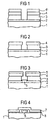
- a substrate 1 is made of nitride, for example Etch stop layer 2, a silicon oxide layer 3 and one Mask layer 4 applied using known methods.
- the thicknesses of layers 2 and 3 can be, for example, 20 nm and 50 nm.
- the substrate can be completed circuit elements included, for example an electrical Connection for the platinum structure to be produced.
- the optional The etch stop layer preferably consists of silicon nitride.
- the Mask layer 4 can either be a photoresist layer, the exposed according to the platinum structure to be produced and is developed so that it can be manufactured in the field Platinum structure has an opening.
- the hard mask 4 can also be one be a so-called hard mask, which consists for example of silicon nitride, and that with the help of an appropriately structured additional Photo mask 4 '(shown in dashed lines) is generated.
- the hard mask 4 after removal the paint mask 4 'used as mask 4.
- the platinum metal also can be sputtered hot.
- the silicon oxide layer 3 etched.
- the oxide layer 3 is initially anisotropic up to the etch stop layer 2 etched.
- the exposed etch stop layer is removed so that the substrate - possibly with a connection structure for the platinum structure - exposed.
- This arrangement is the whole area a platinum metal 5, preferably Pt, for example through a sputtering process.
- the edges of the silicon oxide mask 3 are not coated, so that in subsequent silicon oxide wet etching process to the solvent can attack these places and that on the mask surface overlying platinum is also removed.
- a storage capacitor can pass through Application of a storage dielectric 6, in particular one high ⁇ dielectric or a ferroelectric as explained above, and then producing a second capacitor electrode 7 (also made of platinum, for example) become.
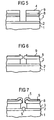
- FIG 5 In the second embodiment, as in the first Embodiment preferably first an etch stop layer 2 applied to the substrate 1. This creates a double layer deposited from silicon oxide 3 and polysilicon 8. Subsequently, an oxidation protection layer 9, in particular a nitride layer. The sequence of layers 3, 8, 9 is then attached using a photo mask 4 an opening in the place of the platinum structure to be produced has anisotropically etched up to the etch stop layer 2. The Paint mask 4 can then be removed.
- a thermal oxidation is carried out the polysilicon at the exposed locations with an increase in volume converted to silicon oxide. This will open up reduced in size in the polysilicon layer 8 and it is formed an overhang over the silicon oxide structure.
- the mask for the The lift-off process here consists of the silicon oxide layer and the polysilicon layer (and possibly the nitride layer).
- the optional oxidation protection layer 9 causes a larger one Overhang, since then the polysilicon 8 only on the exposed Can oxidize edges. In this embodiment In any case, the layout must take into account that due to the oxidation opens up from the original Paint mask 4 is reduced.
- the further process can be done here in the first embodiment be carried out, i.e. it becomes the etch stop layer 2 removed, then applied a platinum metal and that on the Platinum metal on the mask surface together with the Mask removed. As explained, a capacitor can then be used to get finished.
Landscapes
- Semiconductor Memories (AREA)
- Preparing Plates And Mask In Photomechanical Process (AREA)
- Non-Volatile Memory (AREA)
- Electrodes Of Semiconductors (AREA)
- Internal Circuitry In Semiconductor Integrated Circuit Devices (AREA)
- Semiconductor Integrated Circuits (AREA)
Abstract
Description
Claims (9)
- Herstellverfahren für eine Platinmetall-Struktur auf einem Substrat mit folgenden Schritten:a) Aufbringen einer Siliziumoxid-Schicht(3) auf dem Substrat (1)b) Aufbringen einer Maske (4) auf der Siliziumoxidschicht (3), die an der Stelle der herzustellenden Platinmetall-Struktur eine Öffnung aufweist,c) Ätzen der Siliziumoxid-Schicht (3) derart, daß die freigelegte Substratoberfläche größer ist als die Öffnung in der Maske (4),d) Aufbringen einer Platinmetallschicht (5) auf der Maske (4) und der freigelegten Substratoberfläche (1),e) Entfernen der Siliziumoxidschicht (3) in einem Ätzprozeß, so daß das auf der Maske (4) vorhandene Platinmetall (5) mit entfernt wird und das auf der Substratoberfläche vorhandene Platinmetall (5) die Platinmetall-Struktur bildet.
- Verfahren nach Anspruch 1, bei dem Schritt c) einen anisotropen und einen darauffolgenden isotropen Ätzprozeß beinhaltet.
- Verfahren nach einem der Ansprüche 1 und 2, bei dem als Maske (4) eine Hartmaske erzeugt wird.
- Herstellverfahren für eine Platinmetall-Struktur auf einem Substrat (1) mit folgenden Schritten:a) Aufbringen einer Siliziumoxid-Schicht (3) und einer darüberliegenden Siliziumschicht (8) auf dem Substrat (,1),b) Aufbringen einer Fotomaske (4) auf der Siliziumschicht (8), die an der Stelle der herzustellenden Platinmetallstruktur eine Öffnung aufweist,c) Ätzen der Siliziumschicht (8) und der Siliziumoxidschicht (3), und Oxidieren der freiliegenden Oberfläche der Siliziumschicht (8),d) Aufbringen einer Platinmetallschicht (5) auf der Maskenoberfläche und der freigelegten Substratoberfläche,e) Entfernen der Siliziumoxid-Schicht (3) in einem Ätzprozeß, so daß das auf der Maskenoberfläche vorhandene Platinmetall (5) mit entfernt wird und das auf der Substratoberfläche vorhandene Platinmetall die Platinmetall-Struktur ergibt.
- Verfahren nach einem der Ansprüche 1 bis 4, bei dem vor Schritt a) eine Ätzstopschicht (2) auf dem Substrat (1) aufgebracht wird, die vor Schritt d) innerhalb der Öffnung wieder entfernt wird.
- Verfahren nach Anspruch 5, bei dem in Schritt c) die Oberfläche der Ätzstopschicht (2) freigelegt wird und anschließend die Ätzstopschicht (2) anisotrop oder isotrop geätzt wird.
- Verfahren nach einem der Ansprüche 1 bis 6, bei dem die Siliziumoxidschicht in Schritt e) mit HF entfernt wird.
- Verfahren nach einem der Ansprüche 4 bis 7, bei dem auf die Siliziumschicht (8) in Schritt a) eine Oxidationsschutzschicht (9) aufgebracht wird.
- Verwendung des Verfahrens nach einem der Ansprüche 1 bis 8 bei der Herstellung einer Kondensatorelektrode.
Applications Claiming Priority (2)
| Application Number | Priority Date | Filing Date | Title |
|---|---|---|---|
| DE19717363A DE19717363C2 (de) | 1997-04-24 | 1997-04-24 | Herstellverfahren für eine Platinmetall-Struktur mittels eines Lift-off-Prozesses und Verwendung des Herstellverfahrens |
| DE19717363 | 1997-04-24 |
Publications (2)
| Publication Number | Publication Date |
|---|---|
| EP0892425A2 true EP0892425A2 (de) | 1999-01-20 |
| EP0892425A3 EP0892425A3 (de) | 2000-07-19 |
Family
ID=7827644
Family Applications (1)
| Application Number | Title | Priority Date | Filing Date |
|---|---|---|---|
| EP98105612A Ceased EP0892425A3 (de) | 1997-04-24 | 1998-03-27 | Herstellverfahren für eine Platinmetall-Struktur mittels eines Lift-off-Prozesses |
Country Status (6)
| Country | Link |
|---|---|
| US (1) | US6051485A (de) |
| EP (1) | EP0892425A3 (de) |
| JP (1) | JPH10303200A (de) |
| KR (1) | KR100470541B1 (de) |
| DE (1) | DE19717363C2 (de) |
| TW (1) | TW423111B (de) |
Cited By (1)
| Publication number | Priority date | Publication date | Assignee | Title |
|---|---|---|---|---|
| WO2001003166A1 (de) * | 1999-06-29 | 2001-01-11 | Infineon Technologies Ag | Verfahren zur herstellung einer elektrode |
Families Citing this family (11)
| Publication number | Priority date | Publication date | Assignee | Title |
|---|---|---|---|---|
| KR100388683B1 (ko) * | 2001-03-06 | 2003-06-25 | 삼성전자주식회사 | 반도체 장치의 캐패시터 제조 방법 |
| KR100490575B1 (ko) * | 2001-08-03 | 2005-05-17 | 야마하 가부시키가이샤 | 귀금속 박막 패턴 형성방법 |
| JP4410685B2 (ja) * | 2002-12-19 | 2010-02-03 | インターナショナル・ビジネス・マシーンズ・コーポレーション | フィン型fetを形成する方法 |
| US7677696B2 (en) * | 2004-03-31 | 2010-03-16 | Canon Kabushiki Kaisha | Liquid discharge head |
| US7999353B1 (en) * | 2005-04-26 | 2011-08-16 | Northwestern University | Mesoscale pyramids, hole arrays and methods of preparation |
| KR101201972B1 (ko) * | 2006-06-30 | 2012-11-15 | 삼성디스플레이 주식회사 | 박막 트랜지스터 어레이 기판 및 이의 제조 방법 |
| KR100807226B1 (ko) * | 2006-08-21 | 2008-02-28 | 삼성전자주식회사 | 반도체 장치의 제조 방법 |
| JP2010040616A (ja) * | 2008-08-01 | 2010-02-18 | Opnext Japan Inc | 電極形成方法および半導体素子 |
| KR102421575B1 (ko) * | 2017-12-01 | 2022-07-18 | 삼성디스플레이 주식회사 | 유기 발광 표시 장치 및 유기 발광 표시 장치의 제조 방법 |
| KR102812261B1 (ko) * | 2018-11-19 | 2025-05-27 | 삼성디스플레이 주식회사 | 발광 소자 패턴 형성 방법 및 이를 이용한 표시장치 |
| JP2023523680A (ja) | 2020-03-31 | 2023-06-07 | マイクロソフト テクノロジー ライセンシング,エルエルシー | サイドゲート型半導体-超伝導体ハイブリッドデバイス |
Family Cites Families (29)
| Publication number | Priority date | Publication date | Assignee | Title |
|---|---|---|---|---|
| JPS5394767A (en) * | 1977-01-31 | 1978-08-19 | Hitachi Ltd | Manufacture of semiconductor device |
| JPS55154737A (en) * | 1979-05-22 | 1980-12-02 | Chiyou Lsi Gijutsu Kenkyu Kumiai | Method of forming pattern |
| US4283483A (en) * | 1979-07-19 | 1981-08-11 | Hughes Aircraft Company | Process for forming semiconductor devices using electron-sensitive resist patterns with controlled line profiles |
| JPS5811512B2 (ja) * | 1979-07-25 | 1983-03-03 | 超エル・エス・アイ技術研究組合 | パタ−ン形成方法 |
| JPS57183037A (en) * | 1981-05-06 | 1982-11-11 | Nec Corp | Formation of pattern |
| JPS5891640A (ja) * | 1981-11-26 | 1983-05-31 | Toshiba Corp | 半導体装置の製造方法 |
| US4428796A (en) * | 1982-08-02 | 1984-01-31 | Fairchild Camera And Instrument Corporation | Adhesion bond-breaking of lift-off regions on semiconductor structures |
| US4497684A (en) * | 1983-02-22 | 1985-02-05 | Amdahl Corporation | Lift-off process for depositing metal on a substrate |
| US4533624A (en) * | 1983-05-23 | 1985-08-06 | Sperry Corporation | Method of forming a low temperature multilayer photoresist lift-off pattern |
| JPS62120046A (ja) * | 1985-11-20 | 1987-06-01 | Sanyo Electric Co Ltd | 半導体装置の製造方法 |
| IT1190294B (it) * | 1986-02-13 | 1988-02-16 | Selenia Ind Elettroniche | Una struttura di fotopolimero a multistrati (mlr) per la fabbricazione di dispositivi mesfet con gate submicrometrico e con canale incassato (recesse) di lunghezza variabile |
| JPS6315417A (ja) * | 1986-07-08 | 1988-01-22 | Fujitsu Ltd | 半導体装置の製造方法 |
| JPS63175480A (ja) * | 1987-01-14 | 1988-07-19 | Nec Corp | リセス型mesfetの製造方法 |
| JPH01161787A (ja) * | 1987-12-18 | 1989-06-26 | Toshiba Corp | 酸化物超電導膜の加工方法 |
| JPH0269936A (ja) * | 1988-07-28 | 1990-03-08 | Siemens Ag | 半導体材料上の樹脂構造の形成方法 |
| US5024896A (en) * | 1989-07-06 | 1991-06-18 | International Business Machines Corporation | Collimated metal deposition |
| US5053348A (en) * | 1989-12-01 | 1991-10-01 | Hughes Aircraft Company | Fabrication of self-aligned, t-gate hemt |
| JPH04171809A (ja) * | 1990-11-05 | 1992-06-19 | Nec Corp | 半導体装置の製造方法 |
| JP2740050B2 (ja) * | 1991-03-19 | 1998-04-15 | 株式会社東芝 | 溝埋込み配線形成方法 |
| KR920020676A (ko) * | 1991-04-09 | 1992-11-21 | 김광호 | 반도체 장치의 소자분리 방법 |
| US5240878A (en) * | 1991-04-26 | 1993-08-31 | International Business Machines Corporation | Method for forming patterned films on a substrate |
| US5155053A (en) * | 1991-05-28 | 1992-10-13 | Hughes Aircraft Company | Method of forming t-gate structure on microelectronic device substrate |
| US5242534A (en) * | 1992-09-18 | 1993-09-07 | Radiant Technologies | Platinum lift-off process |
| JP3102965B2 (ja) * | 1993-03-12 | 2000-10-23 | 三菱電機株式会社 | 測距装置 |
| JPH06295856A (ja) * | 1993-04-09 | 1994-10-21 | Sumitomo Heavy Ind Ltd | He圧力コントロール方法及び露光装置用圧力コントロール装置 |
| JPH0837233A (ja) * | 1994-07-22 | 1996-02-06 | Rohm Co Ltd | 半導体装置の製造方法 |
| US5554488A (en) * | 1994-07-28 | 1996-09-10 | Northern Telecom Limited | Semiconductor device structure and method of formation thereof |
| JPH08298263A (ja) * | 1995-04-27 | 1996-11-12 | Nec Corp | 半導体装置の製造方法 |
| US5705432A (en) * | 1995-12-01 | 1998-01-06 | Hughes Aircraft Company | Process for providing clean lift-off of sputtered thin film layers |
-
1997
- 1997-04-24 DE DE19717363A patent/DE19717363C2/de not_active Expired - Fee Related
-
1998
- 1998-03-27 EP EP98105612A patent/EP0892425A3/de not_active Ceased
- 1998-04-08 TW TW087105257A patent/TW423111B/zh not_active IP Right Cessation
- 1998-04-21 JP JP10128210A patent/JPH10303200A/ja active Pending
- 1998-04-22 KR KR10-1998-0014293A patent/KR100470541B1/ko not_active Expired - Fee Related
- 1998-04-24 US US09/066,245 patent/US6051485A/en not_active Expired - Lifetime
Cited By (1)
| Publication number | Priority date | Publication date | Assignee | Title |
|---|---|---|---|---|
| WO2001003166A1 (de) * | 1999-06-29 | 2001-01-11 | Infineon Technologies Ag | Verfahren zur herstellung einer elektrode |
Also Published As
| Publication number | Publication date |
|---|---|
| JPH10303200A (ja) | 1998-11-13 |
| US6051485A (en) | 2000-04-18 |
| KR100470541B1 (ko) | 2005-03-16 |
| DE19717363A1 (de) | 1998-10-29 |
| TW423111B (en) | 2001-02-21 |
| DE19717363C2 (de) | 2001-09-06 |
| EP0892425A3 (de) | 2000-07-19 |
| KR19980081598A (ko) | 1998-11-25 |
Similar Documents
| Publication | Publication Date | Title |
|---|---|---|
| DE19638684C2 (de) | Halbleitervorrichtung mit einem Kontaktloch | |
| DE4142469B4 (de) | Verfahren zur Erzeugung und zur Entfernung von temporären Siliziumdioxid-Strukturen | |
| DE4201506C2 (de) | Verfahren zur Herstellung von DRAM-Speicherzellen mit Stapelkondensatoren mit Flossenstruktur | |
| WO2001043171A1 (de) | Verfahren zur herstellung einer hartmaske | |
| DE2723944A1 (de) | Anordnung aus einer strukturierten schicht und einem muster festgelegter dicke und verfahren zu ihrer herstellung | |
| EP0892425A2 (de) | Herstellverfahren für eine Platinmetall-Struktur mittels eines Lift-off-Prozesses | |
| DE60133740T2 (de) | Herstellungsmethode einer integrierten schaltungsstruktur mit leitenden schichten mit grosser innerer oberfläche | |
| DE3402825A1 (de) | Halbleiteranordnung mit isolationsnut und herstellungsverfahren | |
| DE602004008429T2 (de) | Magnettunnelübergang-stapelablagerung in zwei schritten | |
| DE10012198B4 (de) | Zylindrisches Kondensatorbauelement mit innenseitigem HSG-Silicium und Verfahren zu seiner Herstellung | |
| EP0895278A2 (de) | Strukturierungsverfahren | |
| DE19852256B4 (de) | Verfahren zum Ätzen von Platin | |
| WO2000034985A2 (de) | Verfahren zum strukturieren einer metallhaltigen schicht | |
| DE68922085T2 (de) | Halbleiteranordung und Verfahren zum Herstellen einer Halbleiteranordung. | |
| DE19620185C2 (de) | Verfahren zur Herstellung eines Kondensators einer Halbleitereinrichtung | |
| EP0867926A1 (de) | Herstellverfahren für eine Kondensatorelektrode aus einem Platinmetall | |
| DE10312469A1 (de) | Verfahren zum Herstellen einer Halbleiterstruktur | |
| DE10031881A1 (de) | Halbleitereinrichtung und Verfahren zur Herstellung der Halbleitereinrichtung | |
| DE10262115B4 (de) | Integrierte Schaltungsvorrichtung mit einer Vielzahl an gestapelten Kondensatoren, Metall-Isolator-Metall-Kondensator sowie Herstellungsverfahren dafür | |
| EP1277230B1 (de) | Verfahren zur herstellung von kondensatorstrukturen | |
| EP0902461A2 (de) | Verfahren zur Erzeugung von Strukturen mit einem hohen Aspektverhältnis | |
| DE19710491C2 (de) | Herstellungsverfahren für Halbleiterspeichervorrichtung | |
| EP0931342B1 (de) | Eine barrierenfreie halbleiterspeicheranordnungen und deren herstellungsverfahren | |
| DE4200284C2 (de) | Halbleitereinrichtung und Verfahren zu deren Herstellung | |
| DE112006000261B4 (de) | Verfahren zur Herstellung eines kapazitiven Elements mittels Ätzverfahren |
Legal Events
| Date | Code | Title | Description |
|---|---|---|---|
| PUAI | Public reference made under article 153(3) epc to a published international application that has entered the european phase |
Free format text: ORIGINAL CODE: 0009012 |
|
| AK | Designated contracting states |
Kind code of ref document: A2 Designated state(s): DE FR GB IE IT |
|
| AX | Request for extension of the european patent |
Free format text: AL;LT;LV;MK;RO;SI |
|
| PUAL | Search report despatched |
Free format text: ORIGINAL CODE: 0009013 |
|
| AK | Designated contracting states |
Kind code of ref document: A3 Designated state(s): AT BE CH DE DK ES FI FR GB GR IE IT LI LU MC NL PT SE |
|
| AX | Request for extension of the european patent |
Free format text: AL;LT;LV;MK;RO;SI |
|
| 17P | Request for examination filed |
Effective date: 20000818 |
|
| AKX | Designation fees paid |
Free format text: DE FR GB IE IT |
|
| RAP1 | Party data changed (applicant data changed or rights of an application transferred) |
Owner name: INFINEON TECHNOLOGIES AG |
|
| 17Q | First examination report despatched |
Effective date: 20041217 |
|
| STAA | Information on the status of an ep patent application or granted ep patent |
Free format text: STATUS: THE APPLICATION HAS BEEN REFUSED |
|
| 18R | Application refused |
Effective date: 20050723 |