EP0862665B1 - Verfahren zur elektrolytischen abscheidung von metallschichten - Google Patents
Verfahren zur elektrolytischen abscheidung von metallschichten Download PDFInfo
- Publication number
- EP0862665B1 EP0862665B1 EP96939882A EP96939882A EP0862665B1 EP 0862665 B1 EP0862665 B1 EP 0862665B1 EP 96939882 A EP96939882 A EP 96939882A EP 96939882 A EP96939882 A EP 96939882A EP 0862665 B1 EP0862665 B1 EP 0862665B1
- Authority
- EP
- European Patent Office
- Prior art keywords
- current
- metal
- copper
- anodes
- pulse
- Prior art date
- Legal status (The legal status is an assumption and is not a legal conclusion. Google has not performed a legal analysis and makes no representation as to the accuracy of the status listed.)
- Expired - Lifetime
Links
Images

Classifications
-
- C—CHEMISTRY; METALLURGY
- C25—ELECTROLYTIC OR ELECTROPHORETIC PROCESSES; APPARATUS THEREFOR
- C25D—PROCESSES FOR THE ELECTROLYTIC OR ELECTROPHORETIC PRODUCTION OF COATINGS; ELECTROFORMING; APPARATUS THEREFOR
- C25D3/00—Electroplating: Baths therefor
- C25D3/02—Electroplating: Baths therefor from solutions
- C25D3/38—Electroplating: Baths therefor from solutions of copper
-
- C—CHEMISTRY; METALLURGY
- C25—ELECTROLYTIC OR ELECTROPHORETIC PROCESSES; APPARATUS THEREFOR
- C25D—PROCESSES FOR THE ELECTROLYTIC OR ELECTROPHORETIC PRODUCTION OF COATINGS; ELECTROFORMING; APPARATUS THEREFOR
- C25D5/00—Electroplating characterised by the process; Pretreatment or after-treatment of workpieces
- C25D5/18—Electroplating using modulated, pulsed or reversing current
-
- C—CHEMISTRY; METALLURGY
- C25—ELECTROLYTIC OR ELECTROPHORETIC PROCESSES; APPARATUS THEREFOR
- C25D—PROCESSES FOR THE ELECTROLYTIC OR ELECTROPHORETIC PRODUCTION OF COATINGS; ELECTROFORMING; APPARATUS THEREFOR
- C25D5/00—Electroplating characterised by the process; Pretreatment or after-treatment of workpieces
- C25D5/60—Electroplating characterised by the structure or texture of the layers
- C25D5/615—Microstructure of the layers, e.g. mixed structure
- C25D5/617—Crystalline layers
-
- C—CHEMISTRY; METALLURGY
- C25—ELECTROLYTIC OR ELECTROPHORETIC PROCESSES; APPARATUS THEREFOR
- C25D—PROCESSES FOR THE ELECTROLYTIC OR ELECTROPHORETIC PRODUCTION OF COATINGS; ELECTROFORMING; APPARATUS THEREFOR
- C25D5/00—Electroplating characterised by the process; Pretreatment or after-treatment of workpieces
- C25D5/60—Electroplating characterised by the structure or texture of the layers
- C25D5/623—Porosity of the layers
-
- C—CHEMISTRY; METALLURGY
- C25—ELECTROLYTIC OR ELECTROPHORETIC PROCESSES; APPARATUS THEREFOR
- C25D—PROCESSES FOR THE ELECTROLYTIC OR ELECTROPHORETIC PRODUCTION OF COATINGS; ELECTROFORMING; APPARATUS THEREFOR
- C25D5/00—Electroplating characterised by the process; Pretreatment or after-treatment of workpieces
- C25D5/627—Electroplating characterised by the visual appearance of the layers, e.g. colour, brightness or mat appearance
-
- H—ELECTRICITY
- H05—ELECTRIC TECHNIQUES NOT OTHERWISE PROVIDED FOR
- H05K—PRINTED CIRCUITS; CASINGS OR CONSTRUCTIONAL DETAILS OF ELECTRIC APPARATUS; MANUFACTURE OF ASSEMBLAGES OF ELECTRICAL COMPONENTS
- H05K3/00—Apparatus or processes for manufacturing printed circuits
- H05K3/22—Secondary treatment of printed circuits
- H05K3/24—Reinforcing of the conductive pattern
- H05K3/241—Reinforcing of the conductive pattern characterised by the electroplating method; means therefor, e.g. baths or apparatus
-
- Y—GENERAL TAGGING OF NEW TECHNOLOGICAL DEVELOPMENTS; GENERAL TAGGING OF CROSS-SECTIONAL TECHNOLOGIES SPANNING OVER SEVERAL SECTIONS OF THE IPC; TECHNICAL SUBJECTS COVERED BY FORMER USPC CROSS-REFERENCE ART COLLECTIONS [XRACs] AND DIGESTS
- Y10—TECHNICAL SUBJECTS COVERED BY FORMER USPC
- Y10S—TECHNICAL SUBJECTS COVERED BY FORMER USPC CROSS-REFERENCE ART COLLECTIONS [XRACs] AND DIGESTS
- Y10S205/00—Electrolysis: processes, compositions used therein, and methods of preparing the compositions
- Y10S205/92—Electrolytic coating of circuit board or printed circuit, other than selected area coating
Definitions
- the invention relates to a method for the electrolytic deposition of Metal layers with a uniform layer thickness, in particular of Copper layers, certain physical-mechanical and optical properties.
- the additive solution must contain certain additive compounds in small quantities Amounts are added. This is mainly about organic substances that affect gloss formation, leveling, Uniformity of deposition on large areas, avoidance of so-called burns, i.e. Deposition of coarsely crystalline layers, as well as the formation of metal layers with high elongation at break and Impact tensile strength.
- insoluble anodes are, for example, from German patent specification DD 215 589 B5 and the publication DD 261 613 A1 known. Such are also The method is also described in DE 43 44 387 A1. In these Publications is also the addition of compounds from electrochemically reversible redox systems for the deposition solution indicated with which the addition of metal salts to supplement the deposited metal ions should be avoided.
- DE 27 39 427 C2 describes a method for uniform Coating of profiled workpieces described, which tight Have depressions.
- the wells in the Electrolyte solution flows very intensively onto the surface of the workpiece and at the same time an electrical sequence of pulses of 1 ⁇ sec up to 50 ⁇ sec duration with significantly longer pauses in between applied to the workpiece for electrolytic treatment.
- This method is very complex because of the targeted inflow of profiles in workpiece surfaces at least for mass production is not possible or a very high expenditure on equipment required.
- WO-89/07162 A1 describes an electrochemical method for the deposition described by metals, preferably from copper a sulfuric acid copper electrolyte with organic Additive compounds to improve the physical-mechanical Properties, on workpieces, for example circuit boards. For this is alternating current with different lengths cathodic and anodic pulses applied. It is achieved that the layers are on complex shaped workpieces, such as circuit boards, with be deposited more uniform layer thickness. More information on how the problem can be dealt with, different Layer thicknesses by changing the geometric conditions in the electrolytic cell, for example by dissolving the anodes avoid are not given.
- the copper layers are matt, according to the information in the publication in part even brown or orange, and therefore are not made of pure Copper. In this respect, it is surprising that, according to the authors high ductility values, especially high elongation at break and tensile strength can be reached with the specified method. It will however, no sufficiently precise information about the deposition conditions, such as bath composition, temperature of the bath, used anodes, etc.
- EP 0 356 516 A1 describes a device for applying galvanic Coatings disclosed with which, according to the inventors, the physico-mechanical Properties of the coatings can be improved. For this purpose, the amplitude, shape and frequency during the deposition of the currents flowing through the electrolytic bath automatically changed. It is also stated that by measurement and stabilization the current of the galvanic bath during application galvanic coatings also the physical-mechanical Properties are improved.
- EP 0 129 338 B1 describes a method for the electrolytic treatment of the surface of a metal web using graphite electrodes, in which the resolution of the graphite electrodes used as anodes can be avoided by using alternating current with asymmetrical positive and negative half-waves during the electrolytic treatment that the current distribution in the graphite electrode no longer changes and thus constant conditions obtained during electrolysis.
- this document does not provide any information as to how an improvement in the physical-mechanical properties of deposited metal layers and, at the same time, a layer thickness distribution which is as uniform as possible can be achieved over a long service life.
- EP-A-0 402 896 describes an acidic, copper-containing solution for an electrolytic deposition process known for coating printed circuit boards with holes suitable is.
- the solution also contains an organic additive for grain refinement and lightening.
- a transition metal is used to stabilize the additive contain, which can occur in two positive oxidation levels.
- Fe is used to stabilize the additive contain, which can occur in two positive oxidation levels.
- Fe is used to stabilize the additive contain, which can occur in two positive oxidation levels.
- Fe titanium basket with copper parts located therein is disclosed as the anode.
- GB-A-1 396 436 describes a process for the electrolytic production of hard magnetic Layers on non-rigid substrates are known.
- the present invention is therefore based on the problem of avoiding the disadvantages of the methods according to the prior art and, in particular, of finding an economical and simple method for the electrolytic deposition of metal layers, in particular of copper, the metal layers deposited by the method being very good have physical-mechanical and optical properties, for example gloss even on the workpiece surfaces where the metal is deposited with a high current density, high elongation at break even after a long operating period of a deposition bath and the metal layer thicknesses at all points on the surface of the material to be treated, including existing ones fine holes, is almost the same. Furthermore, the physical-mechanical properties of the coatings should meet the highest requirements (including elongation at break and tensile strength), even when using high current densities, for example of at least 6 A / dm 2 of surface to be coated.
- the deposition solution also contains compounds of an electrochemically reversible redox system, through the oxidized form of which the ions of the deposited metal are formed by dissolving the corresponding metal parts, so optically and perfect layers can be achieved in the physico-mechanical properties when using high current densities (for example above 6 A / dm 2 ).
- uniformly high-gloss copper layers can be applied PCBs with fine holes are deposited, which is also a repeated thermal shock treatment in a solder bath (10 seconds each) Immerse in a 288 ° C hot bath and then cool down to room temperature) without cracks in the copper layer form.
- the achievable metal layer distribution in the holes and on the surface of the circuit boards is very good. Thereby it is possible to deposit smaller amounts of metal on the circuit boards than according to known methods, since the required layer thicknesses can be reached more quickly in the holes.
- the measures according to the invention ensure that organic Additive compounds in the deposition solutions for the production of metal layers can be used with specified properties, without decomposing to any significant degree. Special additive mixtures are not required. Furthermore, high cathodic Current density reached. This enables an economical process since the workpieces to be treated are only relatively short in the system have to linger to with a metal layer with given thickness to be coated. It will have a long life of the dimensionally stable, insoluble anodes reached, since only extremely small Amounts of aggressive reaction products are generated on the anodes.
- the current between the polarized as a cathode Workpieces and the anodes are set galvanostatically and modulated in time using suitable means.
- a voltage between the workpieces and the anodes becomes potentiostatic adjusted and the voltage modulated in time, so that sets a current that changes over time.
- the pulse current or pulse voltage method allows for varying Voltages applied to the workpiece or varying currents between the workpiece and the dimensionally stable, insoluble counter electrode set. For example, a pulse current sequence with anodic and cathodic current pulses on the workpieces and, if necessary with breaks in between with the current intensity Zero repeated periodically. With a corresponding setting of a voltage pulse sequence then the current pulse sequence is set.
- the current is the anodic Current pulses set to at least the same value as the current of the cathodic current pulses on the workpieces, preferably on one Value that is two to three times the value of the cathodic Current pulses.
- the duration of an anodic current pulse on the workpieces is, for example between 0.1 milliseconds (msec) and 1 second (sec) set.
- the anodic pulse lengths are preferably 0.3 up to 10 milliseconds.
- the amount of charge Deposition of the metal may be larger than that used for anodizing Redissolution of the metal from the workpiece leads.
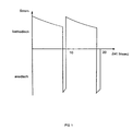
- FIGS. 1 and 2 Typical pulse sequences are shown in FIGS. 1 and 2.
- Figure 1 first a cathodic current pulse with a duration of 9.5 Milliseconds set on the workpiece. This immediately follows an anodic current pulse that is about twice to three times as high Exhibits peak value. This double pulse is at a frequency of 100 Hertz repeated periodically.
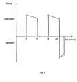
- FIG. 2 shows a pulse sequence which leads to improved results leads.
- the first cathodic phase follows a 5 millisecond long rest phase, in which the current is zero.
- the subsequent cathodic Current pulse lasts 5 milliseconds.
- Then follows again a 5 millisecond rest and then another 5 Millisecond cathodic current pulse. Only then closes a 1 millisecond long anodic current pulse.
- Whose height is only slightly higher than that of the cathodic current pulses.
- the devices that can be used to generate the pulse sequences described can also have several cathodic and / or anodic current pulses can be set with different current levels.
- No soluble anodes from the one to be deposited are used as anodes Metal used, but dimensionally stable, insoluble anodes.
- dimensionally stable, insoluble anodes can be timed a constant distance between the anodes and the workpieces can be set.
- the anodes have the same geometric shape
- Electroplated goods are easily adaptable and change in contrast to soluble anodes their geometric dimensions practically not. This keeps the layer thickness distribution on the surface of the The distance between the anode and cathode which affects the electroplating material constant.
- insoluble anodes are compared to the electrolyte and used in the electrolytic deposition of inert materials, such as stainless steel or lead.
- Anodes which contain titanium or tantalum as base material, preferably with noble metals or oxides of the noble metals is coated. Platinum, iridium or Ruthenium and the oxides or mixed oxides of these metals are used.
- platinum, iridium and ruthenium basically also rhodium, palladium, osmium, silver and gold or whose oxides and mixed oxides are used.
- a particularly high one Resistance to the electrolysis conditions could for example on a titanium anode with an iridium oxide surface, the irradiated with fine particles, for example spherical bodies, and compacted pore-free, can be observed.
- the amount of aggressive reaction products formed at the anode is influenced by the anodic current density. It was found that their formation rate is very small below an anodic current density of 2 A / dm 2 . Therefore, the electrochemically active anode surface must be chosen as large as possible. In order to achieve the largest possible effective anode surfaces with a small spatial limitation, perforated anodes, anode meshes or expanded metal with an appropriate coating are used. This additionally ensures that the anode surfaces can be strongly flowed against by intensive flow through the perforated anode materials.
- this reduces the diffusion layer thickness at the anode, so that only a slight overvoltage arises at the anode, and, on the other hand, the resulting reaction products are quickly removed from the anode surface.
- Nets and expanded metal can also be used in several layers, so that the anode area can be increased even further and the anodic current density can thereby be reduced even further.
- the anode surfaces should also be free of pores that extend down to the base material.
- the separation solution Compounds of an electrochemically reversible redox system added, the oxidized form of the metal ions in a redox reaction the metal parts.
- a metal ion generator in which parts from the to be deposited Metal are included.
- deposition solution depleted of metal ions is transferred to the Anodes passed, with the oxidizing compounds of the redox system form from the reduced form.
- the solution passed through the metal ion generator the oxidizing compounds with the metal parts to form metal ions react.
- the oxidizing compounds of the redox system in the reduced form By forming the Metal ions become the total concentration in the deposition solution contained metal ion concentration kept constant. From The metal ion generator gets the deposition solution back in the electrolyte space in contact with the cathodes and anodes.
- iron (II) - and Iron (III) compounds used as an electrochemically reversible redox system.
- the redox systems are also suitable of the following elements: titanium, cerium, vanadium, manganese and Chrome. You can shape the copper plating solution, for example of titanyl sulfuric acid, cerium (IV) sulfate, sodium metavanadate, Manganese (II) sulfate or sodium chromate can be added. Combined Systems can be advantageous for special applications.
- the effective Fe 2+ / Fe 3+ redox system is formed from the iron (II) sulfate heptahydrate added to the deposition solution. It is ideally suited for aqueous, acidic copper baths.
- Other water-soluble iron salts in particular iron (III) sulfate nonahydrate, can also be used, provided that they do not contain non-biodegradable (hard) complexing agents which can cause problems in the rinsing water disposal (for example iron ammonium alum).
- the use of iron compounds with anions, which lead to undesired side reactions in the copper plating solution, such as chloride or nitrate, must also not be used.
- the concentrations of the compounds of the redox system must be like this be set so that a constant by the dissolution of the metal parts Maintain the concentration of metal ions in the deposition solution can be.
- the inert carrier materials of Anode flaking precious metals or their oxides are not Deposit pieces of copper that may be used in a separate containers and which are under the influence of iron (III) ions be resolved to the copper ion concentration in the Keeping the deposition solution constant.
- this will also Formation of coarse-crystalline metal layers in the high current density range (Burns) avoided.
- the basic composition of a copper bath can vary within relatively wide limits when using the method according to the invention.
- an aqueous solution of the following composition is used (all values in g / liter of separation solution): Copper sulfate (CuSO 4 ⁇ 5 H 2 O) 20-250 preferably 80 - 140 or 180-220 Sulfuric acid, conc. 50-350 preferably 180 - 280 or 50-90 Iron (II) sulfate (FeSO 4 ⁇ 7 H 2 O) 1 - 120 preferably 20-80 Chloride ions (added for example as NaCI) 0.01-0.18 preferably 0.03-0.10.
- copper sulfate instead of copper sulfate, other copper salts can at least partially to be used.
- the sulfuric acid can also be partially or completely replaced by fluoroboric acid, methanesulfonic acid or other acids become.
- the chloride ions are called alkali chloride, for example Sodium chloride, or in the form of hydrochloric acid, p.a. admitted.
- the addition Sodium chloride can be omitted in whole or in part, if in the additives Halide ions are already contained.
- the deposition solution can contain, for example, customary brighteners, Levelers, wetting agents and other additives are added.
- customary brighteners such as nitrogenous sulfur compounds, polymeric nitrogen compounds and / or polymeric phenazonium compounds can also be used.
- the additive compounds are contained in the deposition solution within the following concentration ranges (all values in turn in g / liter of the deposition solution): usual oxygen-containing, high molecular weight compounds 0.005 - 20 preferably usual water soluble 0.01 - 5 organic sulfur compounds 0.0005 - 0.4 preferably 0.001-0.15
- Table 1 shows some oxygen-containing, high-molecular compounds.
- Table 2 shows various sulfur compounds with suitable functional groups for generating water solubility.
- Thiourea derivatives and / or polymeric phenazonium compounds and / or polymeric nitrogen compounds as additive compounds are used in the following concentrations (all values in turn in g / liter of separation solution): 0.0001 - 0.50 preferably 0.0005 - 0.04
- the additive compounds are added to the basic composition given above.
- the conditions for copper deposition are given below: PH value: ⁇ 1 Temperature: 15 ° C - 50 ° C, preferably 25 ° C - 40 ° C cathodic current density: 0.5 - 12 A / dm 2 preferably 3 - 7 A / dm 2
- the separation solution becomes by blowing air into the electrolyte space emotional.
- the convection is increased in the area of the respective surfaces.
- the mass transfer in the vicinity of the cathode or Anode optimized so that higher current densities can be achieved.
- Possibly aggressive oxidizing agents produced in small quantities, such as oxygen and chlorine, are thereby removed from the anodes dissipated.
- Movement of the anodes and cathodes also causes an improved mass transfer on the respective surfaces. Thereby a constant diffusion-controlled deposition is achieved.
- the Movements can be horizontal, vertical, evenly lateral Movement and / or by vibration.
- a combination with the Air flow is particularly effective.
- the metal separation solution is contained in the first container and contains ions of the metal to be deposited on the workpieces and Connections of an electrochemically reversible redox system.
- the workpieces are either arranged in the first container.
- the workpieces and the anodes can also be embodied be arranged outside the container.
- Facilities to promote the separation solution from the first container too to provide the workpieces for example pumps to the Workpieces and the anodes continuously with the deposition solution in To get in touch.
- This arrangement is in a horizontal Continuous flow system as used for the treatment of printed circuit boards can be used.
- Coating systems are usually used in which the Printed circuit boards in a vertical position in a container containing the deposition solution contains, be sunk and in this position arranged on both sides dimensionally stable, insoluble anodes.
- the anodes can through diaphragms from the catholyte space in which the circuit boards be separated.
- diaphragms for example Polypropylene fabric or membranes with a metal ion and Anion permeability, such as Nafion membranes (the DuPont de Nemours Inc., Wilmington, Del., USA).
- the deposition solution is first polarized as the cathode Pumped circuit boards and from there to the anodes.
- this system also includes the copper ion generator into which the anodes coming separation solution arrives. There is the separation solution again enriched with the copper ions.
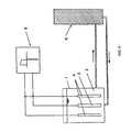
- FIG. 4 A typical arrangement used to treat the workpieces in the Dipping method is suitable, is shown schematically in Figure 4.
- the Container 1 in the Container 1 is the separation solution 2, the connections of the contains electrochemically reversible redox system, for example iron (II) - and iron (III) ions.
- the separation solution can be used, for example Serve copper plating and then contains the previously specified Components.
- the workpieces 3 are immersed in the deposition solution, for example Printed circuit boards, and the anodes 4, for example with iridium oxide coated titanium anodes.
- the workpieces and the anodes are included the power source 5 connected.
- a voltage supply can also be provided for the current source, with the the tension between the workpieces and the anodes is regulated.
- the deposition solution is continually not using shown conveyors, for example pumps, to one second container 6 out.
- the metal ion generator which is supplied by the Through the deposition solution, the metal in the Separation solution added again.
- metallic copper parts for example in Form of pieces, balls or pellets.
- the copper parts loosen the effect of the oxidized form of the redox compounds to copper ions on.
- the oxidized form of the Redox systems converted into the reduced form.
- the ones with copper ions and the reduced form enriched solution is not by means of Pumps shown returned to the first container. That for Metallic copper used for the regeneration does not need phosphorus to contain, but also does not interfere with phosphorus.
- the composition of the anode material In conventional use of soluble copper anodes is the composition of the anode material however, of great importance: In this case, the Copper anodes contain about 0.05 wt .-% phosphorus. Such Materials are expensive and the addition of phosphorus causes residues in the electrolytic cell to remove by additional filtering are.
- Filters for separating can also be placed in the circuit of the separating solution mechanical and / or chemical residues are inserted. However, their need is compared to that of electrolytic cells soluble anodes less because of the addition of phosphorus the anode sludge which arises.
- the circuit boards in horizontal position and horizontal direction of movement through a continuous system transported through.
- the separation solution becomes continuous from below and / or from above through surge nozzles or flood pipes flowed to the circuit boards.
- the anodes are the circuit boards spaced from each other and are like the Printed circuit boards using a suitable device with the deposition solution in Brought in contact.
- the circuit boards are electrically contacted on the side and move on a level that is between the anode levels is arranged through the system.
- the Deposition solution after passing through drill holes in the circuit board means on the side of the circuit board opposite the nozzles arranged devices are suctioned off again.
- the circuit boards are usually contacted electrically using brackets.
- the transport speed in the plant is 0.01 to 2.5 cm / sec, preferably 0.2 - 1.7 cm / sec.
- the circuit boards are made using rollers or Discs transported.
- circuit boards in particular can be used Copper layers on the surfaces and on the already thin Copper metallized surfaces of the holes electrolytically be coated.
- Example 1 (comparative example ):
- An aqueous copper bath with the following composition was used in an electrolysis cell which is provided with soluble, phosphorus-containing copper anodes: Copper sulfate (CuSO 4 ⁇ 5 H 2 O) 80 g / liter, Sulfuric acid, conc. 180 g / liter, Iron (II) sulfate (FeSO 4 ⁇ 7 H 2 O) 35 g / liter, Sodium chloride 0.08 g / liter and the following gloss-forming additive compounds: Polypropylene glycol 1.5 g / liter, 3-mercaptopropan-1-sulfonic acid, sodium salt 0.006 g / liter, N-acetylthiourea 0.001 g / liter.
- a high-gloss copper layer was obtained.
- the metal scatter (Layer thickness in the drill holes x 100 / layer thickness on the circuit board surface) however, was only 55%.
- the elongation of a fraction copper foil deposited from the solution was 21% (measured with the bulge test method with the Ductensiomat according to the DIN ISO method 8401, described in: R. Schulz, D. Nitsche, N. Kanani in: Jahrbuch der mechanicalntechnik, 1992, pages 46 ff.).
- the pulse current sequence according to FIG. 1 contained the following current pulses: Current, cathodic Current density: 4 A / dm 2 Duration: 10 msec, Current, anodic Current density: 8 A / dm 2 Duration: 0.5 msec.
- the metal scatter improved from 55% to 75%.
- none could be used Copper layers are obtained because their appearance was unacceptable.
- the copper layer was only matt.
- the deteriorated Elongation of the copper foil deposited under these conditions from 21% to 14%.
- Example 1 with direct current was repeated. Instead of the soluble, phosphorus-containing copper anodes was coated with mixed oxides Expanded titanium is used as a dimensionally stable, insoluble anode.
- the copper layers deposited were initially uniformly shiny. The physical-mechanical properties were also satisfactory. However, metal scatter values were measured that were below the values given in Example 1. After a long time Operation of the separating bath deteriorated the appearance and the Elongation of the layers. At the same time, it was found that the Mixed oxide coating flaked off the titanium anode. This resulted in that the overvoltage at the anode rose sharply.
- a circuit board provided with copper laminate was in turn electrolytically copper-coated with the electrolyte solution given in Example 1.
- the electrolyte solution given in Example 1 was in turn electrolytically copper-coated with the electrolyte solution given in Example 1.
- soluble copper anodes were used, but a dimensionally stable, insoluble anode.
- a titanium expanded metal coated with mixed oxides served as the anode.
- a concentration of iron (II) sulfate (FeSO 4 .7 H 2 O) of 75 g / liter was set in the deposition solution.
- the deposition solution was pumped from the treatment container into a separate container which was filled with pieces of copper.
- Example 2 Using the pulse current sequence given in Example 2, a uniformly high-gloss copper layer on the circuit board be preserved. The metal scatter deteriorated compared to not in this example and therefore had significantly better values than according to example 1.
- Example 5 The experiment of Example 5 was repeated. However, instead of direct current, a pulse current method according to FIG. 1 was used with the following parameters: Current, cathodic Current density: 6 A / dm 2 Duration: 10 msec, Current, anodic Current density: 10 A / dm 2 Duration: 0.5 msec.
- circuit boards were coated with copper using a platinum-coated titanium expanded metal anode instead of soluble copper anodes. Instead of direct current, a pulse current method with the parameters given in example 6 was used. In addition, the content of iron (II) sulfate (FeSO 4 ⁇ 7H 2 O) in the deposition solution was increased to 80 g / liter.
- the deposited copper layer was uniformly high gloss and thus had a much better appearance than that of the method of Example 5 printed circuit board.
- the circuit board was again a five-time thermal shock test in a 288 C. Solder bath by immersion and cooling in the meantime at room temperature subject. There were no cracks in the copper layer be determined.
- the metal scatter values improved compared to example 6. Values above 85% measured.
- the insoluble anodes were also long-term stable.
Landscapes
- Chemical & Material Sciences (AREA)
- Engineering & Computer Science (AREA)
- Chemical Kinetics & Catalysis (AREA)
- Electrochemistry (AREA)
- Materials Engineering (AREA)
- Metallurgy (AREA)
- Organic Chemistry (AREA)
- Crystallography & Structural Chemistry (AREA)
- Electroplating Methods And Accessories (AREA)
- Electrolytic Production Of Metals (AREA)
- Electroplating And Plating Baths Therefor (AREA)
- Manufacturing Of Printed Wiring (AREA)
Applications Claiming Priority (3)
| Application Number | Priority Date | Filing Date | Title |
|---|---|---|---|
| DE19545231 | 1995-11-21 | ||
| DE19545231A DE19545231A1 (de) | 1995-11-21 | 1995-11-21 | Verfahren zur elektrolytischen Abscheidung von Metallschichten |
| PCT/EP1996/005140 WO1997019206A1 (de) | 1995-11-21 | 1996-11-21 | Verfahren zur elektrolytischen abscheidung von metallschichten |
Publications (2)
| Publication Number | Publication Date |
|---|---|
| EP0862665A1 EP0862665A1 (de) | 1998-09-09 |
| EP0862665B1 true EP0862665B1 (de) | 2000-03-15 |
Family
ID=7779164
Family Applications (1)
| Application Number | Title | Priority Date | Filing Date |
|---|---|---|---|
| EP96939882A Expired - Lifetime EP0862665B1 (de) | 1995-11-21 | 1996-11-21 | Verfahren zur elektrolytischen abscheidung von metallschichten |
Country Status (9)
| Country | Link |
|---|---|
| US (1) | US6099711A (enExample) |
| EP (1) | EP0862665B1 (enExample) |
| JP (2) | JP2000500529A (enExample) |
| AT (1) | ATE190677T1 (enExample) |
| CA (1) | CA2233329C (enExample) |
| DE (2) | DE19545231A1 (enExample) |
| ES (1) | ES2144789T3 (enExample) |
| TW (1) | TW420728B (enExample) |
| WO (1) | WO1997019206A1 (enExample) |
Cited By (1)
| Publication number | Priority date | Publication date | Assignee | Title |
|---|---|---|---|---|
| EP4400634A1 (en) * | 2023-01-13 | 2024-07-17 | Atotech Deutschland GmbH & Co. KG | Process for producing copper foil by electrolytic deposition of copper |
Families Citing this family (85)
| Publication number | Priority date | Publication date | Assignee | Title |
|---|---|---|---|---|
| DE19736350C1 (de) * | 1997-08-21 | 1999-08-05 | Atotech Deutschland Gmbh | Verfahren zur Konzentrationsregulierung von Stoffen in Elektrolyten und Vorrichtung zur Durchführung des Verfahrens |
| US6946065B1 (en) | 1998-10-26 | 2005-09-20 | Novellus Systems, Inc. | Process for electroplating metal into microscopic recessed features |
| US6793796B2 (en) | 1998-10-26 | 2004-09-21 | Novellus Systems, Inc. | Electroplating process for avoiding defects in metal features of integrated circuit devices |
| ATE282248T1 (de) | 1999-01-21 | 2004-11-15 | Atotech Deutschland Gmbh | Verfahren zum galvanischen bilden von leiterstrukturen aus hochreinem kupfer bei der herstellung von integrierten schaltungen |
| DE19915146C1 (de) * | 1999-01-21 | 2000-07-06 | Atotech Deutschland Gmbh | Verfahren zum galvanischen Bilden von Leiterstrukturen aus hochreinem Kupfer bei der Herstellung von integrierten Schaltungen |
| DE19925373B4 (de) * | 1999-06-02 | 2006-04-06 | Robert Bosch Gmbh | Verfahren und Vorrichtung zum Galvanisieren |
| US20040045832A1 (en) * | 1999-10-14 | 2004-03-11 | Nicholas Martyak | Electrolytic copper plating solutions |
| US6294060B1 (en) | 1999-10-21 | 2001-09-25 | Ati Properties, Inc. | Conveyorized electroplating device |
| JP2001267726A (ja) * | 2000-03-22 | 2001-09-28 | Toyota Autom Loom Works Ltd | 配線基板の電解メッキ方法及び配線基板の電解メッキ装置 |
| US6491806B1 (en) | 2000-04-27 | 2002-12-10 | Intel Corporation | Electroplating bath composition |
| NL1015348C2 (nl) * | 2000-05-31 | 2001-12-03 | D R P P B V Dutch Reverse Puls | Methode ter verbetering van electrolytische metaal neerslagverdeling op een substraat met behulp van Periodic Reversal Current waarbij gebruik wordt gemaakt van Oplosbare-, Inerte- en Hybride Anoden. |
| DE10061186C1 (de) * | 2000-12-07 | 2002-01-17 | Astrium Gmbh | Verfahren und Anordnung zur galvanischen Abscheidung von Nickel, Kobalt, Nickellegierungen oder Kobaltlegierungen mit periodischen Strompulsen und Verwendung des Verfahrens |
| US20040060728A1 (en) * | 2001-01-04 | 2004-04-01 | Philippe Steiert | Method for producing electroconductive structures |
| JP2002235189A (ja) * | 2001-02-05 | 2002-08-23 | Sansha Electric Mfg Co Ltd | めっき電流供給電源装置 |
| US6620303B2 (en) * | 2001-05-21 | 2003-09-16 | Hong Kong Polytechnic University | Process for making nickel electroforms |
| US6881318B2 (en) * | 2001-07-26 | 2005-04-19 | Applied Materials, Inc. | Dynamic pulse plating for high aspect ratio features |
| WO2003033775A1 (en) * | 2001-10-16 | 2003-04-24 | Shinko Electric Industries Co., Ltd. | Method of copper-plating small-diameter holes |
| JP2003183879A (ja) * | 2001-12-18 | 2003-07-03 | Learonal Japan Inc | 電解めっき方法 |
| US6919011B2 (en) * | 2001-12-27 | 2005-07-19 | The Hong Kong Polytechnic University | Complex waveform electroplating |
| US7077945B2 (en) * | 2002-03-01 | 2006-07-18 | Northwest Aluminum Technologies | Cu—Ni—Fe anode for use in aluminum producing electrolytic cell |
| US6558525B1 (en) | 2002-03-01 | 2003-05-06 | Northwest Aluminum Technologies | Anode for use in aluminum producing electrolytic cell |
| JP3964263B2 (ja) * | 2002-05-17 | 2007-08-22 | 株式会社デンソー | ブラインドビアホール充填方法及び貫通電極形成方法 |
| US20040134775A1 (en) * | 2002-07-24 | 2004-07-15 | Applied Materials, Inc. | Electrochemical processing cell |
| US7247222B2 (en) * | 2002-07-24 | 2007-07-24 | Applied Materials, Inc. | Electrochemical processing cell |
| US7128823B2 (en) * | 2002-07-24 | 2006-10-31 | Applied Materials, Inc. | Anolyte for copper plating |
| US7223323B2 (en) | 2002-07-24 | 2007-05-29 | Applied Materials, Inc. | Multi-chemistry plating system |
| KR100389061B1 (ko) * | 2002-11-14 | 2003-06-25 | 일진소재산업주식회사 | 전해 동박 제조용 전해액 및 이를 이용한 전해 동박 제조방법 |
| DE10259362A1 (de) * | 2002-12-18 | 2004-07-08 | Siemens Ag | Verfahren zum Abscheiden einer Legierung auf ein Substrat |
| EP1475463B2 (en) † | 2002-12-20 | 2017-03-01 | Shipley Company, L.L.C. | Reverse pulse plating method |
| DE10261493A1 (de) * | 2002-12-23 | 2004-07-08 | METAKEM Gesellschaft für Schichtchemie der Metalle mbH | Anode zur Galvanisierung |
| US20040118691A1 (en) * | 2002-12-23 | 2004-06-24 | Shipley Company, L.L.C. | Electroplating method |
| KR20040073974A (ko) * | 2003-02-14 | 2004-08-21 | 롬 앤드 하스 일렉트로닉 머트어리얼즈, 엘.엘.씨. | 전기도금 조성물 |
| US20050157475A1 (en) * | 2004-01-15 | 2005-07-21 | Endicott Interconnect Technologies, Inc. | Method of making printed circuit board with electroplated conductive through holes and board resulting therefrom |
| US7972491B2 (en) | 2004-04-15 | 2011-07-05 | Hitachi Metals, Ltd. | Method for imparting hydrogen resistance to articles |
| DE602005022650D1 (de) * | 2004-04-26 | 2010-09-16 | Rohm & Haas Elect Mat | Verbessertes Plattierungsverfahren |
| US20050284766A1 (en) * | 2004-06-25 | 2005-12-29 | Herdman Roderick D | Pulse reverse electrolysis of acidic copper electroplating solutions |
| US7329334B2 (en) * | 2004-09-16 | 2008-02-12 | Herdman Roderick D | Controlling the hardness of electrodeposited copper coatings by variation of current profile |
| DE102004045451B4 (de) * | 2004-09-20 | 2007-05-03 | Atotech Deutschland Gmbh | Galvanisches Verfahren zum Füllen von Durchgangslöchern mit Metallen, insbesondere von Leiterplatten mit Kupfer |
| FR2881146B1 (fr) * | 2005-01-27 | 2007-10-19 | Snecma Moteurs Sa | Procede de reparation d'une surface de frottement d'une aube a calage variable de turbomachine |
| JP4799887B2 (ja) * | 2005-03-24 | 2011-10-26 | 石原薬品株式会社 | 電気銅メッキ浴、並びに銅メッキ方法 |
| JP2006283169A (ja) * | 2005-04-04 | 2006-10-19 | Okuno Chem Ind Co Ltd | 酸性電気銅めっき液、及び含硫黄有機化合物の電解消耗量の少ない電気銅めっき方法 |
| EP1712660A1 (de) * | 2005-04-12 | 2006-10-18 | Enthone Inc. | Unlösliche Anode |
| EP1717351A1 (de) * | 2005-04-27 | 2006-11-02 | Enthone Inc. | Galvanikbad |
| DE502005003655D1 (de) * | 2005-05-25 | 2008-05-21 | Enthone | Verfahren und Vorrichtung zur Einstellung der Ionenkonzentration in Elektrolyten |
| US7425255B2 (en) * | 2005-06-07 | 2008-09-16 | Massachusetts Institute Of Technology | Method for producing alloy deposits and controlling the nanostructure thereof using negative current pulsing electro-deposition |
| TWI314957B (en) * | 2005-12-29 | 2009-09-21 | Ind Tech Res Inst | Apparatus for metal plating on a substrate |
| DE502007005345D1 (de) * | 2006-03-30 | 2010-11-25 | Atotech Deutschland Gmbh | Elektrolytisches verfahren zum füllen von löchern und vertiefungen mit metallen |
| US20070278107A1 (en) * | 2006-05-30 | 2007-12-06 | Northwest Aluminum Technologies | Anode for use in aluminum producing electrolytic cell |
| JP2009167506A (ja) * | 2008-01-21 | 2009-07-30 | Ebara Udylite Kk | 酸性電解銅めっき液およびこれを用いる微細配線回路の作製方法 |
| DE102008031003B4 (de) | 2008-06-30 | 2010-04-15 | Siemens Aktiengesellschaft | Verfahren zum Erzeugen einer CNT enthaltenen Schicht aus einer ionischen Flüssigkeit |
| US11225727B2 (en) | 2008-11-07 | 2022-01-18 | Lam Research Corporation | Control of current density in an electroplating apparatus |
| US10011917B2 (en) | 2008-11-07 | 2018-07-03 | Lam Research Corporation | Control of current density in an electroplating apparatus |
| US20100206737A1 (en) * | 2009-02-17 | 2010-08-19 | Preisser Robert F | Process for electrodeposition of copper chip to chip, chip to wafer and wafer to wafer interconnects in through-silicon vias (tsv) |
| US9385035B2 (en) | 2010-05-24 | 2016-07-05 | Novellus Systems, Inc. | Current ramping and current pulsing entry of substrates for electroplating |
| EP2392694A1 (en) | 2010-06-02 | 2011-12-07 | ATOTECH Deutschland GmbH | Method for etching of copper and copper alloys |
| US20120024713A1 (en) | 2010-07-29 | 2012-02-02 | Preisser Robert F | Process for electrodeposition of copper chip to chip, chip to wafer and wafer to wafer interconnects in through-silicon vias (tsv) with heated substrate and cooled electrolyte |
| EP2518187A1 (en) * | 2011-04-26 | 2012-10-31 | Atotech Deutschland GmbH | Aqueous acidic bath for electrolytic deposition of copper |
| US9028666B2 (en) | 2011-05-17 | 2015-05-12 | Novellus Systems, Inc. | Wetting wave front control for reduced air entrapment during wafer entry into electroplating bath |
| CN103179806B (zh) * | 2011-12-21 | 2019-05-28 | 奥特斯有限公司 | 组合的通孔镀覆和孔填充的方法 |
| EP2735627A1 (en) | 2012-11-26 | 2014-05-28 | ATOTECH Deutschland GmbH | Copper plating bath composition |
| JP6035678B2 (ja) * | 2013-02-19 | 2016-11-30 | 住友金属鉱山株式会社 | フレキシブル配線板の製造方法ならびにフレキシブル配線板 |
| JP6411741B2 (ja) * | 2013-05-20 | 2018-10-24 | 国立大学法人 熊本大学 | 電解処理方法及び電解処理装置 |
| EP2865787A1 (en) * | 2013-10-22 | 2015-04-29 | ATOTECH Deutschland GmbH | Copper electroplating method |
| EP3286358B1 (en) | 2015-04-20 | 2019-03-20 | ATOTECH Deutschland GmbH | Electrolytic copper plating bath compositions and a method for their use |
| EP3135709B1 (en) | 2015-08-31 | 2018-01-10 | ATOTECH Deutschland GmbH | Imidazoyl urea polymers and their use in metal or metal alloy plating bath compositions |
| KR102457077B1 (ko) | 2015-08-31 | 2022-10-19 | 아토테크 도이칠란트 게엠베하 운트 콤파니 카게 | 수성 구리 도금 조 및 구리 또는 구리 합금을 기판 상에 침착시키는 방법 |
| ES2681836T3 (es) | 2015-09-10 | 2018-09-17 | Atotech Deutschland Gmbh | Composición de baño para chapado de cobre |
| KR102381803B1 (ko) | 2016-08-15 | 2022-04-01 | 아토테크 도이칠란트 게엠베하 운트 콤파니 카게 | 전해 구리 도금용 산성 수성 조성물 |
| EP3360988B1 (en) | 2017-02-09 | 2019-06-26 | ATOTECH Deutschland GmbH | Pyridinium compounds, a synthesis method therefor, metal or metal alloy plating baths containing said pyridinium compounds and a method for use of said metal or metal alloy plating baths |
| EP3470552B1 (en) | 2017-10-13 | 2020-12-30 | ATOTECH Deutschland GmbH | An acidic aqueous composition for electrolytically depositing a copper deposit |
| ES2800292T3 (es) | 2017-11-09 | 2020-12-29 | Atotech Deutschland Gmbh | Composiciones de electrodeposición para deposición electrolítica de cobre, su uso y un método para depositar electrolíticamente una capa de cobre o aleación de cobre sobre al menos una superficie de un sustrato |
| ES2881029T3 (es) | 2018-01-09 | 2021-11-26 | Atotech Deutschland Gmbh | Aditivo de ureileno, su uso y un método para su preparación |
| EP3511444B1 (en) | 2018-01-16 | 2020-07-22 | ATOTECH Deutschland GmbH | Metal or metal alloy deposition composition and plating compound |
| KR20210020113A (ko) * | 2018-06-15 | 2021-02-23 | 알베르토 토데스칸 | 스테인리스 강 물체를 코팅하기 위한 전해 처리 방법 |
| US11716819B2 (en) * | 2018-06-21 | 2023-08-01 | Averatek Corporation | Asymmetrical electrolytic plating for a conductive pattern |
| JP7087759B2 (ja) * | 2018-07-18 | 2022-06-21 | 住友金属鉱山株式会社 | 銅張積層板 |
| CN112210801A (zh) * | 2019-07-09 | 2021-01-12 | 江西博泉化学有限公司 | 一种用于高纵横比电路板通孔电镀的电镀液及其电镀方法 |
| CN114342569A (zh) | 2019-08-19 | 2022-04-12 | 德国艾托特克有限两合公司 | 高密度互连印刷电路板的制造顺序及高密度互连印刷电路板 |
| KR102875198B1 (ko) * | 2019-08-19 | 2025-10-22 | 아토테크 도이칠란트 게엠베하 운트 콤파니 카게 | 구리로 충전된 마이크로비아들을 포함하는 고밀도 상호연결 인쇄 회로 기판을 제조하는 방법 |
| EP3901331A1 (en) | 2020-04-23 | 2021-10-27 | ATOTECH Deutschland GmbH | Acidic aqueous composition for electrolytically depositing a copper deposit |
| EP3933073B1 (en) | 2020-06-29 | 2023-11-29 | Atotech Deutschland GmbH & Co. KG | Copper electroplating bath |
| US11542626B2 (en) * | 2020-10-08 | 2023-01-03 | Honeywell International Inc. | Systems and methods for enclosed electroplating chambers |
| EP4032930B1 (en) | 2021-01-22 | 2023-08-30 | Atotech Deutschland GmbH & Co. KG | Biuret-based quaternized polymers and their use in metal or metal alloy plating baths |
| CN113106527B (zh) * | 2021-04-19 | 2024-09-10 | 深圳铱创科技有限公司 | 不溶性阳极及脉冲电镀设备 |
| CN120239188B (zh) * | 2025-05-29 | 2025-09-16 | 珠海市航达科技有限公司 | 一种pcb板铜电镀方法 |
Family Cites Families (15)
| Publication number | Priority date | Publication date | Assignee | Title |
|---|---|---|---|---|
| GB1396436A (en) * | 1973-01-08 | 1975-06-04 | Akad Wissenschaften Ddr | Process for the electrolytic production of hard-magnetic layers |
| CH629542A5 (de) * | 1976-09-01 | 1982-04-30 | Inoue Japax Res | Verfahren und vorrichtung zur galvanischen materialablagerung. |
| NL8105150A (nl) * | 1981-11-13 | 1983-06-01 | Veco Beheer Bv | Werkwijze voor het vervaardigen van zeefmateriaal, verkregen zeefmateriaal, alsmede inrichting voor het uitvoeren van de werkwijze. |
| US4468293A (en) * | 1982-03-05 | 1984-08-28 | Olin Corporation | Electrochemical treatment of copper for improving its bond strength |
| JPS58161793A (ja) * | 1982-03-19 | 1983-09-26 | Hitachi Ltd | 連続電気めつき方法 |
| DD215589B5 (de) * | 1983-05-11 | 1994-06-01 | Heinz Dr Rer Nat Liebscher | Verfahren zur elektrolytischen Metallabscheidung bei erzwungener Konvektion |
| JPS59215500A (ja) * | 1983-05-19 | 1984-12-05 | Fuji Photo Film Co Ltd | 電解処理方法 |
| US4808569A (en) * | 1986-10-24 | 1989-02-28 | Gaf Corporation | Fragrance additive |
| JPS63297590A (ja) * | 1987-05-29 | 1988-12-05 | Nagano Pref Gov | 高速電流反転電解によるめつき方法 |
| DD261613A1 (de) * | 1987-06-05 | 1988-11-02 | Leipzig Galvanotechnik | Verfahren zur elektrolytischen kupferabscheidung aus sauren elektrolyten mit dimensionsstabiler anode |
| GB8801827D0 (en) * | 1988-01-27 | 1988-02-24 | Jct Controls Ltd | Improvements in electrochemical processes |
| EP0356516A4 (en) * | 1988-02-23 | 1990-09-26 | Minsky Radiotekhnichesky Institut | Device for applying galvanic coatings |
| GB8913561D0 (en) * | 1989-06-13 | 1989-08-02 | Learonal Uk Plc | Method of stabilising an organic additive in an electroplating solution |
| JPH04320088A (ja) * | 1991-04-18 | 1992-11-10 | Cmk Corp | プリント配線板の製造方法 |
| DE4344387C2 (de) * | 1993-12-24 | 1996-09-05 | Atotech Deutschland Gmbh | Verfahren zur elektrolytischen Abscheidung von Kupfer und Anordnung zur Durchführung des Verfahrens |
-
1995
- 1995-11-21 DE DE19545231A patent/DE19545231A1/de not_active Withdrawn
-
1996
- 1996-11-15 TW TW085113990A patent/TW420728B/zh not_active IP Right Cessation
- 1996-11-21 CA CA002233329A patent/CA2233329C/en not_active Expired - Fee Related
- 1996-11-21 JP JP9519399A patent/JP2000500529A/ja not_active Withdrawn
- 1996-11-21 DE DE59604701T patent/DE59604701D1/de not_active Expired - Lifetime
- 1996-11-21 EP EP96939882A patent/EP0862665B1/de not_active Expired - Lifetime
- 1996-11-21 WO PCT/EP1996/005140 patent/WO1997019206A1/de not_active Ceased
- 1996-11-21 US US09/066,313 patent/US6099711A/en not_active Expired - Lifetime
- 1996-11-21 ES ES96939882T patent/ES2144789T3/es not_active Expired - Lifetime
- 1996-11-21 AT AT96939882T patent/ATE190677T1/de active
-
2009
- 2009-10-02 JP JP2009230437A patent/JP5417112B2/ja not_active Expired - Lifetime
Cited By (2)
| Publication number | Priority date | Publication date | Assignee | Title |
|---|---|---|---|---|
| EP4400634A1 (en) * | 2023-01-13 | 2024-07-17 | Atotech Deutschland GmbH & Co. KG | Process for producing copper foil by electrolytic deposition of copper |
| WO2024149876A1 (en) | 2023-01-13 | 2024-07-18 | Atotech Deutschland GmbH & Co. KG | Process for producing copper foil by electrolytic deposition of copper |
Also Published As
| Publication number | Publication date |
|---|---|
| WO1997019206A1 (de) | 1997-05-29 |
| DE59604701D1 (de) | 2000-04-20 |
| TW420728B (en) | 2001-02-01 |
| EP0862665A1 (de) | 1998-09-09 |
| JP5417112B2 (ja) | 2014-02-12 |
| ES2144789T3 (es) | 2000-06-16 |
| CA2233329A1 (en) | 1997-05-29 |
| ATE190677T1 (de) | 2000-04-15 |
| US6099711A (en) | 2000-08-08 |
| CA2233329C (en) | 2005-07-26 |
| JP2000500529A (ja) | 2000-01-18 |
| JP2009299195A (ja) | 2009-12-24 |
| DE19545231A1 (de) | 1997-05-22 |
Similar Documents
| Publication | Publication Date | Title |
|---|---|---|
| EP0862665B1 (de) | Verfahren zur elektrolytischen abscheidung von metallschichten | |
| EP0944749B1 (de) | Verfahren zur elektrolytischen abscheidung von kupferschichten | |
| DE4344387C2 (de) | Verfahren zur elektrolytischen Abscheidung von Kupfer und Anordnung zur Durchführung des Verfahrens | |
| DE3031501C2 (enExample) | ||
| DE2555834C2 (de) | Verfahren zur elektrolytischen Abscheidung von Chrom | |
| DE3601698C2 (enExample) | ||
| DE3012999C2 (de) | Bad und Verfahren zur galvanischen Abscheidung von hochglänzenden und duktiler Goldlegierungsüberzügen | |
| WO2001029289A1 (de) | Verfahren und vorrichtung zum elektrolytischen behandeln von elektrisch gegeneinander isolierten, elektrisch leitfähigen strukturen auf oberflächen von elektrisch isolierendem folienmaterial sowie anwendungen des verfahrens | |
| DE2208327A1 (de) | Verfahren zur galvanischen Metallplattierung | |
| EP0619386B1 (de) | Elektrolytische Abscheidung von Palladium oder Palladiumlegierungen | |
| AT516876B1 (de) | Abscheidung von dekorativen Palladium-Eisen-Legierungsbeschichtungen auf metallischen Substanzen | |
| CH643004A5 (de) | Mittel fuer die elektrolytische ablagerung von metallischem silber auf ein substrat. | |
| DE102020133188B4 (de) | Verwendung eines Silber-Bismut-Elektrolyt zur Abscheidung von Hartsilberschichten | |
| EP3415665B1 (de) | Verfahren zur galvanischen abscheidung von zink-nickel-legierungsüberzügen aus einem alkalischen zink-nickel-legierungsbad mit reduziertem abbau von additiven | |
| DE2642666A1 (de) | Verfahren und zusammensetzung zur herstellung einer galvanischen abscheidung | |
| DE102011114931B4 (de) | Verfahren zur selektiveren, elektrolytischen Abscheidung von Gold oder einer Goldlegierung | |
| DE102012004348B4 (de) | Verwendung von organischen Thioharnstoffverbindungen zur Erhöhung der galvanischen Abscheiderate von Gold und Goldlegierungen | |
| DE102021002197A1 (de) | Vorrichtung und Verfahren zum Beschichten eines Bauteils oder Halbzeugs mit einer Chromschicht | |
| EP1626098A2 (de) | Verfahren zur Auflösung von Zink in Laugen | |
| DE2743847A1 (de) | Verfahren zur galvanischen abscheidung von nickel und kobalt alleine oder als binaere oder ternaere legierungen | |
| DE2718284A1 (de) | Verfahren und zusammensetzung zur herstellung einer galvanischen abscheidung | |
| EP0341415A1 (de) | Verfahren zum galvanischen Abscheiden eines Zink-Nickel-Legierungsüberzuges auf einem Stahlband | |
| DE10060127B4 (de) | Elektrolytisches Eisenabscheidungsbad und Verfahren zum elektrolytischen Abscheiden von Eisen und Anwendungen des Verfahrens | |
| DD159268A3 (de) | Verfahren zur galvanischen abscheidung von kupferschichten auf leiterplatten | |
| DE102009041250B4 (de) | Verfahren zur elektrolytischen Verkupferung von Zinkdruckguss mit verringerter Neigung zur Blasenbildung |
Legal Events
| Date | Code | Title | Description |
|---|---|---|---|
| PUAI | Public reference made under article 153(3) epc to a published international application that has entered the european phase |
Free format text: ORIGINAL CODE: 0009012 |
|
| 17P | Request for examination filed |
Effective date: 19980320 |
|
| AK | Designated contracting states |
Kind code of ref document: A1 Designated state(s): AT DE ES FR GB IT SE |
|
| GRAG | Despatch of communication of intention to grant |
Free format text: ORIGINAL CODE: EPIDOS AGRA |
|
| 17Q | First examination report despatched |
Effective date: 19990224 |
|
| GRAG | Despatch of communication of intention to grant |
Free format text: ORIGINAL CODE: EPIDOS AGRA |
|
| GRAG | Despatch of communication of intention to grant |
Free format text: ORIGINAL CODE: EPIDOS AGRA |
|
| GRAH | Despatch of communication of intention to grant a patent |
Free format text: ORIGINAL CODE: EPIDOS IGRA |
|
| GRAH | Despatch of communication of intention to grant a patent |
Free format text: ORIGINAL CODE: EPIDOS IGRA |
|
| GRAA | (expected) grant |
Free format text: ORIGINAL CODE: 0009210 |
|
| AK | Designated contracting states |
Kind code of ref document: B1 Designated state(s): AT DE ES FR GB IT SE |
|
| REF | Corresponds to: |
Ref document number: 190677 Country of ref document: AT Date of ref document: 20000415 Kind code of ref document: T |
|
| REF | Corresponds to: |
Ref document number: 59604701 Country of ref document: DE Date of ref document: 20000420 |
|
| ITF | It: translation for a ep patent filed | ||
| GBT | Gb: translation of ep patent filed (gb section 77(6)(a)/1977) |
Effective date: 20000516 |
|
| REG | Reference to a national code |
Ref country code: ES Ref legal event code: FG2A Ref document number: 2144789 Country of ref document: ES Kind code of ref document: T3 |
|
| ET | Fr: translation filed | ||
| PLBE | No opposition filed within time limit |
Free format text: ORIGINAL CODE: 0009261 |
|
| STAA | Information on the status of an ep patent application or granted ep patent |
Free format text: STATUS: NO OPPOSITION FILED WITHIN TIME LIMIT |
|
| 26N | No opposition filed | ||
| REG | Reference to a national code |
Ref country code: GB Ref legal event code: IF02 |
|
| PGFP | Annual fee paid to national office [announced via postgrant information from national office to epo] |
Ref country code: FR Payment date: 20121130 Year of fee payment: 17 |
|
| PGFP | Annual fee paid to national office [announced via postgrant information from national office to epo] |
Ref country code: GB Payment date: 20121120 Year of fee payment: 17 Ref country code: ES Payment date: 20121127 Year of fee payment: 17 Ref country code: SE Payment date: 20121120 Year of fee payment: 17 Ref country code: IT Payment date: 20121123 Year of fee payment: 17 |
|
| PGFP | Annual fee paid to national office [announced via postgrant information from national office to epo] |
Ref country code: AT Payment date: 20131113 Year of fee payment: 18 |
|
| REG | Reference to a national code |
Ref country code: DE Ref legal event code: R082 Ref document number: 59604701 Country of ref document: DE |
|
| REG | Reference to a national code |
Ref country code: SE Ref legal event code: EUG |
|
| GBPC | Gb: european patent ceased through non-payment of renewal fee |
Effective date: 20131121 |
|
| REG | Reference to a national code |
Ref country code: FR Ref legal event code: ST Effective date: 20140731 |
|
| PG25 | Lapsed in a contracting state [announced via postgrant information from national office to epo] |
Ref country code: SE Free format text: LAPSE BECAUSE OF NON-PAYMENT OF DUE FEES Effective date: 20131122 Ref country code: IT Free format text: LAPSE BECAUSE OF NON-PAYMENT OF DUE FEES Effective date: 20131121 |
|
| PG25 | Lapsed in a contracting state [announced via postgrant information from national office to epo] |
Ref country code: GB Free format text: LAPSE BECAUSE OF NON-PAYMENT OF DUE FEES Effective date: 20131121 Ref country code: FR Free format text: LAPSE BECAUSE OF NON-PAYMENT OF DUE FEES Effective date: 20131202 |
|
| PGFP | Annual fee paid to national office [announced via postgrant information from national office to epo] |
Ref country code: DE Payment date: 20141119 Year of fee payment: 19 |
|
| REG | Reference to a national code |
Ref country code: ES Ref legal event code: FD2A Effective date: 20150331 |
|
| PG25 | Lapsed in a contracting state [announced via postgrant information from national office to epo] |
Ref country code: ES Free format text: LAPSE BECAUSE OF NON-PAYMENT OF DUE FEES Effective date: 20131122 |
|
| REG | Reference to a national code |
Ref country code: AT Ref legal event code: MM01 Ref document number: 190677 Country of ref document: AT Kind code of ref document: T Effective date: 20141121 |
|
| PG25 | Lapsed in a contracting state [announced via postgrant information from national office to epo] |
Ref country code: AT Free format text: LAPSE BECAUSE OF NON-PAYMENT OF DUE FEES Effective date: 20141121 |
|
| REG | Reference to a national code |
Ref country code: DE Ref legal event code: R119 Ref document number: 59604701 Country of ref document: DE |
|
| PG25 | Lapsed in a contracting state [announced via postgrant information from national office to epo] |
Ref country code: DE Free format text: LAPSE BECAUSE OF NON-PAYMENT OF DUE FEES Effective date: 20160601 |