EP0862313A2 - Bildein-/ausgabesystem - Google Patents
Bildein-/ausgabesystem Download PDFInfo
- Publication number
- EP0862313A2 EP0862313A2 EP98103396A EP98103396A EP0862313A2 EP 0862313 A2 EP0862313 A2 EP 0862313A2 EP 98103396 A EP98103396 A EP 98103396A EP 98103396 A EP98103396 A EP 98103396A EP 0862313 A2 EP0862313 A2 EP 0862313A2
- Authority
- EP
- European Patent Office
- Prior art keywords
- power supply
- electric power
- image input
- battery
- input device
- Prior art date
- Legal status (The legal status is an assumption and is not a legal conclusion. Google has not performed a legal analysis and makes no representation as to the accuracy of the status listed.)
- Granted
Links
Images


Classifications
-
- H—ELECTRICITY
- H04—ELECTRIC COMMUNICATION TECHNIQUE
- H04N—PICTORIAL COMMUNICATION, e.g. TELEVISION
- H04N1/00—Scanning, transmission or reproduction of documents or the like, e.g. facsimile transmission; Details thereof
- H04N1/00885—Power supply means, e.g. arrangements for the control of power supply to the apparatus or components thereof
- H04N1/00888—Control thereof
- H04N1/00891—Switching on or off, e.g. for saving power when not in use
-
- H—ELECTRICITY
- H04—ELECTRIC COMMUNICATION TECHNIQUE
- H04N—PICTORIAL COMMUNICATION, e.g. TELEVISION
- H04N1/00—Scanning, transmission or reproduction of documents or the like, e.g. facsimile transmission; Details thereof
- H04N1/00885—Power supply means, e.g. arrangements for the control of power supply to the apparatus or components thereof
- H04N1/00899—Detection of supply level or supply failure
-
- H—ELECTRICITY
- H04—ELECTRIC COMMUNICATION TECHNIQUE
- H04N—PICTORIAL COMMUNICATION, e.g. TELEVISION
- H04N1/00—Scanning, transmission or reproduction of documents or the like, e.g. facsimile transmission; Details thereof
- H04N1/00885—Power supply means, e.g. arrangements for the control of power supply to the apparatus or components thereof
- H04N1/00901—Using different supplies or connection to an external supply
-
- H—ELECTRICITY
- H04—ELECTRIC COMMUNICATION TECHNIQUE
- H04N—PICTORIAL COMMUNICATION, e.g. TELEVISION
- H04N1/00—Scanning, transmission or reproduction of documents or the like, e.g. facsimile transmission; Details thereof
- H04N1/00885—Power supply means, e.g. arrangements for the control of power supply to the apparatus or components thereof
- H04N1/00904—Arrangements for supplying power to different circuits or for supplying power at different levels
Definitions
- the present invention relates to an image input device which can be directly connected to an image output device without any intervention of a printer server such as a personal computer and its control method, and an image input/output system.
- a connection between a digital image sensing device and personal computer or a connection between the digital image sensing device and printer upon direct printing is realized by one of wireless and wired methods. Both the methods consume the battery of the digital image sensing device much to transfer data from the digital image sensing device, to check an image on a viewfinder of the digital image sensing device, and so on. That is, upon data transfer to a personal computer or direct printing, the user must connect two cables, i.e., a cable for data transfer and an AC adapter for supplying electric power to the camera.
- the present invention has been made in consideration of the above-mentioned prior art, and has as its object to obviate the need for connecting a power supply line to a digital image sensing device upon data transport and to prevent battery consumption or short battery during the transport.
- the present invention comprises the following arrangement.
- an image input/output system built by connecting an image output device and an image input device, the image output device outputting an image signal received from the image input device, and supplying electric power to the image input device, and the image input device being connected to the image output device via a connection cable to transmit image data to the image output device and to receive the electric power supplied from the image output device, and having a power supply unit, and a power supply control unit for determining whether to receive the electric power from the image output device, for, when it is determined that the image input device can receive the electric power from the image output device, using the electric power from the image output device, and for, when it is determined that the image input device cannot receive the electric power from the image output device, using electric power from the power supply unit.
- an image input device comprising:
- a method of controlling an image input device which has a power supply unit, is connected to an external device, and is driven by electric power supplied from one of the external device and the power supply unit, comprising:
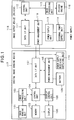
- Fig. 1 is a block diagram of an image input/output system which is built by connecting a digital image sensing device 117 such as a digital camera or the like serving as an image input device, and an image output device 118 such as a printer or the like via an interface such as an IEEE1394 serial bus.
- a digital image sensing device 117 such as a digital camera or the like serving as an image input device
- an image output device 118 such as a printer or the like via an interface such as an IEEE1394 serial bus.
- the present invention will be described hereinafter with reference to this block diagram. This embodiment will exemplify a case wherein the digital image sensing device and printer are directly connected to each other, and the digital image sensing device can receive electric power from the printer.
- the image sensing device 117 obtains a sensed image signal by a CCD in an image sensing unit 101.
- the sensed image signal is subjected to color image processing such as color conversion, filter processing, and the like in an image processing unit 102, and is converted into image data.
- a control unit 104 controls a display control unit 106 to display the image data on a display 105, and stores the image data in a memory 103.
- the control unit 104 controls a power management unit 108 on the basis of information sent from the printer 118 via a data I/F unit 107.
- a recognition signal of a printer, a signal indicating enable/disable of power supply via a connected cable, status of the output device, and the like are received from the printer 118.
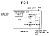
- FIG. 2 shows the arrangement of the power management unit 108.
- a power detection unit 202 measures the power supply capacity supplied from the printer 118, and detects whether to obtain the power supply capacity required for operating the image sensing device 117. When it is confirmed that the power supply capacity from the printer 118 detected by the power detection unit 202 is large enough to operate the digital image sensing device 117, the power supply of the digital image sensing device 117 is switched from a battery 109 to that of the printer 118 obtained via a power supply receiving/supplying unit 110. Also, the power management unit 108 detects the remaining charge on the battery 109. When the remaining charge is small, the power management unit 108 supplies electric power from the power supply receiving/supplying unit 110 to the battery 109 by a switching control unit 201 so as to charge the battery 109.
- the image data is sent to a data I/F unit 111 of the printer 118, and is subjected to processing such as table conversion, RGB ⁇ CMYK conversion, binarization, and the like in an image processing unit 115.
- the processed data is sent to a printer engine 116, and is printed out.
- the digital image sensing device 117 is connected to the printer 118 via a two-way interface to recognize that it is connected to the printer 118 and to determine the power supply capacity supplied from the printer.
- a two-way interface for this purpose, the IEEE1394 standards used in the system of this embodiment will be explained below.
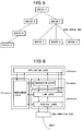
- Fig. 5 shows an example of a network system built using the 1394 serial bus.
- This system comprises devices A, B, C, D, E, F, G, and H, and devices A and B, A and C, B and D, D and E, C and F, C and G, and C and H are connected to each other via 1394 serial bus twisted pair cables.
- These devices A to H are, for example, a PC, digital VTR, DVD, digital camera, hard disk, monitor, and the like.
- connection methods between adjacent devices include both the daisy chain method and node branch method, and connections with a high degree of freedom can be realized.
- the individual devices have their own unique IDs, and recognize each other to build a single network within the range connected via the 1394 serial bus.
- each device serves as a repeater, and constitutes a single network as a whole.
- the 1394 serial bus has a plug-and-play function as its characteristic feature, and when a cable is connected to each device, the device itself and its connection state can be automatically recognized.
- bus reset is automatically done to reset the network configuration used so far and to rebuild a new network.
- the network configuration can always be set and recognized.
- the 1394 serial bus has a data transfer rate of 100/200/400 Mbps, and a device having a higher transfer rate supports the transfer rate of neighboring devices and attains compatibility.
- Data transfer modes include an asynchronous transfer mode for transferring asynchronous data (to be referred to as Async data hereinafter) such as a control signal and the like, and an isochronous transfer mode for transferring isochronous data (to be referred to as Iso data hereinafter) such as real-time video data, audio data, and the like.
- Async data asynchronous transfer mode
- Iso data isochronous transfer mode
- CSP cycle start packet
- Fig. 6 shows the elements of the 1394 serial bus.
- the 1394 serial bus has a layer (hierarchical) structure as a whole. As shown in Fig. 6, the cable of the 1394 serial bus is the lowest hardware layer, the connector of the cable is connected to a connector port, and hardware above the connector port includes the physical layer and link layer.
- the hardware is an actual interface chip.
- the physical layer performs coding and connector control and the like
- the link layer performs packet transfer and cycle time control and the like.
- a transaction layer in firmware manages data to be transferred (transaction), and issues commands such as Read, Write, and the like.
- a management layer manages the connection states and IDs of the devices connected, i.e., manages the network configuration.
- the application layer in software differs depending on the software used, and defines how to interface data.
- the application layer is defined by a protocol such as an AV protocol.
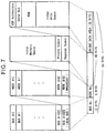
- Fig. 7 shows the address space in the 1394 serial bus.
- Each device (node) connected to the 1394 serial bus must have a unique 64-bit address. By storing this address in a ROM, the sender and receiver addresses in each communication can always be recognized, and a communication with the designated receiver can be made.
- the 1394 address bus is addressed by a method complying with the IEEE1212 standards. Upon setting an address, first 10 bits are used to designate the bus number and the subsequent 6 bits are used to designate the node ID number. The remaining 48 bits are an address width given to each device, and can be used as a unique address space. The last 28 bits store information for identifying each device, designating use conditions, and so on as a unique data area.
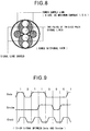
- Fig. 8 is a sectional view of the 1394 serial bus cable.
- connection cable includes a power supply line in addition to two pairs of twisted pair signal lines.
- the prescribed power supply voltage in the power supply line ranges from 8 to 40 V, and the prescribed maximum current is DC 1.5 A.
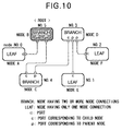
- Fig. 9 is a chart for explaining DS-Link coding of the data transfer format adopted in the 1394 serial bus.
- the 1394 serial bus adopts DS-Link (Data/Strobe Link) coding.
- the DS-Link coding is suitable for high-speed serial communications, and requires two signal lines. That is, one of a twisted pair line sends actual data, and the other sends a strobe signal.
- the receiver side can reproduce clocks by exclusively ORing the received data and strobe signal.
- node IDs are assigned to the individual devices (nodes) connected to recognize them as the network configuration.
- each node that has detected the changes transmits a bus reset signal onto the bus to start a mode for recognizing the new network configuration.
- the change detection method at that time is attained by detecting changes in bias voltage on the 1394 port board.
- the physical layer of each node Upon receiving a bus reset signal transmitted from a certain node, the physical layer of each node informs the link layer of generation of bus reset simultaneously with the reception, and transmits a bus reset signal to another node. After all the nodes have detected the bus reset signal, the bus reset sequence is started.
- the bus reset sequence is started by hardware detection of, e.g., insertion/disinsertion of cables, network abnormality, and the like, and is also started by a command directly issued to the physical layer by, e.g., host control from the protocol.
- each node After the bus reset sequence, each node starts to assign an ID to the individual nodes so as to build a new network configuration.
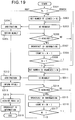
- a general sequence from the bus reset until node ID determination will be explained below with reference to the flow charts in Figs. 17, 18, and 19.
- the flow chart in Fig. 17 shows a series, of bus operations from generation of bus reset until data transfer is ready to restart after determination of the node IDs.
- step S101 the bus reset signal generated in the network is always monitored, and if it is determined in step S101 that the bus reset signal is generated due to, e.g., ON/OFF of the node power switch, the flow advances to step S102.
- step S102 directly connected nodes declare the parent/child relationship so as to recognize the new network connections from the reset state of the network. If it is determined in step S103 that the parent/child relationships are determined among all the nodes, a single root is determined in step S104. Before the parent/child relationships are determined among all the node, the parent/child relationship is repetitively declared in step S102, and no root is determined.
- node IDs are assigned to the individual nodes.
- the node IDs are set in a predetermined node order, and setting is repeated until IDs are assigned to all the nodes. If it is finally determined in step S106 that IDs are set for all the nodes, since a new network configuration has been recognized by all the nodes, data transfer between nodes is ready to restart in step S107, thus restarting data transfer.
- step S107 the control enters the mode for monitoring generation of the bus reset signal again, and upon detecting the bus reset signal, the control repeats the setting operations in steps S101 to S106.
- Fig. 17 has been described.
- Figs. 18 and 19 are flow charts respectively showing the sequence from bus reset until root determination, and the sequence after root determination until IDs are set in more detail, in the flow chart in Fig. 26.
- step S201 If it is determined in step S201 that the bus reset signal is generated, the network configuration is temporarily reset. Note that generation of the bus reset signal is always monitored in step S201.
- step S202 as the first step of the operation for re-recognizing the connections of the reset network, a flag indicating a leaf (node) is set in each device. Furthermore, each device checks the number of nodes connected to its own port in step S203.
- a leaf can declare the parent/child relationship. Whether or not the own node is a leaf can be recognized based on the number of ports detected in step S203. The leaf declares that "the own node is a child, and the node connected is a parent" in step S205, thus ending the operation.
- step S204 If the node recognizes that it has a plurality of ports and is a branch, since the number of undefined ports > 1 is determined in step S204 immediately after bus reset, the flow advances to step S206 to set a flag indicating a branch, and that node waits until it accepts "parent" of the parent/child relationship declared by the leaf in step S207.
- step S207 the branch checks the number of undefined ports in step S204, and if the number of undefined ports is 1, it declares that "the own node is a child" in step S205 with respect to the node connected to the remaining port. After the second checking loop and the subsequent loops, if the number of undefined ports confirmed in step S204 is still 2 or more, the branch waits until it accepts "parent" from the leaf or another branch in step S207.
- step S204 if the number of undefined ports of one branch or, exceptionally, a leaf (if it does not operate quickly although it can declare "child") becomes zero as a result of detection in step S204, it is determined that the parent/child relationships of the entire network have been declared, and a flag indicating a root is set in one and only node, the number of undefined ports of which has become zero (i.e., it is determined as the parent port of all other nodes), in step S208. In step S209, that node is recognized as a root.
- step S302 the number N of leaves (N is a natural number) in the network is set.
- each leaf requests the root ID assignment. If there are more than one assignment requests, the root performs arbitration in step S304, and assigns an ID number to one winning node and informs the losing nodes of the failure result in step S305.
- step S306 the leaf that has failed to acquire an ID issues an ID request again to repeat the above operations.
- the leaf that has acquired an ID broadcasts the acquired ID information to all other nodes in step S307. Upon completion of broadcasting of the ID information from one node, the number of remaining leaves is decremented by 1 in step S308.
- step S310 the number M of branches in the network (M is a natural number) is set. After that, each branch requests ID assignment of the root in step S311.
- the root performs arbitration (for determining one branch) in step S312, and assigns the smallest unassigned ID number next to those assigned to the leaves to one winning branch in step S312.
- step S313 the root informs the branches that issued the requests of ID information or the failure result.
- step S314 each branch that has failed to acquire an ID issues an ID request again to repeat the above operations.
- the branch that has acquired an ID broadcasts the acquired ID information to all other nodes in step S315. Upon completion of broadcasting of the ID information from one node, the number of remaining branches is decremented by 1 in step S316.
- the root since the node that has not acquired ID information yet is only the root, the root sets the smallest unassigned number as its own ID number in step S318, and broadcasts the ID information of the root in step S319.
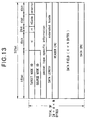
- nodes A and C are directly connected to (root) node B as lower nodes
- node D is directly connected to node C as a lower node
- nodes E and F are directly connected to node D as lower nodes, thus forming a layer structure.
- the layer structure and the sequence for determining the root node and node IDs will be explained below.
- the parent/child relationship is declared between the directly connected ports of the individual nodes.
- the parent is an upper node and the child is a lower node in the layer structure.
- node A declares the parent/child relationship initially.
- the parent/child relationship can be declared in the order from a node having a node connection at only one port (to be referred to as a leaf hereinafter). Since such node can detect first that it has only one port connection, the node recognizes that it is located at the end of the network, and the parent/child relationship is determined in the order from the node that has operated earliest.
- the port of the node which has declared the parent/child relationship e.g., node A between nodes A and B
- node B the port of the node that has accepted the declaration
- the nodes each having a plurality of connected ports (to be referred to as branches hereinafter) declare the parent/child relationships in turn from those that received the parent/child relationships declared by other nodes.
- node D declares the parent/child relationship with respect to node C, and as a result, the child and parent are determined between nodes D and C.
- Node C that received the parent/child relationship declared by node D declares the parent/child relationship with respect to node B connected to the other node thereof. In this way, the child and parent are determined between nodes C and B.
- node B which has become parent nodes at all the connected ports is finally determined to be a root node.
- One and only root node is present in one network configuration.
- node B is determined to be a root node, but another node may be determined if node B that received the parent/child relationship declared by node A declares the parent/child relationship with respect to another node at earlier timing. More specifically, every node may become a root node depending on the transmission timings, and the root node is not always a specific node even in an identical network configuration.
- the mode for determining node IDs is started. In this mode, all the nodes inform all other nodes of their own node IDs determined (broadcast function).
- the own ID information includes the own node number, information of the connected position, the number of ports, the number of connected ports, the parent/child relationships of the individual ports, and the like.
- the node that has acquired an node ID broadcasts information including the node number to other nodes. With this broadcast, it is recognized that the ID number is "already assigned".
- node ID numbers following those of the leaves are assigned to branches.
- the branches that have been assigned node ID numbers broadcast their node ID information in turn in the assignment order, and finally, the root node broadcasts its own ID information. More specifically, the root always have a maximum node ID number.
- the right of accessing the bus is arbitrated prior to data transfer. Since the 1394 serial bus is a logical bus type network in which the connected devices individually relay the transferred signal to send an identical signal to all the devices in the network, arbitration is required to prevent packet collision. With this arbitration, only one node can transfer a signal at a certain timing.
- Fig. 11A shows bus access requests
- Fig. 11B shows a bus access grant. Arbitration will be explained below with reference to Figs. 11A and 11B.
- nodes When arbitration is started, one or a plurality of nodes issue bus access requests to their parent node.
- nodes C and F issue bus access requests.
- the parent node node A in Fig. 11A
- the root node Upon receiving the bus access request, the root node determines the node that is permitted to access the bus. This arbitration can be done by only the root node. The winning node in arbitration is granted bus access. In Fig. 11B, node C is granted bus access, and access by node F is denied. A DP (data prefix) packet is sent to the losing node in arbitration to inform it of denial. The bus access request of the denied node is queued until the next arbitration.
- DP data prefix
- Each node can start data transfer only when the bus is idle. In order to recognize that the previous data transfer has ended and the bus is currently idle, each node determines that it can start data transfer if it detects an elapse of a predetermined idle time gap length (e.g., a subaction gap) set in each transfer mode.
- a predetermined idle time gap length e.g., a subaction gap
- step S401 it is checked if a predetermined gap length according to the data to be transferred such as Async data, Iso data, and the like is obtained. Since the node cannot issue a bus access request required for starting transfer unless the predetermined gap length is obtained, it waits until the predetermined gap length is obtained.
- step S401 If it is determined in step S401 that the predetermined gap length is obtained, it is checked in step S402 if the data to be transferred is present. If such data is present, the node issues a bus access request to the root to assure the bus so as to transfer the data. The bus access request signal is delivered finally to the root while being relayed by the devices in the network, as shown in Fig. 11A. If it is determined in step S402 that the data to be transferred is absent, the control waits for such data.
- step S407 the flow branches depending on one node that is granted access as a result of arbitration of the root from a plurality of nodes that issued access requests, and losing nodes.
- the node starts transfer of the data (packet) to be transferred immediately after reception.
- step S409 the root sends a DP (data prefix) packet indicating an arbitration failure to the nodes that have lost in the arbitration in step S406 and are denied bus access.
- the flow returns to step S401, and the node waits until the predetermined gap length is obtained, so as to issue a bus access request for transferring data again.
- DP data prefix
- asynchronous transfer data are asynchronously transferred.
- Fig. 12 shows progress of asynchronous transfer along with passage of time.
- the first subaction gap in Fig. 12 indicates the idle state of the bus, and when this idle time reaches a predetermined value, the node that wants to transfer data determines that the bus can be used, and executes arbitration for gaining bus control.
- reception acknowledgement send-back code reception acknowledgement send-back code
- the code ack consists of 4-bit information and 4-bit check sum and includes information indicating that data transfer is successful, busy, or pending. The code ack is immediately sent back to the source node.
- Fig. 13 shows an example of the packet format in asynchronous transfer.
- a packet has a header field in addition to a data field and error correction data CRC, and the header field is written with a destination node ID, source node ID, transfer data length, various codes, and the like to transfer the packet.
- Asynchronous transfer is a one-to-one communication from the own node to the destination node.
- the packet transferred from the source node is transferred to all the nodes in the network, but each node ignores a packet with an address other than its own address, and only one destination node can read the packet.
- Isochronous transfer data are transferred isochronously.
- Isochronous transfer as the best feature of the 1394 serial bus is a transfer mode especially suitable for transferring data such as multimedia data (e.g., video data, audio data, and the like) that requires real-time transfer.
- multimedia data e.g., video data, audio data, and the like
- isochronous transfer evenly transfers data from one node to all other nodes by the broadcast function (one-to-many).
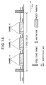
- Fig. 14 shows progress of isochronous transfer along with passage of time.
- the isochronous transfer is executed at predetermined time intervals on the bus. This time interval is called an isochronous cycle.
- the isochronous cycle time is 125 ⁇ s.
- a cycle start packet indicates the start time of each cycle, and has a role of performing time adjustment of the individual nodes.
- a node called a cycle master transmits the cycle start packet.
- the cycle master transmits the cycle start packet indicating the start of the current cycle a predetermined idle period (subaction gap) after the completion of transfer in the previous cycle.
- the transmission time interval of adjacent cycle start packets is 125 ⁇ s.
- a plurality of different packets with different channel IDs can be separately transferred within one cycle.
- a plurality of nodes can attain real-time transfer at the same time, and the receiving node fetches only data with a desired channel ID.
- the channel ID does not represent any destination address but merely assigns a logical number to data. Hence, a certain packet is broadcasted from one source node to all other nodes.
- An iso gap (isochronous gap) shown in Fig. 14 represents an idle period required for recognizing the idle state of the bus before the isochronous transfer. After an elapse of the predetermined idle period, the node which wants to start isochronous transfer determines that the bus is idle, and can perform arbitration before transfer.
- Fig. 15 shows an example of the packet format of isochronous transfer, and the format will be explained below.
- Each of various types of packets assigned to the individual channels has a header field in addition to a data field and error correction data CRC.
- the header field is written with the transfer data length, channel No., various codes, error correction header CRC, and the like, so as to transfer the packet.
- the isochronous transfer has been described.
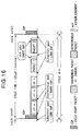
- Fig. 16 shows progress of both isochronous transfer and asynchronous transfer on the bus along with passage of time.
- the isochronous transfer mode is executed prior to the asynchronous transfer mode. This is because the isochronous transfer mode can be started by confirming a gap length (iso gap) shorter than the gap length (subaction gap) required for starting the asynchronous transfer mode. Hence, the isochronous transfer mode is executed prior to the asynchronous transfer mode.
- the cycle start packet is transferred from the cycle master to each individual node at the start timing of cycle #m.
- the individual nodes perform time adjustment, and the node which is to perform isochronous transfer arbitrates after an elapse of a predetermined idle period (iso gap) so as to start packet transfer.
- channels e, s, and k are isochronously transferred in turn.
- isochronous transfer Upon completion of all the isochronous transfer channels in cycle #m after the operation from the arbitration to packet transfer is repeated in correspondence with the number of assigned channels, isochronous transfer is ready to start.
- the node which is to perform asynchronous transfer determines that it can execute arbitration.
- the asynchronous transfer can be performed during only a period wherein the subaction gap for starting asynchronous transfer can be assured from the end of the isochronous transfer until the time (cycle synch) at which the next cycle packet is to be transferred.
- cycle #m In cycle #m in Fig. 16, isochronous transfer for three channels and asynchronous transfer for two packets (packets 1 and 2; including ack) are done. After asynchronous packet 2, since the time (cycle synch) for starting cycle m+1 has been reached, transfer in cycle #m ends.
- the next cycle start packet is transmitted an idle period after the end of that transfer. More specifically, when one cycle continues over 125 ⁇ s, the next cycle is shortened than the reference cycle time of 125 ⁇ s. In this manner, the isochronous cycle can be extended or shortened with reference to 125 ⁇ s.
- the isochronous transfer is executed to maintain real-time transfer every cycle if necessary, and asynchronous transfer may be postponed to the next or subsequent cycle due to the shortened cycle time.
- Fig. 3 is a flow chart showing the actual actions, operations, and processing of the digital image sensing device 117 controlled by the control unit 104 so as to allow better understanding of the above-mentioned actions of the device.
- the digital image sensing device 117 checks if it can receive power supply from the connected cable (step 302).
- the control unit 104 in the digital image sensing device 117 transfers a recognition signal to the printer 118 via the data I/F unit 107, recognizes the printer 118 based on a response signal from the printer 118 with respect to the transferred signal, and checks based on the response signal if the printer 118 can supply power.
- the digital image sensing device 117 cuts off power supply from the internal battery 109 and supplies electric power supplied from the cable connected to the printer 118 to the image sensing device 117 by the switching control unit 201 (step 305). More specifically, the power supply source for operating the digital image sensing device 117 is switched from the internal battery 109 of the image sensing device to electric power supplied via the cable from the power management unit 119 in the printer 118.
- step 306 user's operations are done. For example, the user selects the image to be printed out, determines the output layout, sets the number of sheets to be output, performs processing such as color adjustment, index print, and the like, and prints out the selected image using the digital image sensing device 117 and printer 118.
- the user Upon completion of operations, the user turns off the power switch to turn off the power supply.
- their power switches are interlocked by their power management units 108 and 119.
- the power supplies of both the devices are turned off.
- step 307 both the power supply states of the digital image sensing device 117 and printer 118 are checked.
- a timer 203 in the power management unit 108 starts from the operation end timing, and measures the non-operation time (idling time).
- the power detection unit 202 detects the remaining charge on the battery of the digital image sensing device 117 (step 309). If the remaining charge of the battery is larger than a prescribed value, the power supplies of the digital image sensing device 117 and printer 118 are turned off. However, if the remaining charge on the battery is smaller than the prescribed value, a battery charging mode is started, and the battery is charged by electric power supplied from the printer 118 (step 310).
- step 302 - NO electric power for the digital image sensing device 117 is supplied from the battery 109.
- the remaining capacity of the internal battery 109 of the digital image sensing device is detected in each operation or at a predetermined time interval (step 303). If it is detected that the remaining charge of electric power is not large enough to transfer image data, an alarm for the user, is produced (step 304). This alarm may be displayed on the display 105 of the digital image sensing device 117 or a display (not shown) of the printer 118, or may be printed out onto an output medium of the printer 118. Furthermore, in order to prevent consumption of the battery 109, the digital image sensing device 117 inhibits the power management unit 108 from supplying any electric power to circuit blocks other than the power management unit 108 when no signals are exchanged with the printer 118.
- steps 309 and 310 in Fig. 3 are skipped to inhibit remaining charge detection and charging of the battery 109 of the digital image sensing device 117.
- the power supply is reverted from electric power supplied from the printer 118 to the battery 109.
- the digital image sensing device 117 and printer 118 are connected to each other, and the image sensing device 117 checks if it can receive electric power from the printer 118, and switches the power supply in accordance with the checking result. In this way, by only connecting the digital image sensing device 117 and printer 118, the digital image sensing device 117 can receive electric power from the printer 118. For this reason, battery consumption of the digital image sensing device 117 can be prevented, and the need for an AC power supply can be obviated.
- the digital image sensing device 117 may turn off its power supply to further reduce consumption power.
- Fig. 4 shows the processing flow of the second embodiment.
- This embodiment will be briefly explained below with the aid of this flow chart.
- This embodiment will exemplify a case wherein a digital image sensing device and printer are directly connected to each other, and the digital image sensing device can receive electric power from the printer, as in the first embodiment. Note that the arrangement of the system of this embodiment is the same as that shown in Figs. 1 and 2.
- the digital image sensing device 117 checks if it can receive power supply from the connected cable (step 402). This checking is done in the same manner as in step 302 in Fig. 3.
- the digital image sensing device 117 cuts off power supply from the internal battery 109 and operates its system by electric power supplied from the cable connected to the printer 118 (step 405).
- the digital image sensing device 117 whose drive source is switched from the battery to electric power supplied from the printer 118, detect the electric power amount supplied from the printer 118 using the power detection unit 202 in the power management unit 108 (step 406).
- the detected electric power amount value is sent to the control unit 104 having a CPU (not shown).
- the control unit 104 determines an optimal operation frequency of the CPU that performs arithmetic operations and system control, on the basis of the detected electric power amount value.
- a microprocessor requires more power as its operation frequency rises. For this reason, in a battery driving mode, the operation frequency is set to be lower than that in a driving mode using the power supply from the printer. As a result, the operation frequency of the CPU is changed to that determined by the control unit 104 (step 407).
- the measured electric power amount value is supplied to the display control unit 106 to increase the brightness of the display 105 on the basis of that electric power amount value.
- the display contrast is increased and the visibility of the display 105 can be improved (step 408).
- the display 105 comprises a liquid crystal panel
- the brightness of its backlight is increased when electric power is supplied from the printer 108.
- the printer 108 If electric power cannot be received from the printer 108, if the remaining capacity of the battery 109 is equal to or lower than a predetermined value, the user is informed of such state by means of an alarm display on the display 105 of the digital image sensing device 117 or a printout from the printer 118. On the other hand, if the battery has a sufficiently large remaining capacity, the device is kept operated using the battery 109 as a power supply.
- step 409 are substantially the same as those after step 307 in the first embodiment.
- the digital image sensing device 117 reverts its power supply to the battery 109, drops the driving frequency of the CPU, and reduces the brightness of the display 105 to attain power savings.
- one of two cables i.e., a data transfer cable and power supply cable can be combined to a single cable, and the need for connection of the cable upon direct printing can be obviated.
- the battery can be charged using electric power supplied from the printer.
- functions limited due to problems associated with power consumption e.g., the brightness of the screen of the display, the internal image processing operation speed of the digital image sensing device, and the like, can be improved.
- the need for connection of a power supply line to the digital image sensing device can be obviated, and battery consumption and short battery during data transfer can be prevented.
- the present invention may be applied to either a system constituted by a plurality of equipments (e.g., a host computer, an interface device, a reader, a printer, and the like), or an apparatus consisting of a single equipment (e.g., a copying machine, a facsimile apparatus, or the like).
- equipments e.g., a host computer, an interface device, a reader, a printer, and the like
- an apparatus consisting of a single equipment e.g., a copying machine, a facsimile apparatus, or the like.
- the objects of the present invention are also achieved by supplying a storage medium, which records a program code of a software program that can realize the functions of the above-mentioned embodiments to the system or apparatus, and reading out and executing the program code stored in the storage medium by a computer (or a CPU or MPU) of the system or apparatus.
- the program code itself read out from the storage medium realizes the functions of the above-mentioned embodiments, and the storage medium which stores the program code constitutes the present invention.
- the storage medium for supplying the program code for example, a floppy disk, hard disk, optical disk, magneto-optical disk, CD-ROM, CD-R, magnetic tape, nonvolatile memory card, ROM, and the like may be used.
- the functions of the above-mentioned embodiments may be realized not only by executing the readout program code by the computer but also by some or all of actual processing operations executed by an OS (operating system) running on the computer on the basis of an instruction of the program code.
- OS operating system
- the functions of the above-mentioned embodiments may be realized by some or all of actual processing operations executed by a CPU or the like arranged in a function extension board or a function extension unit, which is inserted in or connected to the computer, after the program code read out from the storage medium is written in a memory of the extension board or unit.
- a power supply for an image sensing device is obtained from a printer to prevent consumption of the battery.
- a power management unit checks if electric power can be supplied from the printer.
- the power management unit switches the power supply from the battery to a power supply receiving/supplying unit that receives electric power from the printer. In this case, if the remaining capacity on the battery is small, the battery is charged by electric power from the printer. Also, the luminance of a display unit is increased, or the operation frequency of a control unit is raised.
- the power management unit switches the power supply to the battery. In this case, the power management unit reduces consumption power by decreasing the luminance of the display unit or reducing the operation frequency of the control unit.
Landscapes
- Engineering & Computer Science (AREA)
- Multimedia (AREA)
- Signal Processing (AREA)
- Accessory Devices And Overall Control Thereof (AREA)
- Facsimiles In General (AREA)
- Power Sources (AREA)
- Information Transfer Systems (AREA)
- Studio Devices (AREA)
Applications Claiming Priority (2)
| Application Number | Priority Date | Filing Date | Title |
|---|---|---|---|
| JP46637/97 | 1997-02-28 | ||
| JP9046637A JPH10243327A (ja) | 1997-02-28 | 1997-02-28 | 画像入力装置とその制御方法及び画像入出力システム |
Publications (3)
| Publication Number | Publication Date |
|---|---|
| EP0862313A2 true EP0862313A2 (de) | 1998-09-02 |
| EP0862313A3 EP0862313A3 (de) | 1998-10-28 |
| EP0862313B1 EP0862313B1 (de) | 2006-10-18 |
Family
ID=12752825
Family Applications (1)
| Application Number | Title | Priority Date | Filing Date |
|---|---|---|---|
| EP98103396A Expired - Lifetime EP0862313B1 (de) | 1997-02-28 | 1998-02-26 | Bildein-/ausgabesystem |
Country Status (4)
| Country | Link |
|---|---|
| US (1) | US6580460B1 (de) |
| EP (1) | EP0862313B1 (de) |
| JP (1) | JPH10243327A (de) |
| DE (1) | DE69836160T2 (de) |
Cited By (10)
| Publication number | Priority date | Publication date | Assignee | Title |
|---|---|---|---|---|
| EP0923035A2 (de) * | 1997-12-09 | 1999-06-16 | Nec Corporation | Kodierschaltung und Verfahren zum Erkennen von Blokcodegrenzen und Herstellen der Synchronization zwischen Verwürfler und Entwürfler |
| EP0924593A2 (de) * | 1997-12-17 | 1999-06-23 | Canon Kabushiki Kaisha | System und Verfahren zur Leistungsregelung |
| EP1178667A2 (de) * | 2000-08-02 | 2002-02-06 | Canon Kabushiki Kaisha | Bildlesevorrichtung und Steuerverfahren |
| EP1295473A1 (de) * | 2000-06-27 | 2003-03-26 | Thomson Licensing S.A. | Multimediengerät zum empfang einer audio-visuellen übertragung |
| WO2004102955A1 (ja) | 2003-05-19 | 2004-11-25 | Sony Corporation | 撮像装置 |
| US6831683B2 (en) | 2001-11-22 | 2004-12-14 | Canon Kabushiki Kaisha | Methods and apparatus for print control of moving a position of a non-print area |
| WO2006120615A2 (en) * | 2005-05-10 | 2006-11-16 | Nxp B.V. | A system and method for transmitting data |
| US7310156B2 (en) | 2001-02-01 | 2007-12-18 | Canon Kabushiki Kaisha | Printing system, printing method, digital camera, storage medium and program for printing method, and printing control apparatus |
| US7550877B2 (en) | 2002-03-20 | 2009-06-23 | Sony Corporation | Electronic apparatus and power supply controlling method |
| US8493450B2 (en) | 2001-02-07 | 2013-07-23 | Canon Kabushiki Kaisha | Camera, printer, print system, control method, memory medium and program therefor |
Families Citing this family (45)
| Publication number | Priority date | Publication date | Assignee | Title |
|---|---|---|---|---|
| JP4127732B2 (ja) * | 1998-07-10 | 2008-07-30 | オリンパス株式会社 | 撮像装置 |
| JP3357005B2 (ja) * | 1999-02-08 | 2002-12-16 | オリンパス光学工業株式会社 | 電子カメラ、画像印刷機構、及び画像印刷機構の電源残量判断方法 |
| JP3357004B2 (ja) * | 1999-02-08 | 2002-12-16 | オリンパス光学工業株式会社 | 電子カメラ |
| JP2000253303A (ja) * | 1999-02-26 | 2000-09-14 | Minolta Co Ltd | 電池駆動されるデジタルカメラ及び電子機器 |
| US7016595B1 (en) * | 1999-05-28 | 2006-03-21 | Nikon Corporation | Television set capable of controlling external device and image storage controlled by television set |
| US7479983B2 (en) * | 2000-03-06 | 2009-01-20 | Sony Corporation | System and method for effectively implementing an electronic image hub device |
| JP2001320620A (ja) * | 2000-05-12 | 2001-11-16 | Canon Inc | 撮像装置及びその制御方法並びに記憶媒体 |
| US7403232B1 (en) * | 2000-09-01 | 2008-07-22 | Eastman Kodak Company | Intelligent power management system |
| JP2002095181A (ja) * | 2000-09-12 | 2002-03-29 | Canon Inc | 複合システム |
| JP2002094873A (ja) * | 2000-09-14 | 2002-03-29 | Fuji Photo Film Co Ltd | デジタルカメラ |
| JP3898889B2 (ja) * | 2000-12-19 | 2007-03-28 | ペンタックス株式会社 | 電源補助ユニット及び携帯機器システム |
| JP4416315B2 (ja) * | 2000-12-21 | 2010-02-17 | キヤノン株式会社 | 撮影装置、及び撮影装置の制御方法 |
| JP2002344794A (ja) * | 2001-05-18 | 2002-11-29 | Fuji Photo Film Co Ltd | デジタルカメラ |
| JP4593834B2 (ja) | 2001-07-02 | 2010-12-08 | 富士フイルム株式会社 | デジタルカメラ及びそのシステム |
| WO2003036777A1 (en) * | 2001-10-22 | 2003-05-01 | Apple Computer, Inc. | Methods and apparatus for charging a battery in a peripheral device |
| US7460170B2 (en) * | 2002-09-23 | 2008-12-02 | Hand Held Products, Inc. | Computer expansion module having image capture and decoding functionality |
| JP4112341B2 (ja) * | 2002-11-20 | 2008-07-02 | オリンパス株式会社 | プリントシステム並びにこのシステムに適合するデジタルカメラ |
| JP3730614B2 (ja) * | 2002-11-26 | 2006-01-05 | 株式会社東芝 | 電子機器における電源制御方法及び電力管理システム |
| JP4502360B2 (ja) * | 2003-08-27 | 2010-07-14 | キヤノン株式会社 | 撮像装置 |
| JP2005130143A (ja) * | 2003-10-22 | 2005-05-19 | Canon Inc | プリントシステム、撮像装置、プリント方法、コンピュータプログラム、及びコンピュータ読み取り可能な記憶媒体 |
| JP4088603B2 (ja) * | 2004-03-29 | 2008-05-21 | 富士フイルム株式会社 | デバイス組み合わせシステム |
| SE0401574D0 (sv) * | 2004-06-18 | 2004-06-18 | Henrik Ehrnlund | Trådlöst sensornätverk |
| US9001215B2 (en) * | 2005-06-02 | 2015-04-07 | The Invention Science Fund I, Llc | Estimating shared image device operational capabilities or resources |
| TWI299236B (en) * | 2005-12-08 | 2008-07-21 | Princeton Technology Corp | Video and audio system capable of saving electric power, power management system and method of saving electric power |
| JP2007228049A (ja) * | 2006-02-21 | 2007-09-06 | Pentax Corp | 撮像装置制御ユニット及びデジタルカメラ |
| US7770036B2 (en) * | 2006-02-27 | 2010-08-03 | Apple Inc. | Power management in a portable media delivery system |
| US7848527B2 (en) | 2006-02-27 | 2010-12-07 | Apple Inc. | Dynamic power management in a portable media delivery system |
| JP2007305108A (ja) * | 2006-04-12 | 2007-11-22 | Seiko Epson Corp | 記録装置 |
| JP5056054B2 (ja) * | 2007-02-19 | 2012-10-24 | 株式会社ニコン | 電子カメラ |
| US7966501B2 (en) * | 2007-10-04 | 2011-06-21 | Kabushiki Kaisha Toshiba | Multi-function peripheral, power supply apparatus, and power supply control method |
| JP5103198B2 (ja) * | 2008-01-18 | 2012-12-19 | 株式会社日立製作所 | 情報記録再生装置 |
| US9043617B2 (en) * | 2008-01-30 | 2015-05-26 | Kyocera Corporation | Device incorporating data communication function |
| US20090295230A1 (en) * | 2008-05-30 | 2009-12-03 | Nokia Corporation | Selective coupling of a powered component |
| TW201004352A (en) * | 2008-07-09 | 2010-01-16 | Wistron Corp | Display device and related computer device |
| US20100225176A1 (en) | 2009-03-09 | 2010-09-09 | Apple Inc. | Systems and methods for providing protection circuitry to selectively handle multiple cable-types through the same port |
| JP5676950B2 (ja) * | 2009-08-20 | 2015-02-25 | キヤノン株式会社 | 画像形成装置 |
| JP5269166B2 (ja) * | 2011-09-29 | 2013-08-21 | 株式会社東芝 | 電子機器およびその制御方法 |
| US9053380B2 (en) | 2012-06-22 | 2015-06-09 | Honeywell International, Inc. | Removeable scanning module for mobile communication terminal |
| JP6360410B2 (ja) | 2014-10-07 | 2018-07-18 | キヤノン株式会社 | 記録装置及びその駆動方法 |
| JP2016074152A (ja) | 2014-10-07 | 2016-05-12 | キヤノン株式会社 | 記録装置及びその駆動方法 |
| JP5992988B2 (ja) * | 2014-12-24 | 2016-09-14 | 京セラドキュメントソリューションズ株式会社 | 画像形成システム |
| JP6287947B2 (ja) * | 2015-05-11 | 2018-03-07 | 京セラドキュメントソリューションズ株式会社 | 携帯端末及びプログラム |
| JP6332132B2 (ja) * | 2015-05-11 | 2018-05-30 | 京セラドキュメントソリューションズ株式会社 | 携帯端末及びプログラム |
| JP2020037209A (ja) | 2018-09-03 | 2020-03-12 | キヤノン株式会社 | インクジェット記録装置、インクジェット記録方法、およびプログラム |
| JP2022050012A (ja) | 2020-09-17 | 2022-03-30 | キヤノン株式会社 | 記録装置、制御方法、および搬送装置 |
Citations (7)
| Publication number | Priority date | Publication date | Assignee | Title |
|---|---|---|---|---|
| JPS62266982A (ja) * | 1986-05-15 | 1987-11-19 | Canon Inc | 画像情報処理システム |
| JPH06334952A (ja) * | 1993-05-21 | 1994-12-02 | Fuji Photo Film Co Ltd | ビデオプリントシステム |
| JPH06351012A (ja) * | 1993-06-08 | 1994-12-22 | Casio Comput Co Ltd | 画像機器 |
| JPH0772958A (ja) * | 1993-09-02 | 1995-03-17 | Canon Inc | 電池駆動型電子機器 |
| JPH07284043A (ja) * | 1994-04-06 | 1995-10-27 | Matsushita Electric Ind Co Ltd | ビデオプリンター装置 |
| EP0754994A2 (de) * | 1995-07-21 | 1997-01-22 | Canon Kabushiki Kaisha | Kontrollsystem und Einheiten, die lösbar mit ihm verbunden werden |
| JPH09294108A (ja) * | 1996-04-25 | 1997-11-11 | Canon Inc | 赤外線通信アダプタ装置 |
Family Cites Families (8)
| Publication number | Priority date | Publication date | Assignee | Title |
|---|---|---|---|---|
| US4928137A (en) * | 1983-12-24 | 1990-05-22 | Canon Kabushiki Kaisha | Image sensing apparatus having a low-resolution monitor means for reducing the amount of information in an image signal, and switching means for reducing power consumption in various operating modes |
| US4961220A (en) * | 1988-12-21 | 1990-10-02 | Spectrum Concepts, Inc. | Power management in a microprocessor-controlled battery-powered telephone device |
| US5210568A (en) * | 1989-11-13 | 1993-05-11 | Fuji Photo Film Co., Ltd. | Camera having a charging operation which is inhibited during an operation of the camera function section and a battery check function which is inhibited during the charging function |
| JPH03245180A (ja) * | 1990-02-23 | 1991-10-31 | Toshiba Corp | パネルディスプレイの輝度制御装置 |
| JPH0458679A (ja) * | 1990-06-28 | 1992-02-25 | Canon Inc | 磁気記録再生装置 |
| JP3112348B2 (ja) * | 1992-06-19 | 2000-11-27 | キヤノン株式会社 | ビデオカメラ |
| US6191814B1 (en) * | 1997-02-21 | 2001-02-20 | Elbex Video Ltd. | Apparatus for powering television cameras via camera transmission lines |
| US5875313A (en) * | 1997-04-08 | 1999-02-23 | National Instruments Corporation | PCI bus to IEEE 1394 bus translator employing write pipe-lining and sequential write combining |
-
1997
- 1997-02-28 JP JP9046637A patent/JPH10243327A/ja active Pending
-
1998
- 1998-02-26 EP EP98103396A patent/EP0862313B1/de not_active Expired - Lifetime
- 1998-02-26 US US09/030,767 patent/US6580460B1/en not_active Expired - Fee Related
- 1998-02-26 DE DE69836160T patent/DE69836160T2/de not_active Expired - Lifetime
Patent Citations (7)
| Publication number | Priority date | Publication date | Assignee | Title |
|---|---|---|---|---|
| JPS62266982A (ja) * | 1986-05-15 | 1987-11-19 | Canon Inc | 画像情報処理システム |
| JPH06334952A (ja) * | 1993-05-21 | 1994-12-02 | Fuji Photo Film Co Ltd | ビデオプリントシステム |
| JPH06351012A (ja) * | 1993-06-08 | 1994-12-22 | Casio Comput Co Ltd | 画像機器 |
| JPH0772958A (ja) * | 1993-09-02 | 1995-03-17 | Canon Inc | 電池駆動型電子機器 |
| JPH07284043A (ja) * | 1994-04-06 | 1995-10-27 | Matsushita Electric Ind Co Ltd | ビデオプリンター装置 |
| EP0754994A2 (de) * | 1995-07-21 | 1997-01-22 | Canon Kabushiki Kaisha | Kontrollsystem und Einheiten, die lösbar mit ihm verbunden werden |
| JPH09294108A (ja) * | 1996-04-25 | 1997-11-11 | Canon Inc | 赤外線通信アダプタ装置 |
Non-Patent Citations (6)
| Title |
|---|
| PATENT ABSTRACTS OF JAPAN vol. 012, no. 153 (E-607), 11 May 1988 & JP 62 266982 A (CANON INC), 19 November 1987, * |
| PATENT ABSTRACTS OF JAPAN vol. 095, no. 003, 28 April 1995 & JP 06 334952 A (FUJI PHOTO FILM CO LTD), 2 December 1994, * |
| PATENT ABSTRACTS OF JAPAN vol. 095, no. 003, 28 April 1995 & JP 06 351012 A (CASIO COMPUT CO LTD), 22 December 1994, * |
| PATENT ABSTRACTS OF JAPAN vol. 095, no. 006, 31 July 1995 & JP 07 072958 A (CANON INC), 17 March 1995, * |
| PATENT ABSTRACTS OF JAPAN vol. 096, no. 002, 29 February 1996 & JP 07 284043 A (MATSUSHITA ELECTRIC IND CO LTD), 27 October 1995, * |
| PATENT ABSTRACTS OF JAPAN vol. 098, no. 003, 27 February 1998 & JP 09 294108 A (CANON INC), 11 November 1997, * |
Cited By (20)
| Publication number | Priority date | Publication date | Assignee | Title |
|---|---|---|---|---|
| EP0923035A2 (de) * | 1997-12-09 | 1999-06-16 | Nec Corporation | Kodierschaltung und Verfahren zum Erkennen von Blokcodegrenzen und Herstellen der Synchronization zwischen Verwürfler und Entwürfler |
| EP0923035A3 (de) * | 1997-12-09 | 2006-04-12 | Nec Corporation | Kodierschaltung und Verfahren zum Erkennen von Blokcodegrenzen und Herstellen der Synchronization zwischen Verwürfler und Entwürfler |
| EP0924593A2 (de) * | 1997-12-17 | 1999-06-23 | Canon Kabushiki Kaisha | System und Verfahren zur Leistungsregelung |
| EP0924593A3 (de) * | 1997-12-17 | 2001-03-14 | Canon Kabushiki Kaisha | System und Verfahren zur Leistungsregelung |
| US6526516B1 (en) | 1997-12-17 | 2003-02-25 | Canon Kabushiki Kaisha | Power control system and method for distribution of power to peripheral devices |
| EP1295473A1 (de) * | 2000-06-27 | 2003-03-26 | Thomson Licensing S.A. | Multimediengerät zum empfang einer audio-visuellen übertragung |
| EP1843578A2 (de) * | 2000-06-27 | 2007-10-10 | Thomson Licensing | Multimediagerät zum Empfangen audiovisueller Sendungen |
| EP1178667A3 (de) * | 2000-08-02 | 2004-05-19 | Canon Kabushiki Kaisha | Bildlesevorrichtung und Steuerverfahren |
| EP1178667A2 (de) * | 2000-08-02 | 2002-02-06 | Canon Kabushiki Kaisha | Bildlesevorrichtung und Steuerverfahren |
| US7310156B2 (en) | 2001-02-01 | 2007-12-18 | Canon Kabushiki Kaisha | Printing system, printing method, digital camera, storage medium and program for printing method, and printing control apparatus |
| US8493450B2 (en) | 2001-02-07 | 2013-07-23 | Canon Kabushiki Kaisha | Camera, printer, print system, control method, memory medium and program therefor |
| US6831683B2 (en) | 2001-11-22 | 2004-12-14 | Canon Kabushiki Kaisha | Methods and apparatus for print control of moving a position of a non-print area |
| US7550877B2 (en) | 2002-03-20 | 2009-06-23 | Sony Corporation | Electronic apparatus and power supply controlling method |
| EP1626573A1 (de) * | 2003-05-19 | 2006-02-15 | Sony Corporation | Abbildungseinrichtung |
| EP1626573A4 (de) * | 2003-05-19 | 2009-09-23 | Sony Corp | Abbildungseinrichtung |
| US7907203B2 (en) | 2003-05-19 | 2011-03-15 | Sony Corporation | Imaging apparatus |
| WO2004102955A1 (ja) | 2003-05-19 | 2004-11-25 | Sony Corporation | 撮像装置 |
| WO2006120615A3 (en) * | 2005-05-10 | 2007-04-05 | Koninkl Philips Electronics Nv | A system and method for transmitting data |
| WO2006120615A2 (en) * | 2005-05-10 | 2006-11-16 | Nxp B.V. | A system and method for transmitting data |
| US8732325B2 (en) | 2005-05-10 | 2014-05-20 | St-Ericsson Sa | System and method for transmitting data |
Also Published As
| Publication number | Publication date |
|---|---|
| US6580460B1 (en) | 2003-06-17 |
| DE69836160T2 (de) | 2007-08-16 |
| DE69836160D1 (de) | 2006-11-30 |
| EP0862313B1 (de) | 2006-10-18 |
| JPH10243327A (ja) | 1998-09-11 |
| EP0862313A3 (de) | 1998-10-28 |
Similar Documents
| Publication | Publication Date | Title |
|---|---|---|
| EP0862313B1 (de) | Bildein-/ausgabesystem | |
| EP1653722B1 (de) | Bildaufnahmegerät, Steuerungsverfahren für ein Bildaufnahmegerät, und computerlesbares Speichermedium | |
| EP0924593B1 (de) | System und Verfahren zur Leistungsregelung | |
| EP0977431B1 (de) | Ein Steuerungssystem welches die freie Auswahl der Kontrollbedingungen zwischen einer Bildaufnahmevorrichtung und einem Personalcomputer ermöglichen kann | |
| KR100298140B1 (ko) | 데이타통신장치및방법 | |
| US6869156B2 (en) | Image forming system and image forming apparatus | |
| US6237106B1 (en) | Communication apparatus and method, and program in computer readable medium | |
| JPH10229533A (ja) | 画像形成装置、画像形成システム、及び、画像形成方法 | |
| US20060017811A1 (en) | Communication system, electronic apparatus, control apparatus, and computer-readable storage medium | |
| JPH10229544A (ja) | 画像処理装置及びその制御方法、画像処理システム、出力装置、記憶媒体 | |
| JP3682512B2 (ja) | 画像取り込み装置及びその制御方法、印刷システム、印刷方法、及び、印刷装置及びその制御方法 | |
| US6816993B1 (en) | Control method of electronic device controllable from external control apparatus by communication | |
| JP3647328B2 (ja) | 画像処理装置及びその制御方法並びに画像処理システム | |
| JP3943722B2 (ja) | データ転送装置、データ転送システムおよびその方法、画像処理装置、並びに、記録媒体 | |
| JPH10228364A (ja) | データ転送装置及びその制御方法及び印刷システム | |
| JP2003333045A (ja) | パワーマネージメント | |
| JPH10307691A (ja) | データ通信方法と装置及び印刷装置と前記装置を含む印刷システム | |
| JPH10283308A (ja) | データ通信方法及び装置と該装置を含む通信システム | |
| JPH10290246A (ja) | 通信装置および通信方法 | |
| JPH11284649A (ja) | ネットワークシステム及びネットワーク管理装置及び方法 | |
| JP2004030259A (ja) | 印刷システム | |
| JPH10283136A (ja) | データ処理方法、データ処理装置、プリンタ及び記憶媒体 | |
| JP2000261468A (ja) | ネットワーク接続装置及びネットワーク接続方法 | |
| JP2004289857A (ja) | プリント方法、通信方法、プリント制御装置、及び通信制御装置 | |
| JP2001257685A (ja) | 情報信号処理装置及び情報信号処理方法並びに記憶媒体 |
Legal Events
| Date | Code | Title | Description |
|---|---|---|---|
| PUAI | Public reference made under article 153(3) epc to a published international application that has entered the european phase |
Free format text: ORIGINAL CODE: 0009012 |
|
| AK | Designated contracting states |
Kind code of ref document: A2 Designated state(s): DE ES FR GB IT NL |
|
| AX | Request for extension of the european patent |
Free format text: AL;LT;LV;MK;RO;SI |
|
| PUAL | Search report despatched |
Free format text: ORIGINAL CODE: 0009013 |
|
| AK | Designated contracting states |
Kind code of ref document: A3 Designated state(s): AT BE CH DE DK ES FI FR GB GR IE IT LI LU MC NL PT SE |
|
| AX | Request for extension of the european patent |
Free format text: AL;LT;LV;MK;RO;SI |
|
| 17P | Request for examination filed |
Effective date: 19990315 |
|
| AKX | Designation fees paid |
Free format text: DE ES FR GB IT NL |
|
| 17Q | First examination report despatched |
Effective date: 20030108 |
|
| GRAP | Despatch of communication of intention to grant a patent |
Free format text: ORIGINAL CODE: EPIDOSNIGR1 |
|
| GRAS | Grant fee paid |
Free format text: ORIGINAL CODE: EPIDOSNIGR3 |
|
| GRAA | (expected) grant |
Free format text: ORIGINAL CODE: 0009210 |
|
| AK | Designated contracting states |
Kind code of ref document: B1 Designated state(s): DE ES FR GB IT NL |
|
| PG25 | Lapsed in a contracting state [announced via postgrant information from national office to epo] |
Ref country code: NL Free format text: LAPSE BECAUSE OF FAILURE TO SUBMIT A TRANSLATION OF THE DESCRIPTION OR TO PAY THE FEE WITHIN THE PRESCRIBED TIME-LIMIT Effective date: 20061018 Ref country code: IT Free format text: LAPSE BECAUSE OF FAILURE TO SUBMIT A TRANSLATION OF THE DESCRIPTION OR TO PAY THE FEE WITHIN THE PRESCRIBED TIME-LIMIT;WARNING: LAPSES OF ITALIAN PATENTS WITH EFFECTIVE DATE BEFORE 2007 MAY HAVE OCCURRED AT ANY TIME BEFORE 2007. THE CORRECT EFFECTIVE DATE MAY BE DIFFERENT FROM THE ONE RECORDED. Effective date: 20061018 |
|
| REG | Reference to a national code |
Ref country code: GB Ref legal event code: FG4D |
|
| REF | Corresponds to: |
Ref document number: 69836160 Country of ref document: DE Date of ref document: 20061130 Kind code of ref document: P |
|
| PG25 | Lapsed in a contracting state [announced via postgrant information from national office to epo] |
Ref country code: ES Free format text: LAPSE BECAUSE OF FAILURE TO SUBMIT A TRANSLATION OF THE DESCRIPTION OR TO PAY THE FEE WITHIN THE PRESCRIBED TIME-LIMIT Effective date: 20070129 |
|
| NLV1 | Nl: lapsed or annulled due to failure to fulfill the requirements of art. 29p and 29m of the patents act | ||
| ET | Fr: translation filed | ||
| PLBE | No opposition filed within time limit |
Free format text: ORIGINAL CODE: 0009261 |
|
| STAA | Information on the status of an ep patent application or granted ep patent |
Free format text: STATUS: NO OPPOSITION FILED WITHIN TIME LIMIT |
|
| 26N | No opposition filed |
Effective date: 20070719 |
|
| PGFP | Annual fee paid to national office [announced via postgrant information from national office to epo] |
Ref country code: DE Payment date: 20140228 Year of fee payment: 17 |
|
| PGFP | Annual fee paid to national office [announced via postgrant information from national office to epo] |
Ref country code: FR Payment date: 20140228 Year of fee payment: 17 |
|
| PGFP | Annual fee paid to national office [announced via postgrant information from national office to epo] |
Ref country code: GB Payment date: 20140220 Year of fee payment: 17 |
|
| REG | Reference to a national code |
Ref country code: DE Ref legal event code: R119 Ref document number: 69836160 Country of ref document: DE |
|
| GBPC | Gb: european patent ceased through non-payment of renewal fee |
Effective date: 20150226 |
|
| REG | Reference to a national code |
Ref country code: FR Ref legal event code: ST Effective date: 20151030 |
|
| PG25 | Lapsed in a contracting state [announced via postgrant information from national office to epo] |
Ref country code: DE Free format text: LAPSE BECAUSE OF NON-PAYMENT OF DUE FEES Effective date: 20150901 Ref country code: GB Free format text: LAPSE BECAUSE OF NON-PAYMENT OF DUE FEES Effective date: 20150226 |
|
| PG25 | Lapsed in a contracting state [announced via postgrant information from national office to epo] |
Ref country code: FR Free format text: LAPSE BECAUSE OF NON-PAYMENT OF DUE FEES Effective date: 20150302 |